


查询MC68HC908AP16供应商
Freescale Semiconductor, Inc.
MC68HC908AP64
MC68HC908AP32
MC68HC908AP16
nc...
I
cale Semiconductor,
Frees
M68HC08
Microcontrollers
MC68HC908AP8
Data Sheet
MC68HC908AP64/D
Rev. 2.5
10/2003
MOTOROLA.COM/SEMICONDUCTORS
For More Information On This Product,
Go to: www.freescale.com

Freescale Semiconductor, Inc.
nc...
I
cale Semiconductor,
Frees
For More Information On This Product,
Go to: www.freescale.com

Freescale Semiconductor, Inc.
MC68HC908AP64
MC68HC908AP32
nc...
I
cale Semiconductor,
Frees
MC68HC908AP16
MC68HC908AP8
Data Sheet
To provide the most up-to-date information, the revision of our
documents on the World Wide Web will be the most current. Your printed
copy may be an earlier revision. To verify you have the latest information
available, refer to:
http://motorola.com/semiconductors/
The following revision history table summarizes changes contained in
this document. For your convenience, the page number designators
have been linked to the appropriate location.
Motorola and the Stylized M Logo are registered trademarks of Motorola, Inc.
DigitalDNA is a trademark of Motorola, Inc.
This product incorporates SuperFlash® technology licensed from SST. © Motorola, Inc., 2003
MC68HC908AP Family — Rev. 2.5 Data Sheet
MOTOROLA 3
For More Information On This Product,
Go to: www.freescale.com
Revision History
Freescale Semiconductor, Inc.
Revision History
Date
October 2003 2.5
August 2003 2.4
nc...
I
July 2003 2.3
May 2003 2.2
cale Semiconductor,
Revision
Level
Description
Added MC68HC908AP16/AP8 information throughout. —
Section 10. Monitor ROM (MON) — Corrected RAM address to
$60.
Section 24. Electrical Specifications — Added run and wait
data for 8MHz at 3V.
I
DD
Section 24. Electrical Specifications — Updated stop I
Removed MC68HC908AP16 references throughout. —
Table 1-2 . Pin Functions — Added footnote for V
5.3 Configuration Register 1 (CONFIG1) — Clarified LVIPWRD
and LVIREGD bits.
Section 8. Clock Generator Module (CGM), 8.7.2 Stop Mode
— Updated BSC bit behavior.
10.5 ROM-Resident Routines — Corrected data size limits and
control byte size for EE_READ and EE_WRITE.
Figure 12-2 . Timebase Control Register (TBCR) — Corrected
register address.
Section 24. Electrical Specifications — Updated. 415
Updated for f
in CGM section.
Updated electricals. 415
= 125kHz and filter components
NOM
REG
data.
DD
.
Page
Number(s)
167
421
417, 421
30
67
125
168–193
207
101
Frees
Data Sheet MC68HC908AP Family — Rev. 2.5
4 MOTOROLA
For More Information On This Product,
Go to: www.freescale.com

Freescale Semiconductor, Inc.
Data Sheet – MC68HC908AP Family
Section 1. General Description. . . . . . . . . . . . . . . . . . . . . . . . . . 23
Section 2. Memory Map. . . . . . . . . . . . . . . . . . . . . . . . . . . . . . . . 35
Section 3. Random-Access Memory (RAM) . . . . . . . . . . . . . . . 53
Section 4. FLASH Memory . . . . . . . . . . . . . . . . . . . . . . . . . . . . . 55
List of Sections
nc...
I
cale Semiconductor,
Frees
Section 5. Configuration & Mask Option Registers
(CONFIG & MOR) . . . . . . . . . . . . . . . . . . . . . . . . . . 65
Section 6. Central Processor Unit (CPU). . . . . . . . . . . . . . . . . . 73
Section 7. Oscillator (OSC). . . . . . . . . . . . . . . . . . . . . . . . . . . . . 91
Section 8. Clock Generator Module (CGM) . . . . . . . . . . . . . . . 101
Section 9. System Integration Module (SIM) . . . . . . . . . . . . . . 129
Section 10. Monitor ROM (MON) . . . . . . . . . . . . . . . . . . . . . . . 153
Section 11. Timer Interface Module (TIM) . . . . . . . . . . . . . . . . 181
Section 12. Timebase Module (TBM) . . . . . . . . . . . . . . . . . . . . 205
Section 13. Serial Communications Interface Module
(SCI) . . . . . . . . . . . . . . . . . . . . . . . . . . . . . . . . . . . 211
Section 14. Infrared Serial Communications Interface
Module (IRSCI) . . . . . . . . . . . . . . . . . . . . . . . . . . . 249
Section 15. Serial Peripheral Interface Module (SPI) . . . . . . . 289
Section 16. Multi-Master IIC Interface (MMIIC) . . . . . . . . . . . . 319
Section 17. Analog-to-Digital Converter (ADC). . . . . . . . . . . . 345
Section 18. Input/Output (I/O) Ports. . . . . . . . . . . . . . . . . . . . . 363
Section 19. External Interrupt (IRQ). . . . . . . . . . . . . . . . . . . . . 379
Section 20. Keyboard Interrupt Module (KBI) . . . . . . . . . . . . . 387
Section 21. Computer Operating Properly (COP). . . . . . . . . . 395
Section 22. Low-Voltage Inhibit (LVI). . . . . . . . . . . . . . . . . . . . 401
Section 23. Break Module (BRK) . . . . . . . . . . . . . . . . . . . . . . . 407
Section 24. Electrical Specifications . . . . . . . . . . . . . . . . . . . . 415
Section 25. Mechanical Specifications . . . . . . . . . . . . . . . . . . 433
Section 26. Ordering Information. . . . . . . . . . . . . . . . . . . . . . . 437
MC68HC908AP Family — Rev. 2.5 Data Sheet
MOTOROLA 5
For More Information On This Product,
Go to: www.freescale.com

Freescale Semiconductor, Inc.
List of Sections
nc...
I
cale Semiconductor,
Frees
Data Sheet MC68HC908AP Family — Rev. 2.5
6 MOTOROLA
For More Information On This Product,
Go to: www.freescale.com

Freescale Semiconductor, Inc.
Data Sheet – MC68HC908AP Family
Section 1. General Description
1.1 Introduction. . . . . . . . . . . . . . . . . . . . . . . . . . . . . . . . . . . . . . . .23
1.2 Features . . . . . . . . . . . . . . . . . . . . . . . . . . . . . . . . . . . . . . . . . .23
Table of Contents
nc...
I
cale Semiconductor,
Frees
1.3 MCU Block Diagram . . . . . . . . . . . . . . . . . . . . . . . . . . . . . . . . . 25
1.4 Pin Assignment. . . . . . . . . . . . . . . . . . . . . . . . . . . . . . . . . . . . .27
1.5 Pin Functions . . . . . . . . . . . . . . . . . . . . . . . . . . . . . . . . . . . . . .30
1.6 Power Supply Bypassing (VDD, VDDA, VSS, VSSA) . . . . . . . 32
1.7 Regulator Power Supply Configuration (VREG) . . . . . . . . . . . .33
Section 2. Memory Map
2.1 Introduction. . . . . . . . . . . . . . . . . . . . . . . . . . . . . . . . . . . . . . . .35
2.2 Unimplemented Memory Locations . . . . . . . . . . . . . . . . . . . . . 35
2.3 Reserved Memory Locations . . . . . . . . . . . . . . . . . . . . . . . . . .35
2.4 Input/Output (I/O) Section. . . . . . . . . . . . . . . . . . . . . . . . . . . . .36
Section 3. Random-Access Memory (RAM)
3.1 Introduction. . . . . . . . . . . . . . . . . . . . . . . . . . . . . . . . . . . . . . . .53
3.2 Functional Description . . . . . . . . . . . . . . . . . . . . . . . . . . . . . . . 53
Section 4. FLASH Memory
4.1 Introduction. . . . . . . . . . . . . . . . . . . . . . . . . . . . . . . . . . . . . . . .55
4.2 Functional Description . . . . . . . . . . . . . . . . . . . . . . . . . . . . . . . 56
4.3 FLASH Control Register . . . . . . . . . . . . . . . . . . . . . . . . . . . . . . 57
MC68HC908AP Family — Rev. 2.5 Data Sheet
MOTOROLA 7
For More Information On This Product,
Go to: www.freescale.com

Table of Contents
Freescale Semiconductor, Inc.
4.4 FLASH Page Erase Operation . . . . . . . . . . . . . . . . . . . . . . . . .58
4.5 FLASH Mass Erase Operation . . . . . . . . . . . . . . . . . . . . . . . . .59
4.6 FLASH Program Operation. . . . . . . . . . . . . . . . . . . . . . . . . . . .60
4.7 FLASH Protection. . . . . . . . . . . . . . . . . . . . . . . . . . . . . . . . . . . 62
4.7.1 FLASH Block Protect Register . . . . . . . . . . . . . . . . . . . . . . .62
Section 5. Configuration & Mask Option Registers (CON-
FIG & MOR)
5.1 Introduction. . . . . . . . . . . . . . . . . . . . . . . . . . . . . . . . . . . . . . . .65
nc...
I
cale Semiconductor,
Frees
5.2 Functional Description . . . . . . . . . . . . . . . . . . . . . . . . . . . . . . . 66
5.3 Configuration Register 1 (CONFIG1) . . . . . . . . . . . . . . . . . . . . 67
5.4 Configuration Register 2 (CONFIG2) . . . . . . . . . . . . . . . . . . . . 69
5.5 Mask Option Register (MOR) . . . . . . . . . . . . . . . . . . . . . . . . . .71
6.1 Introduction. . . . . . . . . . . . . . . . . . . . . . . . . . . . . . . . . . . . . . . .73
6.2 Features . . . . . . . . . . . . . . . . . . . . . . . . . . . . . . . . . . . . . . . . . .73
6.3 CPU Registers . . . . . . . . . . . . . . . . . . . . . . . . . . . . . . . . . . . . . 74
6.3.1 Accumulator . . . . . . . . . . . . . . . . . . . . . . . . . . . . . . . . . . . . .74
6.3.2 Index Register . . . . . . . . . . . . . . . . . . . . . . . . . . . . . . . . . . .75
6.3.3 Stack Pointer . . . . . . . . . . . . . . . . . . . . . . . . . . . . . . . . . . . .75
6.3.4 Program Counter . . . . . . . . . . . . . . . . . . . . . . . . . . . . . . . . .76
6.3.5 Condition Code Register . . . . . . . . . . . . . . . . . . . . . . . . . . .77
6.4 Arithmetic/Logic Unit (ALU) . . . . . . . . . . . . . . . . . . . . . . . . . . .79
Section 6. Central Processor Unit (CPU)
6.5 Low-Power Modes . . . . . . . . . . . . . . . . . . . . . . . . . . . . . . . . . .79
6.5.1 Wait Mode . . . . . . . . . . . . . . . . . . . . . . . . . . . . . . . . . . . . . .79
6.5.2 Stop Mode . . . . . . . . . . . . . . . . . . . . . . . . . . . . . . . . . . . . . .80
6.6 CPU During Break Interrupts . . . . . . . . . . . . . . . . . . . . . . . . . .80
6.7 Instruction Set Summary . . . . . . . . . . . . . . . . . . . . . . . . . . . . .80
6.8 Opcode Map . . . . . . . . . . . . . . . . . . . . . . . . . . . . . . . . . . . . . . . 80
Data Sheet MC68HC908AP Family — Rev. 2.5
8 MOTOROLA
For More Information On This Product,
Go to: www.freescale.com

Freescale Semiconductor, Inc.
Table of Contents
Section 7. Oscillator (OSC)
7.1 Introduction. . . . . . . . . . . . . . . . . . . . . . . . . . . . . . . . . . . . . . . .91
7.2 Clock Selection. . . . . . . . . . . . . . . . . . . . . . . . . . . . . . . . . . . . .92
7.2.1 CGM Reference Clock Selection . . . . . . . . . . . . . . . . . . . . . 93
7.2.2 TBM Reference Clock Selection . . . . . . . . . . . . . . . . . . . . .94
7.3 Internal Oscillator . . . . . . . . . . . . . . . . . . . . . . . . . . . . . . . . . . .94
7.4 RC Oscillator. . . . . . . . . . . . . . . . . . . . . . . . . . . . . . . . . . . . . . .95
7.5 X-tal Oscillator . . . . . . . . . . . . . . . . . . . . . . . . . . . . . . . . . . . . .96
nc...
I
cale Semiconductor,
Frees
7.6 I/O Signals . . . . . . . . . . . . . . . . . . . . . . . . . . . . . . . . . . . . . . . . 97
7.6.1 Crystal Amplifier Input Pin (OSC1). . . . . . . . . . . . . . . . . . . . 97
7.6.2 Crystal Amplifier Output Pin (OSC2) . . . . . . . . . . . . . . . . . .98
7.6.3 Oscillator Enable Signal (SIMOSCEN). . . . . . . . . . . . . . . . . 98
7.6.4 CGM Oscillator Clock (CGMXCLK) . . . . . . . . . . . . . . . . . . . 98
7.6.5 CGM Reference Clock (CGMRCLK) . . . . . . . . . . . . . . . . . .98
7.6.6 Oscillator Clock to Time Base Module (OSCCLK) . . . . . . . .98
7.7 Low Power Modes . . . . . . . . . . . . . . . . . . . . . . . . . . . . . . . . . . 98
7.7.1 Wait Mode . . . . . . . . . . . . . . . . . . . . . . . . . . . . . . . . . . . . . .99
7.7.2 Stop Mode . . . . . . . . . . . . . . . . . . . . . . . . . . . . . . . . . . . . . .99
7.8 Oscillator During Break Mode. . . . . . . . . . . . . . . . . . . . . . . . . .99
Section 8. Clock Generator Module (CGM)
8.1 Introduction. . . . . . . . . . . . . . . . . . . . . . . . . . . . . . . . . . . . . . .101
8.2 Features . . . . . . . . . . . . . . . . . . . . . . . . . . . . . . . . . . . . . . . . .101
8.3 Functional Description . . . . . . . . . . . . . . . . . . . . . . . . . . . . . . 102
8.3.1 Oscillator Module . . . . . . . . . . . . . . . . . . . . . . . . . . . . . . . . 105
8.3.2 Phase-Locked Loop Circuit (PLL) . . . . . . . . . . . . . . . . . . .105
8.3.3 PLL Circuits . . . . . . . . . . . . . . . . . . . . . . . . . . . . . . . . . . . . 105
8.3.4 Acquisition and Tracking Modes . . . . . . . . . . . . . . . . . . . .107
8.3.5 Manual and Automatic PLL Bandwidth Modes. . . . . . . . . . 107
8.3.6 Programming the PLL . . . . . . . . . . . . . . . . . . . . . . . . . . . .109
8.3.7 Special Programming Exceptions . . . . . . . . . . . . . . . . . . .113
8.3.8 Base Clock Selector Circuit . . . . . . . . . . . . . . . . . . . . . . . . 113
MC68HC908AP Family — Rev. 2.5 Data Sheet
MOTOROLA 9
For More Information On This Product,
Go to: www.freescale.com

Table of Contents
Freescale Semiconductor, Inc.
8.3.9 CGM External Connections . . . . . . . . . . . . . . . . . . . . . . . .114
8.4 I/O Signals . . . . . . . . . . . . . . . . . . . . . . . . . . . . . . . . . . . . . . . 114
8.4.1 External Filter Capacitor Pin (CGMXFC) . . . . . . . . . . . . . . 115
8.4.2 PLL Analog Power Pin (V
8.4.3 PLL Analog Ground Pin (V
8.4.4 Oscillator Output Frequency Signal (CGMXCLK) . . . . . . .115
8.4.5 CGM Reference Clock (CGMRCLK) . . . . . . . . . . . . . . . . .115
8.4.6 CGM VCO Clock Output (CGMVCLK) . . . . . . . . . . . . . . . .116
8.4.7 CGM Base Clock Output (CGMOUT). . . . . . . . . . . . . . . . . 116
8.4.8 CGM CPU Interrupt (CGMINT) . . . . . . . . . . . . . . . . . . . . .116
) . . . . . . . . . . . . . . . . . . . . . .115
DDA
) . . . . . . . . . . . . . . . . . . . . . 115
SSA
nc...
I
cale Semiconductor,
Frees
8.5 CGM Registers . . . . . . . . . . . . . . . . . . . . . . . . . . . . . . . . . . . . 116
8.5.1 PLL Control Register . . . . . . . . . . . . . . . . . . . . . . . . . . . . .117
8.5.2 PLL Bandwidth Control Register . . . . . . . . . . . . . . . . . . . .119
8.5.3 PLL Multiplier Select Registers . . . . . . . . . . . . . . . . . . . . .121
8.5.4 PLL VCO Range Select Register . . . . . . . . . . . . . . . . . . . .122
8.5.5 PLL Reference Divider Select Register . . . . . . . . . . . . . . . 123
8.6 Interrupts. . . . . . . . . . . . . . . . . . . . . . . . . . . . . . . . . . . . . . . . .124
8.7 Special Modes . . . . . . . . . . . . . . . . . . . . . . . . . . . . . . . . . . . . 124
8.7.1 Wait Mode . . . . . . . . . . . . . . . . . . . . . . . . . . . . . . . . . . . . .124
8.7.2 Stop Mode . . . . . . . . . . . . . . . . . . . . . . . . . . . . . . . . . . . . .125
8.7.3 CGM During Break Interrupts. . . . . . . . . . . . . . . . . . . . . . . 125
8.8 Acquisition/Lock Time Specifications . . . . . . . . . . . . . . . . . . .126
8.8.1 Acquisition/Lock Time Definitions. . . . . . . . . . . . . . . . . . . . 126
8.8.2 Parametric Influences on Reaction Time . . . . . . . . . . . . . .126
8.8.3 Choosing a Filter . . . . . . . . . . . . . . . . . . . . . . . . . . . . . . . .128
Section 9. System Integration Module (SIM)
9.1 Introduction. . . . . . . . . . . . . . . . . . . . . . . . . . . . . . . . . . . . . . .129
9.2 SIM Bus Clock Control and Generation . . . . . . . . . . . . . . . . .131
9.2.1 Bus Timing . . . . . . . . . . . . . . . . . . . . . . . . . . . . . . . . . . . . .132
9.2.2 Clock Start-up from POR or LVI Reset. . . . . . . . . . . . . . . . 132
9.2.3 Clocks in Stop Mode and Wait Mode . . . . . . . . . . . . . . . . .133
9.3 Reset and System Initialization. . . . . . . . . . . . . . . . . . . . . . . .133
9.3.1 External Pin Reset . . . . . . . . . . . . . . . . . . . . . . . . . . . . . . . 134
Data Sheet MC68HC908AP Family — Rev. 2.5
10 MOTOROLA
For More Information On This Product,
Go to: www.freescale.com

Freescale Semiconductor, Inc.
9.3.2 Active Resets from Internal Sources . . . . . . . . . . . . . . . . . 134
9.3.2.1 Power-On Reset . . . . . . . . . . . . . . . . . . . . . . . . . . . . . .135
9.3.2.2 Computer Operating Properly (COP) Reset. . . . . . . . . . 136
9.3.2.3 Illegal Opcode Reset . . . . . . . . . . . . . . . . . . . . . . . . . . .137
9.3.2.4 Illegal Address Reset . . . . . . . . . . . . . . . . . . . . . . . . . . . 137
9.3.2.5 Low-Voltage Inhibit (LVI) Reset . . . . . . . . . . . . . . . . . . .137
9.3.2.6 Monitor Mode Entry Module Reset. . . . . . . . . . . . . . . . .137
9.4 SIM Counter . . . . . . . . . . . . . . . . . . . . . . . . . . . . . . . . . . . . . .138
9.4.1 SIM Counter During Power-On Reset . . . . . . . . . . . . . . . . 138
9.4.2 SIM Counter During Stop Mode Recovery . . . . . . . . . . . . .138
9.4.3 SIM Counter and Reset States. . . . . . . . . . . . . . . . . . . . . .138
Table of Contents
nc...
I
cale Semiconductor,
Frees
9.5 Exception Control . . . . . . . . . . . . . . . . . . . . . . . . . . . . . . . . . .139
9.5.1 Interrupts . . . . . . . . . . . . . . . . . . . . . . . . . . . . . . . . . . . . . .139
9.5.1.1 Hardware Interrupts . . . . . . . . . . . . . . . . . . . . . . . . . . . .141
9.5.1.2 SWI Instruction. . . . . . . . . . . . . . . . . . . . . . . . . . . . . . . .142
9.5.1.3 Interrupt Status Registers . . . . . . . . . . . . . . . . . . . . . . .142
9.5.1.4 Interrupt Status Register 1 . . . . . . . . . . . . . . . . . . . . . . . 142
9.5.1.5 Interrupt Status Register 2 . . . . . . . . . . . . . . . . . . . . . . . 144
9.5.1.6 Interrupt Status Register 3 . . . . . . . . . . . . . . . . . . . . . . . 144
9.5.2 Reset . . . . . . . . . . . . . . . . . . . . . . . . . . . . . . . . . . . . . . . . .145
9.5.3 Break Interrupts . . . . . . . . . . . . . . . . . . . . . . . . . . . . . . . . .145
9.5.4 Status Flag Protection in Break Mode . . . . . . . . . . . . . . . . 145
9.6 Low-Power Modes . . . . . . . . . . . . . . . . . . . . . . . . . . . . . . . . .146
9.6.1 Wait Mode . . . . . . . . . . . . . . . . . . . . . . . . . . . . . . . . . . . . .146
9.6.2 Stop Mode . . . . . . . . . . . . . . . . . . . . . . . . . . . . . . . . . . . . .147
9.7 SIM Registers . . . . . . . . . . . . . . . . . . . . . . . . . . . . . . . . . . . . . 148
9.7.1 SIM Break Status Register . . . . . . . . . . . . . . . . . . . . . . . . .149
9.7.2 SIM Reset Status Register . . . . . . . . . . . . . . . . . . . . . . . .150
9.7.3 SIM Break Flag Control Register . . . . . . . . . . . . . . . . . . . .151
Section 10. Monitor ROM (MON)
10.1 Introduction. . . . . . . . . . . . . . . . . . . . . . . . . . . . . . . . . . . . . . .153
10.2 Features . . . . . . . . . . . . . . . . . . . . . . . . . . . . . . . . . . . . . . . . .153
10.3 Functional Description . . . . . . . . . . . . . . . . . . . . . . . . . . . . . . 154
MC68HC908AP Family — Rev. 2.5 Data Sheet
MOTOROLA 11
For More Information On This Product,
Go to: www.freescale.com

Freescale Semiconductor, Inc.
Table of Contents
10.3.1 Entering Monitor Mode . . . . . . . . . . . . . . . . . . . . . . . . . . . .156
10.3.2 Data Format . . . . . . . . . . . . . . . . . . . . . . . . . . . . . . . . . . . .160
10.3.3 Break Signal . . . . . . . . . . . . . . . . . . . . . . . . . . . . . . . . . . . .160
10.3.4 Baud Rate . . . . . . . . . . . . . . . . . . . . . . . . . . . . . . . . . . . . .160
10.3.5 Commands . . . . . . . . . . . . . . . . . . . . . . . . . . . . . . . . . . . . .161
10.4 Security. . . . . . . . . . . . . . . . . . . . . . . . . . . . . . . . . . . . . . . . . .166
10.5 ROM-Resident Routines. . . . . . . . . . . . . . . . . . . . . . . . . . . . .168
10.5.1 PRGRNGE . . . . . . . . . . . . . . . . . . . . . . . . . . . . . . . . . . . . .170
10.5.2 ERARNGE . . . . . . . . . . . . . . . . . . . . . . . . . . . . . . . . . . . . .172
10.5.3 LDRNGE . . . . . . . . . . . . . . . . . . . . . . . . . . . . . . . . . . . . . .173
nc...
I
10.5.4 MON_PRGRNGE. . . . . . . . . . . . . . . . . . . . . . . . . . . . . . . .174
10.5.5 MON_ERARNGE . . . . . . . . . . . . . . . . . . . . . . . . . . . . . . . .175
10.5.6 EE_WRITE . . . . . . . . . . . . . . . . . . . . . . . . . . . . . . . . . . . . .176
10.5.7 EE_READ. . . . . . . . . . . . . . . . . . . . . . . . . . . . . . . . . . . . . .179
cale Semiconductor,
Frees
Section 11. Timer Interface Module (TIM)
11.1 Introduction. . . . . . . . . . . . . . . . . . . . . . . . . . . . . . . . . . . . . . .181
11.2 Features . . . . . . . . . . . . . . . . . . . . . . . . . . . . . . . . . . . . . . . . .181
11.3 Pin Name Conventions. . . . . . . . . . . . . . . . . . . . . . . . . . . . . . 182
11.4 Functional Description . . . . . . . . . . . . . . . . . . . . . . . . . . . . . . 182
11.4.1 TIM Counter Prescaler . . . . . . . . . . . . . . . . . . . . . . . . . . . .186
11.4.2 Input Capture . . . . . . . . . . . . . . . . . . . . . . . . . . . . . . . . . . .186
11.4.3 Output Compare. . . . . . . . . . . . . . . . . . . . . . . . . . . . . . . . .187
11.4.3.1 Unbuffered Output Compare . . . . . . . . . . . . . . . . . . . . .187
11.4.3.2 Buffered Output Compare . . . . . . . . . . . . . . . . . . . . . . . 188
11.4.4 Pulse Width Modulation (PWM) . . . . . . . . . . . . . . . . . . . . .188
11.4.4.1 Unbuffered PWM Signal Generation . . . . . . . . . . . . . . .189
11.4.4.2 Buffered PWM Signal Generation . . . . . . . . . . . . . . . . . 190
11.4.4.3 PWM Initialization . . . . . . . . . . . . . . . . . . . . . . . . . . . . .191
11.5 Interrupts. . . . . . . . . . . . . . . . . . . . . . . . . . . . . . . . . . . . . . . . .192
11.6 Low-Power Modes . . . . . . . . . . . . . . . . . . . . . . . . . . . . . . . . .192
11.6.1 Wait Mode . . . . . . . . . . . . . . . . . . . . . . . . . . . . . . . . . . . . .193
11.6.2 Stop Mode . . . . . . . . . . . . . . . . . . . . . . . . . . . . . . . . . . . . .193
Data Sheet MC68HC908AP Family — Rev. 2.5
12 MOTOROLA
For More Information On This Product,
Go to: www.freescale.com

Freescale Semiconductor, Inc.
11.7 TIM During Break Interrupts . . . . . . . . . . . . . . . . . . . . . . . . . .193
11.8 I/O Signals . . . . . . . . . . . . . . . . . . . . . . . . . . . . . . . . . . . . . . . 194
11.9 I/O Registers. . . . . . . . . . . . . . . . . . . . . . . . . . . . . . . . . . . . . .194
11.9.1 TIM Status and Control Register . . . . . . . . . . . . . . . . . . . .195
11.9.2 TIM Counter Registers . . . . . . . . . . . . . . . . . . . . . . . . . . . .197
11.9.3 TIM Counter Modulo Registers . . . . . . . . . . . . . . . . . . . . .198
11.9.4 TIM Channel Status and Control Registers . . . . . . . . . . . .199
11.9.5 TIM Channel Registers. . . . . . . . . . . . . . . . . . . . . . . . . . . . 202
Table of Contents
Section 12. Timebase Module (TBM)
nc...
I
cale Semiconductor,
Frees
12.1 Introduction. . . . . . . . . . . . . . . . . . . . . . . . . . . . . . . . . . . . . . .205
12.2 Features . . . . . . . . . . . . . . . . . . . . . . . . . . . . . . . . . . . . . . . . .205
12.3 Functional Description . . . . . . . . . . . . . . . . . . . . . . . . . . . . . . 206
12.4 Timebase Register Description. . . . . . . . . . . . . . . . . . . . . . . .207
12.5 Interrupts. . . . . . . . . . . . . . . . . . . . . . . . . . . . . . . . . . . . . . . . .208
12.6 Low-Power Modes . . . . . . . . . . . . . . . . . . . . . . . . . . . . . . . . .209
12.6.1 Wait Mode . . . . . . . . . . . . . . . . . . . . . . . . . . . . . . . . . . . . .209
12.6.2 Stop Mode . . . . . . . . . . . . . . . . . . . . . . . . . . . . . . . . . . . . .209
Section 13. Serial Communications Interface Module
(SCI)
13.1 Introduction. . . . . . . . . . . . . . . . . . . . . . . . . . . . . . . . . . . . . . .211
13.2 Features . . . . . . . . . . . . . . . . . . . . . . . . . . . . . . . . . . . . . . . . .212
13.3 Pin Name Conventions. . . . . . . . . . . . . . . . . . . . . . . . . . . . . . 213
13.4 Functional Description . . . . . . . . . . . . . . . . . . . . . . . . . . . . . . 213
13.4.1 Data Format . . . . . . . . . . . . . . . . . . . . . . . . . . . . . . . . . . . .216
13.4.2 Transmitter . . . . . . . . . . . . . . . . . . . . . . . . . . . . . . . . . . . . .216
13.4.2.1 Character Length . . . . . . . . . . . . . . . . . . . . . . . . . . . . . . 218
13.4.2.2 Character Transmission. . . . . . . . . . . . . . . . . . . . . . . . . 218
13.4.2.3 Break Characters . . . . . . . . . . . . . . . . . . . . . . . . . . . . . . 219
13.4.2.4 Idle Characters. . . . . . . . . . . . . . . . . . . . . . . . . . . . . . . . 219
13.4.2.5 Inversion of Transmitted Output. . . . . . . . . . . . . . . . . . . 220
MC68HC908AP Family — Rev. 2.5 Data Sheet
MOTOROLA 13
For More Information On This Product,
Go to: www.freescale.com

Freescale Semiconductor, Inc.
Table of Contents
13.4.2.6 Transmitter Interrupts. . . . . . . . . . . . . . . . . . . . . . . . . . .220
13.4.3 Receiver . . . . . . . . . . . . . . . . . . . . . . . . . . . . . . . . . . . . . . .221
13.4.3.1 Character Length . . . . . . . . . . . . . . . . . . . . . . . . . . . . . . 221
13.4.3.2 Character Reception . . . . . . . . . . . . . . . . . . . . . . . . . . . 221
13.4.3.3 Data Sampling . . . . . . . . . . . . . . . . . . . . . . . . . . . . . . . .223
13.4.3.4 Framing Errors . . . . . . . . . . . . . . . . . . . . . . . . . . . . . . . . 225
13.4.3.5 Baud Rate Tolerance . . . . . . . . . . . . . . . . . . . . . . . . . . . 225
13.4.3.6 Receiver Wakeup. . . . . . . . . . . . . . . . . . . . . . . . . . . . . . 228
13.4.3.7 Receiver Interrupts. . . . . . . . . . . . . . . . . . . . . . . . . . . . . 229
13.4.3.8 Error Interrupts. . . . . . . . . . . . . . . . . . . . . . . . . . . . . . . . 229
13.5 Low-Power Modes . . . . . . . . . . . . . . . . . . . . . . . . . . . . . . . . .230
nc...
I
13.5.1 Wait Mode . . . . . . . . . . . . . . . . . . . . . . . . . . . . . . . . . . . . .230
13.5.2 Stop Mode . . . . . . . . . . . . . . . . . . . . . . . . . . . . . . . . . . . . .230
cale Semiconductor,
Frees
13.6 SCI During Break Module Interrupts. . . . . . . . . . . . . . . . . . . .230
13.7 I/O Signals . . . . . . . . . . . . . . . . . . . . . . . . . . . . . . . . . . . . . . . 231
13.7.1 TxD (Transmit Data). . . . . . . . . . . . . . . . . . . . . . . . . . . . . .231
13.7.2 RxD (Receive Data) . . . . . . . . . . . . . . . . . . . . . . . . . . . . . .231
13.8 I/O Registers. . . . . . . . . . . . . . . . . . . . . . . . . . . . . . . . . . . . . .232
13.8.1 SCI Control Register 1 . . . . . . . . . . . . . . . . . . . . . . . . . . . .232
13.8.2 SCI Control Register 2 . . . . . . . . . . . . . . . . . . . . . . . . . . . .235
13.8.3 SCI Control Register 3 . . . . . . . . . . . . . . . . . . . . . . . . . . .238
13.8.4 SCI Status Register 1. . . . . . . . . . . . . . . . . . . . . . . . . . . . .240
13.8.5 SCI Status Register 2. . . . . . . . . . . . . . . . . . . . . . . . . . . . .244
13.8.6 SCI Data Register . . . . . . . . . . . . . . . . . . . . . . . . . . . . . . .245
13.8.7 SCI Baud Rate Register . . . . . . . . . . . . . . . . . . . . . . . . . . .246
Section 14. Infrared Serial Communications
Interface Module (IRSCI)
14.1 Introduction. . . . . . . . . . . . . . . . . . . . . . . . . . . . . . . . . . . . . . .249
14.2 Features . . . . . . . . . . . . . . . . . . . . . . . . . . . . . . . . . . . . . . . . .250
14.3 Pin Name Conventions. . . . . . . . . . . . . . . . . . . . . . . . . . . . . . 252
14.4 IRSCI Module Overview . . . . . . . . . . . . . . . . . . . . . . . . . . . . . 252
14.5 Infrared Functional Description. . . . . . . . . . . . . . . . . . . . . . . .253
Data Sheet MC68HC908AP Family — Rev. 2.5
14 MOTOROLA
For More Information On This Product,
Go to: www.freescale.com

Freescale Semiconductor, Inc.
14.5.1 Infrared Transmit Encoder . . . . . . . . . . . . . . . . . . . . . . . . . 254
14.5.2 Infrared Receive Decoder . . . . . . . . . . . . . . . . . . . . . . . . .254
14.6 SCI Functional Description . . . . . . . . . . . . . . . . . . . . . . . . . . . 255
14.6.1 Data Format . . . . . . . . . . . . . . . . . . . . . . . . . . . . . . . . . . . .256
14.6.2 Transmitter . . . . . . . . . . . . . . . . . . . . . . . . . . . . . . . . . . . . .257
14.6.2.1 Character Length . . . . . . . . . . . . . . . . . . . . . . . . . . . . . . 258
14.6.2.2 Character Transmission. . . . . . . . . . . . . . . . . . . . . . . . . 258
14.6.2.3 Break Characters . . . . . . . . . . . . . . . . . . . . . . . . . . . . . . 259
14.6.2.4 Idle Characters. . . . . . . . . . . . . . . . . . . . . . . . . . . . . . . . 259
14.6.2.5 Transmitter Interrupts. . . . . . . . . . . . . . . . . . . . . . . . . . .260
14.6.3 Receiver . . . . . . . . . . . . . . . . . . . . . . . . . . . . . . . . . . . . . . .260
nc...
I
cale Semiconductor,
14.6.3.1 Character Length . . . . . . . . . . . . . . . . . . . . . . . . . . . . . . 260
14.6.3.2 Character Reception . . . . . . . . . . . . . . . . . . . . . . . . . . . 262
14.6.3.3 Data Sampling . . . . . . . . . . . . . . . . . . . . . . . . . . . . . . . .262
14.6.3.4 Framing Errors . . . . . . . . . . . . . . . . . . . . . . . . . . . . . . . . 264
14.6.3.5 Baud Rate Tolerance . . . . . . . . . . . . . . . . . . . . . . . . . . . 264
14.6.3.6 Receiver Wakeup. . . . . . . . . . . . . . . . . . . . . . . . . . . . . . 267
14.6.3.7 Receiver Interrupts. . . . . . . . . . . . . . . . . . . . . . . . . . . . . 268
14.6.3.8 Error Interrupts. . . . . . . . . . . . . . . . . . . . . . . . . . . . . . . . 268
14.7 Low-Power Modes . . . . . . . . . . . . . . . . . . . . . . . . . . . . . . . . .269
14.7.1 Wait Mode . . . . . . . . . . . . . . . . . . . . . . . . . . . . . . . . . . . . .269
14.7.2 Stop Mode . . . . . . . . . . . . . . . . . . . . . . . . . . . . . . . . . . . . .269
14.8 SCI During Break Module Interrupts. . . . . . . . . . . . . . . . . . . .269
14.9 I/O Signals . . . . . . . . . . . . . . . . . . . . . . . . . . . . . . . . . . . . . . . 270
14.9.1 PTC6/SCTxD (Transmit Data) . . . . . . . . . . . . . . . . . . . . . . 270
14.9.2 PTC7/SCRxD (Receive Data) . . . . . . . . . . . . . . . . . . . . . .270
Table of Contents
Frees
14.10 I/O Registers. . . . . . . . . . . . . . . . . . . . . . . . . . . . . . . . . . . . . .271
14.10.1 IRSCI Control Register 1 . . . . . . . . . . . . . . . . . . . . . . . . . .272
14.10.2 IRSCI Control Register 2 . . . . . . . . . . . . . . . . . . . . . . . . . .274
14.10.3 IRSCI Control Register 3 . . . . . . . . . . . . . . . . . . . . . . . . . .277
14.10.4 IRSCI Status Register 1 . . . . . . . . . . . . . . . . . . . . . . . . . . .279
14.10.5 IRSCI Status Register 2 . . . . . . . . . . . . . . . . . . . . . . . . . . .283
14.10.6 IRSCI Data Register. . . . . . . . . . . . . . . . . . . . . . . . . . . . . .284
14.10.7 IRSCI Baud Rate Register . . . . . . . . . . . . . . . . . . . . . . . . .285
14.10.8 IRSCI Infrared Control Register . . . . . . . . . . . . . . . . . . . . .288
MC68HC908AP Family — Rev. 2.5 Data Sheet
MOTOROLA 15
For More Information On This Product,
Go to: www.freescale.com

Freescale Semiconductor, Inc.
Table of Contents
Section 15. Serial Peripheral Interface Module (SPI)
15.1 Introduction. . . . . . . . . . . . . . . . . . . . . . . . . . . . . . . . . . . . . . .289
15.2 Features . . . . . . . . . . . . . . . . . . . . . . . . . . . . . . . . . . . . . . . . .289
15.3 Pin Name Conventions and I/O Register Addresses . . . . . . .290
15.4 Functional Description . . . . . . . . . . . . . . . . . . . . . . . . . . . . . . 291
15.4.1 Master Mode . . . . . . . . . . . . . . . . . . . . . . . . . . . . . . . . . . .292
15.4.2 Slave Mode . . . . . . . . . . . . . . . . . . . . . . . . . . . . . . . . . . . .293
15.5 Transmission Formats . . . . . . . . . . . . . . . . . . . . . . . . . . . . . . 294
15.5.1 Clock Phase and Polarity Controls. . . . . . . . . . . . . . . . . . .294
nc...
I
15.5.2 Transmission Format When CPHA = 0 . . . . . . . . . . . . . . .295
15.5.3 Transmission Format When CPHA = 1 . . . . . . . . . . . . . . .297
15.5.4 Transmission Initiation Latency . . . . . . . . . . . . . . . . . . . . .298
cale Semiconductor,
Frees
15.6 Queuing Transmission Data . . . . . . . . . . . . . . . . . . . . . . . . . . 300
15.7 Error Conditions . . . . . . . . . . . . . . . . . . . . . . . . . . . . . . . . . . .301
15.7.1 Overflow Error . . . . . . . . . . . . . . . . . . . . . . . . . . . . . . . . . .301
15.7.2 Mode Fault Error . . . . . . . . . . . . . . . . . . . . . . . . . . . . . . . .303
15.8 Interrupts. . . . . . . . . . . . . . . . . . . . . . . . . . . . . . . . . . . . . . . . .305
15.9 Resetting the SPI . . . . . . . . . . . . . . . . . . . . . . . . . . . . . . . . . .307
15.10 Low-Power Modes . . . . . . . . . . . . . . . . . . . . . . . . . . . . . . . . .308
15.10.1 Wait Mode . . . . . . . . . . . . . . . . . . . . . . . . . . . . . . . . . . . . .308
15.10.2 Stop Mode . . . . . . . . . . . . . . . . . . . . . . . . . . . . . . . . . . . . .308
15.11 SPI During Break Interrupts . . . . . . . . . . . . . . . . . . . . . . . . . .309
15.12 I/O Signals . . . . . . . . . . . . . . . . . . . . . . . . . . . . . . . . . . . . . . . 309
15.12.1 MISO (Master In/Slave Out) . . . . . . . . . . . . . . . . . . . . . . . .310
15.12.2 MOSI (Master Out/Slave In) . . . . . . . . . . . . . . . . . . . . . . . .310
15.12.3 SPSCK (Serial Clock). . . . . . . . . . . . . . . . . . . . . . . . . . . . . 311
15.12.4 SS
15.12.5 CGND (Clock Ground) . . . . . . . . . . . . . . . . . . . . . . . . . . . .312
(Slave Select) . . . . . . . . . . . . . . . . . . . . . . . . . . . . . . . .311
15.13 I/O Registers. . . . . . . . . . . . . . . . . . . . . . . . . . . . . . . . . . . . . .313
15.13.1 SPI Control Register. . . . . . . . . . . . . . . . . . . . . . . . . . . . . . 313
15.13.2 SPI Status and Control Register . . . . . . . . . . . . . . . . . . . .315
15.13.3 SPI Data Register. . . . . . . . . . . . . . . . . . . . . . . . . . . . . . . . 318
Data Sheet MC68HC908AP Family — Rev. 2.5
16 MOTOROLA
For More Information On This Product,
Go to: www.freescale.com

Freescale Semiconductor, Inc.
Table of Contents
Section 16. Multi-Master IIC Interface (MMIIC)
16.1 Introduction. . . . . . . . . . . . . . . . . . . . . . . . . . . . . . . . . . . . . . .319
16.2 Features . . . . . . . . . . . . . . . . . . . . . . . . . . . . . . . . . . . . . . . . .320
16.3 I/O Pins. . . . . . . . . . . . . . . . . . . . . . . . . . . . . . . . . . . . . . . . . . 320
16.4 Multi-Master IIC System Configuration . . . . . . . . . . . . . . . . . .322
16.5 Multi-Master IIC Bus Protocol . . . . . . . . . . . . . . . . . . . . . . . . .322
16.5.1 START Signal. . . . . . . . . . . . . . . . . . . . . . . . . . . . . . . . . . . 323
16.5.2 Slave Address Transmission . . . . . . . . . . . . . . . . . . . . . . .323
16.5.3 Data Transfer . . . . . . . . . . . . . . . . . . . . . . . . . . . . . . . . . . .323
16.5.4 Repeated START Signal . . . . . . . . . . . . . . . . . . . . . . . . . . 324
nc...
I
16.5.5 STOP Signal. . . . . . . . . . . . . . . . . . . . . . . . . . . . . . . . . . . . 324
16.5.6 Arbitration Procedure . . . . . . . . . . . . . . . . . . . . . . . . . . . . .324
16.5.7 Clock Synchronization . . . . . . . . . . . . . . . . . . . . . . . . . . . .325
16.5.8 Handshaking . . . . . . . . . . . . . . . . . . . . . . . . . . . . . . . . . . .325
16.5.9 Packet Error Code . . . . . . . . . . . . . . . . . . . . . . . . . . . . . . .326
cale Semiconductor,
Frees
16.6 MMIIC I/O Registers . . . . . . . . . . . . . . . . . . . . . . . . . . . . . . . . 326
16.6.1 MMIIC Address Register (MMADR) . . . . . . . . . . . . . . . . . .326
16.6.2 MMIIC Control Register 1 (MMCR1) . . . . . . . . . . . . . . . . .328
16.6.3 MMIIC Control Register 2 (MMCR2) . . . . . . . . . . . . . . . . .330
16.6.4 MMIIC Status Register (MMSR). . . . . . . . . . . . . . . . . . . . . 332
16.6.5 MMIIC Data Transmit Register (MMDTR) . . . . . . . . . . . . . 334
16.6.6 MMIIC Data Receive Register (MMDRR). . . . . . . . . . . . . . 335
16.6.7 MMIIC CRC Data Register (MMCRCDR). . . . . . . . . . . . . . 336
16.6.8 MMIIC Frequency Divider Register (MMFDR) . . . . . . . . . .337
16.7 Program Algorithm. . . . . . . . . . . . . . . . . . . . . . . . . . . . . . . . .338
16.7.1 Data Sequence. . . . . . . . . . . . . . . . . . . . . . . . . . . . . . . . . . 339
16.8 SMBus Protocols with PEC and without PEC. . . . . . . . . . . . .340
16.8.1 Quick Command. . . . . . . . . . . . . . . . . . . . . . . . . . . . . . . . . 340
16.8.2 Send Byte. . . . . . . . . . . . . . . . . . . . . . . . . . . . . . . . . . . . . .340
16.8.3 Receive Byte . . . . . . . . . . . . . . . . . . . . . . . . . . . . . . . . . . .340
16.8.4 Write Byte/Word . . . . . . . . . . . . . . . . . . . . . . . . . . . . . . . . .341
16.8.5 Read Byte/Word . . . . . . . . . . . . . . . . . . . . . . . . . . . . . . . . .341
16.8.6 Process Call . . . . . . . . . . . . . . . . . . . . . . . . . . . . . . . . . . . .342
16.8.7 Block Read/Write . . . . . . . . . . . . . . . . . . . . . . . . . . . . . . . . 342
16.9 SMBus Protocol Implementation . . . . . . . . . . . . . . . . . . . . . .343
MC68HC908AP Family — Rev. 2.5 Data Sheet
MOTOROLA 17
For More Information On This Product,
Go to: www.freescale.com

Freescale Semiconductor, Inc.
Table of Contents
Section 17. Analog-to-Digital Converter (ADC)
17.1 Introduction. . . . . . . . . . . . . . . . . . . . . . . . . . . . . . . . . . . . . . .345
17.2 Features . . . . . . . . . . . . . . . . . . . . . . . . . . . . . . . . . . . . . . . . .345
17.3 Functional Description . . . . . . . . . . . . . . . . . . . . . . . . . . . . . . 347
17.3.1 ADC Port I/O Pins . . . . . . . . . . . . . . . . . . . . . . . . . . . . . . .347
17.3.2 Voltage Conversion . . . . . . . . . . . . . . . . . . . . . . . . . . . . . .347
17.3.3 Conversion Time . . . . . . . . . . . . . . . . . . . . . . . . . . . . . . . . 349
17.3.4 Continuous Conversion . . . . . . . . . . . . . . . . . . . . . . . . . . .349
17.3.5 Auto-Scan Mode. . . . . . . . . . . . . . . . . . . . . . . . . . . . . . . . . 350
17.3.6 Result Justification . . . . . . . . . . . . . . . . . . . . . . . . . . . . . . .350
nc...
I
17.3.7 Data Register Interlocking . . . . . . . . . . . . . . . . . . . . . . . . .351
17.3.8 Monotonicity . . . . . . . . . . . . . . . . . . . . . . . . . . . . . . . . . . . .351
cale Semiconductor,
Frees
17.4 Interrupts. . . . . . . . . . . . . . . . . . . . . . . . . . . . . . . . . . . . . . . . .352
17.5 Low-Power Modes . . . . . . . . . . . . . . . . . . . . . . . . . . . . . . . . .352
17.5.1 Wait Mode . . . . . . . . . . . . . . . . . . . . . . . . . . . . . . . . . . . . .352
17.5.2 Stop Mode . . . . . . . . . . . . . . . . . . . . . . . . . . . . . . . . . . . . .352
17.6 I/O Signals . . . . . . . . . . . . . . . . . . . . . . . . . . . . . . . . . . . . . . . 352
17.6.1 ADC Voltage In (V
17.6.2 ADC Analog Power Pin (V
17.6.3 ADC Analog Ground Pin (V
17.6.4 ADC Voltage Reference High Pin (V
17.6.5 ADC Voltage Reference Low Pin (V
17.7 I/O Registers. . . . . . . . . . . . . . . . . . . . . . . . . . . . . . . . . . . . . .354
17.7.1 ADC Status and Control Register. . . . . . . . . . . . . . . . . . . . 354
17.7.2 ADC Clock Control Register. . . . . . . . . . . . . . . . . . . . . . . . 356
17.7.3 ADC Data Register 0 (ADRH0 and ADRL0). . . . . . . . . . . . 358
17.7.4 ADC Auto-Scan Mode Data Registers (ADRL1–ADRL3). . 360
17.7.5 ADC Auto-Scan Control Register (ADASCR). . . . . . . . . . . 360
) . . . . . . . . . . . . . . . . . . . . . . . . . . .353
ADIN
) . . . . . . . . . . . . . . . . . . . . .353
DDA
). . . . . . . . . . . . . . . . . . . . . 353
SSA
). . . . . . . . . . . . .353
REFH
) . . . . . . . . . . . . . 353
REFL
Section 18. Input/Output (I/O) Ports
18.1 Introduction. . . . . . . . . . . . . . . . . . . . . . . . . . . . . . . . . . . . . . .363
18.2 Port A . . . . . . . . . . . . . . . . . . . . . . . . . . . . . . . . . . . . . . . . . . .366
18.2.1 Port A Data Register (PTA) . . . . . . . . . . . . . . . . . . . . . . . .366
Data Sheet MC68HC908AP Family — Rev. 2.5
18 MOTOROLA
For More Information On This Product,
Go to: www.freescale.com

Freescale Semiconductor, Inc.
18.2.2 Data Direction Register (DDRA). . . . . . . . . . . . . . . . . . . . . 367
18.2.3 Port-A LED Control Register (LEDA) . . . . . . . . . . . . . . . . .369
18.3 Port B . . . . . . . . . . . . . . . . . . . . . . . . . . . . . . . . . . . . . . . . . . .370
18.3.1 Port B Data Register (PTB) . . . . . . . . . . . . . . . . . . . . . . . .370
18.3.2 Data Direction Register B (DDRB) . . . . . . . . . . . . . . . . . . .371
18.4 Port C . . . . . . . . . . . . . . . . . . . . . . . . . . . . . . . . . . . . . . . . . . .373
18.4.1 Port C Data Register (PTC) . . . . . . . . . . . . . . . . . . . . . . . . 373
18.4.2 Data Direction Register C (DDRC). . . . . . . . . . . . . . . . . . . 374
18.5 Port D . . . . . . . . . . . . . . . . . . . . . . . . . . . . . . . . . . . . . . . . . . .376
18.5.1 Port D Data Register (PTD) . . . . . . . . . . . . . . . . . . . . . . . . 376
nc...
I
18.5.2 Data Direction Register D (DDRD). . . . . . . . . . . . . . . . . . . 377
Table of Contents
cale Semiconductor,
Frees
Section 19. External Interrupt (IRQ)
19.1 Introduction. . . . . . . . . . . . . . . . . . . . . . . . . . . . . . . . . . . . . . .379
19.2 Features . . . . . . . . . . . . . . . . . . . . . . . . . . . . . . . . . . . . . . . . .379
19.3 Functional Description . . . . . . . . . . . . . . . . . . . . . . . . . . . . . . 380
19.4 IRQ1 and IRQ2 Pins . . . . . . . . . . . . . . . . . . . . . . . . . . . . . . . .382
19.5 IRQ Module During Break Interrupts . . . . . . . . . . . . . . . . . . .383
19.6 IRQ Registers . . . . . . . . . . . . . . . . . . . . . . . . . . . . . . . . . . . . . 383
19.6.1 IRQ1 Status and Control Register . . . . . . . . . . . . . . . . . . . 384
19.6.2 IRQ2 Status and Control Register . . . . . . . . . . . . . . . . . . . 385
Section 20. Keyboard Interrupt Module (KBI)
20.1 Introduction. . . . . . . . . . . . . . . . . . . . . . . . . . . . . . . . . . . . . . .387
20.2 Features . . . . . . . . . . . . . . . . . . . . . . . . . . . . . . . . . . . . . . . . .387
20.3 I/O Pins. . . . . . . . . . . . . . . . . . . . . . . . . . . . . . . . . . . . . . . . . . 388
20.4 Functional Description . . . . . . . . . . . . . . . . . . . . . . . . . . . . . . 388
20.4.1 Keyboard Initialization . . . . . . . . . . . . . . . . . . . . . . . . . . . .390
20.5 Keyboard Interrupt Registers . . . . . . . . . . . . . . . . . . . . . . . . .391
20.5.1 Keyboard Status and Control Register. . . . . . . . . . . . . . . .391
20.5.2 Keyboard Interrupt Enable Register . . . . . . . . . . . . . . . . . .392
MC68HC908AP Family — Rev. 2.5 Data Sheet
MOTOROLA 19
For More Information On This Product,
Go to: www.freescale.com

nc...
I
cale Semiconductor,
Frees
Table of Contents
Freescale Semiconductor, Inc.
20.6 Low-Power Modes . . . . . . . . . . . . . . . . . . . . . . . . . . . . . . . . .393
20.6.1 Wait Mode . . . . . . . . . . . . . . . . . . . . . . . . . . . . . . . . . . . . .393
20.6.2 Stop Mode . . . . . . . . . . . . . . . . . . . . . . . . . . . . . . . . . . . . .393
20.7 Keyboard Module During Break Interrupts . . . . . . . . . . . . . . .393
Section 21. Computer Operating Properly (COP)
21.1 Introduction. . . . . . . . . . . . . . . . . . . . . . . . . . . . . . . . . . . . . . .395
21.2 Functional Description . . . . . . . . . . . . . . . . . . . . . . . . . . . . . . 395
21.3 I/O Signals . . . . . . . . . . . . . . . . . . . . . . . . . . . . . . . . . . . . . . . 396
21.3.1 ICLK . . . . . . . . . . . . . . . . . . . . . . . . . . . . . . . . . . . . . . . . . .396
21.3.2 STOP Instruction . . . . . . . . . . . . . . . . . . . . . . . . . . . . . . . .396
21.3.3 COPCTL Write . . . . . . . . . . . . . . . . . . . . . . . . . . . . . . . . . .397
21.3.4 Power-On Reset. . . . . . . . . . . . . . . . . . . . . . . . . . . . . . . . .397
21.3.5 Internal Reset . . . . . . . . . . . . . . . . . . . . . . . . . . . . . . . . . . .397
21.3.6 Reset Vector Fetch. . . . . . . . . . . . . . . . . . . . . . . . . . . . . . .397
21.3.7 COPD (COP Disable). . . . . . . . . . . . . . . . . . . . . . . . . . . . . 397
21.3.8 COPRS (COP Rate Select) . . . . . . . . . . . . . . . . . . . . . . . . 398
21.4 COP Control Register. . . . . . . . . . . . . . . . . . . . . . . . . . . . . . . 398
21.5 Interrupts. . . . . . . . . . . . . . . . . . . . . . . . . . . . . . . . . . . . . . . . .399
21.6 Monitor Mode . . . . . . . . . . . . . . . . . . . . . . . . . . . . . . . . . . . . .399
21.7 Low-Power Modes . . . . . . . . . . . . . . . . . . . . . . . . . . . . . . . . .399
21.7.1 Wait Mode . . . . . . . . . . . . . . . . . . . . . . . . . . . . . . . . . . . . .399
21.7.2 Stop Mode . . . . . . . . . . . . . . . . . . . . . . . . . . . . . . . . . . . . .399
21.8 COP Module During Break Mode . . . . . . . . . . . . . . . . . . . . . . 400
Section 22. Low-Voltage Inhibit (LVI)
22.1 Introduction. . . . . . . . . . . . . . . . . . . . . . . . . . . . . . . . . . . . . . .401
22.2 Features . . . . . . . . . . . . . . . . . . . . . . . . . . . . . . . . . . . . . . . . .401
22.3 Functional Description . . . . . . . . . . . . . . . . . . . . . . . . . . . . . . 402
22.3.1 Low V
22.3.2 Low V
22.3.3 Polled LVI Operation . . . . . . . . . . . . . . . . . . . . . . . . . . . . .404
Data Sheet MC68HC908AP Family — Rev. 2.5
20 MOTOROLA
For More Information On This Product,
Go to: www.freescale.com
Detector. . . . . . . . . . . . . . . . . . . . . . . . . . . . . . . . 403
DD
Detector. . . . . . . . . . . . . . . . . . . . . . . . . . . . . . . 403
REG

Freescale Semiconductor, Inc.
22.3.4 Forced Reset Operation . . . . . . . . . . . . . . . . . . . . . . . . . . .404
22.3.5 Voltage Hysteresis Protection . . . . . . . . . . . . . . . . . . . . . .404
22.4 LVI Status Register. . . . . . . . . . . . . . . . . . . . . . . . . . . . . . . . .404
22.5 LVI Interrupts . . . . . . . . . . . . . . . . . . . . . . . . . . . . . . . . . . . . . 405
22.6 Low-Power Modes . . . . . . . . . . . . . . . . . . . . . . . . . . . . . . . . .405
22.6.1 Wait Mode . . . . . . . . . . . . . . . . . . . . . . . . . . . . . . . . . . . . .405
22.6.2 Stop Mode . . . . . . . . . . . . . . . . . . . . . . . . . . . . . . . . . . . . .405
Table of Contents
Section 23. Break Module (BRK)
nc...
I
cale Semiconductor,
Frees
23.1 Introduction. . . . . . . . . . . . . . . . . . . . . . . . . . . . . . . . . . . . . . .407
23.2 Features . . . . . . . . . . . . . . . . . . . . . . . . . . . . . . . . . . . . . . . . .407
23.3 Functional Description . . . . . . . . . . . . . . . . . . . . . . . . . . . . . . 408
23.3.1 Flag Protection During Break Interrupts . . . . . . . . . . . . . . .409
23.3.2 CPU During Break Interrupts . . . . . . . . . . . . . . . . . . . . . . . 409
23.3.3 TIMI and TIM2 During Break Interrupts . . . . . . . . . . . . . . . 410
23.3.4 COP During Break Interrupts . . . . . . . . . . . . . . . . . . . . . . .410
23.4 Low-Power Modes . . . . . . . . . . . . . . . . . . . . . . . . . . . . . . . . .410
23.4.1 Wait Mode . . . . . . . . . . . . . . . . . . . . . . . . . . . . . . . . . . . . .410
23.4.2 Stop Mode . . . . . . . . . . . . . . . . . . . . . . . . . . . . . . . . . . . . .410
23.5 Break Module Registers . . . . . . . . . . . . . . . . . . . . . . . . . . . . .410
23.5.1 Break Status and Control Register. . . . . . . . . . . . . . . . . . .411
23.5.2 Break Address Registers . . . . . . . . . . . . . . . . . . . . . . . . . . 412
23.5.3 SIM Break Status Register . . . . . . . . . . . . . . . . . . . . . . . . .412
23.5.4 SIM Break Flag Control Register . . . . . . . . . . . . . . . . . . . . 414
Section 24. Electrical Specifications
24.1 Introduction. . . . . . . . . . . . . . . . . . . . . . . . . . . . . . . . . . . . . . .415
24.2 Absolute Maximum Ratings . . . . . . . . . . . . . . . . . . . . . . . . . .415
24.3 Functional Operating Range. . . . . . . . . . . . . . . . . . . . . . . . . .416
24.4 Thermal Characteristics . . . . . . . . . . . . . . . . . . . . . . . . . . . . .416
24.5 5V DC Electrical Characteristics . . . . . . . . . . . . . . . . . . . . . .417
MC68HC908AP Family — Rev. 2.5 Data Sheet
MOTOROLA 21
For More Information On This Product,
Go to: www.freescale.com

Table of Contents
Freescale Semiconductor, Inc.
24.6 5V Control Timing. . . . . . . . . . . . . . . . . . . . . . . . . . . . . . . . . .419
24.7 5V Oscillator Characteristics . . . . . . . . . . . . . . . . . . . . . . . . .419
24.8 5V ADC Electrical Characteristics . . . . . . . . . . . . . . . . . . . . . 420
24.9 3V DC Electrical Characteristics . . . . . . . . . . . . . . . . . . . . . .421
24.10 3V Control Timing. . . . . . . . . . . . . . . . . . . . . . . . . . . . . . . . . .422
24.11 3V Oscillator Characteristics . . . . . . . . . . . . . . . . . . . . . . . . . 423
24.12 3V ADC Electrical Characteristics . . . . . . . . . . . . . . . . . . . . . 424
24.13 MMIIC Electrical Characteristics. . . . . . . . . . . . . . . . . . . . . . .425
nc...
I
cale Semiconductor,
Frees
24.14 CGM Electrical Specification . . . . . . . . . . . . . . . . . . . . . . . . .427
24.15 5V SPI Characteristics . . . . . . . . . . . . . . . . . . . . . . . . . . . . . .428
24.16 3V SPI Characteristics . . . . . . . . . . . . . . . . . . . . . . . . . . . . . .429
24.17 FLASH Memory Characteristics . . . . . . . . . . . . . . . . . . . . . . .432
Section 25. Mechanical Specifications
25.1 Introduction. . . . . . . . . . . . . . . . . . . . . . . . . . . . . . . . . . . . . . .433
25.2 48-Pin Low-Profile Quad Flat Pack (LQFP) . . . . . . . . . . . . . .434
25.3 44-Pin Quad Flat Pack (QFP). . . . . . . . . . . . . . . . . . . . . . . . .435
25.4 42-Pin Shrink Dual In-Line Package (SDIP) . . . . . . . . . . . . . .436
Section 26. Ordering Information
26.1 Introduction. . . . . . . . . . . . . . . . . . . . . . . . . . . . . . . . . . . . . . .437
26.2 MC Order Numbers . . . . . . . . . . . . . . . . . . . . . . . . . . . . . . . .437
Data Sheet MC68HC908AP Family — Rev. 2.5
22 MOTOROLA
For More Information On This Product,
Go to: www.freescale.com
Freescale Semiconductor, Inc.
Data Sheet – MC68HC908AP Family
Section 1. General Description
1.1 Introduction
The MC68HC908AP64 is a member of the low-cost, high-performance
M68HC08 Family of 8-bit microcontroller units (MCUs). The M68HC08
Family is based on the customer-specified integrated circuit (CSIC)
nc...
I
design strategy. All MCUs in the family use the enhanced M68HC08
central processor unit (CPU08) and are available with a variety of
modules, memory sizes and types, and package types.
cale Semiconductor,
Frees
1.2 Features
Table 1-1. Summary of Device Variations
Device
MC68HC908AP64 2,048 62,368
MC68HC908AP32 2,048 32,768
MC68HC908AP16 1,024 16,384
MC68HC908AP8 1,024 8,192
Features of the MC68HC908AP64 include the following:
• High-performance M68HC08 architecture
• Fully upward-compatible object code with M6805, M146805, and
M68HC05 Families
• Maximum internal bus frequency:
– 8-MHz at 5V or 3V operating voltage
RAM Size
(bytes)
FLASH Memory Size
(bytes)
• Clock input options:
– RC-oscillator
– 32-kHz crystal-oscillator with 32MHz internal phase-lock-loop
MC68HC908AP Family — Rev. 2.5 Data Sheet
MOTOROLA 23
For More Information On This Product,
Go to: www.freescale.com

General Description
Freescale Semiconductor, Inc.
• User program FLASH memory with security1 feature
• On-chip RAM
– 62,368 bytes for MC68HC908AP64
– 32,768 bytes for MC68HC908AP32
– 16,384 bytes for MC68HC908AP16
– 8,192 bytes for MC68HC908AP8
– 2,048 bytes for MC68HC908AP64 and MC68HC908AP32
– 1,024 bytes for MC68HC908AP16 and MC68HC908AP8
nc...
I
cale Semiconductor,
Frees
• Two 16-bit, 2-channel timer interface modules (TIM1 and TIM2)
with selectable input capture, output compare, and PWM
capability on each channel
• Timebase module
• Serial communications interface module 1 (SCI)
• Serial communications interface module 2 (SCI) with
infrared (IR) encoder/decoder
• Serial peripheral interface module (SPI)
• System management bus (SMBus), version 1.0/1.1
(multi-master IIC bus)
• 8-channel, 10-bit analog-to-digital converter (ADC)
•IRQ1
•IRQ2 external interrupt pin with programmable pullup
• 8-bit keyboard wakeup port with integrated pullup
• 32 general-purpose input/output (I/O) pins:
external interrupt pin with integrated pullup
– 31 shared-function I/O pins
– 8 LED drivers (sink)
–6 × 25mA open-drain I/O with pullup
• Low-power design (fully static with stop and wait modes)
1. No security feature is absolutely secure. However, Motorola’s strategy is to make reading or
copying the FLASH difficult for unauthorized users.
Data Sheet MC68HC908AP Family — Rev. 2.5
24 MOTOROLA
For More Information On This Product,
Go to: www.freescale.com

Freescale Semiconductor, Inc.
• Master reset pin (with integrated pullup) and power-on reset
• System protection features
• 48-pin low quad flat pack (LQFP), 44-pin quad flat pack (QFP),
General Description
MCU Block Diagram
– Optional computer operating properly (COP) reset, driven by
internal RC oscillator
– Low-voltage detection with optional reset or interrupt
– Illegal opcode detection with reset
– Illegal address detection with reset
and 42-pin shrink dual-in-line package (SDIP)
nc...
I
cale Semiconductor,
Frees
• Specific features of the MC68HC908AP64 in 42-pin SDIP are:
– 30 general-purpose l/Os only
– External interrupt on IRQ1
Features of the CPU08 include the following:
• Enhanced HC05 programming model
• Extensive loop control functions
• 16 addressing modes (eight more than the HC05)
• 16-bit Index register and stack pointer
• Memory-to-memory data transfers
• Fast 8 × 8 multiply instruction
• Fast 16/8 divide instruction
• Binary-coded decimal (BCD) instructions
• Optimization for controller applications
only
• Efficient C language support
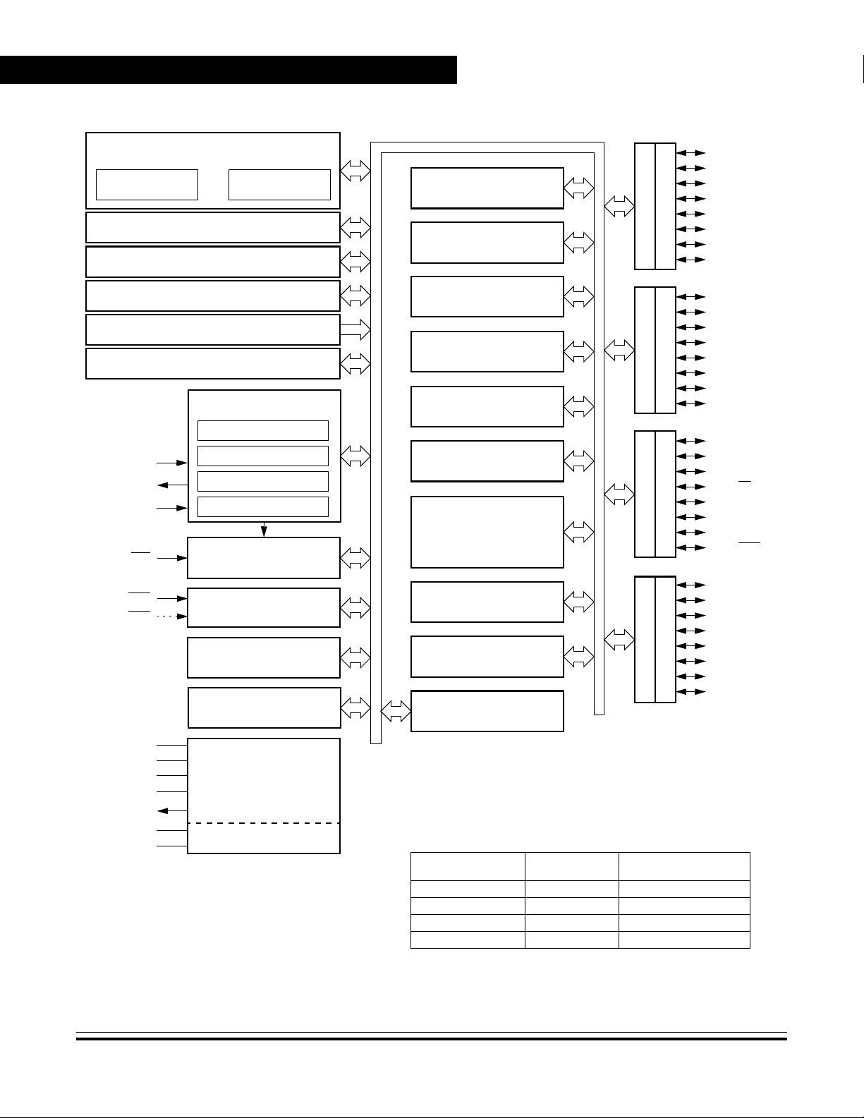
1.3 MCU Block Diagram
Figure 1-1 shows the structure of the MC68HC908AP64.
MC68HC908AP Family — Rev. 2.5 Data Sheet
MOTOROLA 25
For More Information On This Product,
Go to: www.freescale.com
General Description
M68HC08 CPU
CPU
REGISTERS
CONTROL AND STATUS REGISTERS — 96 BYTES
USER FLASH — (SEE TABLE)
ARITHMETIC/LOGIC
UNIT (ALU)
Freescale Semiconductor, Inc.
INTERNAL BUS
10-BIT ANALOG-TO-DIGITAL
CONVERTER MODULE
TIMEBASE
MODULE
DDRA
PTA7/ADC7
PTA6/ADC6
PTA5/ADC5
PTA4/ADC4
PORTA
PTA3/ADC3
PTA2/ADC2
PTA1/ADC1
PTA0/ADC0
‡
‡
‡
‡
‡
‡
‡
‡
nc...
I
cale Semiconductor,
Frees
USER RAM — (SEE TABLE)
MONITOR ROM — 959 BYTES
USER FLASH VECTOR SPACE — 48 BYTES
OSCILLATORS AND
CLOCK GENERATOR MODULE
INTERNAL OSCILLATOR
OSC1
OSC2
CGMXFC
* RST
* IRQ1
** IRQ2
VDD
VDDA
VSS
VSSA
VREG
VREFH
VREFL
RC OSCILLATOR
X-TAL OSCILLATOR
PHASE-LOCKED LOOP
SYSTEM INTEGRATION
MODULE
EXTERNAL INTERRUPT
MODULE
COMPUTER OPERATING
PROPERLY MODULE
POWER-ON RESET
MODULE
POWER
ADC REFERENCE
2-CHANNEL TIMER INTERFACE
2-CHANNEL TIMER INTERFACE
MODULATOR/DEMODULATOR)
* Pin contains integrated pullup device.
** Pin contains configurable pullup device.
*** Pin contains integrated pullup device when configured as KBI.
†
Pin is open-drain when configured as output.
‡
LED direct sink pin.
#
Pin not bonded on 42-pin SDIP.
MC68HC908AP64 2,048 62,368
MC68HC908AP32 2,048 32,768
MC68HC908AP16 1,024 16,384
MC68HC908AP8 1,024 8,192
MODULE 1
MODULE 2
SERIAL COMMUNICATIONS
INTERFACE MODULE 1
MULTI-MASTER IIC (SMBUS)
INTERFACE MODULE
SERIAL COMMUNICATIONS
INTERFACE MODULE 2
(WITH INFRARED
SERIAL PERIPHERAL
INTERFACE MODULE
KEYBOARD INTERRUPT
MODULE
LOW-VOLTAGE INHIBIT
MODULE
DEVICE
.
USER RAM
(bytes)
DDRB
DDRC
DDRD
USER FLASH
PORTB
PORTC
PORTD
(bytes)
PTB7/T2CH1
PTB6/T2CH0
PTB5/T1CH1
PTB4/T1CH0
PTB3/RxD
PTB2/TxD
PTB1/SCL
PTB0/SDA
PTC7/SCRxD
PTC6/SCTxD
PTC5/SPSCK
PTC4/SS
PTC3/MOSI
PTC2/MISO
PTC1
PTC0/IRQ2 **
PTD7/KBI7 ***
PTD6/KBI6 ***
PTD5/KBI5 ***
PTD4/KBI4 ***
PTD3/KBI3 ***
PTD2/KBI2 ***
PTD1/KBI1 ***
PTD0/KBI0 ***
†
†
†
†
#
†
†
#
Figure 1-1. MC68HC908AP64 Block Diagram
Data Sheet MC68HC908AP Family — Rev. 2.5
26 MOTOROLA
For More Information On This Product,
Go to: www.freescale.com

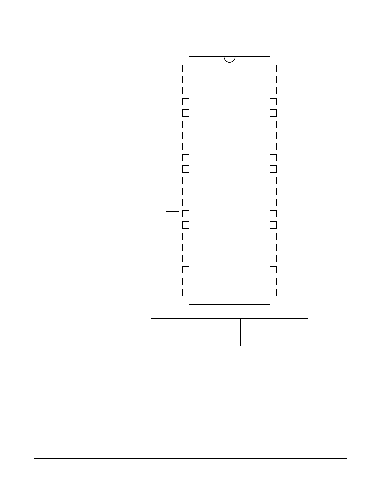
1.4 Pin Assignment
Freescale Semiconductor, Inc.
PTB6/T2CH0
1
PTB7/T2CH1
CGMXFC
48
47
PTD0/KBI0
46
PTD1/KBI1
45
PTD2/KBI2
44
VDDA
43
VSSA
42
PTD3/KBI3
41
PTD4/KBI4
40
PTD5/KBI5
39
General Description
Pin Assignment
PTD7/KBI7
PTD6/KBI6
37
38
36
VREFH
12
2
3
4
5
6
7
8
9
10
11
13
PTB1/SCL
14
15
PTB0/SDA
PTC6/SCTxD
PTC7/SCRxD
16
17
PTC5/SPSCK
18
19
PTC4/SS
PTC3/MOSI
20
21
22
PTC1
PTC2/MISO
PTC0/IRQ2
23
PTA7/ADC7
VREG
PTB5/T1CH1
nc...
I
PTB4/T1CH0
VDD
OSC1
OSC2
VSS
IRQ1
PTB3/RxD
RST
PTB2/TxD
cale Semiconductor,
35
34
33
32
31
30
29
28
27
26
24
NC
VREFL
NC
NC
PTA0/ADC0
NC
PTA1/ADC1
PTA2/ADC2
PTA3/ADC3
PTA4/ADC4
PTA5/ADC5
25
PTA6/ADC6
Frees
NC: No connection
Figure 1-2. 48-Pin LQFP Pin Assignments
MC68HC908AP Family — Rev. 2.5 Data Sheet
MOTOROLA 27
For More Information On This Product,
Go to: www.freescale.com
General Description
Freescale Semiconductor, Inc.
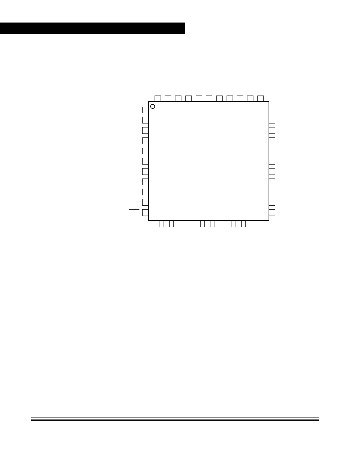
PTB6/T2CH0
PTB7/T2CH1
CGMXFC
44
43
42
41
1
40
39
VSSA
38
PTD3/KBI3
37
VDDA
PTD2/KBI2
PTD1/KBI1
PTD0/KBI0
PTD5/KBI5
PTD4/KBI4
36
35
PTD6/KBI6
34
33
PTD7/KBI7
VREG
PTB5/T1CH1
VDD
OSC1
nc...
I
OSC2
VSS
PTB4/T1CH0
IRQ1
PTB3/RxD
RST
cale Semiconductor,
11
2
3
4
5
6
7
8
9
10
12
PTB2/TxD
13
14
PTB1/SCL
PTB0/SDA
15
16
17
PTC6/SCTxD
PTC7/SCRxD
PTC5/SPSCK
18
19
PTC4/SS
PTC3/MOSI
20
PTC2/MISO
32
31
30
29
28
27
26
25
24
21
22
PTC1
PTC0/IRQ2
Figure 1-3. 44-Pin QFP Pin Assignments
VREFH
VREFL
PTA0/ADC0
PTA1/ADC1
PTA2/ADC2
PTA3/ADC3
PTA4/ADC4
PTA5/ADC5
PTA6/ADC6
PTA7/ADC7
23
Frees
Data Sheet MC68HC908AP Family — Rev. 2.5
28 MOTOROLA
For More Information On This Product,
Go to: www.freescale.com
Freescale Semiconductor, Inc.
General Description
Pin Assignment
nc...
I
cale Semiconductor,
Frees
PTD2/KBI2
PTD1/KBI1
PTD0/KBI0
PTB7/T2CH1
CGMXFC
PTB6/T2CH0
VREG
PTB5/T1CH1
VDD
OSC1
OSC2
VSS
PTB4/T1CH0
IRQ1
PTB3/RxD
RST
PTB2/TxD
PTB1/SCL
PTB0/SDA
PTC7/SCRxD
PTC6/SCTxD
Pins not available on 42-pin package Internal connection
1
2
3
4
5
6
7
8
9
10
11
12
13
14
15
16
17
18
19
20
21 22
PTC0/IRQ2
PTC1 Unconnected
42
41
40
39
38
37
36
35
34
33
32
31
30
29
28
27
26
25
24
23
Unconnected
VDDA
VSSA
PTD3/KBI3
PTD4/KBI4
PTD5/KBI5
PTD6/KBI6
PTD7/KBI7
VREFH
VREFL
PTA0/ADC0
PTA1/ADC1
PTA2/ADC2
PTA3/ADC3
PTA4/ADC4
PTA5/ADC5
PTA6/ADC6
PTA7/ADC7
PTC2/MISO
PTC3/MOSI
PTC4/SS
PTC5/SPSCK
Figure 1-4. 42-Pin SDIP Pin Assignment
MC68HC908AP Family — Rev. 2.5 Data Sheet
MOTOROLA 29
For More Information On This Product,
Go to: www.freescale.com
General Description
1.5 Pin Functions
Description of the pin functions are provided in Table 1-2.
Freescale Semiconductor, Inc.
Table 1-2. Pin Functions
nc...
I
cale Semiconductor,
Frees
PIN NAME PIN DESCRIPTION IN/OUT
V
V
V
V
V
V
V
DD
SS
DDA
SSA
REFH
REFL
REG
Power supply. In
Power supply ground. Out 0 V
Power supply for analog circuits. In
Power supply ground for analog circuits. Out
ADC input reference high. In
ADC input reference low. Out
Internal (2.5 V) regulator output.
Require external capacitors for decoupling.
Out
RST
IRQ1
OSC1 Crystal or RC oscillator input. In
OSC2
Reset input, active low; with internal pullup and schmitt
trigger input.
External IRQ1 pin; with internal pullup and schmitt trigger
input.
Used for mode entry selection. In
Crystal OSC option: crystal oscillator output; inverted
OSC1.
RC OSC option: bus clock output. Out
Internal OSC option: bus clock output. Out
In
In
Out
VOLTAGE
LEVEL
4.5 to 5.5
or
2.7 to 3.3
V
DD
V
SS
V
DDA
V
SSA
(1)
2.5V
V
DD
V
DD
V
to V
DD
V
V
V
V
TST
REG
REG
REG
REG
CGMXFC CGM external filter capacitor connection. In/Out Analog
PTA0/ADC0
:
PTA7/ADC7
Data Sheet MC68HC908AP Family — Rev. 2.5
30 MOTOROLA
8-bit general purpose I/O port. In/Out
Pins as ADC inputs, ADC0–ADC7. In
Each pin has high current sink for LED. Out
For More Information On This Product,
Go to: www.freescale.com
V
V
V
DD
REFH
DD
Freescale Semiconductor, Inc.
Table 1-2. Pin Functions
General Description
Pin Functions
PIN NAME PIN DESCRIPTION IN/OUT
8-bit general purpose I/O port; PTB0–PTB3 are open drain
when configured as output. PTB4–PTB7 have schmitt
trigger inputs.
PTB0/SDA
PTB1/SCL
PTB2/TxD
PTB3/RxD
PTB4/T1CH0
nc...
I
cale Semiconductor,
PTB5/T1CH1
PTB6/T2CH0
PTB7/T2CH1
PTC0/IRQ2
PTC1
PTC2/MISO
PTC3/MOSI
PTC4/SS
PTC5/SPSCK
PTC6/SCTxD
PTC7/SCRxD
PTB0 as SDA of MMIIC. In/Out
PTB1 as SCL of MMIIC. In/Out
PTB2 as TxD of SCI; open drain output. Out
PTB3 as RxD of SCI. In
PTB4 as T1CH0 of TIM1. In/Out
PTB5 as T1CH1 of TIM1. In/Out
PTB6 as T2CH0 of TIM2. In/Out
PTB7 as T2CH1 of TIM2. In/Out
8-bit general purpose I/O port; PTC6 and PTC7 are open
drain when configured as output.
PTC0 is shared with IRQ2 and has schmitt trigger input. In
PTC2 as MISO of SPI. In
PTC3 as MOSI of SPI. Out
PTC4 as SS of SPI. In
PTC5 as SPSCK of SPI. In/Out
PTC6 as SCTxD of IRSCI; open drain output. Out
PTC7 as SCRxD of IRSCI. In
In/Out
In/Out
VOLTAGE
LEVEL
V
DD
V
DD
V
DD
V
DD
V
DD
V
DD
V
DD
V
DD
V
DD
V
DD
V
DD
V
DD
V
DD
V
DD
V
DD
V
DD
V
DD
Frees
PTD0/KBI0
:
PTD7/KBI7
Notes:
1. See Section 24. Electrical Specifications for V
MC68HC908AP Family — Rev. 2.5 Data Sheet
MOTOROLA 31
8-bit general purpose I/O port with schmitt trigger inputs. In/Out
Pins as keyboard interrupts (with pullup), KBI0–KBI7. In
tolerance.
REG
For More Information On This Product,
Go to: www.freescale.com
V
V
DD
DD

Freescale Semiconductor, Inc.
General Description
1.6 Power Supply Bypassing (VDD, VDDA, VSS, VSSA)
VDD and VSS are the power supply and ground pins, the MCU operates
from a single power supply together with an on chip voltage regulator.
Fast signal transitions on MCU pins place high. short-duration current
demands on the power supply. To prevent noise problems, take special
care to provide power supply bypassing at the MCU as Figure 1-5
shows. Place the bypass capacitors as close to the MCU power pins as
possible. Use high-frequency-response ceramic capacitor for C
C
that require the port pins to source high current level.
are optional bulk current bypass capacitors for use in applications
BULK
BYPASS
,
nc...
I
cale Semiconductor,
Frees
V
DDA
and V
are the power supply and ground pins for the analog
SSA
circuits of the MCU. These pins should be decoupled as per the digital
power supply pins.
MCU
V
DD
C1(a)
0.1 µF
+
C2(a)
V
DD
NOTE: Component values shown represent typical applications.
V
SS
V
DDA
C1(b)
0.1 µF
+
C2(b)
V
DD
V
SSA
Figure 1-5. Power Supply Bypassing
Data Sheet MC68HC908AP Family — Rev. 2.5
32 MOTOROLA
For More Information On This Product,
Go to: www.freescale.com

Freescale Semiconductor, Inc.
Regulator Power Supply Configuration (VREG)
1.7 Regulator Power Supply Configuration (VREG)
V
is the output from the on-chip regulator. All internal logics, except
REG
for the I/O pads, are powered by V
ceramic bypass capacitor of 100 nF as Figure 1-6 shows. Place the
bypass capacitor as close to the V
output. V
REG
REG
MCU
requires an external
REG
pin as possible.
General Description
V
REG
nc...
I
C
VREGBYPASS
100 nF
Figure 1-6. Regulator Power Supply Bypassing
cale Semiconductor,
V
SS
Frees
MC68HC908AP Family — Rev. 2.5 Data Sheet
MOTOROLA 33
For More Information On This Product,
Go to: www.freescale.com

Freescale Semiconductor, Inc.
General Description
nc...
I
cale Semiconductor,
Frees
Data Sheet MC68HC908AP Family — Rev. 2.5
34 MOTOROLA
For More Information On This Product,
Go to: www.freescale.com

Freescale Semiconductor, Inc.
Data Sheet – MC68HC908AP Family
2.1 Introduction
The CPU08 can address 64k-bytes of memory space. The memory map,
shown in Figure 2-1, includes:
Section 2. Memory Map
nc...
I
cale Semiconductor,
Frees
• 62,368 bytes of user FLASH — MC68HC908AP64
32,768 bytes of user FLASH — MC68HC908AP32
16,384 bytes of user FLASH — MC68HC908AP16
8,192 bytes of user FLASH — MC68HC908AP8
• 2,048 bytes of RAM — MC68HC908AP64 and MC68HC908AP32
1,024 bytes of RAM — MC68HC908AP16 and MC68HC908AP8
• 48 bytes of user-defined vectors
• 959 bytes of monitor ROM
2.2 Unimplemented Memory Locations
Accessing an unimplemented location can cause an illegal address
reset if illegal address resets are enabled. In the memory map
(Figure 2-1) and in register figures in this document, unimplemented
locations are shaded.
2.3 Reserved Memory Locations
Accessing a reserved location can have unpredictable effects on MCU
operation. In the Figure 2-1 and in register figures in this document,
reserved locations are marked with the word Reserved or with the
letter R.
MC68HC908AP Family — Rev. 2.5 Data Sheet
MOTOROLA 35
For More Information On This Product,
Go to: www.freescale.com

Freescale Semiconductor, Inc.
Memory Map
2.4 Input/Output (I/O) Section
Most of the control, status, and data registers are in the zero page area
of $0000–$005F. Additional I/O registers have these addresses:
• $FE00; SIM break status register, SBSR
• $FE01; SIM reset status register, SRSR
• $FE02; Reserved
• $FE03; SIM break flag control register, SBFCR
• $FE04; interrupt status register 1, INT1
nc...
I
cale Semiconductor,
Frees
• $FE05; interrupt status register 2, INT2
• $FE06; interrupt status register 3, INT3
• $FE07; Reserved
• $FE08; FLASH control register, FLCR
• $FE09; FLASH block protect register, FLBPR
• $FE0A; Reserved
• $FE0B; Reserved
• $FE0C; Break address register high, BRKH
• $FE0D; Break address register low, BRKL
• $FE0E; Break status and control register, BRKSCR
• $FE0F; LVI Status register, LVISR
• $FFCF; Mask option register, MOR (FLASH register)
• $FFFF; COP control register, COPCTL
Data registers are shown in Figure 2-2. Table 2-1 is a list of vector
locations.
Data Sheet MC68HC908AP Family — Rev. 2.5
36 MOTOROLA
For More Information On This Product,
Go to: www.freescale.com

Freescale Semiconductor, Inc.
Memory Map
Input/Output (I/O) Section
nc...
I
cale Semiconductor,
Frees
$0000
↓
$005F
$0060
↓
$085F
$0860
↓
$FBFF
$FC00
↓
$FDFF
$FE00 SIM Break Status Register
$FE01 SIM Reset Status Register
$FE02 Reserved
$FE03 SIM Break Flag Control Register
$FE04 Interrupt Status Register 1
$FE05 Interrupt Status Register 2
$FE06 Interrupt Status Register 3
$FE07 Reserved
$FE08 FLASH Control Register
$FE09 FLASH Block Protect Register
$FE0A Reserved
$FE0B Reserved
$FE0C Break Address Register High
$FE0D Break Address Register Low
$FE0E Break Status and Control Register
$FE0F LVI Status Register
$FE10
↓
$FFCE
$FFCF Mask Option Register
$FFD0
↓
$FFFF
I/O Registers
96 Bytes
RAM
2,048 Bytes
(MC68HC908AP64)
FLASH Memory
62,368 Bytes
(MC68HC908AP64)
Monitor ROM 2
512 Bytes
Monitor ROM 1
447 Bytes
FLASH Vectors
48 Bytes
MC68HC908AP32 MC68HC908AP16 MC68HC908AP8
RAM
2,048 Bytes
FLASH Memory
32,768 Bytes
Unimplemented
29,600 Bytes
$0060
↓
$085F
$0860
↓
$885F
$8860
↓
$FBFF
RAM
1,024 Bytes
Unimplemented
1,024 Bytes
FLASH Memory
16,384 Bytes
Unimplemented
45,984 Bytes
$0060
$045F
$0860
↓
$485F
$4860
↓
$FBFF
RAM
1,024 Bytes
Unimplemented
1,024 Bytes
FLASH Memory
8,192 Bytes
Unimplemented
54,176 Bytes
Figure 2-1. Memory Map
$0060
$045F
$0860
$285F
$2860
↓
$FBFF
MC68HC908AP Family — Rev. 2.5 Data Sheet
MOTOROLA 37
For More Information On This Product,
Go to: www.freescale.com

Freescale Semiconductor, Inc.
Memory Map
Addr.Register Name Bit 7654321Bit 0
nc...
I
cale Semiconductor,
Frees
Read:
$0000
$0001
$0002
$0003
$0004
$0005
$0006
$0007
$0008
Port A Data Register
(PTA)
Port B Data Register
(PTB)
Port C Data Register
(PTC)
Port D Data Register
(PTD)
Data Direction Register A
(DDRA)
Data Direction Register B
(DDRB)
Data Direction Register C
(DDRC)
Data Direction Register D
(DDRD)
Unimplemented
Write:
Reset: Unaffected by reset
Read:
Write:
Reset: Unaffected by reset
Read:
Write:
Reset: Unaffected by reset
Read:
Write:
Reset: Unaffected by reset
Read:
Write:
Reset:00000000
Read:
Write:
Reset:00000000
Read:
Write:
Reset:00000000
Read:
Write:
Reset:00000000
Read:
Write:
PTA7 PTA6 PTA5 PTA4 PTA3 PTA2 PTA1 PTA0
PTB7 PTB6 PTB5 PTB4 PTB3 PTB2 PTB1 PTB0
PTC7 PTC6 PTC5 PTC4 PTC3 PTC2 PTC1 PTC0
PTD7 PTD6 PTD5 PTD4 PTD3 PTD2 PTD1 PTD0
DDRA7 DDRA6 DDRA5 DDRA4 DDRA3 DDRA2 DDRA1 DDRA0
DDRB7 DDRB6 DDRB5 DDRB4 DDRB3 DDRB2 DDRB1 DDRB0
DDRC7 DDRC6 DDRC5 DDRC4 DDRC3 DDRC2 DDRC1 DDRC0
DDRD7 DDRD6 DDRD5 DDRD4 DDRD3 DDRD2 DDRD1 DDRD0
Reset:
Read:
$0009 Unimplemented
U = Unaffected X = Indeterminate
Write:
Reset:
= Unimplemented R = Reserved
Figure 2-2. Control, Status, and Data Registers (Sheet 1 of 12)
Data Sheet MC68HC908AP Family — Rev. 2.5
38 MOTOROLA
For More Information On This Product,
Go to: www.freescale.com

Freescale Semiconductor, Inc.
Addr.Register Name Bit 7654321Bit 0
Read:
Memory Map
Input/Output (I/O) Section
nc...
I
cale Semiconductor,
Frees
$000A Unimplemented
$000B Unimplemented
Port-A LED Control
$000C
$000D Unimplemented
$000E Unimplemented
$000F Unimplemented
$0010
$0011
$0012
SPI Control Register
SPI Status and Control
SPI Data Register
Register
(LEDA)
(SPCR)
Register
(SPSCR)
(SPDR)
Write:
Reset:
Read:
Write:
Reset:
Read:
Write:
Reset:00000000
Read:
Write:
Reset:
Read:
Write:
Reset:
Read:
Write:
Reset:
Read:
Write:
Reset:00101000
Read: SPRF
Write:
Reset:00001000
Read: R7 R6 R5 R4 R3 R2 R1 R0
Write: T7 T6 T5 T4 T3 T2 T1 T0
Reset: Unaffected by reset
LEDA7 LEDA6 LEDA5 LEDA4 LEDA3 LEDA2 LEDA1 LEDA0
SPRIE R SPMSTR CPOL CPHA SPWOM SPE SPTIE
ERRIE
OVRF MODF SPTE
MODFEN SPR1 SPR0
$0013
Read:
SCI Control Register 1
(SCC1)
U = Unaffected X = Indeterminate
Write:
Reset:00000000
LOOPS ENSCI TXINV M WAKE ILTY PEN PTY
= Unimplemented R = Reserved
Figure 2-2. Control, Status, and Data Registers (Sheet 2 of 12)
MC68HC908AP Family — Rev. 2.5 Data Sheet
MOTOROLA 39
For More Information On This Product,
Go to: www.freescale.com

Freescale Semiconductor, Inc.
Memory Map
Addr.Register Name Bit 7654321Bit 0
nc...
I
cale Semiconductor,
Frees
Read:
$0014
$0015
$0016
$0017
$0018
$0019
$001A
$001B
$001C
SCI Control Register 2
(SCC2)
SCI Control Register 3
(SCC3)
SCI Status Register 1
(SCS1)
SCI Status Register 2
(SCS2)
SCI Data Register
(SCDR)
SCI Baud Rate Register
(SCBR)
Keyboard Status and
Control Register
(KBSCR)
Keyboard Interrupt
Enable Register
(KBIER)
IRQ2 Status and Control
Register
(INTSCR2)
Write:
Reset:00000000
Read: R8
Write:
Reset:UU000000
Read: SCTE TC SCRF IDLE OR NF FE PE
Write:
Reset:11000000
Read: 000000BKFRPF
Write:
Reset:00000000
Read: R7 R6 R5 R4 R3 R2 R1 R0
Write: T7 T6 T5 T4 T3 T2 T1 T0
Reset: Unaffected by reset
Read: 0 0
Write:
Reset:00000000
Read: 0000KEYF 0
Write:
Reset:00000000
Read:
Write:
Reset:00000000
Read: 0
Write:
Reset:00000000
SCTIE TCIE SCRIE ILIE TE RE RWU SBK
T8 DMARE DMATE ORIE NEIE FEIE PEIE
SCP1 SCP0 R SCR2 SCR1 SCR0
ACK
KBIE7 KBIE6 KBIE5 KBIE4 KBIE3 KBIE2 KBIE1 KBIE0
00IRQ2F0
PUC0ENB
ACK2
IMASK MODE
IMASK2 MODE2
Read:
$001D
† One-time writable register after each reset.
Configuration Register 2
(CONFIG2)
U = Unaffected X = Indeterminate
Write:
†
Reset:00000000
STOP_
ICLKDIS
STOP_
RCLKEN
STOP_
XCLKEN
OSCCLK1 OSCCLK0
= Unimplemented R = Reserved
00
SCIBD-
SRC
Figure 2-2. Control, Status, and Data Registers (Sheet 3 of 12)
Data Sheet MC68HC908AP Family — Rev. 2.5
40 MOTOROLA
For More Information On This Product,
Go to: www.freescale.com

Freescale Semiconductor, Inc.
Addr.Register Name Bit 7654321Bit 0
Memory Map
Input/Output (I/O) Section
IRQ1 Status and Control
$001E
(INTSCR1)
$001F
† One-time writable register after each reset.
$0020
nc...
I
$0021
$0022
$0023
$0024
Configuration Register 1
(CONFIG1)
Timer 1 Status and
Control Register
Timer 1 Counter
Register High
(T1CNTH)
Timer 1 Counter
Register Low
(T1CNTL)
Timer 1 Counter Modulo
Register High
(T1MODH)
Timer 1 Counter Modulo
Register Low
(T1MODL)
cale Semiconductor,
Timer 1 Channel 0 Status
$0025
Frees
$0026
and Control Register
Timer 1 Channel 0
Register High
(T1CH0H)
Register
(T1SC)
(T1SC0)
Read: 0000IRQ1F0
Write:
Reset:00000000
Read:
Write:
†
Reset:00000000
Read: TOF
Write: 0 TRST
Reset:00100000
Read: Bit 15 14 13 12 11 10 9 Bit 8
Write:
Reset:00000000
Read: Bit 7 654321Bit 0
Write:
Reset:00000000
Read:
Write:
Reset:11111111
Read:
Write:
Reset:11111111
Read: CH0F
Write: 0
Reset:00000000
Read:
Write:
Reset: Indeterminate after reset
COPRS LVISTOP LVIRSTD LVIPWRD LVIREGD SSREC STOP COPD
00
TOIE TSTOP
Bit 15 14 13 12 11 10 9 Bit 8
Bit 7654321Bit 0
CH0IE MS0B MS0A ELS0B ELS0A TOV0 CH0MAX
Bit 15 14 13 12 11 10 9 Bit 8
ACK1
PS2 PS1 PS0
IMASK1 MODE1
Read:
Bit 7654321Bit 0
Write:
Reset: Indeterminate after reset
= Unimplemented R = Reserved
$0027
Timer 1 Channel 0
Register Low
(T1CH0L)
U = Unaffected X = Indeterminate
Figure 2-2. Control, Status, and Data Registers (Sheet 4 of 12)
MC68HC908AP Family — Rev. 2.5 Data Sheet
MOTOROLA 41
For More Information On This Product,
Go to: www.freescale.com
Freescale Semiconductor, Inc.
Memory Map
Addr.Register Name Bit 7654321Bit 0
nc...
I
cale Semiconductor,
Frees
Timer 1 Channel 1 Status
$0028
$0029
$002A
$002B
$002C
$002D
$002E
$002F
$0030
and Control Register
(T1SC1)
Timer 1 Channel 1
Register High
(T1CH1H)
Timer 1 Channel 1
Register Low
(T1CH1L)
Timer 2 Status and
Control Register
(T2SC)
Timer 2 Counter
Register High
(T2CNTH)
Timer 2 Counter
Register Low
(T2CNTL)
Timer 2 Counter Modulo
Register High
(T2MODH)
Timer 2 Counter Modulo
Register Low
(T2MODL)
Timer 2 Channel 0 Status
and Control Register
(T2SC0)
Read: CH1F
CH1IE
Write: 0
Reset:00000000
Read:
Bit 15 14 13 12 11 10 9 Bit 8
Write:
Reset: Indeterminate after reset
Read:
Bit 7654321Bit 0
Write:
Reset: Indeterminate after reset
Read: TOF
TOIE TSTOP
Write: 0 TRST
Reset:00100000
Read: Bit 15 14 13 12 11 10 9 Bit 8
Write:
Reset:00000000
Read: Bit 7 654321Bit 0
Write:
Reset:00000000
Read:
Bit 15 14 13 12 11 10 9 Bit 8
Write:
Reset:11111111
Read:
Bit 7654321Bit 0
Write:
Reset:11111111
Read: CH0F
CH0IE MS0B MS0A ELS0B ELS0A TOV0 CH0MAX
Write: 0
Reset:00000000
0
MS1A ELS1B ELS1A TOV1 CH1MAX
00
PS2 PS1 PS0
Read:
Bit 15 14 13 12 11 10 9 Bit 8
Write:
Reset: Indeterminate after reset
= Unimplemented R = Reserved
$0031
Timer 2 Channel 0
Register High
(T2CH0H)
U = Unaffected X = Indeterminate
Figure 2-2. Control, Status, and Data Registers (Sheet 5 of 12)
Data Sheet MC68HC908AP Family — Rev. 2.5
42 MOTOROLA
For More Information On This Product,
Go to: www.freescale.com
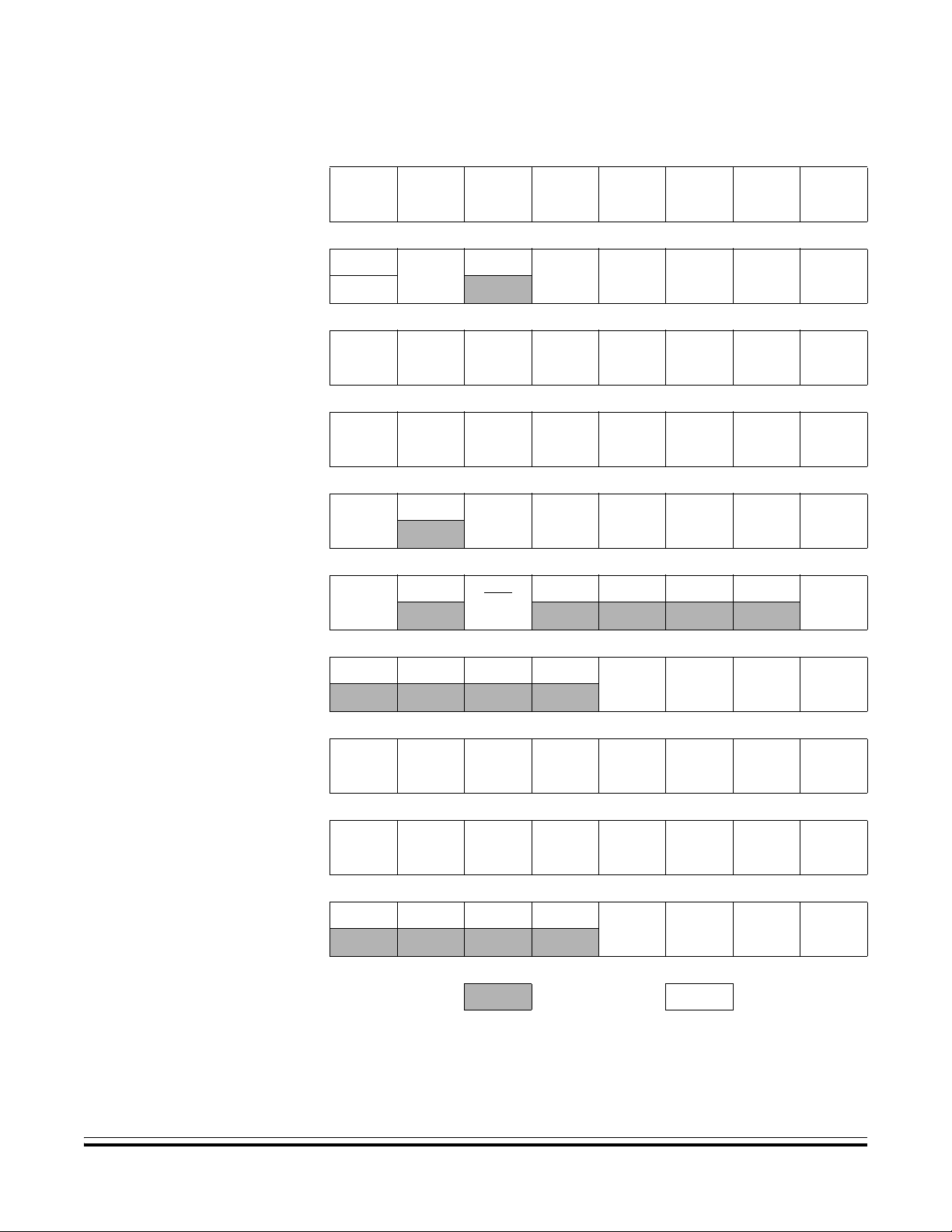
Freescale Semiconductor, Inc.
Addr.Register Name Bit 7654321Bit 0
Memory Map
Input/Output (I/O) Section
nc...
I
cale Semiconductor,
Frees
$0032
$0033
$0034
$0035
$0036
$0037
$0038
$0039
$003A
Timer 2 Channel 0
Register Low
(T2CH0L)
Timer 2 Channel 1 Status
and Control Register
(T2SC1)
Timer 2 Channel 1
Register High
(T2CH1H)
Timer 2 Channel 1
Register Low
(T2CH1L)
PLL Control Register
(PCTL)
PLL Bandwidth Control
Register
(PBWC)
PLL Multiplier Select
Register High
(PMSH)
PLL Multiplier Select
Register Low
(PMSL)
PLL VCO Range Select
Register
(PMRS)
Read:
Write:
Reset: Indeterminate after reset
Read: CH1F
Write: 0
Reset:00000000
Read:
Write:
Reset: Indeterminate after reset
Read:
Write:
Reset: Indeterminate after reset
Read:
Write:
Reset:00100000
Read:
Write:
Reset:00000000
Read: 0000
Write:
Reset:00000000
Read:
Write:
Reset:01000000
Read:
Write:
Reset:01000000
Bit 7654321Bit 0
CH1IE
Bit 15 14 13 12 11 10 9 Bit 8
Bit 7654321Bit 0
PLLF
PLLIE
LOCK
AUTO
MUL7 MUL6 MUL5 MUL4 MUL3 MUL2 MUL1 MUL0
VRS7 VRS6 VRS5 VRS4 VRS3 VRS2 VRS1 VRS0
0
PLLON BCS PRE1 PRE0 VPR1 VPR0
ACQ
MS1A ELS1B ELS1A TOV1 CH1MAX
0000
R
MUL11 MUL10 MUL9 MUL8
Read: 0000
RDS3 RDS2 RDS1 RDS0
Write:
Reset:00000001
= Unimplemented R = Reserved
$003B
PLL Reference Divider
Select Register
(PMDS)
U = Unaffected X = Indeterminate
Figure 2-2. Control, Status, and Data Registers (Sheet 6 of 12)
MC68HC908AP Family — Rev. 2.5 Data Sheet
MOTOROLA 43
For More Information On This Product,
Go to: www.freescale.com

Freescale Semiconductor, Inc.
Memory Map
Addr.Register Name Bit 7654321Bit 0
Read:
nc...
I
cale Semiconductor,
Frees
$003C Unimplemented
$003D Unimplemented
$003E Unimplemented
$003F Unimplemented
$0040
$0041
$0042
$0043
$0044
IRSCI Control Register 1
IRSCI Control Register 2
IRSCI Control Register 3
IRSCI Status Register 1
IRSCI Status Register 2
(IRSCC1)
(IRSCC2)
(IRSCC3)
(IRSCS1)
(IRSCS2)
Write:
Reset:
Read:
Write:
Reset:
Read:
Write:
Reset:
Read:
Write:
Reset:
Read:
LOOPS ENSCI
Write:
Reset:00000000
Read:
SCTIE TCIE SCRIE ILIE TE RE RWU SBK
Write:
Reset:00000000
Read: R8
T8 DMARE DMATE ORIE NEIE FEIE PEIE
Write:
Reset:UU000000
Read: SCTE TC SCRF IDLE OR NF FE PE
Write:
Reset:11000000
Read:
Write:
Reset:00000000
0
M WAKE ILTY PEN PTY
BKF RPF
Read: R7 R6 R5 R4 R3 R2 R1 R0
$0045
IRSCI Data Register
(IRSCDR)
U = Unaffected X = Indeterminate
Write: T7 T6 T5 T4 T3 T2 T1 T0
Reset: Unaffected by reset
= Unimplemented R = Reserved
Figure 2-2. Control, Status, and Data Registers (Sheet 7 of 12)
Data Sheet MC68HC908AP Family — Rev. 2.5
44 MOTOROLA
For More Information On This Product,
Go to: www.freescale.com

Freescale Semiconductor, Inc.
Addr.Register Name Bit 7654321Bit 0
Memory Map
Input/Output (I/O) Section
nc...
I
cale Semiconductor,
Frees
$0046
$0047
$0048
$0049
$004A
$004B
$004C
$004D
$004E
IRSCI Baud Rate Register
IRSCI Infrared Control
MMIIC Address Register
MMIIC Control Register 1
MMIIC Control Register 2
MMIIC Status Register
MMIIC Data Transmit
MMIIC Data Receive
MMIIC CRC Data Register
(IRSCBR)
Register
(IRSCIRCR)
(MMADR)
(MMCR1)
(MMCR2)
(MMSR)
Register
(MMDTR)
Register
(MMDRR)
(MMCRDR)
Read:
Write:
Reset:00000000
Read:
Write:
Reset:00000000
Read:
Write:
Reset:10100000
Read:
Write:
Reset:00000000
Read: MMALIF MMNAKIF MMBB
Write: 0 0
Reset:00 0 0000Unaffected
Read: MMRXIF MMTXIF MMATCH MMSRW MMRXAK
Write: 0 0
Reset:00 0 01010
Read:
Write:
Reset:00000000
Read: MMRD7 MMRD6 MMRD5 MMRD4 MMRD3 MMRD2 MMRD1 MMRD0
Write:
Reset:00000000
Read:
Write:
CKS
R
MMAD7 MMAD6 MMAD5 MMAD4 MMAD3 MMAD2 MMAD1 MMEXTAD
MMEN MMIEN
MMTD7 MMTD6 MMTD5 MMTD4 MMTD3 MMTD2 MMTD1 MMTD0
MMCRCD7 MMCRCD6 MMCRCD5 MMCRCD4 MMCRCD3 MMCRCD2 MMCRCD1 MMCRCD0
0
SCP1 SCP0 R SCR2 SCR1 SCR0
0 0 0
0 0
MMTXAK REPSEN
MMCLRBB
MMAST MMRW
R TNP1 TNP0 IREN
MMCRCBYTE
0 0
MMCRCBF
MMTXBE MMRXBF
0
MMCRCEF
Reset:00000000
Read: 0 0 0 0 0
MMBR2 MMBR1 MMBR0
Write:
Reset:00000100
= Unimplemented R = Reserved
$004F
MMIIC Frequency Divider
Register
(MMFDR)
U = Unaffected X = Indeterminate
Figure 2-2. Control, Status, and Data Registers (Sheet 8 of 12)
MC68HC908AP Family — Rev. 2.5 Data Sheet
MOTOROLA 45
For More Information On This Product,
Go to: www.freescale.com
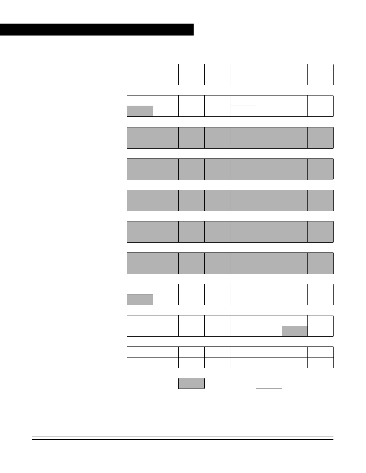
Freescale Semiconductor, Inc.
Memory Map
Addr.Register Name Bit 7654321Bit 0
nc...
I
cale Semiconductor,
Frees
$0050 Reserved
Timebase Control
$0051
$0052 Unimplemented
$0053 Unimplemented
$0054 Unimplemented
$0055 Unimplemented
$0056 Unimplemented
ADC Status and Control
$0057
ADC Clock Control
$0058
Register
(TBCR)
Register
(ADSCR)
Register
(ADICLK)
Read:
Write:
Reset:
Read: TBIF
Write:
Reset:00000000
Read:
Write:
Reset:
Read:
Write:
Reset:
Read:
Write:
Reset:
Read:
Write:
Reset:
Read:
Write:
Reset:
Read: COCO
Write:
Reset:00011111
Read:
Write:
Reset:00000000
RRRRRRRR
TBR2 TBR1 TBR0
AIEN ADCO ADCH4 ADCH3 ADCH2 ADCH1 ADCH0
ADIV2 ADIV1 ADIV0 ADICLK MODE1 MODE0
0
TBIE TBON R
TACK
0 0
R
Read: ADx ADx ADx ADx ADx ADx ADx ADx
$0059
ADC Data Register High 0
(ADRH0)
U = Unaffected X = Indeterminate
Write:RRRRRRRR
Reset:00000000
= Unimplemented R = Reserved
Figure 2-2. Control, Status, and Data Registers (Sheet 9 of 12)
Data Sheet MC68HC908AP Family — Rev. 2.5
46 MOTOROLA
For More Information On This Product,
Go to: www.freescale.com
Freescale Semiconductor, Inc.
Addr.Register Name Bit 7654321Bit 0
Memory Map
Input/Output (I/O) Section
$005A
$005B
$005C ADC Data Register Low 2
nc...
I
cale Semiconductor,
$005D
$005E
$005F Unimplemented
$FE00
Note: Writing a logic 0 clears SBSW.
$FE01
ADC Data Register Low 0
ADC Data Register Low 1
ADC Data Register Low 3
ADC Auto-scan Control
SIM Break Status Register
SIM Reset Status Register
Frees
(ADRL0)
(ADRL1)
(ADRL2)
(ADRL3)
Register
(ADASCR)
(SBSR)
(SRSR)
Read: ADx ADx ADx ADx ADx ADx ADx ADx
Write:RRRRRRRR
Reset:00000000
Read: AD9 AD8 AD7 AD6 AD5 AD4 AD3 AD2
Write:RRRRRRRR
Reset:00000000
Read: AD9 AD8 AD7 AD6 AD5 AD4 AD3 AD2
Write:RRRRRRRR
Reset:00000000
Read: AD9 AD8 AD7 AD6 AD5 AD4 AD3 AD2
Write:RRRRRRRR
Reset:00000000
Read:
Write:
Reset:00000000
Read:
Write:
Reset:
Read:
RRRRRR
Write: Note
Reset: 0
Read: POR PIN COP ILOP ILAD MODRST LVI 0
Write:
Reset:10000000
AUTO1 AUTO0 ASCAN
SBSW
R
$FE02 Reserved
U = Unaffected X = Indeterminate
Read:
Write:
Reset:
RRRRRRRR
= Unimplemented R = Reserved
Figure 2-2. Control, Status, and Data Registers (Sheet 10 of 12)
MC68HC908AP Family — Rev. 2.5 Data Sheet
MOTOROLA 47
For More Information On This Product,
Go to: www.freescale.com

Freescale Semiconductor, Inc.
Memory Map
Addr.Register Name Bit 7654321Bit 0
nc...
I
cale Semiconductor,
Frees
SIM Break Flag Control
$FE03
$FE04
$FE05
$FE06
$FE07 Reserved
$FE08
$FE09
$FE0A Reserved
$FE0B Reserved
Interrupt Status Register 1
Interrupt Status Register 2
Interrupt Status Register 3
FLASH Control Register
FLASH Block Protect
Register
(SBFCR)
(INT1)
(INT2)
(INT3)
(FLCR)
Register
(FLBPR)
Read:
BCFERRRRRRR
Write:
Reset: 0
Read: IF6 IF5 IF4 IF3 IF2 IF1 0 0
Write:RRRRRRRR
Reset:00000000
Read: IF14 IF13 IF12 IF11 IF10 IF9 IF8 IF7
Write:RRRRRRRR
Reset:00000000
Read: 0 IF21 IF20 IF19 IF18 IF17 IF16 IF15
Write:RRRRRRRR
Reset:00000000
Read:
RRRRRRRR
Write:
Reset:
Read: 0000
HVEN MASS ERASE PGM
Write:
Reset:00000000
Read:
BPR7 BPR6 BPR5 BPR4 BPR3 BPR2 BPR1 BPR0
Write:
Reset:00000000
Read:
RRRRRRRR
Write:
Reset:
Read:
RRRRRRRR
Write:
Reset:
Read:
Bit 15 14 13 12 11 10 9 Bit 8
Write:
Reset:00000000
= Unimplemented R = Reserved
$FE0C
Break Address
Register High
(BRKH)
U = Unaffected X = Indeterminate
Figure 2-2. Control, Status, and Data Registers (Sheet 11 of 12)
Data Sheet MC68HC908AP Family — Rev. 2.5
48 MOTOROLA
For More Information On This Product,
Go to: www.freescale.com

Freescale Semiconductor, Inc.
Addr.Register Name Bit 7654321Bit 0
Memory Map
Input/Output (I/O) Section
Break Address
$FE0D
Break Status and Control
$FE0E
$FE0F
nc...
I
$FFCF
$FFFF
#
MOR is a non-volatile FLASH register; write by programming.
Mask Option Register
COP Control Register
Register Low
(BRKL)
Register
(BRKSCR)
LVI Status Register
(LVISR)
(MOR)
(COPCTL)
U = Unaffected X = Indeterminate
Figure 2-2. Control, Status, and Data Registers (Sheet 12 of 12)
cale Semiconductor,
Read:
Write:
Reset:00000000
Reset:
Read:
Write:00000000
Reset:LVIOUT 0000000
Read:
Write:00000000
Read:
Write:
#
Erased:
Reset:UUUUUUUU
Read: Low byte of reset vector
Write: Writing clears COP counter (any value)
Reset: Unaffected by reset
Bit 7654321Bit 0
000000
BRKE BRKA
OSCSEL1OSCSEL0RRRRRR
11111111
= Unimplemented R = Reserved
Frees
MC68HC908AP Family — Rev. 2.5 Data Sheet
MOTOROLA 49
For More Information On This Product,
Go to: www.freescale.com

Memory Map
Freescale Semiconductor, Inc.
Table 2-1. Vector Addresses
Priority INT Flag Address Vector
nc...
I
cale Semiconductor,
Frees
Lowest
—
IF21
IF20
IF19
IF18
IF17
IF16
IF15
IF14
IF13
IF12
$FFD0 Reserved
$FFD1 Reserved
$FFD2 TBM Vector (High)
$FFD3 TBM Vector (Low)
$FFD4 SCI2 (IRSCI) Transmit Vector (High)
$FFD5 SCI2 (IRSCI) Transmit Vector (Low)
$FFD6 SCI2 (IRSCI) Receive Vector (High)
$FFD7 SCI2 (IRSCI) Receive Vector (Low)
$FFD8 SCI2 (IRSCI) Error Vector (High)
$FFD9 SCI2 (IRSCI) Error Vector (Low)
$FFDA SPI Transmit Vector (High)
$FFDB SPI Transmit Vector (Low)
$FFDC SPI Receive Vector (High)
$FFDD SPI Receive Vector (Low)
$FFDE ADC Conversion Complete Vector (High)
$FFDF ADC Conversion Complete Vector (Low)
$FFE0 Keyboard Vector (High)
$FFE1 Keyboard Vector (Low)
$FFE2 SCI Transmit Vector (High)
$FFE3 SCI Transmit Vector (Low)
$FFE4 SCI Receive Vector (High)
$FFE5 SCI Receive Vector (Low)
$FFE6 SCI Error Vector (High)
IF11
IF10
IF9
Data Sheet MC68HC908AP Family — Rev. 2.5
50 MOTOROLA
For More Information On This Product,
Go to: www.freescale.com
$FFE7 SCI Error Vector (Low)
$FFE8 MMIIC Interrupt Vector (High)
$FFE9 MMIIC Interrupt Vector (Low)
$FFEA TIM2 Overflow Vector (High)
$FFEB TIM2 Overflow Vector (Low)

Freescale Semiconductor, Inc.
Input/Output (I/O) Section
Table 2-1. Vector Addresses (Continued)
Priority INT Flag Address Vector
$FFEC TIM2 Channel 1 Vector (High)
IF8
$FFED TIM2 Channel 1 Vector (Low)
$FFEE TIM2 Channel 0 Vector (High)
IF7
$FFEF TIM2 Channel 0 Vector (Low)
Memory Map
IF6
IF5
nc...
I
IF4
IF3
IF2
IF1
—
cale Semiconductor,
—
Highest $FFFF Reset Vector (Low)
$FFF0 TIM1 Overflow Vector (High)
$FFF1 TIM1 Overflow Vector (Low)
$FFF2 TIM1 Channel 1 Vector (High)
$FFF3 TIM1 Channel 1 Vector (Low)
$FFF4 TIM1 Channel 0 Vector (High)
$FFF5 TIM1 Channel 0 Vector (Low)
$FFF6 PLL Vector (High)
$FFF7 PLL Vector (Low)
$FFF8 IRQ2
$FFF9 IRQ2
$FFFA IRQ1
$FFFB IRQ1
$FFFC SWI Vector (High)
$FFFD SWI Vector (Low)
$FFFE Reset Vector (High)
Vector (High)
Vector (Low)
Vector (High)
Vector (Low)
Frees
MC68HC908AP Family — Rev. 2.5 Data Sheet
MOTOROLA 51
For More Information On This Product,
Go to: www.freescale.com

Freescale Semiconductor, Inc.
Memory Map
nc...
I
cale Semiconductor,
Frees
Data Sheet MC68HC908AP Family — Rev. 2.5
52 MOTOROLA
For More Information On This Product,
Go to: www.freescale.com

Freescale Semiconductor, Inc.
Data Sheet – MC68HC908AP Family
Section 3. Random-Access Memory (RAM)
3.1 Introduction
This section describes the 2,048 (or 1,024) bytes of RAM.
nc...
I
cale Semiconductor,
Frees
3.2 Functional Description
Addresses $0060 through $085F (or $045F) are RAM locations. The
location of the stack RAM is programmable. The 16-bit stack pointer
allows the stack to be anywhere in the 64k-byte memory space.
NOTE: For correct operation, the stack pointer must point only to RAM
locations.
Within page zero are 160 bytes of RAM. Because the location of the
stack RAM is programmable, all page zero RAM locations can be used
for I/O control and user data or code. When the stack pointer is moved
from its reset location at $00FF, direct addressing mode instructions can
access efficiently all page zero RAM locations. Page zero RAM,
therefore, provides ideal locations for frequently accessed global
variables.
Before processing an interrupt, the CPU uses five bytes of the stack to
save the contents of the CPU registers.
NOTE: For M6805 compatibility, the H register is not stacked.
During a subroutine call, the CPU uses two bytes of the stack to store
the return address. The stack pointer decrements during pushes and
increments during pulls.
NOTE: Be careful when using nested subroutines. The CPU may overwrite data
in the RAM during a subroutine or during the interrupt stacking
operation.
MC68HC908AP Family — Rev. 2.5 Data Sheet
MOTOROLA 53
For More Information On This Product,
Go to: www.freescale.com

Freescale Semiconductor, Inc.
Random-Access Memory (RAM)
nc...
I
cale Semiconductor,
Frees
Data Sheet MC68HC908AP Family — Rev. 2.5
54 MOTOROLA
For More Information On This Product,
Go to: www.freescale.com

Freescale Semiconductor, Inc.
Data Sheet – MC68HC908AP Family
Section 4. FLASH Memory
4.1 Introduction
This section describes the operation of the embedded FLASH memory.
This memory can be read, programmed, and erased from a single
external supply. The program and erase operations are enabled through
nc...
I
the use of an internal charge pump.
cale Semiconductor,
Frees
Device
MC68HC908AP64 62,368 $0860—$FBFF
MC68HC908AP32 32,768 $0860—$885F
MC68HC908AP16 16,384 $0860—$485F
MC68HC908AP8 8,192 $0860—$285F
Addr.Register Name Bit 7654321Bit 0
Read: 0000
$FE08
$FE09
FLASH Control Register
(FLCR)
FLASH Block Protect
Register
(FLBPR)
Write:
Reset:00000000
Read:
BPR7 BPR6 BPR5 BPR4 BPR3 BPR2 BPR1 BPR0
Write:
Reset:00000000
= Unimplemented
FLASH Memory Size
(Bytes)
HVEN MASS ERASE PGM
Memory Address Range
Figure 4-1. FLASH I/O Register Summary
MC68HC908AP Family — Rev. 2.5 Data Sheet
MOTOROLA 55
For More Information On This Product,
Go to: www.freescale.com

Freescale Semiconductor, Inc.
FLASH Memory
4.2 Functional Description
The FLASH memory consists of an array of 62,368 bytes for user
memory plus a block of 48 bytes for user interrupt vectors and one byte
for the mask option register. An erased bit reads as logic 1 and a
programmed bit reads as a logic 0. The FLASH memory page size is
defined as 512 bytes, and is the minimum size that can be erased in a
page erase operation. Program and erase operations are facilitated
through control bits in FLASH control register (FLCR). The address
ranges for the FLASH memory are:
• $0860–$FBFF; user memory, 62,368 bytes
nc...
I
cale Semiconductor,
Frees
• $FFD0–$FFFF; user interrupt vectors, 48 bytes
• $FFCF; mask option register
Programming tools are available from Motorola. Contact your local
Motorola representative for more information.
NOTE: A security feature prevents viewing of the FLASH contents.
1
1. No security feature is absolutely secure. However, Motorola’s strategy is to make reading or
copying the FLASH difficult for unauthorized users.
Data Sheet MC68HC908AP Family — Rev. 2.5
56 MOTOROLA
For More Information On This Product,
Go to: www.freescale.com

Freescale Semiconductor, Inc.
FLASH Memory
FLASH Control Register
4.3 FLASH Control Register
The FLASH control register (FLCR) controls FLASH program and erase
operation.
Address: $FE08
Bit 7654321Bit 0
Read: 0000
Write:
Reset:00000000
Figure 4-2. FLASH Control Register (FLCR)
nc...
I
HVEN — High Voltage Enable Bit
HVEN MASS ERASE PGM
cale Semiconductor,
Frees
This read/write bit enables the charge pump to drive high voltages for
program and erase operations in the array. HVEN can only be set if
either PGM = 1 or ERASE = 1 and the proper sequence for program
or erase is followed.
1 = High voltage enabled to array and charge pump on
0 = High voltage disabled to array and charge pump off
MASS — Mass Erase Control Bit
This read/write bit configures the memory for mass erase operation or
page erase operation when the ERASE bit is set.
1 = Mass erase operation selected
0 = Page erase operation selected
ERASE — Erase Control Bit
This read/write bit configures the memory for erase operation.
ERASE is interlocked with the PGM bit such that both bits cannot be
equal to 1 or set to 1 at the same time.
1 = Erase operation selected
0 = Erase operation not selected
PGM — Program Control Bit
This read/write bit configures the memory for program operation.
PGM is interlocked with the ERASE bit such that both bits cannot be
equal to 1 or set to 1 at the same time.
1 = Program operation selected
0 = Program operation not selected
MC68HC908AP Family — Rev. 2.5 Data Sheet
MOTOROLA 57
For More Information On This Product,
Go to: www.freescale.com

Freescale Semiconductor, Inc.
FLASH Memory
4.4 FLASH Page Erase Operation
Use the following procedure to erase a page of FLASH memory. A page
consists of 512 consecutive bytes starting from addresses $X000,
$X200, $X400, $X600, $X800, $XA00, $XC00, or $XE00. The 48-byte
user interrupt vectors cannot be erased by the page erase operation
because of security reasons. Mass erase is required to erase this page.
1. Set the ERASE bit and clear the MASS bit in the FLASH control
register.
2. Write any data to any FLASH location within the page address
range desired.
nc...
I
3. Wait for a time, t
(5 µs).
nvs
cale Semiconductor,
Frees
4. Set the HVEN bit.
5. Wait for a time t
6. Clear the ERASE bit.
7. Wait for a time, t
8. Clear the HVEN bit.
9. After time, t
again.
(1 µs), the memory can be accessed in read mode
rcv
NOTE: Programming and erasing of FLASH locations cannot be performed by
code being executed from the FLASH memory. While these operations
must be performed in the order as shown, but other unrelated operations
may occur between the steps.
erase
nvh
(20 ms).
(5 µs).
Data Sheet MC68HC908AP Family — Rev. 2.5
58 MOTOROLA
For More Information On This Product,
Go to: www.freescale.com

Freescale Semiconductor, Inc.
4.5 FLASH Mass Erase Operation
Use the following procedure to erase the entire FLASH memory:
1. Set both the ERASE bit and the MASS bit in the FLASH control
register.
2. Write any data to any FLASH location within the FLASH memory
address range.
FLASH Memory
FLASH Mass Erase Operation
3. Wait for a time, t
4. Set the HVEN bit.
5. Wait for a time t
nc...
I
6. Clear the ERASE bit.
7. Wait for a time, t
8. Clear the HVEN bit.
9. After time, t
again.
rcv
NOTE: Programming and erasing of FLASH locations cannot be performed by
code being executed from the FLASH memory. While these operations
must be performed in the order as shown, but other unrelated operations
may occur between the steps.
cale Semiconductor,
(5 µs).
nvs
(200 ms).
me
(100 µs).
nvh1
(1 µs), the memory can be accessed in read mode
Frees
MC68HC908AP Family — Rev. 2.5 Data Sheet
MOTOROLA 59
For More Information On This Product,
Go to: www.freescale.com

Freescale Semiconductor, Inc.
FLASH Memory
4.6 FLASH Program Operation
Programming of the FLASH memory is done on a row basis. A row
consists of 64 consecutive bytes starting from addresses $XX00,
$XX40, $XX80 or $XXC0. Use the following procedure to program a row
of FLASH memory. (Figure 4-3 shows a flowchart of the programming
algorithm.)
1. Set the PGM bit. This configures the memory for program
operation and enables the latching of address and data for
programming.
2. Write any data to any FLASH location within the address range of
nc...
I
the row to be programmed.
3. Wait for a time, t
4. Set the HVEN bit.
nvs
(5 µs).
cale Semiconductor,
Frees
5. Wait for a time, t
6. Write data to the FLASH location to be programmed.
7. Wait for time, t
8. Repeat steps 6 and 7 until all bytes within the row are
programmed.
9. Clear the PGM bit.
10. Wait for time, t
11. Clear the HVEN bit.
12. After time, t
again.
This program sequence is repeated throughout the memory until all data
is programmed.
rcv
(10 µs).
pgs
(20 µs to 40 µs).
prog
(5 µs).
nvh
(1 µs), the memory can be accessed in read mode
NOTE: The time between each FLASH address change (step 6 to step 6), or the
time between the last FLASH addressed programmed to clearing the
PGM bit (step 6 to step 9), must not exceed the maximum programming
time, t
prog
max.
NOTE: Programming and erasing of FLASH locations cannot be performed by
code being executed from the FLASH memory. While these operations
must be performed in the order shown, other unrelated operations may
occur between the steps.
Data Sheet MC68HC908AP Family — Rev. 2.5
60 MOTOROLA
For More Information On This Product,
Go to: www.freescale.com
Freescale Semiconductor, Inc.
FLASH Memory
FLASH Program Operation
nc...
I
cale Semiconductor,
Frees
1
Algorithm for programming
a row (64 bytes) of FLASH memory
2
3
4
5
6
7
NOTE:
The time between each FLASH address change (step 6 to step 6), or
the time between the last FLASH address programmed
to clearing PGM bit (step 6 to step 9)
must not exceed the maximum programming
PROG
max.
time, t
This row program algorithm assumes the row/s
to be programmed are initially erased.
Set PGM bit
Write any data to any FLASH address
within the row address range desired
Wait for a time, t
Set HVEN bit
Wait for a time, t
Write data to the FLASH address
to be programmed
Wait for a time, t
Completed
programming
this row?
nvs
pgs
prog
Y
N
9
10
11
12
Clear PGM bit
Wait for a time, t
Clear HVEN bit
Wait for a time, t
nvh
rcv
End of Programming
Figure 4-3. FLASH Programming Flowchart
MC68HC908AP Family — Rev. 2.5 Data Sheet
MOTOROLA 61
For More Information On This Product,
Go to: www.freescale.com
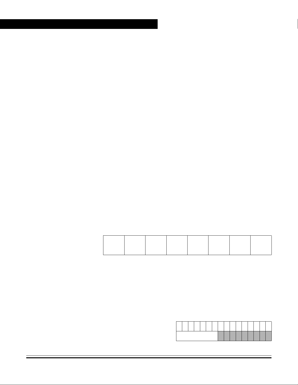
FLASH Memory
4.7 FLASH Protection
Due to the ability of the on-board charge pump to erase and program the
FLASH memory in the target application, provision is made to protect
pages of memory from unintentional erase or program operations due to
system malfunction. This protection is done by use of a FLASH block
protect register (FLBPR). The FLBPR determines the range of the
FLASH memory which is to be protected. The range of the protected
area starts from a location defined by FLBPR and ends to the bottom of
the FLASH memory ($FFFF). When the memory is protected, the HVEN
bit cannot be set in either erase or program operations.
Freescale Semiconductor, Inc.
nc...
I
cale Semiconductor,
Frees
NOTE: The mask option register ($FFCF) and the 48 bytes of user interrupt
vectors ($FFD0–$FFFF) are always protected, regardless of the value in
the FLASH block protect register. A mass erase is required to erase
these locations.
4.7.1 FLASH Block Protect Register
The FLASH block protect register is implemented as an 8-bit I/O register.
The value in this register determines the starting address of the
protected range within the FLASH memory.
Address: $FE09
Read:
Write:
Reset:00000000
Bit 7654321Bit 0
BPR7 BPR6 BPR5 BPR4 BPR3 BPR2 BPR1 BPR0
Figure 4-4. FLASH Block Protect Register (FLBPR)
BPR[7:0] — FLASH Block Protect Bits
BPR[7:1] represent bits [15:9] of a 16-bit memory address. Bits [8:0]
are logic 0’s.
16-bit memory address
Start address of FLASH block protect 000000000
BPR[7:1]
Data Sheet MC68HC908AP Family — Rev. 2.5
62 MOTOROLA
For More Information On This Product,
Go to: www.freescale.com
Freescale Semiconductor, Inc.
FLASH Memory
FLASH Protection
BPR0 is used only for BPR[7:0] = $FF, for no block protection.
The resultant 16-bit address is used for specifying the start address
of the FLASH memory for block protection. The FLASH is protected
from this start address to the end of FLASH memory, at $FFFF. With
this mechanism, the protect start address can be X000, X200, X400,
X0600, X800, XA00, XC00, or XE00 (at page boundaries — 512
bytes) within the FLASH memory.
Examples of protect start address:
Table 4-1 FLASH Block Protect Range
BPR[7:0] Protected Range
nc...
I
$00 to $09 The entire FLASH memory is protected.
cale Semiconductor,
Frees
$0A or $0B
(0000 101x)
$0C or $0D
(0000 110x)
and so on...
$FA or $FB
(1111 1101x)
$FC or $FD or $FE $FFCF to $FFFF
$FF The entire FLASH memory is NOT protected.
Notes:
1. Except for the mask option register ($FFCF) and
the 48-byte user vectors ($FFD0–$FFFF). These FLASH locations are always protected.
$0A00 to $FFFF
$0C00 to $FFFF
$FA00 to $FFFF
(1)
MC68HC908AP Family — Rev. 2.5 Data Sheet
MOTOROLA 63
For More Information On This Product,
Go to: www.freescale.com

Freescale Semiconductor, Inc.
FLASH Memory
nc...
I
cale Semiconductor,
Frees
Data Sheet MC68HC908AP Family — Rev. 2.5
64 MOTOROLA
For More Information On This Product,
Go to: www.freescale.com

Freescale Semiconductor, Inc.
Data Sheet – MC68HC908AP Family
Section 5. Configuration & Mask Option Registers
5.1 Introduction
This section describes the configuration registers, CONFIG1 and
CONFIG2; and the mask option register, MOR.
(CONFIG & MOR)
nc...
I
cale Semiconductor,
Frees
The configuration registers enable or disable these options:
• Computer operating properly module (COP)
• COP timeout period (218 – 24 or 213 – 24 ICLK cycles)
• Low-voltage inhibit (LVI) on V
• LVI on V
• LVI module reset
• LVI module in stop mode
• STOP instruction
• Stop mode recovery time (32 ICLK or 4096 ICLK cycles)
• Oscillator (internal, RC, and crystal) during stop mode
• Serial communications interface clock source (CGMXCLK or f
The mask option register selects one of the following oscillator options:
REG
DD
BUS
)
• Internal oscillator
• RC oscillator
• Crystal oscillator
MC68HC908AP Family — Rev. 2.5 Data Sheet
MOTOROLA 65
For More Information On This Product,
Go to: www.freescale.com

Freescale Semiconductor, Inc.
Configuration & Mask Option Registers
Addr.Register Name Bit 7654321Bit 0
nc...
I
cale Semiconductor,
Frees
Configuration Register 2
$001D
$001F
$FFCF
† One-time writable register after each reset.
#
MOR is a non-volatile FLASH register; write by programming.
Configuration Register 1
Mask-Option-Register
(CONFIG2)
(CONFIG1)
(MOR)
Read:
†
Write:
Reset:00000000
Read:
Write:
†
Reset:00000000
Read:
#
Write:
Erased:
STOP_
ICLKDIS
COPRS LVISTOP LVIRSTD LVIPWRD
OSCSEL1OSCSEL0RRRRRR
Figure 5-1. CONFIG and MOR Registers Summary
5.2 Functional Description
The configuration registers and the mask option register are used in the
initialization of various options. These two types of registers are
configured differently:
• Configuration registers — Write-once registers after reset
• Mask option register — FLASH register (write by programming)
The configuration registers can be written once after each reset. All of
the configuration register bits are cleared during reset. Since the various
options affect the operation of the MCU, it is recommended that these
registers be written immediately after reset. The configuration registers
are located at $001D and $001F. The configuration registers may be
read at anytime.
STOP_
RCLKEN
11111111
= Unimplemented R = Reserved
STOP_
XCLKEN
OSCCLK1 OSCCLK0
LVIREGD SSREC STOP COPD
00
SCIBD-
SRC
NOTE: The CONFIG registers are not in the FLASH memory but are special
registers containing one-time writable latches after each reset. Upon a
reset, the CONFIG registers default to predetermined settings as shown
in Figure 5-2 and Figure 5-3.
Data Sheet MC68HC908AP Family — Rev. 2.5
66 MOTOROLA
For More Information On This Product,
Go to: www.freescale.com

Freescale Semiconductor, Inc.
The mask option register (MOR) is used for selecting one of the three
clock options for the MCU. The MOR is a byte located in FLASH
memory, and is written to by a FLASH programming routine.
Configuration & Mask Option Registers (CONFIG & MOR)
5.3 Configuration Register 1 (CONFIG1)
Address: $001F
Bit 7654321Bit 0
Configuration Register 1 (CONFIG1)
Read:
Write:
nc...
I
Reset:00000000
COPRS — COP Rate Select Bit
LVISTOP — LVI Enable in Stop Mode Bit
cale Semiconductor,
NOTE: If LVISTOP=0, set LVIRSTD= 1 before entering stop mode.
COPRS LVISTOP LVIRSTD LVIPWRD LVIREGD SSREC STOP COPD
Figure 5-2. Configuration Register 1 (CONFIG1)
COPRS selects the COP time out period. Reset clears COPRS. (See
Section 21. Computer Operating Properly (COP).)
13
1 = COP time out period = 2
0 = COP time out period = 2
When the LVIPWRD or LVIREGD bit is clear, setting the LVISTOP bit
enables the LVI to operate during stop mode. Reset clears LVISTOP.
(See Section 22. Low-Voltage Inhibit (LVI).)
1 = LVI enabled during stop mode
0 = LVI disabled during stop mode
– 24 ICLK cycles
18
– 24 ICLK cycles
Frees
LVIRSTD — LVI Reset Disable Bit
LVIRSTD disables the reset signal from the LVI module. (See
Section 22. Low-Voltage Inhibit (LVI).)
1 = LVI module resets disabled
0 = LVI module resets enabled
MC68HC908AP Family — Rev. 2.5 Data Sheet
MOTOROLA 67
For More Information On This Product,
Go to: www.freescale.com

Freescale Semiconductor, Inc.
Configuration & Mask Option Registers
nc...
I
cale Semiconductor,
Frees
LVIPWRD — V
LVIPWRD disables the V
Voltage Inhibit (LVI).)
1 = V
DD
0 = VDD LVI circuit enabled
LVIREGD — V
LVIREGD disables the V
Voltage Inhibit (LVI).)
1 = V
REG
0 = V
REG
LVI Circuit Disable Bit
DD
LVI circuit. (See Section 22. Low-
DD
LVI circuit disabled
LVI Circuit Disable Bit
REG
LVI circuit. (See Section 22. Low-
REG
LVI circuit disabled
LVI circuit enabled
NOTE: If LVIPWRD=1 and LVIREGD= 1, set LVIRSTD=1 before entering stop
mode.
SSREC — Short Stop Recovery Bit
SSREC enables the CPU to exit stop mode with a delay of 32 ICLK
cycles instead of a 4096 ICLK cycle delay.
1 = Stop mode recovery after 32 ICLK cycles
0 = Stop mode recovery after 4096 ICLK cycles
NOTE: Exiting stop mode by pulling reset will result in the long stop recovery.
If using an external crystal oscillator, do not set the SSREC bit.
When the LVI is disabled in stop mode (LVISTOP=0), the system
stabilization time for long stop recovery (4096 ICLK cycles) gives a delay
longer than the LVI’s turn-on time. There is no period where the MCU is
not protected from a low power condition. However, when using the
short stop recovery configuration option, the 32 ICLK delay is less than
the LVI’s turn-on time and there exists a period in start-up where the LVI
is not protecting the MCU.
STOP — STOP Instruction Enable Bit
STOP enables the STOP instruction.
1 = STOP instruction enabled
0 = STOP instruction treated as illegal opcode
Data Sheet MC68HC908AP Family — Rev. 2.5
68 MOTOROLA
For More Information On This Product,
Go to: www.freescale.com

Freescale Semiconductor, Inc.
Configuration & Mask Option Registers (CONFIG & MOR)
COPD — COP Disable Bit
COPD disables the COP module. (See Section 21. Computer
Operating Properly (COP).)
1 = COP module disabled
0 = COP module enabled
5.4 Configuration Register 2 (CONFIG2)
Address: $001D
Bit 7654321Bit 0
Configuration Register 2 (CONFIG2)
nc...
I
cale Semiconductor,
Frees
Read:
Write:
Reset:00000000
STOP_
ICLKDIS
STOP_
RCLKEN
STOP_
XCLKEN
OSCCLK1 OSCCLK0
00
SCIBDSRC
Figure 5-3. Configuration Register 2 (CONFIG2)
STOP_ICLKDIS — Internal Oscillator Stop Mode Disable
STOP_ICLKDIS disables the internal oscillator during stop mode.
Setting the STOP_ICLKDIS bit disables the oscillator during stop
mode. (See Section 7. Oscillator (OSC).)
Reset clears this bit.
1 = Internal oscillator disabled during stop mode
0 = Internal oscillator enabled to operate during stop mode
STOP_RCLKEN — RC Oscillator Stop Mode Enable Bit
STOP_RCLKEN enables the RC oscillator to continue operating
during stop mode. Setting the STOP_RCLKEN bit allows the
oscillator to operate continuously even during stop mode. This is
useful for driving the timebase module to allow it to generate periodic
wake up while in stop mode. (See Section 7. Oscillator (OSC).)
Reset clears this bit.
1 = RC oscillator enabled to operate during stop mode
0 = RC oscillator disabled during stop mode
MC68HC908AP Family — Rev. 2.5 Data Sheet
MOTOROLA 69
For More Information On This Product,
Go to: www.freescale.com

Freescale Semiconductor, Inc.
Configuration & Mask Option Registers
STOP_XCLKEN — X-tal Oscillator Stop Mode Enable Bit
STOP_XCLKEN enables the crystal (x-tal) oscillator to continue
operating during stop mode. Setting the STOP_XCLKEN bit allows
the x-tal oscillator to operate continuously even during stop mode.
This is useful for driving the timebase module to allow it to generate
periodic wake up while in stop mode. (See Section 7. Oscillator
(OSC).) Reset clears this bit.
1 = X-tal oscillator enabled to operate during stop mode
0 = X-tal oscillator disabled during stop mode
OSCCLK1, OSCCLK0 — Oscillator Output Control Bits
nc...
I
cale Semiconductor,
Frees
OSCCLK1 and OSCCLK0 select which oscillator output to be driven
out as OSCCLK to the timebase module (TBM). Reset clears these
two bits.
OSCCLK1 OSCCLK0 Timebase Clock Source
0 0 Internal oscillator (ICLK)
SCIBDSRC — SCI Baud Rate Clock Source
SCIBDSRC selects the clock source used for the standard SCI
module (non-infrared SCI). The setting of this bit affects the frequency
at which the SCI operates.
0 1 RC oscillator (RCCLK)
1 0 X-tal oscillator (XTAL)
1 1 Not used
1 = Internal data bus clock, f
0 = Oscillator clock, CGMXCLK, is used as clock source for SCI
, is used as clock source for SCI
BUS
Data Sheet MC68HC908AP Family — Rev. 2.5
70 MOTOROLA
For More Information On This Product,
Go to: www.freescale.com

Freescale Semiconductor, Inc.
5.5 Mask Option Register (MOR)
The mask option register (MOR) is used for selecting one of the three
clock options for the MCU. The MOR is a byte located in FLASH
memory, and is written to by a FLASH programming routine.
Address: $FFCF
Bit 7654321Bit 0
Read:
OSCSEL1OSCSEL0RRRRRR
Write:
Reset: Unaffected by reset
Configuration & Mask Option Registers (CONFIG & MOR)
Mask Option Register (MOR)
nc...
I
cale Semiconductor,
Frees
Erased:11111111
R=Reserved
Figure 5-4. Mask Option Register (MOR)
OSCSEL1, OSCSEL0 — Oscillator Selection Bits
OSCSEL1 and OSCSEL0 select which oscillator is used for the MCU
CGMXCLK clock. The erase state of these two bits is logic 1. These
bits are unaffected by reset. (See Table 5-1).
Bits 5–0 — Should be left as 1’s.
Table 5-1. CGMXCLK Clock Selection
OSCSEL1 OSCSEL0 CGMXCLK OSC2 pin Comments
0 0 — — Not used
01ICLKf
1 0 RCCLK f
BUS
BUS
Internal oscillator generates the CGMXCLK.
RC oscillator generates the CGMXCLK.
Internal oscillator is available after each POR
or reset.
Inverting
11X-TAL
output of
XTAL
X-tal oscillator generates the CGMXCLK.
Internal oscillator is available after each POR
or reset.
NOTE: The internal oscillator is a free running oscillator and is available after
each POR or reset. It is turned-off in stop mode by setting the
STOP_ICLKDIS bit in CONFIG2.
MC68HC908AP Family — Rev. 2.5 Data Sheet
MOTOROLA 71
For More Information On This Product,
Go to: www.freescale.com

Freescale Semiconductor, Inc.
Configuration & Mask Option Registers
nc...
I
cale Semiconductor,
Frees
Data Sheet MC68HC908AP Family — Rev. 2.5
72 MOTOROLA
For More Information On This Product,
Go to: www.freescale.com

Freescale Semiconductor, Inc.
Data Sheet – MC68HC908AP Family
Section 6. Central Processor Unit (CPU)
6.1 Introduction
The M68HC08 CPU (central processor unit) is an enhanced and fully
object-code-compatible version of the M68HC05 CPU. The CPU08
Reference Manual (Motorola document order number CPU08RM/AD)
nc...
I
contains a description of the CPU instruction set, addressing modes,
and architecture.
cale Semiconductor,
Frees
6.2 Features
Feature of the CPU include:
• Object code fully upward-compatible with M68HC05 Family
• 16-bit stack pointer with stack manipulation instructions
• 16-Bit index register with X-register manipulation instructions
• 8-MHz CPU internal bus frequency
• 64-Kbyte program/data memory space
• 16 addressing modes
• Memory-to-memory data moves without using accumulator
• Fast 8-bit by 8-bit multiply and 16-bit by 8-bit divide instructions
• Enhanced binary-coded decimal (BCD) data handling
• Modular architecture with expandable internal bus definition for
extension of addressing range beyond 64-Kbytes
• Low-power stop and wait modes
MC68HC908AP Family — Rev. 2.5 Data Sheet
MOTOROLA 73
For More Information On This Product,
Go to: www.freescale.com
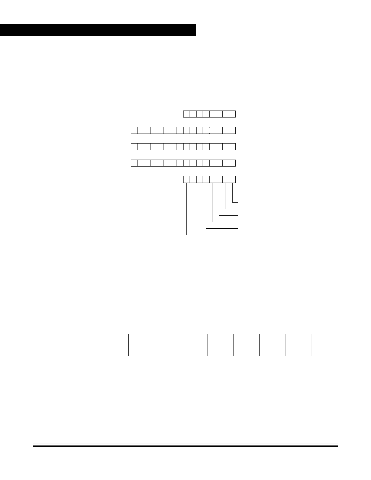
Freescale Semiconductor, Inc.
Central Processor Unit (CPU)
6.3 CPU Registers
Figure 6-1 shows the five CPU registers. CPU registers are not part of
the memory map.
nc...
I
cale Semiconductor,
Frees
6.3.1 Accumulator
7
15
H X
15
15
70
V11H I NZC
0
ACCUMULATOR (A)
0
INDEX REGISTER (H:X)
0
STACK POINTER (SP)
0
PROGRAM COUNTER (PC)
CONDITION CODE REGISTER (CCR)
CARRY/BORROW FLAG
ZERO FLAG
NEGATIVE FLAG
INTERRUPT MASK
HALF-CARRY FLAG
TWO’S COMPLEMENT OVERFLOW FLAG
Figure 6-1. CPU Registers
The accumulator is a general-purpose 8-bit register. The CPU uses the
accumulator to hold operands and the results of arithmetic/logic
operations.
Bit 7654321Bit 0
Read:
Write:
Reset: Unaffected by reset
Figure 6-2. Accumulator (A)
Data Sheet MC68HC908AP Family — Rev. 2.5
74 MOTOROLA
For More Information On This Product,
Go to: www.freescale.com

6.3.2 Index Register
Freescale Semiconductor, Inc.
Central Processor Unit (CPU)
CPU Registers
The 16-bit index register allows indexed addressing of a 64K-byte
memory space. H is the upper byte of the index register, and X is the
lower byte. H:X is the concatenated 16-bit index register.
In the indexed addressing modes, the CPU uses the contents of the
index register to determine the conditional address of the operand.
The index register can serve also as a temporary data storage location.
nc...
I
cale Semiconductor,
Frees
6.3.3 Stack Pointer
Bit
1413121110987654321
15
Read:
Write:
Reset:00000000XXXXXXXX
X = Indeterminate
Bit
0
Figure 6-3. Index Register (H:X)
The stack pointer is a 16-bit register that contains the address of the next
location on the stack. During a reset, the stack pointer is preset to
$00FF. The reset stack pointer (RSP) instruction sets the least
significant byte to $FF and does not affect the most significant byte. The
stack pointer decrements as data is pushed onto the stack and
increments as data is pulled from the stack.
In the stack pointer 8-bit offset and 16-bit offset addressing modes, the
stack pointer can function as an index register to access data on the
stack. The CPU uses the contents of the stack pointer to determine the
conditional address of the operand.
Bit
1413121110987654321
15
Read:
Write:
Reset:0000000011111111
Bit
0
Figure 6-4. Stack Pointer (SP)
MC68HC908AP Family — Rev. 2.5 Data Sheet
MOTOROLA 75
For More Information On This Product,
Go to: www.freescale.com

Freescale Semiconductor, Inc.
Central Processor Unit (CPU)
NOTE: The location of the stack is arbitrary and may be relocated anywhere in
RAM. Moving the SP out of page 0 ($0000 to $00FF) frees direct
address (page 0) space. For correct operation, the stack pointer must
point only to RAM locations.
6.3.4 Program Counter
The program counter is a 16-bit register that contains the address of the
next instruction or operand to be fetched.
Normally, the program counter automatically increments to the next
nc...
I
sequential memory location every time an instruction or operand is
fetched. Jump, branch, and interrupt operations load the program
counter with an address other than that of the next sequential location.
cale Semiconductor,
Frees
During reset, the program counter is loaded with the reset vector
address located at $FFFE and $FFFF. The vector address is the
address of the first instruction to be executed after exiting the reset state.
Bit
1413121110987654321
15
Read:
Write:
Reset: Loaded with Vector from $FFFE and $FFFF
Figure 6-5. Program Counter (PC)
Bit
0
Data Sheet MC68HC908AP Family — Rev. 2.5
76 MOTOROLA
For More Information On This Product,
Go to: www.freescale.com

Freescale Semiconductor, Inc.
6.3.5 Condition Code Register
The 8-bit condition code register contains the interrupt mask and five
flags that indicate the results of the instruction just executed. Bits 6 and
5 are set permanently to logic 1. The following paragraphs describe the
functions of the condition code register.
Central Processor Unit (CPU)
CPU Registers
Bit 7654321Bit 0
nc...
I
cale Semiconductor,
Frees
Read:
Write:
Reset:
V11H I NZC
X1 1 X1XXX
X = Indeterminate
Figure 6-6. Condition Code Register (CCR)
V — Overflow Flag
The CPU sets the overflow flag when a two's complement overflow
occurs. The signed branch instructions BGT, BGE, BLE, and BLT use
the overflow flag.
1 = Overflow
0 = No overflow
H — Half-Carry Flag
The CPU sets the half-carry flag when a carry occurs between
accumulator bits 3 and 4 during an add-without-carry (ADD) or addwith-carry (ADC) operation. The half-carry flag is required for binarycoded decimal (BCD) arithmetic operations. The DAA instruction
uses the states of the H and C flags to determine the appropriate
correction factor.
1 = Carry between bits 3 and 4
0 = No carry between bits 3 and 4
MC68HC908AP Family — Rev. 2.5 Data Sheet
MOTOROLA 77
For More Information On This Product,
Go to: www.freescale.com

Freescale Semiconductor, Inc.
Central Processor Unit (CPU)
I — Interrupt Mask
When the interrupt mask is set, all maskable CPU interrupts are
disabled. CPU interrupts are enabled when the interrupt mask is
cleared. When a CPU interrupt occurs, the interrupt mask is set
automatically after the CPU registers are saved on the stack, but
before the interrupt vector is fetched.
1 = Interrupts disabled
0 = Interrupts enabled
NOTE: To maintain M6805 Family compatibility, the upper byte of the index
register (H) is not stacked automatically. If the interrupt service routine
modifies H, then the user must stack and unstack H using the PSHH and
nc...
I
PULH instructions.
cale Semiconductor,
Frees
After the I bit is cleared, the highest-priority interrupt request is
serviced first.
A return-from-interrupt (RTI) instruction pulls the CPU registers from
the stack and restores the interrupt mask from the stack. After any
reset, the interrupt mask is set and can be cleared only by the clear
interrupt mask software instruction (CLI).
N — Negative Flag
The CPU sets the negative flag when an arithmetic operation, logic
operation, or data manipulation produces a negative result, setting
bit 7 of the result.
1 = Negative result
0 = Non-negative result
Z — Zero Flag
The CPU sets the zero flag when an arithmetic operation, logic
operation, or data manipulation produces a result of $00.
1 = Zero result
0 = Non-zero result
Data Sheet MC68HC908AP Family — Rev. 2.5
78 MOTOROLA
For More Information On This Product,
Go to: www.freescale.com

Freescale Semiconductor, Inc.
C — Carry/Borrow Flag
The CPU sets the carry/borrow flag when an addition operation
produces a carry out of bit 7 of the accumulator or when a subtraction
operation requires a borrow. Some instructions — such as bit test and
branch, shift, and rotate — also clear or set the carry/borrow flag.
1 = Carry out of bit 7
0 = No carry out of bit 7
Central Processor Unit (CPU)
Arithmetic/Logic Unit (ALU)
6.4 Arithmetic/Logic Unit (ALU)
The ALU performs the arithmetic and logic operations defined by the
nc...
I
instruction set.
cale Semiconductor,
Frees
Refer to the CPU08 Reference Manual (Motorola document order
number CPU08RM/AD) for a description of the instructions and
addressing modes and more detail about the architecture of the CPU.
6.5 Low-Power Modes
The WAIT and STOP instructions put the MCU in low power-consumption
standby modes.
6.5.1 Wait Mode
The WAIT instruction:
• Clears the interrupt mask (I bit) in the condition code register,
• Disables the CPU clock.
enabling interrupts. After exit from wait mode by interrupt, the I bit
remains clear. After exit by reset, the I bit is set.
MC68HC908AP Family — Rev. 2.5 Data Sheet
MOTOROLA 79
For More Information On This Product,
Go to: www.freescale.com

Freescale Semiconductor, Inc.
Central Processor Unit (CPU)
6.5.2 Stop Mode
The STOP instruction:
• Clears the interrupt mask (I bit) in the condition code register,
enabling external interrupts. After exit from stop mode by external
interrupt, the I bit remains clear. After exit by reset, the I bit is set.
• Disables the CPU clock.
After exiting stop mode, the CPU clock begins running after the oscillator
stabilization delay.
nc...
I
6.6 CPU During Break Interrupts
cale Semiconductor,
Frees
If the break module is enabled, a break interrupt causes the CPU to
execute the software interrupt instruction (SWI) at the completion of the
current CPU instruction. (See Section 23. Break Module (BRK).) The
program counter vectors to $FFFC–$FFFD ($FEFC–$FEFD in monitor
mode).
A return-from-interrupt instruction (RTI) in the break routine ends the
break interrupt and returns the MCU to normal operation if the break
interrupt has been deasserted.
6.7 Instruction Set Summary
Table 6-1 provides a summary of the M68HC08 instruction set.
6.8 Opcode Map
The opcode map is provided in Table 6-2.
Data Sheet MC68HC908AP Family — Rev. 2.5
80 MOTOROLA
For More Information On This Product,
Go to: www.freescale.com

Freescale Semiconductor, Inc.
Central Processor Unit (CPU)
Opcode Map
Table 6-1. Instruction Set Summary (Sheet 1 of 8)
Effect on
Source
Form
ADC #opr
ADC opr
ADC opr
ADC opr,X
ADC opr,X
ADC ,X
ADC opr,SP
ADC opr,SP
ADD #opr
ADD opr
ADD opr
nc...
I
ADD opr,X
ADD opr,X
ADD ,X
ADD opr,SP
ADD opr,SP
AIS #opr Add Immediate Value (Signed) to SP SP ← (SP) + (16 « M) ––––––IMM A7 ii 2
Add with Carry A ← (A) + (M) + (C) RR– RRR
Add without Carry A ← (A) + (M) RR– RRR
Operation Description
CCR
VH I NZC
IMM
DIR
EXT
IX2
IX1
IX
SP1
SP2
IMM
DIR
EXT
IX2
IX1
IX
SP1
SP2
Address
Mode
A9
B9
C9
D9
E9
F9
9EE9
9ED9
AB
BB
CB
DB
EB
FB
9EEB
9EDB
Opcode
ii
dd
hh ll
ee ff
ff
ff
ee ff
ii
dd
hh ll
ee ff
ff
ff
ee ff
Operand
Cycles
2
3
4
4
3
2
4
5
2
3
4
4
3
2
4
5
cale Semiconductor,
Frees
AIX #opr Add Immediate Value (Signed) to H:X H:X ← (H:X) + (16 « M) ––––––IMM AF ii 2
2
ii
AND #opr
AND opr
AND opr
AND opr,X
AND opr,X
AND ,X
AND opr,SP
AND opr,SP
ASL opr
ASLA
ASLX
ASL opr,X
ASL ,X
ASL opr,SP
ASR opr
ASRA
ASRX
ASR opr,X
ASR opr,X
ASR opr,SP
BCC rel Branch if Carry Bit Clear PC ← (PC) + 2 + rel ? (C) = 0 – – – – – – REL 24 rr 3
BCLR n, opr Clear Bit n in M Mn ← 0 ––––––
Logical AND A ← (A) & (M) 0 – – RR–
Arithmetic Shift Left
(Same as LSL)
Arithmetic Shift Right R ––RRR
C
b7
b7
0
b0
C
b0
R ––RRR
IMM
DIR
EXT
IX2
IX1
IX
SP1
SP2
DIR
INH
INH
IX1
IX
SP1
DIR
INH
INH
IX1
IX
SP1
DIR (b0)
DIR (b1)
DIR (b2)
DIR (b3)
DIR (b4)
DIR (b5)
DIR (b6)
DIR (b7)
A4
B4
C4
D4
E4
F4
9EE4
9ED4
38
48
58
68
78
9E68
37
47
57
67
77
9E67
11
13
15
17
19
1B
1D
1F
dd
hh ll
ee ff
ff
ff
ee ff
dd
ff
ff
dd
ff
ff
dd
dd
dd
dd
dd
dd
dd
dd
3
4
4
3
2
4
5
4
1
1
4
3
5
4
1
1
4
3
5
4
4
4
4
4
4
4
4
MC68HC908AP Family — Rev. 2.5 Data Sheet
MOTOROLA 81
For More Information On This Product,
Go to: www.freescale.com

Freescale Semiconductor, Inc.
Central Processor Unit (CPU)
Table 6-1. Instruction Set Summary (Sheet 2 of 8)
Effect on
Source
Form
BCS rel Branch if Carry Bit Set (Same as BLO) PC ← (PC) + 2 + rel ? (C) = 1 ––––––REL 25 rr 3
BEQ rel Branch if Equal PC ← (PC) + 2 + rel ? (Z) = 1 ––––––REL 27 rr 3
Operation Description
CCR
VH I NZC
Address
Mode
Opcode
Operand
Cycles
nc...
I
cale Semiconductor,
Frees
BGE opr
BGT opr
BHCC rel Branch if Half Carry Bit Clear PC ← (PC) + 2 + rel ? (H) = 0 ––––––REL 28 rr 3
BHCS rel Branch if Half Carry Bit Set PC ← (PC) + 2 + rel ? (H) = 1 ––––––REL 29 rr 3
BHI rel Branch if Higher PC ← (PC) + 2 + rel ? (C) | (Z) = 0 – – – – – – REL 22 rr 3
BHS rel
BIH rel Branch if IRQ
BIL rel Branch if IRQ
BIT #opr
BIT opr
BIT opr
BIT opr,X
BIT opr,X
BIT ,X
BIT opr,SP
BIT opr,SP
BLE opr
BLO rel Branch if Lower (Same as BCS) PC ← (PC) + 2 + rel ? (C) = 1 ––––––REL 25 rr 3
BLS rel Branch if Lower or Same PC ← (PC) + 2 + rel ? (C) | (Z) = 1 – – – – – – REL 23 rr 3
BLT opr Branch if Less Than (Signed Operands) PC ← (PC) + 2 + rel ? (N ⊕ V) =1 ––––––REL 91 rr 3
BMC rel Branch if Interrupt Mask Clear PC ← (PC) + 2 + rel ? (I) = 0 ––––––REL 2C rr 3
BMI rel Branch if Minus PC ← (PC) + 2 + rel ? (N) = 1 ––––––REL 2B rr 3
BMS rel Branch if Interrupt Mask Set PC ← (PC) + 2 + rel ? (I) = 1 ––––––REL 2D rr 3
Branch if Greater Than or Equal To
(Signed Operands)
Branch if Greater Than (Signed
Operands)
Branch if Higher or Same
(Same as BCC)
Pin High PC ← (PC) + 2 + rel ? IRQ = 1 ––––––REL 2F rr 3
Pin Low PC ← (PC) + 2 + rel ? IRQ = 0 ––––––REL 2E rr 3
Bit Test (A) & (M) 0 – – RR –
Branch if Less Than or Equal To
(Signed Operands)
PC ← (PC) + 2 + rel ? (N ⊕ V) = 0 ––––––REL 90 rr 3
PC ← (PC) + 2 + rel ? (Z) | (N ⊕ V) = 0
PC ← (PC) + 2 + rel ? (C) = 0 ––––––REL 24 rr 3
PC ← (PC) + 2 + rel ? (Z) | (N ⊕ V) = 1
––––––REL 92 rr 3
IMM
DIR
EXT
IX2
IX1
IX
SP1
SP2
––––––REL 93 rr 3
A5
B5
C5
D5
E5
F5
9EE5
9ED5
ii
dd
hh ll
ee ff
ff
ff
ee ff
2
3
4
4
3
2
4
5
BNE rel Branch if Not Equal PC ← (PC) + 2 + rel ? (Z) = 0 ––––––REL 26 rr 3
BPL rel Branch if Plus PC ← (PC) + 2 + rel ? (N) = 0 ––––––REL 2A rr 3
BRA rel Branch Always PC ← (PC) + 2 + rel ––––––REL 20 rr 3
Data Sheet MC68HC908AP Family — Rev. 2.5
82 MOTOROLA
For More Information On This Product,
Go to: www.freescale.com

Freescale Semiconductor, Inc.
Central Processor Unit (CPU)
Opcode Map
Table 6-1. Instruction Set Summary (Sheet 3 of 8)
Effect on
Source
Form
BRCLR n,opr,rel Branch if Bit n in M Clear PC ← (PC) + 3 + rel ? (Mn) = 0 –––––R
BRN rel Branch Never PC ← (PC) + 2 ––––––REL 21 rr 3
nc...
I
BRSET n,opr,rel Branch if Bit n in M Set PC ← (PC) + 3 + rel ? (Mn) = 1 –––––R
Operation Description
CCR
VH I NZC
Address
Mode
DIR (b0)
DIR (b1)
DIR (b2)
DIR (b3)
DIR (b4)
DIR (b5)
DIR (b6)
DIR (b7)
DIR (b0)
DIR (b1)
DIR (b2)
DIR (b3)
DIR (b4)
DIR (b5)
DIR (b6)
DIR (b7)
01
03
05
07
09
0B
0D
0F
00
02
04
06
08
0A
0C
0E
Opcode
dd rr
dd rr
dd rr
dd rr
dd rr
dd rr
dd rr
dd rr
dd rr
dd rr
dd rr
dd rr
dd rr
dd rr
dd rr
dd rr
Operand
Cycles
5
5
5
5
5
5
5
5
5
5
5
5
5
5
5
5
cale Semiconductor,
Frees
DIR (b0)
DIR (b1)
DIR (b2)
BSET n,opr Set Bit n in M Mn ← 1 ––––––
PC ← (PC) + 2; push (PCL)
BSR rel Branch to Subroutine
CBEQ opr,rel
CBEQA #opr,rel
CBEQX #opr,rel
CBEQ opr,X+,rel
CBEQ X+,rel
CBEQ opr,SP,rel
CLC Clear Carry Bit C ← 0 –––––0INH 98 1
CLI Clear Interrupt Mask I ← 0 ––0–––INH 9A 2
CLR opr
CLRA
CLRX
CLRH
CLR opr,X
CLR ,X
CLR opr,SP
Compare and Branch if Equal
Clear
SP ← (SP) – 1; push (PCH)
SP ← (SP) – 1
PC ← (PC) + rel
PC ← (PC) + 3 + rel ? (A) – (M) = $00
PC ← (PC) + 3 + rel ? (A) – (M) = $00
PC ← (PC) + 3 + rel ? (X) – (M) = $00
PC ← (PC) + 3 + rel ? (A) – (M) = $00
PC ← (PC) + 2 + rel ? (A) – (M) = $00
PC ← (PC) + 4 + rel ? (A) – (M) = $00
M ← $00
A ← $00
X ← $00
H ← $00
M ← $00
M ← $00
M ← $00
––––––REL AD rr 4
––––––
0––01–
DIR (b3)
DIR (b4)
DIR (b5)
DIR (b6)
DIR (b7)
DIR
IMM
IMM
IX1+
IX+
SP1
DIR
INH
INH
INH
IX1
IX
SP1
10
12
14
16
18
1A
1C
1E
31
41
51
61
71
9E61
3F
4F
5F
8C
6F
7F
9E6F
dd
dd
dd
dd
dd
dd
dd
dd
dd rr
ii rr
ii rr
ff rr
rr
ff rr
dd
ff
ff
4
4
4
4
4
4
4
4
5
4
4
5
4
6
3
1
1
1
3
2
4
MC68HC908AP Family — Rev. 2.5 Data Sheet
MOTOROLA 83
For More Information On This Product,
Go to: www.freescale.com

Freescale Semiconductor, Inc.
Central Processor Unit (CPU)
Table 6-1. Instruction Set Summary (Sheet 4 of 8)
Effect on
Source
Form
CMP #opr
CMP opr
CMP opr
CMP opr,X
CMP opr,X
CMP ,X
CMP opr,SP
CMP opr,SP
COM opr
COMA
COMX
nc...
I
COM opr,X
COM ,X
COM opr,SP
Compare A with M (A) – (M) R ––RRR
Complement (One’s Complement)
Operation Description
M ← (M
) = $FF – (M)
A ← (A
) = $FF – (M)
X ← (X
) = $FF – (M)
M ← (M
) = $FF – (M)
M ← (M
) = $FF – (M)
M ← (M
) = $FF – (M)
CCR
VH I NZC
0––RR1
IMM
DIR
EXT
IX2
IX1
IX
SP1
SP2
DIR
INH
INH
IX1
IX
SP1
Address
Mode
A1
B1
C1
D1
E1
F1
9EE1
9ED1
33
43
53
63
73
9E63
Opcode
ii
dd
hh ll
ee ff
ff
ff
ee ff
dd
ff
ff
Operand
Cycles
2
3
4
4
3
2
4
5
4
1
1
4
3
5
cale Semiconductor,
Frees
CPHX #opr
CPHX opr
CPX #opr
CPX opr
CPX opr
CPX ,X
CPX opr,X
CPX opr,X
CPX opr,SP
CPX opr,SP
DAA Decimal Adjust A (A)
DBNZ opr,rel
DBNZA rel
DBNZX rel
DBNZ opr,X,rel
DBNZ X,rel
DBNZ opr,SP,rel
DEC opr
DECA
DECX
DEC opr,X
DEC ,X
DEC opr,SP
DIV Divide
EOR #opr
EOR opr
EOR opr
EOR opr,X
EOR opr,X
EOR ,X
EOR opr,SP
EOR opr,SP
Compare H:X with M (H:X) – (M:M + 1) R ––RRR
Compare X with M (X) – (M) R ––RRR
A ← (A) – 1 or M ← (M) – 1 or X ← (X) – 1
PC ← (PC) + 3 + rel ? (result) ≠ 0
PC ← (PC) + 2 + rel ? (result) ≠ 0
Decrement and Branch if Not Zero
Decrement
Exclusive OR M with A A ← (A ⊕ M) 0––RR–
PC ← (PC) + 2 + rel ? (result) ≠ 0
PC ← (PC) + 3 + rel ? (result) ≠ 0
PC ← (PC) + 2 + rel ? (result) ≠ 0
PC ← (PC) + 4 + rel ? (result) ≠ 0
10
M ← (M) – 1
A ← (A) – 1
X ← (X) – 1
M ← (M) – 1
M ← (M) – 1
M ← (M) – 1
A ← (H:A)/(X)
H ← Remainder
IMM
DIR
IMM
DIR
EXT
IX2
IX1
IX
SP1
SP2
U–– RRRINH 72 2
DIR
INH
––––––
R ––RR–
––––RRINH 52 7
INH
IX1
IX
SP1
DIR
INH
INH
IX1
IX
SP1
IMM
DIR
EXT
IX2
IX1
IX
SP1
SP2
6575ii ii+1dd3
ii
A3
dd
B3
hh ll
C3
ee ff
D3
ff
E3
F3
ff
9EE3
ee ff
9ED3
dd rr
3B
rr
4B
rr
5B
ff rr
6B
rr
7B
ff rr
9E6B
dd
3A
4A
5A
ff
6A
7A
9E6A
ff
ii
A8
dd
B8
hh ll
C8
ee ff
D8
ff
E8
F8
ff
9EE8
ee ff
9ED8
4
2
3
4
4
3
2
4
5
5
3
3
5
4
6
4
1
1
4
3
5
2
3
4
4
3
2
4
5
Data Sheet MC68HC908AP Family — Rev. 2.5
84 MOTOROLA
For More Information On This Product,
Go to: www.freescale.com

nc...
I
cale Semiconductor,
Frees
Source
Form
INC opr
INCA
INCX
INC opr,X
INC ,X
INC opr,SP
JMP opr
JMP opr
JMP opr,X
JMP opr,X
JMP ,X
JSR opr
JSR opr
JSR opr,X
JSR opr,X
JSR ,X
LDA #opr
LDA opr
LDA opr
LDA opr,X
LDA opr,X
LDA ,X
LDA opr,SP
LDA opr,SP
LDHX #opr
LDHX opr
LDX #opr
LDX opr
LDX opr
LDX opr,X
LDX opr,X
LDX ,X
LDX opr,SP
LDX opr,SP
LSL opr
LSLA
LSLX
LSL opr,X
LSL ,X
LSL opr,SP
Freescale Semiconductor, Inc.
Central Processor Unit (CPU)
Table 6-1. Instruction Set Summary (Sheet 5 of 8)
Effect on
Operation Description
M ← (M) + 1
A ← (A) + 1
Increment
Jump PC ← Jump Address ––––––
PC ← (PC) + n (n = 1, 2, or 3)
Jump to Subroutine
PC ← Unconditional Address
Load A from M A ← (M) 0––RR–
Load H:X from M H:X ← (M:M + 1) 0––RR–
Load X from M X ← (M) 0––RR–
Logical Shift Left
(Same as ASL)
X ← (X) + 1
M ← (M) + 1
M ← (M) + 1
M ← (M) + 1
Push (PCL); SP ← (SP) – 1
Push (PCH); SP ← (SP) – 1
C
b7
0
b0
CCR
VH I NZC
R ––RR–
––––––
R ––RRR
DIR
INH
INH
IX1
IX
SP1
DIR
EXT
IX2
IX1
IX
DIR
EXT
IX2
IX1
IX
IMM
DIR
EXT
IX2
IX1
IX
SP1
SP2
IMM
DIR
IMM
DIR
EXT
IX2
IX1
IX
SP1
SP2
DIR
INH
INH
IX1
IX
SP1
Opcode Map
Address
Mode
Opcode
Operand
dd
3C
4C
5C
ff
6C
7C
9E6C
ff
dd
BC
hh ll
CC
ee ff
DC
ff
EC
FC
dd
BD
hh ll
CD
ee ff
DD
ff
ED
FD
ii
A6
dd
B6
hh ll
C6
ee ff
D6
ff
E6
F6
ff
9EE6
ee ff
9ED6
4555ii jjdd3
ii
AE
dd
BE
hh ll
CE
ee ff
DE
ff
EE
FE
ff
9EEE
ee ff
9EDE
dd
38
48
58
ff
68
78
9E68
ff
Cycles
4
1
1
4
3
5
2
3
4
3
2
4
5
6
5
4
2
3
4
4
3
2
4
5
4
2
3
4
4
3
2
4
5
4
1
1
4
3
5
LSR opr
LSRA
LSRX
LSR opr,X
LSR ,X
LSR opr,SP
Logical Shift Right R ––0RR
b7
C0
b0
DIR
INH
INH
IX1
IX
SP1
34
44
54
64
74
9E64
dd
ff
ff
4
1
1
4
3
5
MC68HC908AP Family — Rev. 2.5 Data Sheet
MOTOROLA 85
For More Information On This Product,
Go to: www.freescale.com

Freescale Semiconductor, Inc.
Central Processor Unit (CPU)
Table 6-1. Instruction Set Summary (Sheet 6 of 8)
Effect on
Source
Form
MOV opr,opr
MOV opr,X+
MOV #opr,opr
MOV X+,opr
MUL Unsigned multiply X:A ← (X) × (A) –0–––0INH 42 5
NEG opr
NEGA
NEGX
NEG opr,X
NEG ,X
nc...
I
NEG opr,SP
NOP No Operation None – – – – – – INH 9D 1
Move
Negate (Two’s Complement)
Operation Description
(M)
Destination
H:X ← (H:X) + 1 (IX+D, DIX+)
M ← –(M) = $00 – (M)
A ← –(A) = $00 – (A)
X ← –(X) = $00 – (X)
M ← –(M) = $00 – (M)
M ← –(M) = $00 – (M)
← (M)
Source
CCR
VH I NZC
0––RR–
R ––RRR
DD
DIX+
IMD
IX+D
DIR
INH
INH
IX1
IX
SP1
Address
Mode
4E
5E
6E
7E
30
40
50
60
70
9E60
Opcode
dd dd
dd
ii dd
dd
dd
ff
ff
Operand
Cycles
5
4
4
4
4
1
1
4
3
5
cale Semiconductor,
Frees
NSA Nibble Swap A A ← (A[3:0]:A[7:4]) – – – – – – INH 62 3
ORA #opr
ORA opr
ORA opr
ORA opr,X
ORA opr,X
ORA ,X
ORA opr,SP
ORA opr,SP
PSHA Push A onto Stack Push (A); SP ← (SP) – 1 ––––––INH 87 2
PSHH Push H onto Stack Push (H); SP ← (SP) – 1 ––––––INH 8B 2
PSHX Push X onto Stack Push (X); SP ← (SP) – 1 ––––––INH 89 2
PULA Pull A from Stack SP ← (SP + 1); Pull (A) ––––––INH 86 2
PULH Pull H from Stack SP ← (SP + 1); Pull (H) ––––––INH 8A 2
PULX Pull X from Stack SP ← (SP + 1); Pull (X) ––––––INH 88 2
ROL opr
ROLA
ROLX
ROL opr,X
ROL ,X
ROL opr,SP
ROR opr
RORA
RORX
ROR opr,X
ROR ,X
ROR opr,SP
Inclusive OR A and M A ← (A) | (M) 0 – – RR
Rotate Left through Carry R ––RRR
Rotate Right through Carry R ––RRR
C
b7
b7
b0
C
b0
IMM
DIR
EXT
IX2
–
IX1
IX
SP1
SP2
DIR
INH
INH
IX1
IX
SP1
DIR
INH
INH
IX1
IX
SP1
AA
BA
CA
DA
EA
FA
9EEA
9EDA
39
49
59
69
79
9E69
36
46
56
66
76
9E66
ii
dd
hh ll
ee ff
ff
ff
ee ff
dd
ff
ff
dd
ff
ff
2
3
4
4
3
2
4
5
4
1
1
4
3
5
4
1
1
4
3
5
RSP Reset Stack Pointer SP ← $FF ––––––INH 9C 1
Data Sheet MC68HC908AP Family — Rev. 2.5
86 MOTOROLA
For More Information On This Product,
Go to: www.freescale.com

Freescale Semiconductor, Inc.
Central Processor Unit (CPU)
Opcode Map
Table 6-1. Instruction Set Summary (Sheet 7 of 8)
Effect on
Source
Form
RTI Return from Interrupt
RTS Return from Subroutine
SBC #opr
SBC opr
SBC opr
nc...
I
SBC opr,X
SBC opr,X
SBC ,X
SBC opr,SP
SBC opr,SP
SEC Set Carry Bit C ← 1 –––––1INH 99 1
Subtract with Carry A ← (A) – (M) – (C) R ––RRR
Operation Description
SP ← (SP) + 1; Pull (CCR)
SP ← (SP) + 1; Pull (A)
SP ← (SP) + 1; Pull (X)
SP ← (SP) + 1; Pull (PCH)
SP ← (SP) + 1; Pull (PCL)
SP ← SP + 1; Pull (PCH)
SP ← SP + 1; Pull (PCL)
CCR
VH I NZC
RRRRRRINH 80 7
––––––INH 81 4
IMM
DIR
EXT
IX2
IX1
IX
SP1
SP2
Address
Mode
A2
B2
C2
D2
E2
F2
9EE2
9ED2
Opcode
ii
dd
hh ll
ee ff
ff
ff
ee ff
Operand
2
3
4
4
3
2
4
5
Cycles
cale Semiconductor,
Frees
SEI Set Interrupt Mask I ← 1 ––1–––INH 9B 2
STA opr
STA opr
STA opr,X
STA opr,X
STA ,X
STA opr,SP
STA opr,SP
STHX opr Store H:X in M (M:M + 1) ← (H:X) 0 – – RR– DIR 35 dd 4
STOP Enable IRQ
STX opr
STX opr
STX opr,X
STX opr,X
STX ,X
STX opr,SP
STX opr,SP
SUB #opr
SUB opr
SUB opr
SUB opr,X
SUB opr,X
SUB ,X
SUB opr,SP
SUB opr,SP
Store A in M M ← (A) 0––RR–
Pin; Stop Oscillator I ← 0; Stop Oscillator – – 0 – – – INH 8E 1
Store X in M M ← (X) 0––RR–
Subtract A ← (A) – (M) R ––RRR
DIR
EXT
IX2
IX1
IX
SP1
SP2
DIR
EXT
IX2
IX1
IX
SP1
SP2
IMM
DIR
EXT
IX2
IX1
IX
SP1
SP2
B7
C7
D7
E7
F7
9EE7
9ED7
BF
CF
DF
EF
FF
9EEF
9EDF
A0
B0
C0
D0
E0
F0
9EE0
9ED0
dd
hh ll
ee ff
ff
ff
ee ff
dd
hh ll
ee ff
ff
ff
ee ff
ii
dd
hh ll
ee ff
ff
ff
ee ff
3
4
4
3
2
4
5
3
4
4
3
2
4
5
2
3
4
4
3
2
4
5
MC68HC908AP Family — Rev. 2.5 Data Sheet
MOTOROLA 87
For More Information On This Product,
Go to: www.freescale.com

nc...
I
cale Semiconductor,
Frees
Freescale Semiconductor, Inc.
Central Processor Unit (CPU)
Table 6-1. Instruction Set Summary (Sheet 8 of 8)
Effect on
Source
Form
SWI Software Interrupt
TAP Transfer A to CCR CCR ← (A) RRRRRRINH 84 2
TAX Transfer A to X X ← (A) ––––––INH 97 1
TPA Transfer CCR to A A ← (CCR) – – – – – – INH 85 1
TST opr
TSTA
TSTX
TST opr,X
TST ,X
TST opr,SP
TSX Transfer SP to H:X H:X ← (SP) + 1 ––––––INH 95 2
TXA Transfer X to A A ← (X) ––––––INH 9F 1
TXS Transfer H:X to SP (SP) ← (H:X) – 1 ––––––INH 94 2
A Accumulator n Any bit
C Carry/borrow bit opr Operand (one or two bytes)
CCR Condition code register PC Program counter
dd Direct address of operand PCH Program counter high byte
dd rr Direct address of operand and relative offset of branch instruction PCL Program counter low byte
DD Direct to direct addressing mode REL Relative addressing mode
DIR Direct addressing mode rel Relative program counter offset byte
DIX+ Direct to indexed with post increment addressing mode rr Relative program counter offset byte
ee ff High and low bytes of offset in indexed, 16-bit offset addressing SP1 Stack pointer, 8-bit offset addressing mode
EXT Extended addressing mode SP2 Stack pointer 16-bit offset addressing mode
ff Offset byte in indexed, 8-bit offset addressing SP Stack pointer
H Half-carry bit U Undefined
H Index register high byte V Overflow bit
hh ll High and low bytes of operand address in extended addressing X Index register low byte
I Interrupt mask Z Zero bit
ii Immediate operand byte & Logical AND
IMD Immediate source to direct destination addressing mode | Logical OR
IMM Immediate addressing mode
INH Inherent addressing mode ( ) Contents of
IX Indexed, no offset addressing mode –( ) Negation (two’s complement)
IX+ Indexed, no offset, post increment addressing mode # Immediate value
IX+D Indexed with post increment to direct addressing mode
IX1 Indexed, 8-bit offset addressing mode ← Loaded with
IX1+ Indexed, 8-bit offset, post increment addressing mode ? If
IX2 Indexed, 16-bit offset addressing mode : Concatenated with
M Memory location R Set or cleared
N Negative bit — Not affected
Test for Negative or Zero (A) – $00 or (X) – $00 or (M) – $00 0 – – RR–
Operation Description
PC ← (PC) + 1; Push (PCL)
SP ← (SP) – 1; Push (PCH)
SP ← (SP) – 1; Push (X)
SP ← (SP) – 1; Push (A)
SP ← (SP) – 1; Push (CCR)
SP ← (SP) – 1; I ← 1
PCH ← Interrupt Vector High Byte
PCL ← Interrupt Vector Low Byte
⊕ Logical EXCLUSIVE OR
« Sign extend
CCR
VH I NZC
––1–––INH 83 9
DIR
INH
INH
IX1
IX
SP1
Address
Mode
Opcode
3D
4D
5D
6D
7D
9E6D
dd
ff
ff
Operand
Cycles
3
1
1
3
2
4
Data Sheet MC68HC908AP Family — Rev. 2.5
88 MOTOROLA
For More Information On This Product,
Go to: www.freescale.com

Freescale Semiconductor, Inc.
Central Processor Unit (CPU)
Opcode Map
nc...
I
cale Semiconductor,
Frees
2
2
SUB
CMP
1IX
1IX
4
4
SUB
CMP
3SP1
3SP1
3
3
SUB
CMP
2IX1
2IX1
5
5
SUB
CMP
4SP2
4SP2
4
4
SUB
CMP
3IX2
3IX2
4
4
SUB
CMP
3EXT
3EXT
3
3
SUB
CMP
2DIR
2DIR
2
2
SUB
CMP
2IMM
2IMM
3
3
BLT
BGE
7
RTI
3
NEG
5
NEG
Table 6-2. Opcode Map
4
NEG
1
NEGX
1
NEGA
4
NEG
3
BRA
4
BSET0
2REL
1INH
1IX
3SP1
2IX1
1INH
1INH
2DIR
2REL
2DIR
4
4
6
5
4
4
5
3
4
2REL
RTS
1INH
CBEQ
2IX+
CBEQ
4SP1
CBEQ
3IX1+
CBEQX
3IMM
CBEQA
3IMM
CBEQ
3DIR
BRN
2REL
BCLR0
2DIR
2
4
3
5
4
4
3
2
3
2
3
7
5
3
4
SBC
1IX
SBC
3SP1
SBC
2IX1
SBC
4SP2
SBC
3IX2
SBC
3EXT
SBC
2DIR
SBC
2IMM
BGT
2REL
DAA
1INH
NSA
1INH
DIV
1INH
MUL
1INH
BHI
2REL
BSET1
2DIR
2
CPX
4
CPX
3
CPX
5
CPX
4
CPX
4
CPX
3
CPX
2
CPX
3
BLE
9
SWI
3
COM
5
COM
4
COM
1
COMX
1
COMA
4
COM
3
BLS
4
BCLR1
1IX
3SP1
2IX1
4SP2
3IX2
3EXT
2DIR
2IMM
2REL
1INH
1IX
3SP1
2IX1
1INH
1INH
2DIR
2REL
2DIR
2
4
3
5
4
4
3
2
2
2
3
5
4
1
1
4
3
4
AND
1IX
AND
3SP1
AND
2IX1
AND
4SP2
AND
3IX2
AND
3EXT
AND
2DIR
AND
2IMM
TXS
1INH
TA P
1INH
LSR
1IX
LSR
3SP1
LSR
2IX1
LSRX
1INH
LSRA
1INH
LSR
2DIR
BCC
2REL
BSET2
2DIR
2
BIT
4
BIT
3
BIT
5
BIT
4
BIT
4
BIT
3
BIT
2
BIT
2
TSX
1
TPA
4
CPHX
3
CPHX
4
LDHX
3
LDHX
4
STHX
3
BCS
4
BCLR2
1IX
3SP1
2IX1
4SP2
3IX2
3EXT
2DIR
2IMM
1INH
1INH
2DIR
3IMM
2DIR
3IMM
2DIR
2REL
2DIR
2
4
3
5
4
4
3
2
2
3
5
4
1
1
4
3
4
LDA
1IX
LDA
3SP1
LDA
2IX1
LDA
4SP2
LDA
3IX2
LDA
3EXT
LDA
2DIR
LDA
2IMM
PULA
1INH
ROR
1IX
ROR
3SP1
ROR
2IX1
RORX
1INH
RORA
1INH
ROR
2DIR
BNE
2REL
BSET3
2DIR
2
STA
4
STA
3
STA
5
STA
4
STA
4
STA
3
STA
2
AIS
1
TA X
2
PSHA
3
ASR
5
ASR
4
ASR
1
ASRX
1
ASRA
4
ASR
3
BEQ
4
BCLR3
1IX
3SP1
2IX1
4SP2
3IX2
3EXT
2DIR
2IMM
1INH
1INH
1IX
3SP1
2IX1
1INH
1INH
2DIR
2REL
2DIR
2
4
3
5
4
4
3
2
1
2
3
5
4
1
1
4
3
4
EOR
1IX
EOR
3SP1
EOR
2IX1
EOR
4SP2
EOR
3IX2
EOR
3EXT
EOR
2DIR
EOR
2IMM
CLC
1INH
PULX
1INH
LSL
1IX
LSL
3SP1
LSL
2IX1
LSLX
1INH
LSLA
1INH
LSL
2DIR
BHCC
2REL
BSET4
2DIR
2
ADC
4
ADC
3
ADC
5
ADC
4
ADC
4
ADC
3
ADC
2
ADC
1
SEC
2
PSHX
3
ROL
5
ROL
4
ROL
1
ROLX
1
ROLA
4
ROL
3
BHCS
4
BCLR4
1IX
3SP1
2IX1
4SP2
3IX2
3EXT
2DIR
2IMM
1INH
1INH
1IX
3SP1
2IX1
1INH
1INH
2DIR
2REL
2DIR
2
4
3
5
4
4
3
2
2
2
3
5
4
1
1
4
3
4
ORA
1IX
ORA
3SP1
ORA
2IX1
ORA
4SP2
ORA
3IX2
ORA
3EXT
ORA
2DIR
ORA
2IMM
CLI
1INH
PULH
1INH
DEC
1IX
DEC
3SP1
DEC
2IX1
DECX
1INH
DECA
1INH
DEC
2DIR
BPL
2REL
BSET5
2DIR
2
ADD
4
ADD
3
ADD
5
ADD
4
ADD
4
ADD
3
ADD
2
ADD
2
SEI
2
PSHH
4
DBNZ
6
DBNZ
5
DBNZ
3
DBNZX
3
DBNZA
5
DBNZ
3
BMI
4
BCLR5
1IX
3SP1
2IX1
4SP2
3IX2
3EXT
2DIR
2IMM
1INH
1INH
2IX
4SP1
3IX1
2INH
2INH
3DIR
2REL
2DIR
2
3
4
3
2
1
1
3
5
4
1
1
4
3
4
JMP
1IX
JMP
2IX1
JMP
3IX2
JMP
3EXT
JMP
2DIR
RSP
1INH
CLRH
1INH
INC
1IX
INC
3SP1
INC
2IX1
INCX
1INH
INCA
1INH
INC
2DIR
BMC
2REL
BSET6
2DIR
4
JSR
5
JSR
6
JSR
5
JSR
4
JSR
4
BSR
1
NOP
2
TST
4
TST
3
TST
1
TSTX
1
TSTA
3
TST
3
BMS
4
BCLR6
1IX
2IX1
3IX2
3EXT
2DIR
2REL
1INH
1IX
3SP1
2IX1
1INH
1INH
2DIR
2REL
2DIR
2
4
3
5
4
4
3
2
1
4
4
4
5
3
4
LDX
1IX
LDX
3SP1
LDX
2IX1
LDX
4SP2
LDX
3IX2
LDX
3EXT
LDX
2DIR
LDX
2IMM
*
STOP
1INH
MOV
2IX+D
MOV
3IMD
MOV
2DIX+
MOV
3DD
BIL
2REL
BSET7
2DIR
2
STX
4
STX
3
STX
5
STX
4
STX
4
STX
3
STX
2
AIX
1
TXA
1
WAIT
2
CLR
4
CLR
3
CLR
1
CLRX
1
CLRA
3
CLR
3
BIH
4
BCLR7
1IX
3SP1
2IX1
4SP2
3IX2
3EXT
2DIR
2IMM
1INH
1INH
1IX
3SP1
2IX1
1INH
1INH
2DIR
2REL
2DIR
Cycles
Opcode Mnemonic
Number of Bytes / Addressing Mode
5
0 High Byte of Opcode in Hexadecimal
BRSET0
3DIR
MSB
LSB
Low Byte of Opcode in Hexadecimal 0
DIR DIR REL DIR INH INH IX1 SP1 IX INH INH IMM DIR EXT IX2 SP2 IX1 SP1 IX
Bit Manipulation Branch Read-Modify-Write Control Register/Memory
01234569E6789ABCD9EDE9EEF
MSB
LSB
5
BRSET0
3DIR
0
5
BRCLR0
1
3DIR
BRSET1
3DIR
2
BRCLR1
3DIR
3
BRSET2
3DIR
4
5
BRCLR2
5
3DIR
5
BRSET3
3DIR
6
5
BRCLR3
7
3DIR
5
BRSET4
3DIR
8
5
BRCLR4
9
3DIR
5
BRSET5
3DIR
A
5
BRCLR5
B
3DIR
5
BRSET6
3DIR
C
5
BRCLR6
D
3DIR
5
BRSET7
3DIR
E
5
BRCLR7
F
3DIR
INH Inherent REL Relative SP1 Stack Pointer, 8-Bit Offset
IMM Immediate IX Indexed, No Offset SP2 Stack Pointer, 16-Bit Offset
DIR Direct IX1 Indexed, 8-Bit Offset IX+ Indexed, No Offset with
EXT Extended IX2 Indexed, 16-Bit Offset Post Increment
DD Direct-Direct IMD Immediate-Direct IX1+ Indexed, 1-Byte Offset with
IX+D Indexed-Direct DIX+ Direct-Indexed Post Increment
*Pre-byte for stack pointer indexed instructions
5
5
5
MC68HC908AP Family — Rev. 2.5 Data Sheet
MOTOROLA Central Processor Unit (CPU) 89
For More Information On This Product,
Go to: www.freescale.com

Freescale Semiconductor, Inc.
Central Processor Unit (CPU)
nc...
I
cale Semiconductor,
Frees
Data Sheet MC68HC908AP Family — Rev. 2.5
90 MOTOROLA
For More Information On This Product,
Go to: www.freescale.com

Freescale Semiconductor, Inc.
Data Sheet – MC68HC908AP Family
7.1 Introduction
The oscillator module consist of three types of oscillator circuits:
• Internal oscillator
Section 7. Oscillator (OSC)
nc...
I
cale Semiconductor,
Frees
• RC oscillator
• 32.768kHz crystal (x-tal) oscillator
The reference clock for the CGM and other MCU sub-systems is
selected by programming the mask option register located at $FFCF.
The reference clock for the timebase module (TBM) is selected by the
two bits, OSCCLK1 and OSCCLK0, in the CONFIG2 register.
The internal oscillator runs continuously after a POR or reset, and is
always available. The RC and crystal oscillator cannot run concurrently;
one is disabled while the other is selected; because the RC and x-tal
circuits share the same OSC1 pin.
NOTE: The oscillator circuits are powered by the on-chip V
therefore, the output swing on OSC1 and OSC2 is from V
Figure 7-1. shows the block diagram of the oscillator module.
regulator,
REG
SS
to V
REG
.
MC68HC908AP Family — Rev. 2.5 Data Sheet
MOTOROLA 91
For More Information On This Product,
Go to: www.freescale.com
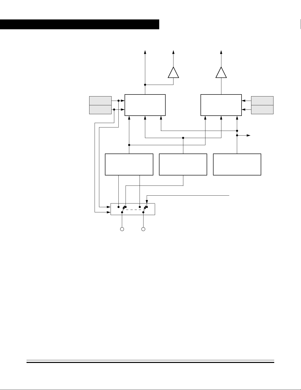
Oscillator (OSC)
Freescale Semiconductor, Inc.
nc...
I
cale Semiconductor,
Frees
7.2 Clock Selection
To CGM and others
CGMXCLK CGMRCLK
MOR CONFIG2
OSCSEL1
MUX
OSCSEL0
XCLK
X-TAL OSCILLATOR RC OSCILLATOR INTERNAL OSCILLATOR
OSC1 OSC2
To CGM PLL
RCCLK
To TBM
MUX
XRCIXRCI
BUS CLOCK
OSCCLK
ICLK
From SIM
Figure 7-1. Oscillator Module Block Diagram
Reference clocks are selectable for the following sub-systems:
OSCCLK1
OSCCLK0
To SIM
(and COP)
• CGMXCLK and CGMRCLK — Reference clock for clock
generator module (CGM) and other MCU sub-systems other than
TBM and COP. This is the main reference clock for the MCU.
• OSCCLK — Reference clock for timebase module (TBM).
Data Sheet MC68HC908AP Family — Rev. 2.5
92 MOTOROLA
For More Information On This Product,
Go to: www.freescale.com
Freescale Semiconductor, Inc.
7.2.1 CGM Reference Clock Selection
The clock generator module (CGM) reference clock (CGMXCLK) is the
reference clock input to the MCU. It is selected by programming two bits
in a FLASH memory location; the mask option register (MOR), at
$FFCF. See 5.5 Mask Option Register (MOR).
Address: $FFCF
Bit 7654321Bit 0
Read:
OSCSEL1OSCSEL0RRRRRR
Write:
Oscillator (OSC)
Clock Selection
nc...
I
cale Semiconductor,
Frees
Reset: Unaffected by reset
Erased:11111111
R=Reserved
Figure 7-2. Mask Option Register (MOR)
Table 7-1. CGMXCLK Clock Selection
OSCSEL1 OSCSEL0 CGMXCLK OSC2 Pin Comments
0 0 — — Not used
01ICLKf
1 0 RCCLK f
11XCLK
BUS
BUS
Inverting
output of
X-TAL
Internal oscillator generates the CGMXCLK.
RC oscillator generates the CGMXCLK.
Internal oscillator is available after each POR
or reset.
X-tal oscillator generates the CGMXCLK.
Internal oscillator is available after each POR
or reset.
The internal oscillator is a free running oscillator and is available after
each POR or reset. It is turned-off in stop mode by setting the
STOP_ICLKDIS bit in CONFIG2.
MC68HC908AP Family — Rev. 2.5 Data Sheet
MOTOROLA 93
For More Information On This Product,
Go to: www.freescale.com
Freescale Semiconductor, Inc.
Oscillator (OSC)
7.2.2 TBM Reference Clock Selection
The timebase module reference clock (OSCCLK) is selected by
configuring two bits in the CONFIG2 register, at $001D. See 5.4
Configuration Register 2 (CONFIG2).
Address: $001D
Bit 7654321Bit 0
nc...
I
cale Semiconductor,
Frees
NOTE: The RCCLK or XCLK is only available if that clock is selected as the
7.3 Internal Oscillator
Read:
Write:
Reset:00000000
STOP_
ICLKDIS
STOP_
RCLKEN
STOP_
XCLKEN
OSCCLK1 OSCCLK0
00
SCIBDSRC
Figure 7-3. Configuration Register 2 (CONFIG2)
Table 7-2. Timebase Module Reference Clock Selection
OSCCLK1 OSCCLK0 Timebase Clock Source
0 0 Internal oscillator (ICLK)
0 1 RC oscillator (RCCLK)
1 0 X-tal oscillator (XCLK)
1 1 Not used
CGM reference clock, whereas the ICLK is always available.
The internal oscillator clock (ICLK), with a frequency of f
, is a free
ICLK
running clock that requires no external components. It can be selected
as the CGMXCLK for the CGM and MCU sub-systems; and the
OSCCLK clock for the TBM. The ICLK is also the reference clock input
to the computer operating properly (COP) module.
Due to the simplicity of the internal oscillator, it does not have the
accuracy and stability of the RC oscillator or the x-tal oscillator.
Therefore, the ICLK is not suitable where an accurate bus clock is
required and it should not be used as the CGMRCLK to the CGM PLL.
Data Sheet MC68HC908AP Family — Rev. 2.5
94 MOTOROLA
For More Information On This Product,
Go to: www.freescale.com
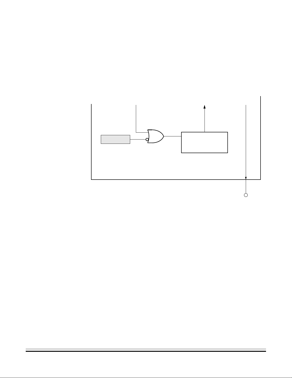
Freescale Semiconductor, Inc.
Oscillator (OSC)
RC Oscillator
The internal oscillator by default is always available and is free running
after POR or reset. It can be turned-off in stop mode by setting the
STOP_ICLKDIS bit before executing the STOP instruction.
Figure 7-4 shows the logical representation of components of the
internal oscillator circuitry.
From SIM
SIMOSCEN
nc...
I
CONFIG2
STOP_ICLKDIS
MCU
To Clock Selection MUX
and COP
ICLK
EN
INTERNAL OSCILLATOR
BUS CLOCK
Figure 7-4. Internal Oscillator
7.4 RC Oscillator
cale Semiconductor,
The RC oscillator circuit is designed for use with an external resistor and
a capacitor.
From SIM
OSC2
Frees
In its typical configuration, the RC oscillator requires two external
components, one R and one C. Component values should have a
tolerance of 1% or less, to obtain a clock source with less than 10%
tolerance. The oscillator configuration uses two components:
•C
EXT
•R
EXT
MC68HC908AP Family — Rev. 2.5 Data Sheet
MOTOROLA 95
For More Information On This Product,
Go to: www.freescale.com

Oscillator (OSC)
Freescale Semiconductor, Inc.
nc...
I
cale Semiconductor,
Frees
7.5 X-tal Oscillator
From SIM
SIMOSCEN
CONFIG2
STOP_RCLKEN
MCU
See Section 24. for component value requirements.
To Clock Selection MUX
RCCLK
EN
RC OSCILLATOR
OSC1
V
REG
R
EXT
From SIM
BUS CLOCK
OSC2
C
EXT
Figure 7-5. RC Oscillator
The crystal (x-tal) oscillator circuit is designed for use with an external
32.768kHz crystal to provide an accurate clock source.
In its typical configuration, the x-tal oscillator is connected in a Pierce
oscillator configuration, as shown in Figure 7-6. This figure shows only
the logical representation of the internal components and may not
represent actual circuitry. The oscillator configuration uses five
components:
• Crystal, X
• Fixed capacitor, C
(32.768kHz)
1
1
• Tuning capacitor, C2 (can also be a fixed capacitor)
• Feedback resistor, R
B
• Series resistor, RS (optional)
Data Sheet MC68HC908AP Family — Rev. 2.5
96 MOTOROLA
For More Information On This Product,
Go to: www.freescale.com

Freescale Semiconductor, Inc.
Oscillator (OSC)
I/O Signals
nc...
I
cale Semiconductor,
Frees
7.6 I/O Signals
From SIM
SIMOSCEN
CONFIG2
STOP_XCLKEN
MCU
See Section 24. for component value requirements.
C
To Clock Selection MUX
R
B
X
1
32.768kHz
1
XCLK
OSC2OSC1
R
S
C
2
Figure 7-6. Crystal Oscillator
The series resistor (R
) is included in the diagram to follow strict Pierce
S
oscillator guidelines and may not be required for all ranges of operation,
especially with high frequency crystals. Refer to the crystal
manufacturer’s data for more information.
The following paragraphs describe the oscillator I/O signals.
7.6.1 Crystal Amplifier Input Pin (OSC1)
OSC1 pin is an input to the crystal oscillator amplifier or the input to the
RC oscillator circuit.
MC68HC908AP Family — Rev. 2.5 Data Sheet
MOTOROLA 97
For More Information On This Product,
Go to: www.freescale.com

Freescale Semiconductor, Inc.
Oscillator (OSC)
7.6.2 Crystal Amplifier Output Pin (OSC2)
When the x-tal oscillator is selected, OSC2 pin is the output of the crystal
oscillator inverting amplifier.
When the RC oscillator or internal oscillator is selected, OSC2 pin is the
output of the internal bus clock.
7.6.3 Oscillator Enable Signal (SIMOSCEN)
The SIMOSCEN signal from the system integration module (SIM)
enables/disables the x-tal oscillator, the RC-oscillator, or the internal
nc...
I
oscillator circuit.
cale Semiconductor,
Frees
7.6.4 CGM Oscillator Clock (CGMXCLK)
The CGMXCLK clock is output from the x-tal oscillator, RC oscillator or
the internal oscillator. This clock drives to CGM and other MCU sub-
7.6.5 CGM Reference Clock (CGMRCLK)
7.6.6 Oscillator Clock to Time Base Module (OSCCLK)
systems.
This is buffered signal of CGMXCLK, it is used by the CGM as the
phase-locked-loop (PLL) reference clock.
The OSCCLK is the reference clock that drives the timebase module.
See Section 12. Timebase Module (TBM).
7.7 Low Power Modes
The WAIT and STOP instructions put the MCU in low-power
consumption standby modes.
Data Sheet MC68HC908AP Family — Rev. 2.5
98 MOTOROLA
For More Information On This Product,
Go to: www.freescale.com

Freescale Semiconductor, Inc.
7.7.1 Wait Mode
The WAIT instruction has no effect on the oscillator module. CGMXCLK
continues to drive to the clock generator module, and OSCCLK
continues to drive the timebase module.
7.7.2 Stop Mode
The STOP instruction disables the x-tal or the RC oscillator circuit, and
hence the CGMXCLK clock stops running. For continuous x-tal or RC
oscillator operation in stop mode, set the STOP_XCLKEN (for x-tal) or
nc...
I
STOP_RCLKEN (for RC) bit to logic 1 before entering stop mode.
The internal oscillator clock continues operation in stop mode. It can be
disabled by setting the STOP_ICLKDIS bit to logic 1 before entering stop
mode.
Oscillator (OSC)
Oscillator During Break Mode
cale Semiconductor,
Frees
7.8 Oscillator During Break Mode
The oscillator continues to drive CGMXCLK when the device enters the
break state.
MC68HC908AP Family — Rev. 2.5 Data Sheet
MOTOROLA 99
For More Information On This Product,
Go to: www.freescale.com

Freescale Semiconductor, Inc.
Oscillator (OSC)
nc...
I
cale Semiconductor,
Frees
Data Sheet MC68HC908AP Family — Rev. 2.5
100 MOTOROLA
For More Information On This Product,
Go to: www.freescale.com
 Loading...