


1995 Motorola, Inc. All Rights Reserved.
MC68HC901
Multi-Function Peripheral
User’s Manual
Motorola reserves the right to make changes without further notice to any products herein. Motorola mak es no warranty, representation or guarantee regarding
the suitability of its products for any particular purpose, nor does Motorola assume an y liability arising out of the application or use of any product or circuit, and
specifically disclaims any and all liability, including without limitation consequential or incidental damages. "Typical" parameters can and do vary in different
applications. All operating parameters, including "T ypicals" must be validated for each customer application by customer's technical experts. Motorola does not
convey any license under its patent rights nor the rights of others. Motorola products are not designed, intended, or authorized for use as components in
systems intended for surgical implant into the body , or other applications intended to support or sustain life, or f or any other application in which the failure of the
Motorola product could create a situation where personal injury or death may occur. Should Buyer purchase or use Motorola products for any such unintended
or unauthorized application, Buyer shall indemnify and hold Motorola and its officers, employees, subsidiaries, affiliates, and distributors harmless against all
claims, costs, damages, and expenses, and reasonable attorney fees arising out of, directly or indirectly, any claim of personal injury or death associated with
such unintended or unauthorized use, even if such claim alleges that Motorola was negligent regarding the design or manufacture of the part. Motorola and
are registered trademarks of Motorola, Inc. Motorola, Inc. is an Equal Opportunity/Affirmative Action Employer.

ii
MC68HC901 USER’S MANUAL
MOTOROLA
Trademarks:
Motorola and the Motorola symbol are registered trademark(s) of Motorola, Inc.

MOTOROLA
MC68HC901 USER’S MANUAL
iii
68K FAX-IT
Documentation Comments
FAX 512-891-8593—Documentation Comments Only
The Motorola High-Performance Embedded Systems Technical Communications
Department provides a fax number for you to submit any questions or comments about this
document or how to order other documents. We welcome your suggestions for improving
our documentation. Please do not fax technical questions.
Please provide the part number and revision number (located in upper right-hand corner of
the cover) and the title of the document. When referring to items in the manual, please
reference by the page number, paragraph number, figure number, table number, and line
number if needed.
When sending a fax, please provide your name, company, fax number, and phone number
including area code.
For Internet Access:
Telnet: pirs.aus.sps.mot.com (Login: pirs)
WWW: http: / / pirs.aus.sps.mot.com/aesop/hmpg.html
Query By Email: aesop_query@pirs.aus.sps.mot.com
(Type “HELP’’ in text body.)
For Dial-Up:
Phone: +1-512-891-3650
Phone (US or Canada): 1-800-843-3451
Connection Settings: N/8/1/F
Data Rate: < 14,400 bps
Terminal Emulation: VT100
Login: pirs
For AESOP Questions:
FAX: +1-512-891-8775
EMAIL: aesop_sysop@pirs.aus.sps.mot.com
For Hotline Questions:
FAX (US or Canada): 1-800-248-8567
EMAIL: aesop_support@pirs.aus.sps.mot.com

iv
MC68HC901 USER’S MANUAL
MOTOROLA
Applications and Technical Information
For questions or comments pertaining to technical information, questions, and applications,
please contact one of the following sales offices nearest you.
— Sales Offices —
Field Applications Engineering Available Through All Sales Offices
UNITED STATES
ALABAMA , Huntsville (205) 464-6800
ARIZONA , Tempe (602) 897-5056
CALIFORNIA , Agoura Hills (818) 706-1929
CALIFORNIA , Los Angeles (310) 417-8848
CALIFORNIA , Irvine (714) 753-7360
CALIFORNIA , Rosevllle (916) 922-7152
CALIFORNIA , San Diego (619) 541-2163
CALIFORNIA , Sunnyvale (408) 749-0510
COLORADO , Colorado Springs (719) 599-7497
COLORADO , Denver (303) 337-3434
CONNECTICUT , Wallingford (203) 949-4100
FLORIDA , Maitland (407) 628-2636
FLORIDA , Pompano Beach/
Fort Lauderdale (305) 486-9776
FLORIDA , Clearwater (813) 538-7750
GEORGlA , Atlanta (404) 729-7100
IDAHO , Boise (208) 323-9413
ILLINOIS , Chicago/Hoffman Estates (708) 490-9500
INDlANA , Fort Wayne (219) 436-5818
INDIANA , Indianapolis (317) 571-0400
INDIANA , Kokomo (317) 457-6634
IOWA , Cedar Rapids (319) 373-1328
KANSAS , Kansas City/Mission (913) 451-8555
MARYLAND , Columbia (410) 381-1570
MASSACHUSETTS , Marborough (508) 481-8100
MASSACHUSETTS , Woburn (617) 932-9700
MICHIGAN , Detroit (313) 347-6800
MINNESOTA , Minnetonka (612) 932-1500
MISSOURI , St. Louis (314) 275-7380
NEW JERSEY , Fairfield (201) 808-2400
NEW YORK , Fairport (716) 425-4000
NEW YORK , Hauppauge (516) 361-7000
NEW YORK , Poughkeepsie/Fishkill (914) 473-8102
NORTH CAROLINA , Raleigh (919) 870-4355
OHIO , Cleveland (216) 349-3100
OHIO , Columbus/Worthington (614) 431-8492
OHIO , Dayton (513) 495-6800
OKLAHOMA , Tulsa (800) 544-9496
OREGON , Portland (503) 641-3681
PENNSYLVANIA , Colmar (215) 997-1020
Philadelphia/Horsham (215) 957-4100
TENNESSEE , Knoxville (615) 584-4841
TEXAS , Austin (512) 873-2000
TEXAS , Houston (800) 343-2692
TEXAS , Plano (214) 516-5100
VIRGINIA , Richmond (804) 285-2100
WASHINGTON , Bellevue (206) 454-4160
Seattle Access (206) 622-9960
WISCONSIN , Milwaukee/Brookfield (414) 792-0122
CANADA
BRITISH COLUMBIA , Vancouver (604) 293-7605
ONTARIO , Toronto (416) 497-8181
ONTARIO , Ottawa (613) 226-3491
QUEBEC , Montreal (514) 731-6881
INTERNATIONAL
AUSTRALIA , Melbourne (61-3)887-0711
AUSTRALIA , Sydney (61(2)906-3855
BRAZIL , Sao Paulo 55(11)815-4200
CHINA , Beijing 86 505-2180
FINLAND , Helsinki 358-0-35161191
Car Phone 358(49)211501
FRANCE , Paris/Vanves 33(1)40 955 900
GERMANY , Langenhagen/ Hanover 49(511)789911
GERMANY , Munich 49 89 92103-0
GERMANY , Nuremberg 49 911 64-3044
GERMANY , Sindelfingen 49 7031 69 910
GERMANY , Wiesbaden 49 611 761921
HONG KONG , Kwai Fong 852-4808333
Tai Po 852-6668333
INDIA , Bangalore (91-812)627094
ISRAEL , Tel Aviv 972(3)753-8222
ITALY , Milan 39(2)82201
JAPAN , Aizu 81(241)272231
JAPAN , Atsugi 81(0462)23-0761
JAPAN , Kumagaya 81(0485)26-2600
JAPAN , Kyushu 81(092)771-4212
JAPAN , Mito 81(0292)26-2340
JAPAN , Nagoya 81(052)232-1621
JAPAN , Osaka 81(06)305-1801
JAPAN, Sendai 81(22)268-4333
JAPAN, Tachikawa 81(0425)23-6700
JAPAN, Tokyo 81(03)3440-3311
JAPAN , Yokohama 81(045)472-2751
KOREA , Pusan 82(51)4635-035
KOREA , Seoul 82(2)554-5188
MALAYSIA , Penang 60(4)374514
MEXICO , Mexico City 52(5)282-2864
MEXICO , Guadalajara 52(36)21-8977
Marketing 52(36)21-9023
Customer Service 52(36)669-9160
NETHERLANDS , Best (31)49988 612 11
PUERTO RICO , San Juan (809)793-2170
SINGAPORE
(65)2945438
SPAIN , Madrid 34(1)457-8204
or 34(1)457-8254
SWEDEN , Solna 46(8)734-8800
SWITZERLAND , Geneva 41(22)7991111
SWITZERLAND , Zurich 41(1)730 4074
TAlWAN , Taipei 886(2)717-7089
THAILAND , Bangkok (66-2)254-4910
UNITED KINGDOM , Aylesbury 44(296)395-252
FULL LINE REPRESENTATIVES
COLORADO , Grand Junction
Cheryl Lee Whltely (303) 243-9658
KANSAS , Wichita
Melinda Shores/Kelly Greiving (316) 838 0190
NEVADA , Reno
Galena Technology Group (702) 746 0642
NEW MEXICO , Albuquerque
S&S Technologies, lnc. (505) 298-7177
UTAH
, Salt Lake City
Utah Component Sales, Inc. (801) 561-5099
WASHINGTON
, Spokane
Doug Kenley (509) 924-2322
ARGENTINA
, Buenos Aires
Argonics, S.A. (541) 343-1787
HYBRID COMPONENTS RESELLERS
Elmo Semiconductor (818) 768-7400
Minco Technology Labs Inc. (512) 834-2022
Semi Dice Inc. (310) 594-4631

v
MC68HC901 USER’S MANUAL
MOTOROLA
PREFACE
The complete documentation package for the MC68HC901 consists of the MC68HC901UM/
AD and the
M68000 Family Programmer’s Reference Manual
, which contains the complete
instruction set for the M68000 Family.
The
MC68HC901 Multi-Function Peripheral User’s Manual
describes the programming,
capabilities, registers, and operation of the MC68HC901. This device is the HCMOS version
of the older MC68901 device and provides enhanced performance in several areas. The
MC68HC901 provides a full-function single-channel USART, an eight-source interrupt
controller, four 8-bit timers, and eight parallel I/O lines.
The organization of this manual is as follows:
Section 1 Introduction
Section 2 Signal Description
Section 3 Bus Operation
Section 4 Interrupt Structure
Section 5 General Purpose Input/Output Port
Section 6 Timers
Section 7 Universal Synchronous/Asynchronous Receiver-Transmitter
Section 8 Electrical Characteristics
Section 9 Mechanical Data and Ordering Information

PRELIMINARY
MOTOROLA
MC68HC901 USER’S MANUAL
vii
TABLE OF CONTENTS
Paragraph Page
Number Title Number
Section 1
Introduction
1.1 Key Features .............................................................................................1-2
1.2 Register Programming ...............................................................................1-2
Section 2
Signal Description
2.1 Power Supply (V
CC
and GND) .................................................................. 2-1
2.2 Clock (CLK) .............................................................................................. 2-2
2.3 Data Bus (D7–D0) .................................................................................... 2-2
2.4 Asynchronous Bus Control ....................................................................... 2-2
2.4.1 Chip Select (CS
) .................................................................................. 2-2
2.4.2 Data Strobe (DS
) ................................................................................. 2-2
2.4.3 Read/Write (R/W
) ................................................................................ 2-2
2.4.4 Data Transfer Acknowledge (DTACK
) ................................................. 2-2
2.5 Register Select Bus (RS1–RS5) ............................................................... 2-2
2.6 Reset (RESET
) ......................................................................................... 2-2
2.7 Interrupt Control ........................................................................................ 2-3
2.7.1 Interrupt Request (IRQ
) ....................................................................... 2-3
2.7.2 Interrupt Acknowledge (IACK
) ............................................................. 2-3
2.7.3 Interrupt Enable In (IEI
) ....................................................................... 2-3
2.7.4 Interrupt Enable Out (IEO
) ................................................................... 2-3
2.8 General Purpose I/O Interrupt Lines (I7–I0) ............................................. 2-3
2.9 Timer Control ............................................................................................ 2-4
2.9.1 Timer Inputs (TAI and TBI) .................................................................. 2-4
2.9.2 Timer Outputs (TAO, TBO, TCO, and TDO) ....................................... 2-4
2.9.3 Timer Clock (XTAL1 and XTAL2) ........................................................ 2-4
2.10 Serial I/O Control ...................................................................................... 2-4
2.10.1 Serial Input (SI) .................................................................................... 2-4
2.10.2 Serial Output (SO) ............................................................................... 2-5
2.10.3 Receiver Clock (RC) ............................................................................ 2-5
2.10.4 Transmitter Clock (TC) ........................................................................ 2-5
2.11 Direct Memory Access Control ................................................................. 2-5
2.11.1 Receiver Ready (RR
) .......................................................................... 2-5
2.11.2 Transmitter Ready (TR
) ....................................................................... 2-5
2.12 Signal Summary ....................................................................................... 2-5

TABLE OF CONTENTS (Continued)
Paragraph Page
Number Title Number
viii
MC68HC901 USER’S MANUAL
MOTOROLA
Section 3
Bus Operation
3.1 Data Transfer Operations ......................................................................... 3-1
3.1.1 Read Cycle .......................................................................................... 3-1
3.1.2 Write Cycle .......................................................................................... 3-2
3.2 Interrupt Acknowledge Operation ............................................................. 3-2
3.3 Reset Operation ....................................................................................... 3-3
Section 4
Interrupt Structure
4.1 Interrupt Processing ................................................................................. 4-1
4.1.1 Interrupt Channel Prioritization ............................................................ 4-1
4.1.2 Interrupt Vector Number ...................................................................... 4-1
4.1.3 Vector Register (VR) ........................................................................... 4-2
4.2 Daisy-Chaining MFPs ............................................................................... 4-3
4.3 Interrupt Control Registers ....................................................................... 4-4
4.3.1 Interrupt Enable Registers (IERA, IERB) ............................................ 4-4
4.3.2 Interrupt Pending Registers (IPRA, IPRB) .......................................... 4-6
4.3.3 Interrupt Mask Registers (IMRA, IMRB) .............................................. 4-8
4.3.4 Interrupt In-Service Registers (ISRA, ISRB) ..................................... 4-10
4.4 Nesting MFP Interrupts ........................................................................... 4-11
4.4.1 Selecting the End-Of-Interrupt Mode ................................................. 4-11
4.4.2 Automatic End-Of-Interrupt Mode ..................................................... 4-12
4.4.3 Software End-Of-Interrupt Mode ....................................................... 4-12
Section 5
General Purpose Input/Output Port
5.1 GPIP Control Registers ............................................................................ 5-1
5.1.1 General Purpose I/O Data Register (GPDR) ....................................... 5-1
5.1.2 Active Edge Register (AER) ................................................................ 5-1
5.1.3 Data Direction Register (DDR) ............................................................ 5-2
Section 6
Timers
6.1 Operation Modes ...................................................................................... 6-1
6.1.1 Delay Mode Operation ........................................................................ 6-1
6.1.2 Pulse Width Measurement Operation ................................................. 6-2
6.1.3 Event Count Mode Operation .............................................................. 6-3
6.2 Timer Registers ........................................................................................ 6-4

TABLE OF CONTENTS (Continued)
Paragraph Page
Number Title Number
MOTOROLA
MC68HC901 USER’S MANUAL
ix
6.2.1 Timer Data Registers (TxDR) .............................................................. 6-4
6.2.2 Timer Control Registers (TxCR) .......................................................... 6-4
Section 7
Universal Synchronous/Asynchronous Receiver-Transmitter
7.1 Character Protocols .................................................................................. 7-1
7.1.1 Asynchronous Format ......................................................................... 7-2
7.1.2 Synchronous Format ........................................................................... 7-2
7.1.3 USART Control Register (UCR) .......................................................... 7-3
7.1.4 USART Data Register (UDR) .............................................................. 7-4
7.2 Receiver .................................................................................................... 7-4
7.2.1 Receiver Interrupt Channels ................................................................ 7-5
7.2.2 Receiver Status Register (RSR) .......................................................... 7-5
7.2.3 Special Receive Conditions ................................................................. 7-7
7.3 Transmitter ................................................................................................ 7-7
7.3.1 Transmitter Interrupt Channels ............................................................ 7-8
7.3.2 Transmitter Status Register (TSR) ...................................................... 7-8
7.4 DMA Operation ......................................................................................... 7-9
Section 8
Electrical Characteristics
8.1 Maximum Ratings ..................................................................................... 8-1
8.2 Thermal Characteristics ............................................................................ 8-1
8.3 Power Considerations ............................................................................... 8-2
8.4 DC Electrical Characteristics .................................................................... 8-3
8.5 Capacitance .............................................................................................. 8-3
8.6 Clock Timing ............................................................................................. 8-4
8.7 AC Electrical Characteristics .................................................................... 8-5
8.8 Timer AC Characteristics .......................................................................... 8-7
Section 9
Mechanical Data and Ordering Information
9.1 Pin Assignments ....................................................................................... 9-1
9.2 Package Dimensions ................................................................................ 9-2
9.3 Ordering Information ................................................................................. 9-4

PRELIMINARY
MOTOROLA
MC68HC901 USER’S MANUAL
xi
LIST OF ILLUSTRATIONS
Figure Page
Number Title Number
1-1. MFP Block Diagram ........................................................................................ 1-1
2-1. Input and Output Signals ................................................................................ 2-1
3-1. Read Cycle Timing Diagram ........................................................................... 3-2
3-2. Write Cycle Timing Diagram ........................................................................... 3-2
3-3. IACK
Cycle Timing Diagram ........................................................................... 3-3
4-1. Daisy-Chained Interrupt Structure ................................................................... 4-3
4-2. Conceptual Circuits of an Interrupt Channel ................................................... 4-9
6-1. Conceptual Circuit of Interrupt Source Selection ............................................ 6-2
8-1. Clock Input Timing Diagram ............................................................................ 8-4
8-2. MFP External Oscillator Components ............................................................. 8-4
8-3. Read Cycle Timing .......................................................................................... 8-8
8-4. Write Cycle Timing .......................................................................................... 8-8
8-5. Interrupt Acknowledge Cycle (IEI
Low) ........................................................... 8-9
8-6. Interrupt Acknowledge Cycle (IEI
High) ........................................................ 8-10
8-7. Interrupt Timing ............................................................................................. 8-10
8-8. Port Timing .................................................................................................... 8-10
8-9. Reset Timing ................................................................................................. 8-11
8-10. Receiver Timing ............................................................................................ 8-11
8-11. Transmitter Timing ........................................................................................ 8-11
8-12. Timer Timing ................................................................................................. 8-12
9-1. 48-Pin Dual-In-Line Package (Plastic) ............................................................ 9-1
9-2. 52-Lead QUAD Package ................................................................................. 9-2
9-3. Case 767-02–P Suffix ..................................................................................... 9-2
9-4. Case 778-02–FN Suffix ................................................................................... 9-3

PRELIMINARY
MOTOROLA
MC68HC901 USER’S MANUAL
xiii
LIST OF TABLES
Table Page
Number Title Number
1-1. MFP Register Map ......................................................................................... 1-2
2-1. Signal Summary ............................................................................................. 2-5
MOTOROLA
MC68HC901 USER’S MANUAL
1-1
SECTION 1
INTRODUCTION
The MC68HC901 Multi-Function Peripheral (MFP) is a member of the M68000 Family
of peripherals. Unless otherwise specified, the MC68HC901 multi-function peripheral
is hereafter referred to as the MFP in this document. Many features of the MFP make
reference to the MC68000 Family of 16- and 32-bit microprocessors, which includes the
MC68HC000, MC68HC001, and the MC68EC000. These microprocessors are referred
to as the MC68000 within this document.
The MFP directly interfaces to the MC68000 via the asynchronous bus structure. Both
vectored and polled interrupt schemes are supported with the MFP providing unique vector
number generation for each of its 16 interrupt sources. Additionally, handshake lines are
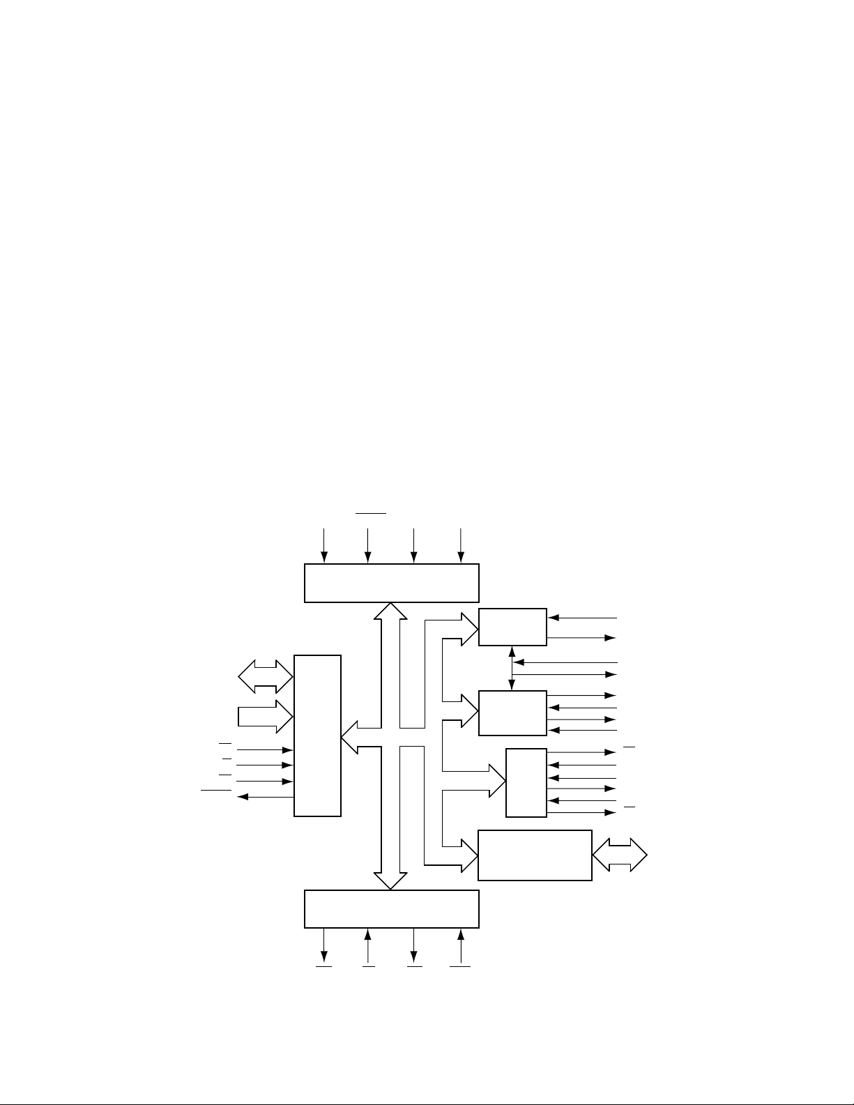
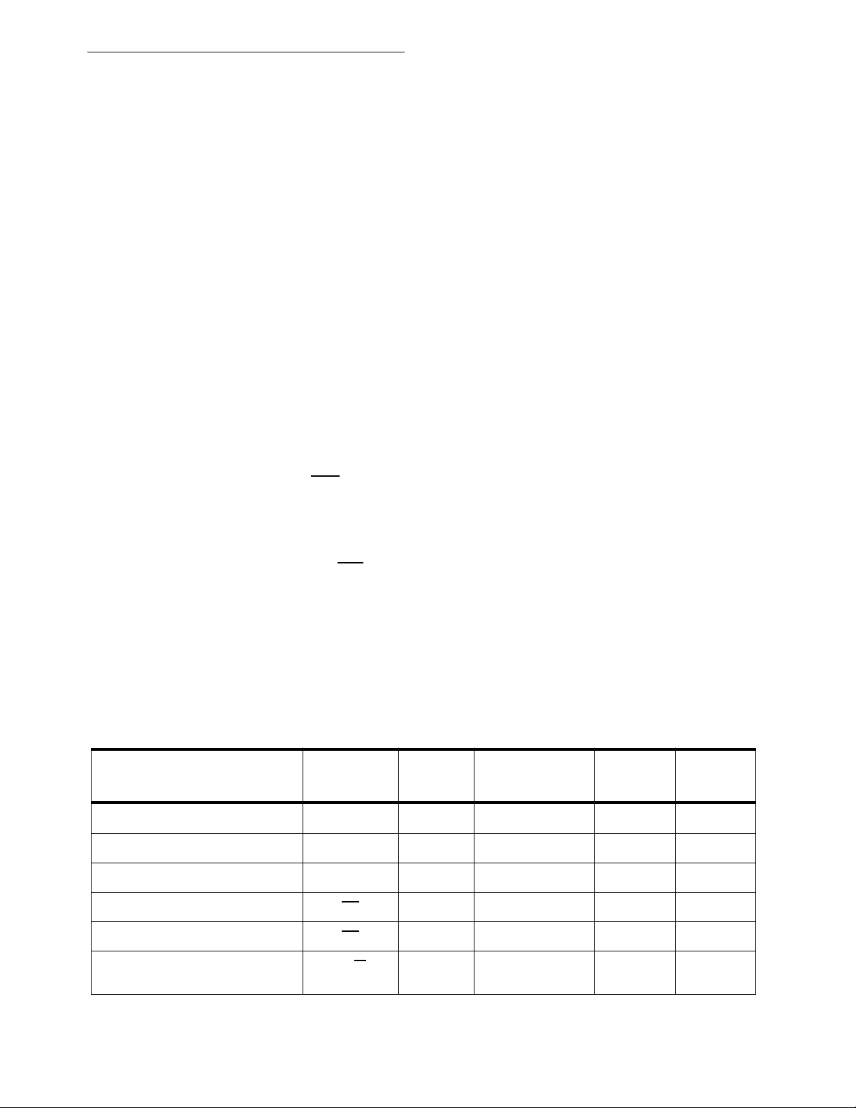
provided to facilitate direct memory access controller (DMAC) interfacing. Refer to Figure
1-1 for a block diagram of the MFP.
Figure 1-1. MFP Block Diagram
INTERNAL CONTROL
LOGIC
CLK GNDV
CC
RESET
TIMERS
C & D
TCO
TDO
XTAL1
XTAL2
TAO
TAI
TBO
TBI
TIMERS
A & B
USART
SI
RC
SO
TC
TR
RR
I / O INTERRUPTS
GENERAL PURPOSE
I0 – I7
CPU
BUS
I / O
INTERRUPT
CONTROL
IRQ
IEI IACK
D0 – D7
RS1 – RS5
R / W
DTACK
CS
DS
IEO
Introduction
1-2
MC68HC901 USER’S MANUAL
MOTOROLA
1.1 KEY FEATURES
The MFP performs many of the functions common to most microprocessor-based systems.
The resources available to the user include:
• Eight individually programmable I/O pins with interrupt capability
• 16-source interrupt controller with individual source enable and masking
• Four timers, two of which are multi-mode timers
• Single-channel full-duplex universal synchronous/asynchronous receiver-transmitter
(USART) which supports:
— asynchronous formats
— byte synchronous formats, with the addition of a polynomial generator checker
By incorporating multiple functions within the MFP, the system designer retains flexibility
while minimizing device count.
1.2 REGISTER PROGRAMMING
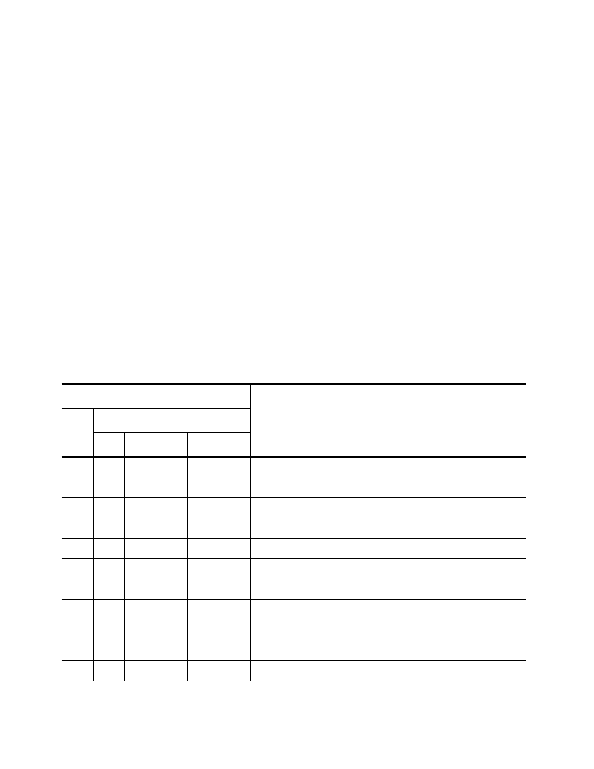
From a programmer's point of view, the versatility of the MFP may be attributed to its register
set. The registers are well organized and allow the MFP to be easily tailored to a variety
of applications. All of the 24 registers are also directly addressable which simplifies
programming. The register map is shown in Table 1-1.
Table 1-1. MFP Register Map
ADDRESS
ABBREVIATION REGISTER NAMEHEX BINARY
RS5 RS4 RS3 RS2 RS1
01 0 0 0 0 0 GPDR General Purpose I / O Data Register
03 0 0 0 0 1 AER Active Edge Register
05 0 0 0 1 0 DDR Data Direction Register
07 0 0 0 1 1 IERA Interrupt Enable Register A
09 0 0 1 0 0 IERB Interrupt Enable Register B
0B 0 0 1 0 1 IPRA Interrupt Pending Register A
0D 0 0 1 1 0 IPRB Interrupt Pending Register B
0F 0 0 1 1 1 ISRA Interrupt In-service Register A
11 0 1 0 0 0 ISRB Interrupt In-service Register B
13 0 1 0 0 1 IMRA Interrupt Mask Register A
15 0 1 0 1 0 IMRB Interrupt Mask Register B
Introduction
MOTOROLA
MC68HC901 USER’S MANUAL
1-3
17 0 1 0 1 1 VR Vector Register
19 0 1 1 0 0 TACR Timer A Control Register
1B 0 1 1 0 1 TBCR Timer B Control Register
1D 0 1 1 1 0 TCDCR Timers C and D Control Register
1F 0 1 1 1 1 TADR Timer A Data Register
21 1 0 0 0 0 TBDR Timer B Data Register
23 1 0 0 0 1 TCDR Timer C Data Register
25 1 0 0 1 0 TDCR Timer D Data Register
27 1 0 0 1 1 SCR Synchronous Character Register
29 1 0 1 0 0 UCR USART Control Register
2B 1 0 1 0 1 RSR Receiver Status Register
2D 1 0 1 1 0 TSR Transmitter Status Register
2F 1 0 1 1 1 UDR USART Data Register
NOTE: Hex addresses assume that RS1 connects with A1, RS2 connects with A2, etc., and that DS
is connected to
LDS
on the MC68000 or DS is connected to DS on the MC68008.
Table 1-1. MFP Register Map (Continued)
ADDRESS
ABBREVIATION REGISTER NAMEHEX BINARY
RS5 RS4 RS3 RS2 RS1
MOTOROLA
MC68HC901 USER’S MANUAL
2-1
SECTION 2
SIGNAL DESCRIPTION
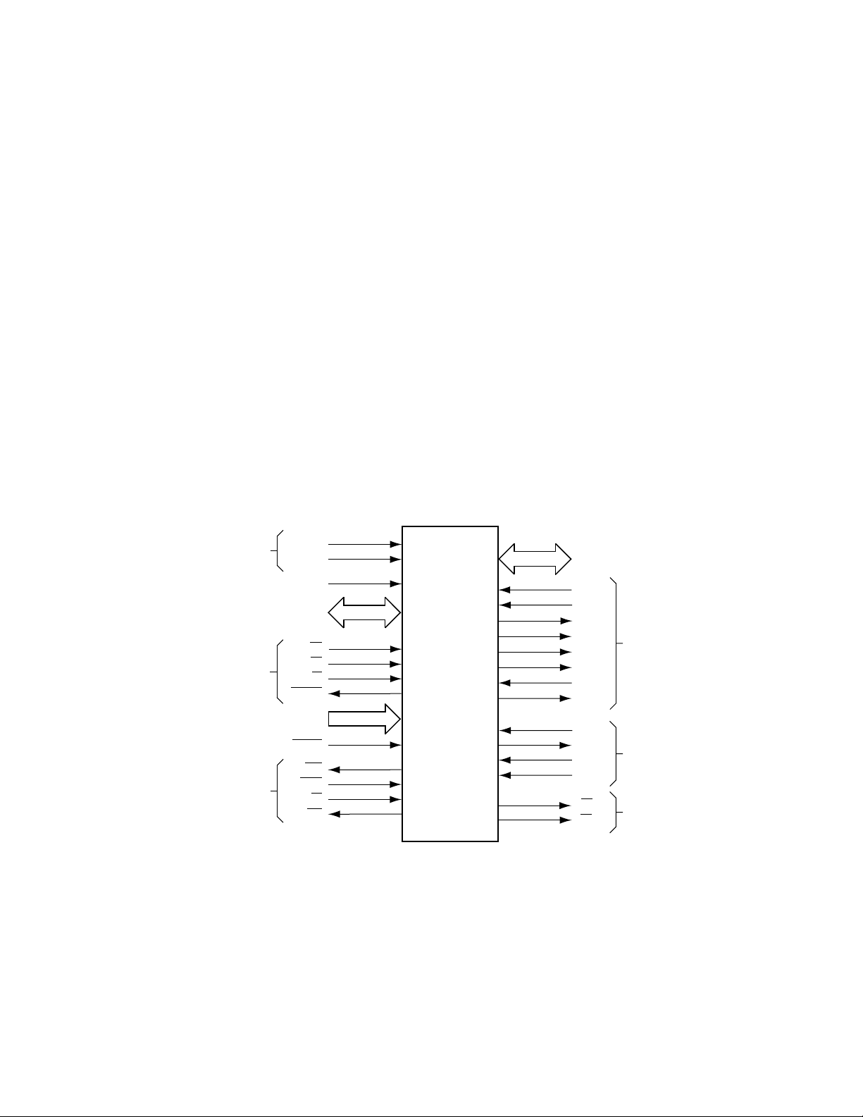
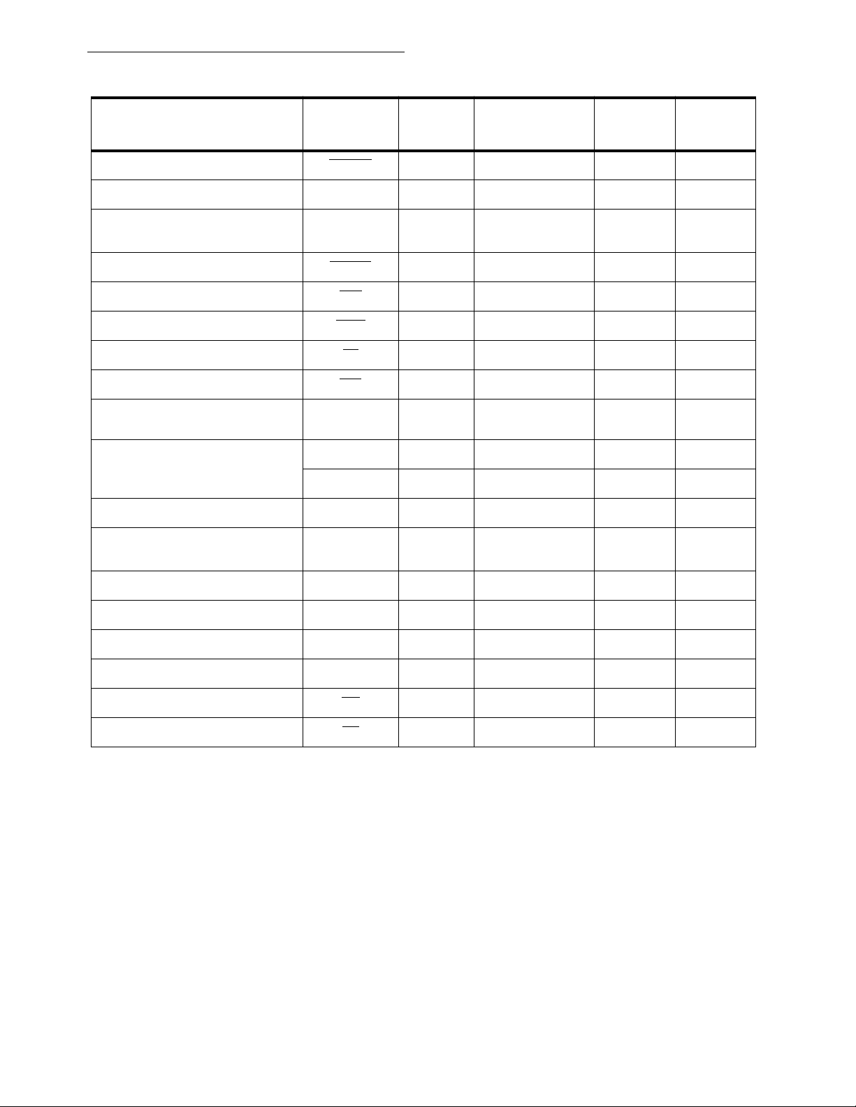
This section contains descriptions of the input and output signals. The input and output
signals can be functionally organized into groups as shown in Figure 2-1. The following
paragraphs provide a brief description of the signal and a reference (if applicable) to other
sections that contain more detail about its function.
NOTE
Assertion
and
negation
are used to specify forcing a signal to a
particular state.
Assertion
and
assert
refer to a signal that is
active or true.
Negation
and
negate
refer to a signal that is
inactive or false. These terms are used independently of the
voltage level (high or low) that they represent.
Figure 2-1. Input and Output Signals
2.1 POWER SUPPLY (V
CC
and GND)
Power is supplied to the MFP using these connections. The V
CC
pin is powered at +5 volts,
and ground is connected to the GND pins.
I0 – I7
TAI
TBI
TBO
TCO
TDO
XTAL1
XTAL2
SERIAL I / O
CONTROL
SI
SO
RC
TC
TAO
TIMER
CONTROL
TR
DATA BUS
D0 – D7
RS1 – RS5
IRQ
GND
CLK
V
CC
CS
DS
R / W
DTACK
INTERRUPT
CONTROL
ASYNCHRONOUS
BUS CONTROL
IEO
IEI
IACK
RESET
MC68HC901
MULTI-FUNCTION
PERIPHERAL
(MFP)
RR
REG SEL
POWER SUPPLY
GPIP
CONTROL
DMA

Signal Description
2-2
MC68HC901 USER’S MANUAL
MOTOROLA
2.2 CLOCK (CLK)
The clock input is a single-phase TTL-compatible signal used for internal timing. This input
must conform to minimum pulse width times. The clock is not necessarily the system clock
in frequency or phase.
2.3 DATA BUS (D7–D0)
This three-state bidirectional bus is used to transmit data to or receive data from the MFP
internal registers during a processor read or write cycle, respectively. During an interrupt
acknowledge cycle, the data bus is used to pass a vector number to the processor. The MFP
must be located on data bus lines D7–D0 when used with either the MC68000 series of
microprocessors and on data lines D31–D24 when used with the MC68020 microprocessor,
if vectored interrupts are to be used.
2.4 ASYNCHRONOUS BUS CONTROL
Asynchronous data transfers are controlled by chip select, data strobe, read/write, and data
transfer acknowledge. The register select lines, RS5–RS1, select an internal MFP register
for a read or write operation. The reset line initializes the MFP registers and the internal
control signals.
2.4.1 Chip Select (CS
)
This active low input activates the MFP for internal register access. CS
and IACK must not
be asserted at the same time.
2.4.2 Data Strobe (DS
)
This active low input is part of the internal chip select and interrupt acknowledge functions.
2.4.3 Read/Write (R/W
)
This input defines the current bus cycle as a read (high) or a write (low) cycle.
2.4.4 Data Transfer Acknowledge (DTACK
)
This active low, three-state output signals the completion of the operation phase of a bus
cycle to the processor. If the bus cycle is a process read, the MFP asserts DTACK to indicate
that the information on the data bus is valid. If the bus cycle is a processor write to the MFP,
DTACK
acknowledges the acceptance of the data by the MFP. DTACK will be asserted only
by a MFP that has CS
or IACK (and IEI) asserted.
2.5 REGISTER SELECT BUS (RS1–RS5)
The register select bus selects an internal MFP register during a read or write operation.
2.6 RESET (RESET
)
This active low input will initialize the MFP during powerup or in response to a total system
reset. Refer to Section 3.3 Reset Operation for further information.

Signal Description
MOTOROLA
MC68HC901 USER’S MANUAL
2-3
2.7 INTERRUPT CONTROL
The interrupt request and interrupt acknowledge signals are handshake lines for a vectored
interrupt scheme. Interrupt enable in and interrupt enable out implement a daisy-chained
interrupt structure.
2.7.1 Interrupt Request (IRQ
)
This active low, open-drain output signals to the processor that an interrupt is pending from
the MFP. There are 16 interrupt channels that can generate an interrupt request. Clearing
the interrupt pending registers (IPRA and IPRB) or clearing the interrupt mask registers
(IMRA and IMRB) will cause the IRQ
to be negated. IRQ will also be negated as the result
of an interrupt acknowledge cycle, unless additional interrupts are pending in the MFP.
Refer to Section 4 Interrupt Structure for further information.
2.7.2 Interrupt Acknowledge (IACK
)
If both IRQ
and IEI are asserted, the MFP will begin an interrupt acknowledge cycle when
IACK
and DS are asserted. The MFP will supply a unique vector number to the processor
which corresponds to the particular channel requesting interrupt service. In a daisy-chained
interrupt structure, all devices in the chain must have a common IACK
. Refer to Section 3.2
Interrupt Acknowledge Operation and Section 4.1.2 Interrupt Vector Number for
additional information. CS
and IACK must not be asserted at the same time.
2.7.3 Interrupt Enable In (IEI
)
This active low input, together with the IEO signal, provides a daisy-chained interrupt
structure for a vectored interrupt scheme. IEI
indicates that no higher priority device is
requesting interrupt service. So, the highest priority MFP in the chain should have its IEI
pin
tied low. During an interrupt acknowledge cycle, a MFP with a pending interrupt is not
allowed to pass a vector number to the processor until its IEI
pin is asserted. When the
daisy-chain option is not implemented, all MFPs should have their IEI
pin tied low. Refer to
Section 4.2 Daisy-Chaining MFPs for additional information.
2.7.4 Interrupt Enable Out (IEO
)
This active low output, together with the IEI signal, provides a daisy-chained interrupt
structure for a vectored interrupt scheme. The IEO
of a particular MFP signals lower priority
devices that neither it nor any other higher priority device is requesting interrupt service.
When a daisy-chain is implemented, IEO
is tied to the next lower priority MFP IEI input. The
lowest priority MFP is not connected. When the daisy-chain option is not implemented, IEO
is not connected. Refer to Section 4.2 Daisy-Chaining MFPs for additional information.
2.8 GENERAL PURPOSE I/O INTERRUPT LINES (I7–I0)
These lines constitute an 8-bit pin-programmable I/O port with interrupt capability. The data
direction register (DDR) individually defines each line as either a high-impedance input or a
TTL-compatible output. As an input, each line can generate an interrupt on the user selected
transition of the input signal. Refer to Section 5 General Purpose Input/Output Port for
further information.

Signal Description
2-4
MC68HC901 USER’S MANUAL
MOTOROLA
2.9 TIMER CONTROL
These lines provide internal timing and auxiliary timer control inputs required for certain
operating modes. Additionally, the timer outputs are included in this group.
2.9.1 Timer Inputs (TAI and TBI)
These input lines are control signals for timers A and B in the pulse width measurement
mode and the event count mode. These signals generate interrupts at the same priority level
as the general purpose I/O interrupt lines I4 and I3, respectively, when in the pulse width
measurement mode. While I4 and I3 do not have interrupt capability when timers A and B
are operated in this mode, they may still be used for I/O. Refer to Section 6.1.2 Pulse Width
Measurement Mode Operation and Section 6.1.3 Event Count Mode Operation for
further information.
2.9.2 Timer Outputs (TAO, TBO, TCO, and TDO)
Each timer has an associated output which toggles when its main counter counts through
01 (hexadecimal) regardless of which operational mode is selected. When in the delay
mode, the timer output will be a square wave with a period equal to two timer cycles. This
output may be used to supply the universal synchronous/asynchronous receiver-transmitter
(USART) baud rate clocks.
2.9.3 Timer Clock (XTAL1 and XTAL2)
These pins provide the timing signal for the four timers. A crystal can be connected between
the timer clock pins, XTAL1 and XTAL2, or XTAL1 can be driven with a CMOS-level clock
while XTAL2 is not connected. The following crystal parameters are suggested:
1. Parallel resonance, fundamental mode AT-cut, HC6 or HC33 holder
2. Frequency tolerance measured with 18 picofarads load (0.1% accuracy) – drive level
10 microwatts
3. Shunt capacitance equals 7 picofarads
4. Series resistance:
2.0 < f < 2.7 MHz; Rs ≤ 300 ohms
2.8 < f < 4.0 MHz; Rs ≤ 150 ohms
2.10 SERIAL I/O CONTROL
The full duplex serial channel is implemented by a serial input line. The independent receive
and transmit sections may be clocked by separate timing signals on the receive clock input
and the transmitter clock input.
2.10.1 Serial Input (SI)
This input line is the USART receiver data input. This input is not used in the USART
loopback mode. Refer to Section 7.3.2 Transmitter Status Register for additional
information.
Signal Description
2-5
MC68HC901 USER’S MANUAL
MOTOROLA
2.10.2 Serial Output (SO)
This output line is the USART transmitter data output. This output is in a high-impedance
state after a device reset.
2.10.3 Receiver Clock (RC)
This input controls the serial bit rate of the receiver. The signal may be supplied by the timer
output lines or by an external TTL-level clock which meets the minimum and maximum cycle
times. This clock is not used in the USART loopback mode. Refer to Section 7.3.2
Transmitter Status Register for additional information.
2.10.4 Transmitter Clock (TC)
This input controls the serial bit rate of the transmitter. This signal may be supplied by the
timer output lines or by an external TTL-level clock which meets the minimum and maximum
cycle times.
2.11 DIRECT MEMORY ACCESS CONTROL
The USART section of the MFP supports direct memory access transfers through its
receiver ready and transmitter ready status lines.
2.11.1 Receiver Ready (RR
)
This active low output reflects the receiver buffer full status (bit 7 in the Receiver Status
Register) for DMA operations.
2.11.2 Transmitter Ready (TR
)
This active low output reflects the transmitter buffer empty (bit 7 in the Transmitter Status
Register) for DMA operations.
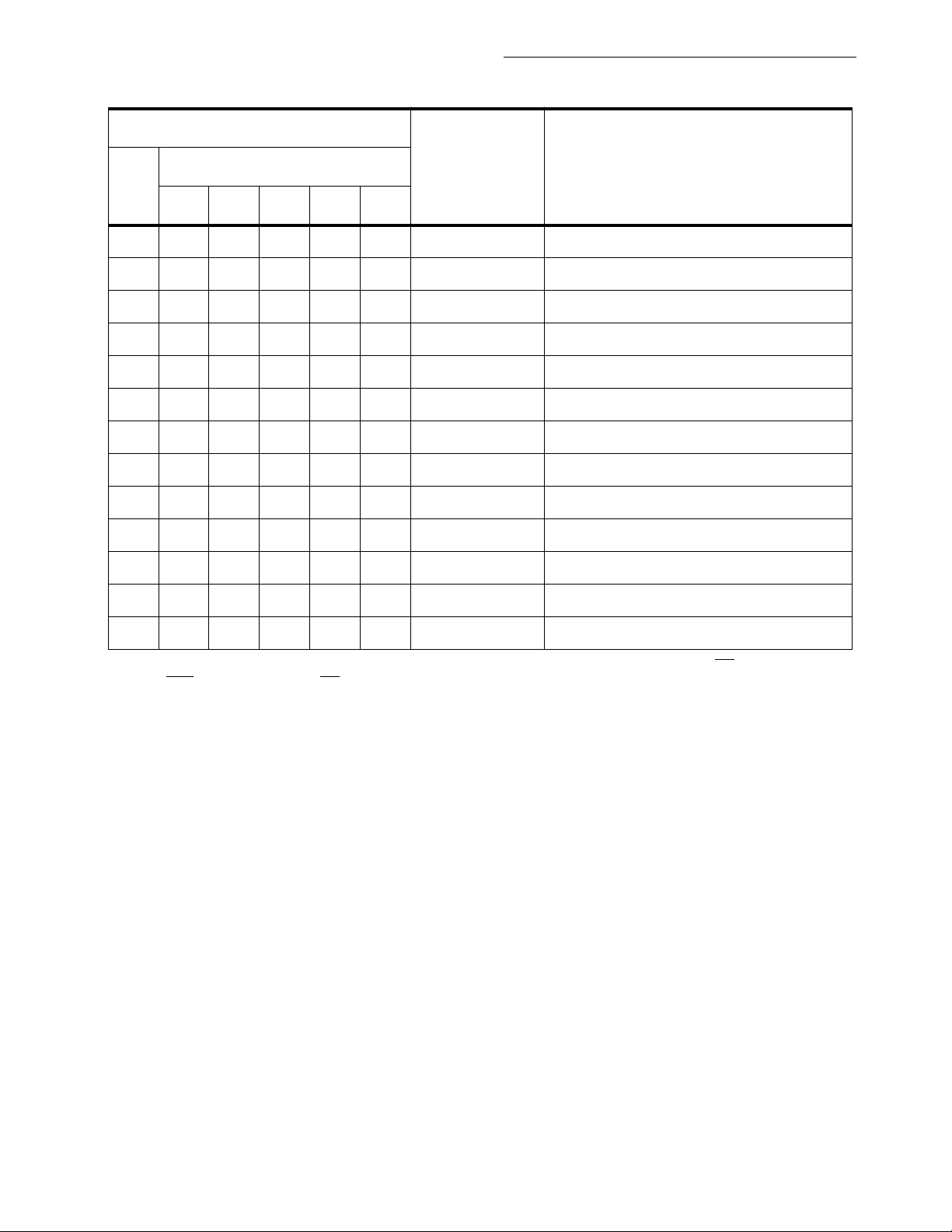
2.12 SIGNAL SUMMARY
The following table is a summary of all the signals discussed in the previous paragraphs.
Table 2-1. Signal Summary
SIGNAL NAME MNEMONIC
INPUT/
OUTPUT
ACTIVE
STATE
THREE-
STATE
RESET
STATE
Power Input V
CC
Input High — —
Ground GND Input Low — —
Clock CLK Input N / A
Chip Select CS
Input Low
Data Strobe DS
Input Low
Read / Write R / W
Input Read – High,
Write – Low
Signal Description
2-6
MC68HC901 USER’S MANUAL
MOTOROLA
Data Transfer Acknowledge DTACK
Output Low Yes High
Register Select Bus RS1 – RS5 Input N / A
Data Bus D0 – D7 Input /
Output
N / A Yes Hi-z
Reset RESET
Input Low
Interrupt Request IRQ
Output Low No* High
Interrupt Acknowledge IACK
Input Low
Interrupt Enable In IEI
Input Low
Interrupt Enable Out IEO
Output Low No High
General Purpose I / O I0 – I7 Input /
Output
N / A Yes Hi-Z
Timer Clock XTAL1 Input N / A
XTAL2 Output N / A No
Timer Inputs TAI, TBI Input N / A
Timer Outputs TAO, TBO,
TCO, TDO
Output N / A No Low
Serial Input SI Input N / A
Serial Output SO Output N / A Yes Hi-Z
Receiver Clock RC Input N / A
Transmitter Clock TC Input N / A
Receiver Ready RR
Output Low No High
Transmitter Ready TR
Output Low No Low
* Open Drain
Table 2-1. Signal Summary (Continued)
SIGNAL NAME MNEMONIC
INPUT/
OUTPUT
ACTIVE
STATE
THREE-
STATE
RESET
STATE

MOTOROLA
MC68HC901 USER’S MANUAL
3-1
SECTION 3
BUS OPERATION
The following paragraphs describe control signals and the bus operation during data
transfer, interrupt acknowledge, and reset operations.
3.1 DATA TRANSFER OPERATIONS
Transfer of data between devices involves the following pins:
• Register Select Bus – RS1 through RS5
• Data Bus – D0 through D7
• Control Signals
The address and data buses are separate parallel buses used to transfer data using an
asynchronous bus structure. In all cases, the bus master assumes responsibility for
deskewing all signals it issues at both the start and end of a cycle. Additionally, the bus
master is responsible for deskewing the acknowledge and data signals from the peripheral
devices.
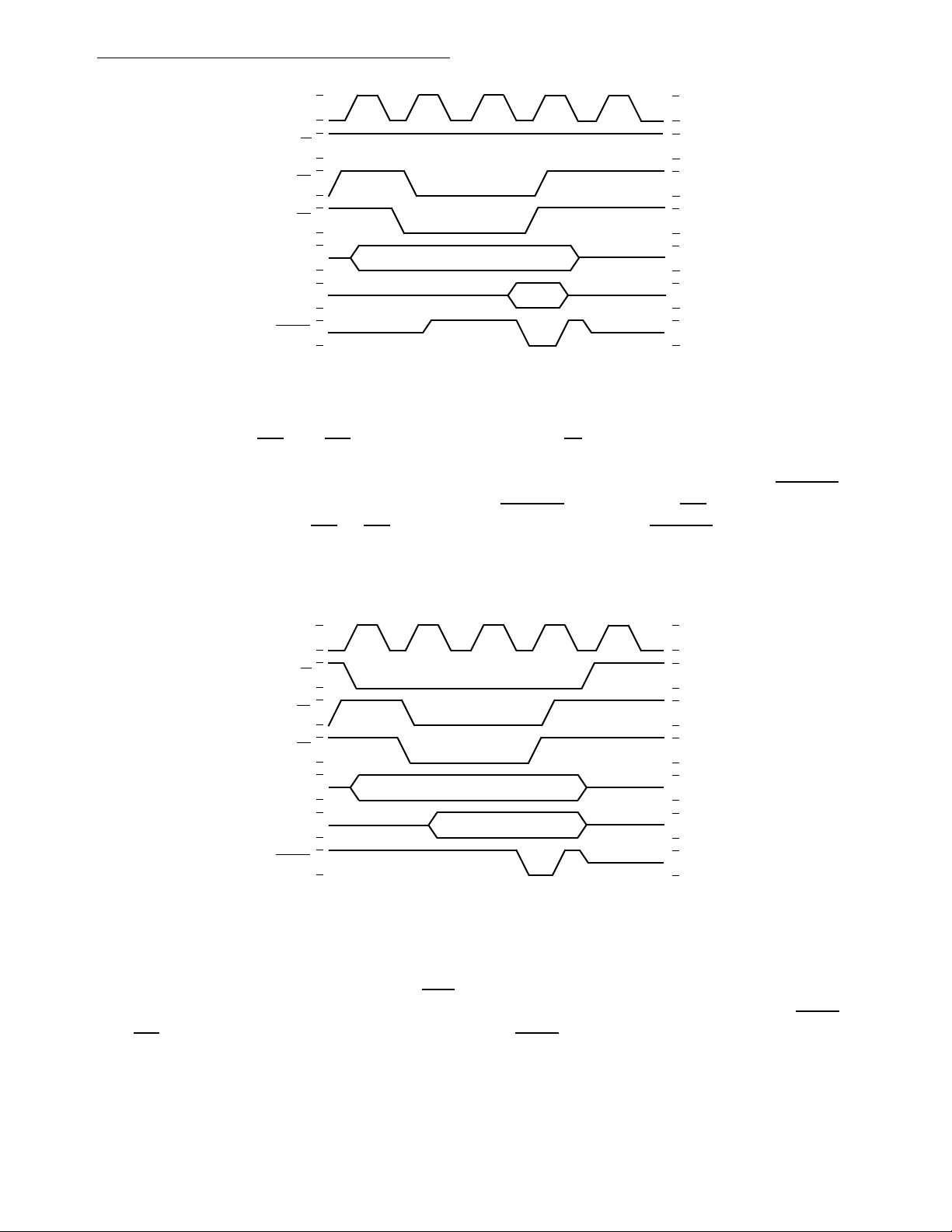
3.1.1 Read Cycle
To read an MFP register, CS
and DS must be asserted, and R/W must be high. The MFP
will place the contents of the register which is selected by the register select bus (RS1
through RS5) on the data bus (D0 through D7) and then assert DTACK
. The register
addresses are shown in Table 1-1.
After the processor has latched the data, it negates DS
. The negation of either CS or DS will
terminate the read operation. The MFP will drive DTACK
high and place it and the data bus
in the high-impedance state. The timing for a read cycle is shown in Figure 3-1. Refer to
Section 8.7 AC Electrical Characteristics for actual timing numbers.
Bus Operation
3-2
MC68HC901 USER’S MANUAL
MOTOROLA
Figure 3-1. Read Cycle Timing Diagram
3.1.2 Write Cycle
To write a register, CS
and DS must be asserted, and R/W must be low. The MFP will
decode the address bus to determine which register is selected. Then the register will be
loaded with the contents of the data bus on the next valid falling edge of CLK, and DTACK
will be asserted. When the processor recognizes DTACK
, it will negate DS. The write cycle
is terminated when either CS
or DS is negated. The MFP will drive DTACK high and place
it in the high-impedance state. The timing for a write cycle is shown in Figure 3-2. Refer to
Section 8.7 AC Electrical Characteristics for actual timing numbers.
Figure 3-2. Write Cycle Timing Diagram
3.2 INTERRUPT ACKNOWLEDGE OPERATION
The MFP has 16 interrupt sources: eight internal and eight external. When an interrupt
request is pending, the MFP will assert IRQ. In a vectored interrupt scheme, the processor
will acknowledge the interrupt request by performing an interrupt acknowledge cycle. IACK
and DS
will be asserted. The MFP responds to the IACK signal by placing a vector number
on the data bus. This vector number corresponds to the particular interrupt channel
requesting service. The format of this vector number is further discussed in Section 4.1.2
Interrupt Vector Number .
CLK
R / W
RS1 - RS5
D0 - D7
DTACK
CS
DS
CLK
R / W
RS1 - RS5
D0 - D7
DTACK
CS
DS

Bus Operation
MOTOROLA
MC68HC901 USER’S MANUAL
3-3
When the MFP asserts DTACK
to indicate that valid data is on the bus, the processor will
latch the data and terminate the bus cycle by negating DS
. When either DS or IACK is
negated, the MFP will terminate the interrupt acknowledge operation by driving DTACK
high
and placing it in the high-impedance state. IRQ
will be negated as a result of the IACK cycle
unless additional interrupts are pending.
The MFP can be part of a daisy-chain interrupt structure which allows multiple MFPs to be
placed at the same interrupt level by sharing a common IACK
signal. A daisy-chain priority
scheme is implemented with signals IEI
and IEO. IEI indicates that no higher priority device
is requesting interrupt service. IEO
signals lower priority devices that neither this device nor
any higher priority MFP is requesting service. To daisy-chain MFPs, the highest priority MFP
has its IEI
tied low and successive MFPs have their IEI connected to the next higher priority
MFPs IEO
. When the daisy-chain interrupt structure is not implemented, the IEIs of all MFPs
must be tied low and the IEO
s left unconnected. Refer to Section 4.2 Daisy-Chaining
MFPs for additional information.
When the processor initiates an interrupt acknowledge cycle by driving IACK
and DS, the
MFP, whose IEI
is low, may respond with a vector number if an interrupt is pending. If this
device does not have a pending interrupt, IEO
is asserted which allows the next lower
priority device to respond to the interrupt acknowledge. When an MFP propagates IEO
, it
will not drive the data bus nor DTACK
during the interrupt acknowledge cycle. The timing for
an IACK
cycle is shown in Figure 3-3. Refer to Section 8.7 AC Electrical Characteristics
and Figures 7-7 and 7-8 for further information.
Figure 3-3. IACK
Cycle Timing Diagram
3.3 RESET OPERATION
The reset operation will initialize the MFP to a known state. The reset operation requires that
the RESET
input be asserted for a minimum of two microseconds. During a device reset
condition, all internal MFP registers are cleared except for the timer data registers (TADR,
TBDR, TCDR, and TDDR), the USART data register (UDR), and the transmitter status
register (TSR). All timers are stopped, the USART receiver and transmitter are disabled, and
the serial output (SO) line is placed in high impedance. The interrupt channels are also
disabled and any pending interrupts are cleared. In addition, the general purpose interrupt
CLK
D0 - D7
DTACK
DS
IACK
IEI
IEO
 Loading...