

Motorola MC14LC5472FE, MC14LC5472FU, MC145472FE Datasheet
SEMICONDUCTOR TECHNICAL DATA
1
REV 1
Motorola, Inc. 1996
11/96
#*#!' '
%"&$%"' '
' #!%"' "$('& " ('$('&
'' #"")%' "
The MC74LCX16373 is a high performance, non–inverting 16–bit
transparent latch operating from a 2.7 to 3.6V supply. The device is byte
controlled. Each byte has separate Output Enable and Latch Enable
inputs. These control pins can be tied together for full 16–bit operation.
High impedance TTL compatible inputs significantly reduce current
loading to input drivers while TTL compatible outputs offer improved
switching noise performance. A VI specification of 5.5V allows
MC74LCX16373 inputs to be safely driven from 5V devices.
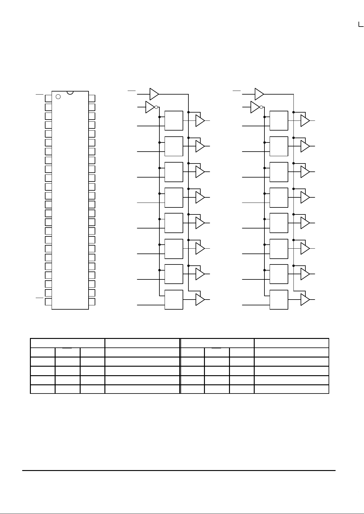
The MC74LCX16373 contains 16 D–type latches with 3–state
5V–tolerant outputs. When the Latch Enable (LEn) inputs are HIGH, data
on the Dn inputs enters the latches. In this condition, the latches are
transparent, i.e., a latch output will change state each time its D input
changes. When LE is LOW, the latches store the information that was
present on the D inputs a setup time preceding the HIGH–to–LOW
transition of LE. The 3–state outputs are controlled by the Output Enable
(OEn
) inputs. When OE is LOW, the outputs are enabled. When OE is
HIGH, the standard outputs are in the high impedance state, but this does
not interfere with new data entering into the latches.
• Designed for 2.7 to 3.6V V
CC
Operation
• 5.4ns Maximum t
pd
• 5V T olerant — Interface Capability With 5V TTL Logic
• Supports Live Insertion and Withdrawal
• I
OFF
Specification Guarantees High Impedance When VCC = 0V
• LVTTL Compatible
• LVCMOS Compatible
• 24mA Balanced Output Sink and Source Capability
• Near Zero Static Supply Current in All Three Logic States (20µA)
Substantially Reduces System Power Requirements
• Latchup Performance Exceeds 500mA
• ESD Performance: Human Body Model >2000V; Machine Model >200V
LOW–VOLTAGE
CMOS 16–BIT
TRANSPARENT LATCH
DT SUFFIX
PLASTIC TSSOP PACKAGE
CASE 1201–01
PIN NAMES
Function
Output Enable Inputs
Latch Enable Inputs
Inputs
Outputs
Pins
OEn
LEn
D0–D15
O0–O15
MC74LCX16373
MOTOROLA LCX DATA
BR1339 — REV 3
2
LOGIC DIAGRAM
481
LE1OE1
472
D0O0
463
D1O1
454
GNDGND
445
D2O2
436
D3O3
427
V
CC
V
CC
418
D4O4
409
D5O5
3910
GND
GND
3811
D6O6
3712
D7O7
3613
D8O8
3514
D9O9
3415
GNDGND
3316
D10O10
3217
D11O11
3118
V
CC
V
CC
3019
D12O12
2920
D13O13
2821
GNDGND
2722
D14O14
2623
D15
O15
2524
LE2OE2
O0
D0
O1
D1
O2
D2
O3
D3
O4
D4
O5
D5
O6
D6
O7
D7
nLE
Q
D
nLE
Q
D
nLE
Q
D
nLE
Q
D
nLE
Q
D
nLE
Q
D
nLE
Q
D
nLE
Q
D
LE1
OE1
O8
D8
O9
D9
O10
D10
O11
D11
O12
D12
O13
D13
O14
D14
O15
D15
nLE
Q
D
nLE
Q
D
nLE
Q
D
nLE
Q
D
nLE
Q
D
nLE
Q
D
nLE
Q
D
nLE
Q
D
LE2
OE2
1
48
24
25
2
47
3
46
5
44
6
43
8
41
9
40
11
38
12
37
13
36
14
35
16
33
17
32
19
30
20
29
22
27
23
26
Inputs Outputs Inputs Outputs
LE1 OE1 D0:7 O0:7 LE2 OE2 D8:15 O8:15
X H X Z X H X Z
H L L L H L L L
H L H H H L H H
L L X O0 L L X O0
H = High Voltage Level; L = Low V oltage Level; Z = High Impedance State; X = High or Low Voltage Level and T ransitions Are Acceptable, for I
CC
reasons, DO NOT FLOAT Inputs
 Loading...