

Motorola MC1489P, MC1489AP, MC1489D, MC1489AD Datasheet
T
75°C
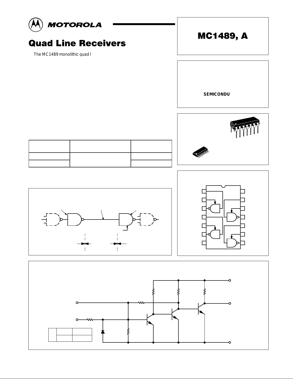
The MC1489 monolithic quad line receivers are designed to interface data
terminal equipment with data communications equipment in conformance
with the specifications of EIA Standard No. EIA–232D.
• Input Resistance – 3.0 k to 7.0 kΩ
• Input Signal Range – ± 30 V
• Input Threshold Hysteresis Built In
• Response Control
a) Logic Threshold Shifting
b) Input Noise Filtering
ORDERING INFORMATION
Operating
Device
MC1489P, AP
MC1489D, AD
Temperature Range
= 0 to +
A
°
Package
Plastic
SO–14
Order this document by MC1489/D
QUAD MDTL
LINE RECEIVERS
EIA–232D
SEMICONDUCTOR
TECHNICAL DATA
P SUFFIX
PLASTIC PACKAGE
CASE 646
D SUFFIX
PLASTIC PACKAGE
CASE 751A
(SO–14)
Line Driver
MC1488
MDTL Logic Input
Response Control 2
Simplified Application
Interconnecting
Cable
Interconnecting
Cable
Representative Schematic Diagram
Line Receiver
MC1489
MDTL Logic Output
(1/4 of Circuit Shown)
9.0 k
R
F
5.0 k
PIN CONNECTIONS
1
Input A
Response
2
Control A
3
Output A
4
Input B
Response
5
Control B
Output B
6
Ground
7
1.7 k
14
V
CC
3 Output
14
13
12
11
10
9
8
V
CC
Input D
Response
Control D
Output D
Input C
Response
Control C
Output C
Input 1
MC1489 MC1489A
RF6.7 kΩ 1.6 kΩ
MOTOROLA ANALOG IC DEVICE DATA
3.8 k
10 k
7 GND
Motorola, Inc. 1996 Rev 5
1
MC1489, A
MAXIMUM RATINGS (T
Power Supply Voltage V
Input Voltage Range V
Output Load Current I
= + 25°C, unless otherwise noted)
A
Rating
Symbol Value Unit
CC
IR
L
10 Vdc
± 30 Vdc
20 mA
Power Dissipation (Package Limitation, SO–14
and Plastic Dual In–Line Package)
Derate above TA = + 25°C
Operating Ambient Temperature Range T
Storage Temperature Range T
ELECTRICAL CHARACTERISTICS (Response control pin is open.) (V
P
D
1/
θJA
A
stg
1000
6.7
mW/°C
0 to + 75 °C
– 65 to + 175 °C
= + 5.0 Vdc ± 10%, TA = 0 to + 75°C, unless otherwise noted)
CC
Characteristics
Positive Input Current (VIH = + 25 Vdc)
(VIH = + 3.0 Vdc)
Negative Input Current (VIH = – 25 Vdc)
(VIH = – 3.0 Vdc)
Input Turn–On Threshold Voltage
(TA = + 25°C, VOL p 0.45 V)
MC1489
MC1489A
Input Turn–Off Threshold Voltage
(TA = + 25°C, VOH q 2.5 V, IL = – 0.5 mA) MC1489
MC1489A
Output Voltage High (VIH = 0.75 V, IL = – 0.5 mA)
(Input Open Circuit, IL = – 0.5 mA)
Output Voltage Low (VIL = 3.0 V, IL = 10 mA) V
Output Short–Circuit Current I
Power Supply Current (All Gates “on,” I
= 0 mA, VIH = + 5.0 Vdc) I
out
Power Consumption (VIH = + 5.0 Vdc) P
SWITCHING CHARACTERISTICS (V
Propagation Delay Time
= 5.0 Vdc ± 1%, TA = + 25°C, See Figure 1.)
CC
(RL = 3.9 kΩ) t
Rise Time (RL = 3.9 kΩ) t
Propagation Delay Time (RL = 390 kΩ) t
Fall Time (RL = 390 kΩ) t
mW
Symbol Min Typ Max Unit
I
I
V
V
V
OS
CC
PLH
TLH
PHL
THL
IH
IL
IH
IL
OH
OL
C
3.6
0.43
– 3.6
– 0.43
1.0
1.75
0.75
0.75
2.5
2.5
–
–
–
–
–
1.95
–
0.8
4.0
4.0
8.3
–
– 8.3
–
1.5
2.25
1.25
1.25
5.0
5.0
– 0.2 0.45 Vdc
– – 3.0 – 4.0 mA
– 16 26 mA
– 80 130 mW
– 25 85 ns
– 120 175 ns
– 25 50 ns
– 10 20 ns
mA
mA
Vdc
Vdc
Vdc
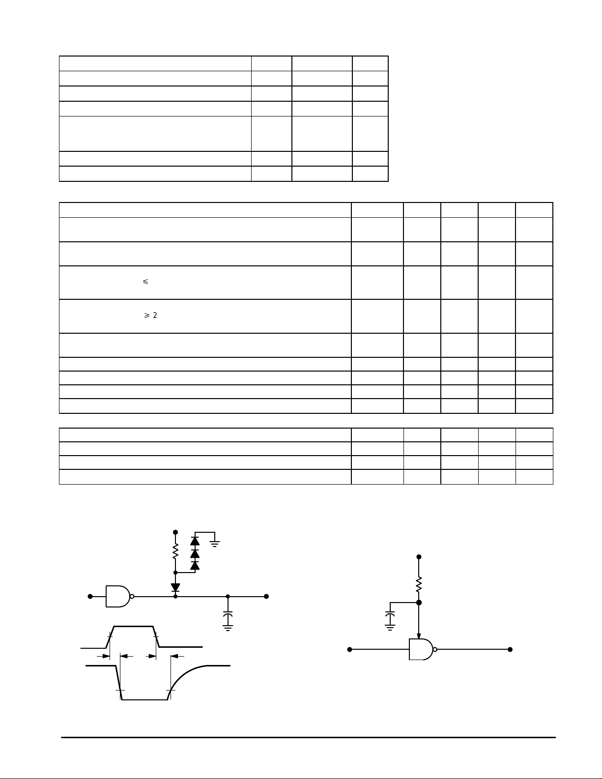
Figure 1. Switching Response
5.0 Vdc
R
L
E
in
3.0 V
E
in
E
O
50% 50%
t
PLH
t
t
THL
1.5 V
CL = 15 pF = total parasitic capacitance which includes
probe and wiring capacitances
TLH
1.5 V
2
All diodes
1N3064
or equivalent
C
L
t
TLH
TEST CIRCUITS
E
o
and t
THL
measured
10% – 90%
Figure 2. Response Control Node
C
1/4
V
in
MC1489A
C, capacitor is for noise filtering.
R, resistor is for threshold shifting.
MOTOROLA ANALOG IC DEVICE DATA
V
R
R
Response Node
V
O
 Loading...