

MOTOROLA MC1488M, MC1488MEL, MC1488ML1, MC1488DR2 Datasheet
SEMICONDUCTOR
TECHNICAL DATA
QUAD MDTL LINE DRIVER
EIA–232D
PIN CONNECTIONS
Order this document by MC1488/D
P SUFFIX
PLASTIC PACKAGE
CASE 646
D SUFFIX
PLASTIC PACKAGE
CASE 751A
(SO–14)
2
Output C
Input C2
Input C1
Output D
Input D2
V
CC
14
Input D1
V
EE
Input A
Output A
Input B1
Input B2
Gnd
Output B
8
9
10
11
12
13
7
5
3
4
1
6
1
MOTOROLA ANALOG IC DEVICE DATA
The MC1488 is a monolithic quad line driver designed to interface data
terminal equipment with data communications equipment in conformance
with the specifications of EIA Standard No. EIA–232D.
Features:
• Current Limited Output
±10 mA typical
• Power–Off Source Impedance
300 Ω mininum
• Simple Slew Rate Control with External Capacitor
• Flexible Operating Supply Range
• Compatible with All Motorola MDTL and MTTL Logic Families
ORDERING INFORMATION
Device
Operating
Temperature Range
Package
MC1488P
°
Plastic
MC1488D
T
A
=
0 to
+
75°C
SO–14
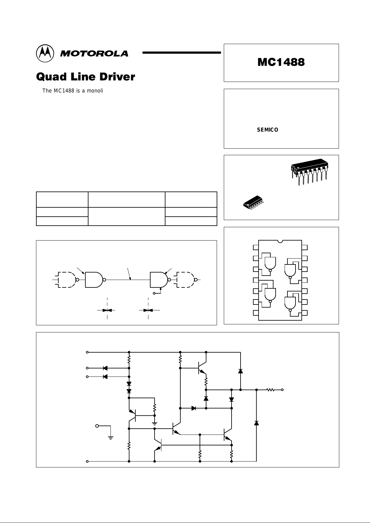
Circuit Schematic
(1/4 of Circuit Shown)
GND 7
3.6 k
Pins 4, 9, 12 or 2
Input
Pins 5, 10, 13
Input
8.2 k
VCC 14
7.0 k 70
6.2 k
70
Output
300
10 k
VEE 1
Pins 6, 8, 11 or 3
MDTL Logic Output
Interconnecting
Cable
Interconnecting
Cable
MDTL Logic Input
Line Receiver
MC1489
Simplified Application
Line Driver
MC1488
Motorola, Inc. 1996 Rev 3
MC1488
2
MOTOROLA ANALOG IC DEVICE DATA
MAXIMUM RATINGS (T
A
= +25°C, unless otherwise noted.)
Rating Symbol Value Unit
Power Supply Voltage V
CC
V
EE
+ 15
– 15
Vdc
Input Voltage Range V
IR
– 15 p VIR
p
7.0
Vdc
Output Signal Voltage V
O
±15 Vdc
Power Derating (Package Limitation, SO–14
and Plastic Dual–In–Line Package)
Derate above TA = + 25°C
P
D
1/R
θJA
1000
6.7
mW
mW/°C
Operating Ambient Temperature Range T
A
0 to + 75 °C
Storage Temperature Range T
stg
– 65 to + 175 °C
ELECTRICAL CHARACTERISTICS (V
CC
= + 9.0 ± 1% Vdc, VEE = –9.0 ± 1% Vdc, TA = 0 to 75°C, unless otherwise noted.)
Characteristic
Symbol Min Typ Max Unit
Input Current – Low Logic State (VIL = 0) I
IL
– 1.0 1.6 mA
Input Current – High Logic State (VIH = 5.0 V) I
IH
– – 10 µA
Output Voltage – High Logic State
(VIL = 0.8 Vdc, RL = 3.0 kΩ, VCC = + 9.0 Vdc, VEE = – 9.0 Vdc)
(VIL = 0.8 Vdc, RL = 3.0 kΩ, VCC = + 13.2 Vdc, VEE = – 13.2 Vdc)
V
OH
+ 6.0
+ 9.0
+7.0
+10.5
–
–
Vdc
Output Voltage – Low Logic State
(VIH = 1.9 Vdc, RL = 3.0 kΩ, VCC = + 9.0 Vdc, VEE = – 9.0 Vdc)
(VIH = 1.9 Vdc, RL = 3.0 kΩ, VCC = + 13.2 Vdc, VEE = – 13.2 Vdc)
V
OL
– 6.0
– 9.0
– 7.0
– 10.5
–
–
Vdc
Positive Output Short–Circuit Current, Note 1 I
OS+
+ 6.0 + 10 + 12 mA
Negative Output Short–Circuit Current, Note 1 I
OS–
– 6.0 – 10 – 12 mA
Output Resistance (VCC = VEE = 0, VO = ± 2.0 V) r
o
300 – – Ohms
Positive Supply Current (RI = ∞)
(VIH = 1.9 Vdc, VCC = + 9.0 Vdc)
(VIL = 0.8 Vdc, VCC = + 9.0 Vdc)
(VIH = 1.9 Vdc, VCC = + 12 Vdc)
(VIL = 0.8 Vdc, VCC = + 12 Vdc)
(VIH = 1.9 Vdc, VCC = + 15 Vdc)
(VIL = 0.8 Vdc, VCC = + 15 Vdc)
I
CC
–
–
–
–
–
–
+ 15
+ 4.5
+ 19
+ 5.5
–
–
+ 20
+ 6.0
+ 25
+ 7.0
+ 34
+ 12
mA
Negative Supply Current (RL = ∞)
(VIH = 1.9 Vdc, VEE = – 9.0 Vdc)
(VIL = 0.8 Vdc, VEE = – 9.0 Vdc)
(VIH = 1.9 Vdc, VEE = – 12 Vdc)
(VIL = 0.8 Vdc, VEE = – 12 Vdc)
(VIH = 1.9 Vdc, VEE = – 15 Vdc)
(VIL = 0.8 Vdc, VEE = – 15 Vdc)
I
EE
–
–
–
–
–
–
– 13
–
– 18
–
–
–
– 17
– 500
– 23
– 500
– 34
– 2.5
mA
µA
mA
µA
mA
mA
Power Consumption
(VCC = 9.0 Vdc, VEE = – 9.0 Vdc)
(VCC = 12 Vdc, VEE = – 12 Vdc)
P
C
–
–
–
–
333
576
mW
SWITCHING CHARACTERISTICS (V
CC
= +9.0 ± 1% Vdc, VEE = –9.0 ± 1% Vdc, TA = +25°C.)
Propagation Delay Time (zI = 3.0 k and 15 pF) t
PLH
– 275 350 ns
Fall Time (zI = 3.0 k and 15 pF) t
THL
– 45 75 ns
Propagation Delay Time (zI = 3.0 k and 15 pF) t
PHL
– 110 175 ns
Rise Time (zI = 3.0 k and 15 pF) t
TLH
– 55 100 ns
NOTE: 1. Maximum Package Power Dissipation may be exceeded if all outputs are shorted simultaneously.
MC1488
3
MOTOROLA ANALOG IC DEVICE DATA
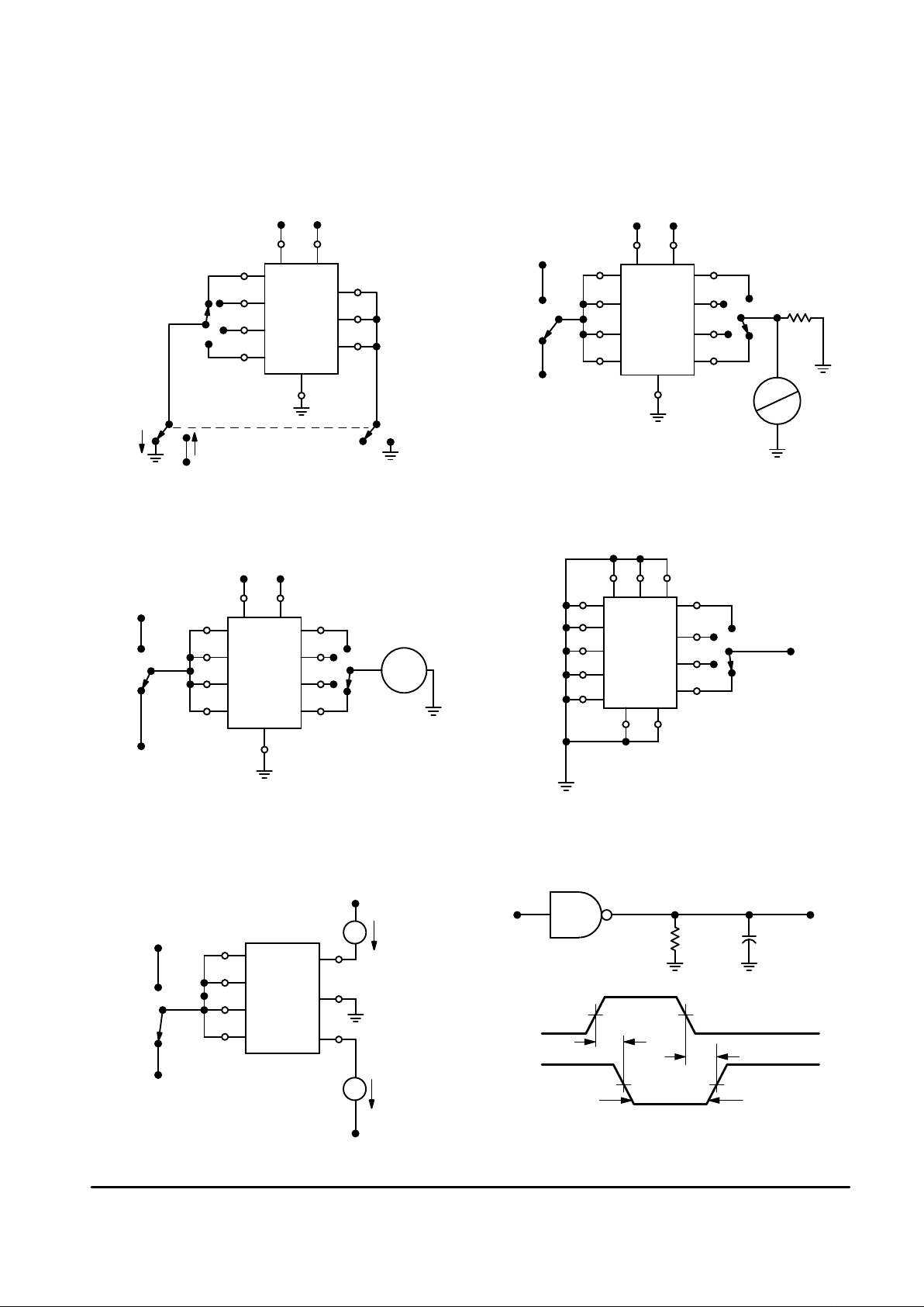
CHARACTERISTIC DEFINITIONS
Figure 1. Input Current Figure 2. Output Voltage
Figure 3. Output Short–Circuit Current Figure 4. Output Resistance (Power Off)
Figure 5. Power Supply Currents Figure 6. Switching Response
10
13
9
4
12
5
1
2
14
9.0 V
5.0 V
I
IH
I
IL
–9.0 V
7
1.9 V
7
V
OL
9.0 V
V
OH
0.8 V
V
OL
3.0 k
V
OH
14 1
–9.0 V
2
4
9
12
3
6
8
11
9
2
14
4
5
I
OS+
1
11
6
8
13
9
4
12
3
1
±
6.6 mA Max
3
7
8
6
11
0.8 V
2
1.9 V
14
V
EE
V
CC
7
10
12
I
OS
±
V
O
±
2.0 Vdc
I
OS–
t
THL
and t
TLH
Measured 10% to 90%
V
O
15 pF3.0 k
50%
t
PHL
t
PLH
t
TLH
t
THL
e
in
0 V
3.0 V
1.5 V
e
in
V
O
I
CC
V
IL
2
V
CC
1
14
7
12
4
9
I
EE
V
EE
1.9 V
V
IH
0.8 V
 Loading...