

Motorola MC145407P, MC145407DW Datasheet
MC145407MOTOROLA
1
Advance Information
EIA–232–E and CCITT V.28
The MC145407 is a silicon–gate CMOS IC that combines three drivers and
three receivers to fulfill the electrical specifications of EIA–232–E and CCITT
V.28 while operating from a single + 5 V power supply. A voltage doubler and
inverter convert the + 5 V to ± 10 V. This is accomplished through an on–board
20 kHz oscillator and four inexpensive external electrolytic capacitors. The
three drivers and three receivers of the MC145407 are virtually identical to
those of the MC145406. Therefore, for applications requiring more than three
drivers and/or three receivers, an M C145406 can be powered from an
MC145407, since the MC145407 charge pumps have been designed to
guarantee ± 5 V at the output of up to six drivers. Thus, the MC145407 provides
a high–performance, low–power, stand–alone solution or, with the MC145406,
a + 5 V only, high–performance two–chip solution.
Drivers
• ± 7.5 V Output Swing
• 300 Ω Power–Off Impedance
• Output Current Limiting
• TTL and CMOS Compatible Inputs
• Slew Rate Range Limited from 4 V/µs to 30 V/µs
Receivers
• + 25 V Input Range
• 3 to 7 kΩ Input Impedance
• 0.8 V Hysteresis for Enhanced Noise Immunity
Charge Pumps
• + 5 V to ± 10 V Dual Charge Pump Architecture
• Supply Outputs Capable of Driving Three On–Chip Drivers and Three
Drivers on the MC145406 Simultaneously
• Requires Four Inexpensive Electrolytic Capacitors
• On–Chip 20 kHz Oscillator
This document contains information on a new product. Specifications and information herein are subject to change without notice.
Order this document
by MC145407/D
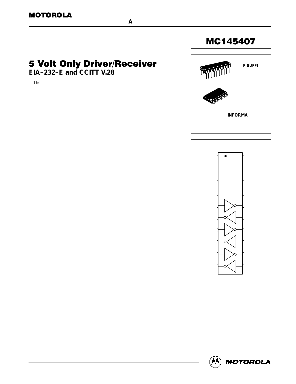
SEMICONDUCTOR TECHNICAL DATA
P SUFFIX
PLASTIC DIP
CASE 738
ORDERING INFORMATION
MC145407P Plastic DIP
MC145407DW SOG Package
DW SUFFIX
SOG PACKAGE
CASE 751D
20
1
20
1
R
R
D
R
D
D
C2+
GND
C2–
V
SS
Rx1
Tx1
Rx2
Tx2
Rx3
Tx3
C1+
V
CC
C1–
V
DD
DO1
DI1
DO2
DI2
DO3
DI3
20
19
18
17
16
15
14
13
12
11
1
2
3
4
5
6
7
8
9
10
PIN ASSIGNMENT
D = DRIVER
R = RECEIVER
Motorola, Inc. 1995
REV 1
10/95
MC145407 MOTOROLA
2
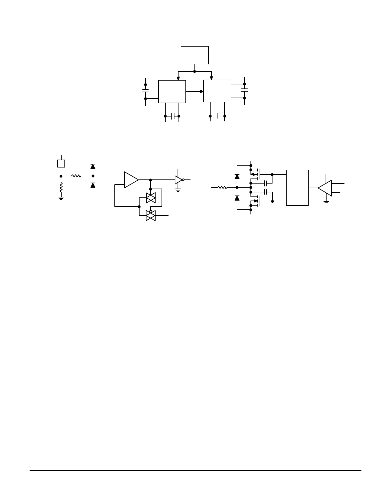
Tx
FUNCTION DIAGRAM
V
DD
V
CC
DI
1.4 V
V
SS
300
Ω
LEVEL
SHIFT
DRIVER
*
V
CC
OSC
VOLTAGE
DOUBLER
VOLTAGE
INVERTER
C3
V
DD
C1
C1 – C1 +
C2
C2 + C2 –
V
SS
GND
C4
+
+
+
+
V
CC
DO
1.0 V
1.8 V
V
SS
Rx
V
DD
5.4 k
15 k
Ω
V
DD
*Proctection circuit
RECEIVER
CHARGE PUMPS
+
–
+
–
MC145407MOTOROLA
3
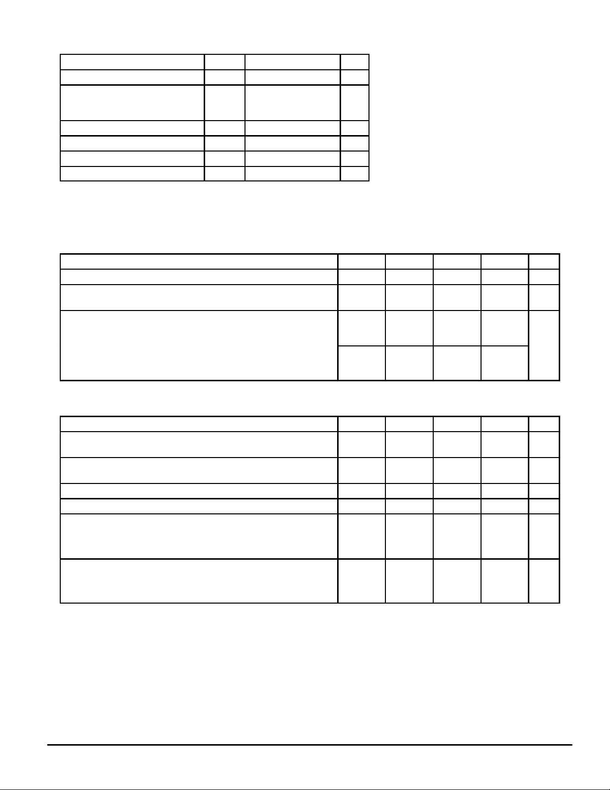
MAXIMUM RATINGS (Voltage polarities referenced to GND)
Rating
Symbol Value Unit
DC Supply Voltages V
CC
– 0.5 to + 6.0 V
Input Voltage Range
Rx1 – Rx3 Inputs
DI1 – DI3 Inputs
V
IR
VSS – 15 to VDD+ 15
– 0.5 to (VCC+ 0.5)
V
DC Current per Pin I ± 100 mA
Power Dissipation P
D
1 W
Operating Temperature Range T
A
– 40 to + 85 °C
Storage Temperature Range T
stg
– 85 to + 150 °C
DC ELECTRICAL CHARACTERISTICS (All polarities referenced to GND = 0 V; C1, C2, C3, C4 = 10 µF; T
A
= – 40 to + 85°C)
Parameter
Symbol Min Typ Max Unit
DC Supply Voltage V
CC
4.5 5 5.5 V
Quiescent Supply Current
(Outputs unloaded, inputs low)
I
CC
— 1.2 3.0 mA
Output Voltage I
load
= 0 mA
I
load
= 5 mA
I
load
= 10 mA
V
DD
8.5
7.5
6
10
9.5
9
11
—
—
V
I
load
= 0 mA
I
load
= 5 mA
I
load
= 10 mA
V
SS
– 8.5
– 7.5
– 6
– 10
– 9.2
– 8.6
–11
—
—
RECEIVER ELECTRICAL SPECIFICATIONS
(Voltage polarities referenced to GND = 0 V; VCC = + 5 V ± 10%; C1, C2, C3, C4 = 10 µF; TA = – 40 to + 85°C)
Characteristic
Symbol Min Typ Max Unit
Input Turn–on Threshold Rx1 – Rx3
V
DO1 – DO3
= V
OL
V
on
1.35 1.8 2.35 V
Input Turn–off Threshold Rx1 – Rx3
V
DO1 – DO3
= V
OH
V
off
0.75 1.0 1.25 V
Input Threshold Hysteresis (Von – V
off
) Rx1 – Rx3 V
hys
0.6 0.8 — V
Input Resistance Rx1 – Rx3 R
in
3.0 5.4 7.0 kΩ
High–Level Output Voltage DO1 – DO3
V
Rx1 – Rx3
= – 3 V to – 25 V
IOH = – 20 µA
IOH = – 1 mA
V
OH
VCC – 0.1
VCC – 0.7
—
4.3
—
—
V
Low–Level Output Voltage DO1 – DO3
V
Rx1 – Rx3
= + 3 V to + 25 V
IOL = + 20 µA
IOL = + 1.6 mA
V
OL
—
—
0.01
0.5
0.1
0.7
V
This device contains protection circuitry to
protect the inputs against damage due to high
static voltages or electric fields; however, it is
advised that normal precautions be taken to
avoid application of any voltage higher than
maximum rated voltages to this high impedance circuit. For proper operation, it is recommended that the voltages at the DI and DO pins
be constrained to the range GND ≤ VDI ≤ V
CC
and GND ≤ VDO ≤ VCC. Also, the voltage at
the Rx pin should be constrained to (V
SS
– 15 V) ≤ V
Rx1 – Rx3
≤ (VDD + 15 V), and Tx
should be constrained to VSS ≤ V
Tx1 – Tx3
≤ VDD.
Unused inputs must always be tied to
appropriate logic voltage level (e.g., GND or
VCC for DI, and GND for Rx).
 Loading...