

Motorola MC145406SD, MC145406P, MC145406DW Datasheet
MC145406
1
MOTOROLA
Driver/Receiver
EIA 232–E and CCITT V.28 (Formerly RS–232–D)
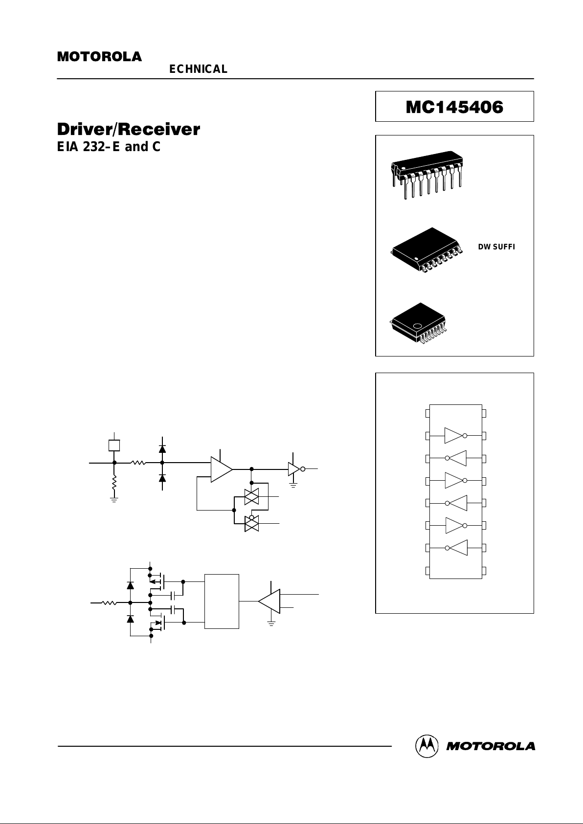
The MC145406 is a silicon–gate CMOS IC that combines three drivers
and three receivers to fulfill the electrical specifications of standards
EIA 232–E and CCITT V.28. The drivers feature true TTL input
compatibility, slew–rate–limited output, 300–Ω power–off source imped-
ance, and output typically switching to within 25% of the supply rails. The
receivers can handle up to ±25 V while presenting 3 to 7 kΩ impedance.
Hysteresis in the receivers aids reception of noisy signals. By combining
both drivers and receivers in a single CMOS chip, the MC145406 provides
efficient, low–power solutions for EIA 232–E and V.28 applications.
Drivers
•±
5 V to ±12 V Supply Range
• 300–Ω Power–Off Source Impedance
• Output Current Limiting
• TTL Compatible
• Maximum Slew Rate = 30 V/µs
Receivers
•±
25 V Input Voltage Range When V
DD
= 12 V, VSS = – 12 V
• 3 to 7 kΩ Input Impedance
• Hysteresis on Input Switchpoint
BLOCK DIAGRAM
V
DD
RECEIVER
V
CC
DO
DI
1.4 V
HYSTERESIS
1.8 V
1.0 V
DRIVER
LEVEL
SHIFT
300
Ω
Tx
V
SS
5.4 k
Rx
15 k
Ω
*Protection circuit
V
CC
V
DD
V
DD
V
CC
V
SS
+
–
+
–
*
Order this document
by MC145406/D
MOTOROLA
SEMICONDUCTOR TECHNICAL DATA
PIN ASSIGNMENT
MC145406
P SUFFIX
PLASTIC
CASE 648
DW SUFFIX
SOG
CASE 751G
1
2
3
4
5
6
7
8
9
10
11
12
13
14
15
16
R
D
V
DD
Rx1
Tx1
Rx2
Tx2
Rx3
Tx3
V
SS
V
CC
DO1
DI1
DO2
DI2
DO3
DI3
GND
D = DRIVER
R = RECEIVER
R
R
D
D
16
1
16
1
SD SUFFIX
SSOP
CASE 940B
Motorola, Inc. 1995
REV 4
1/95
MC145406
2
MOTOROLA
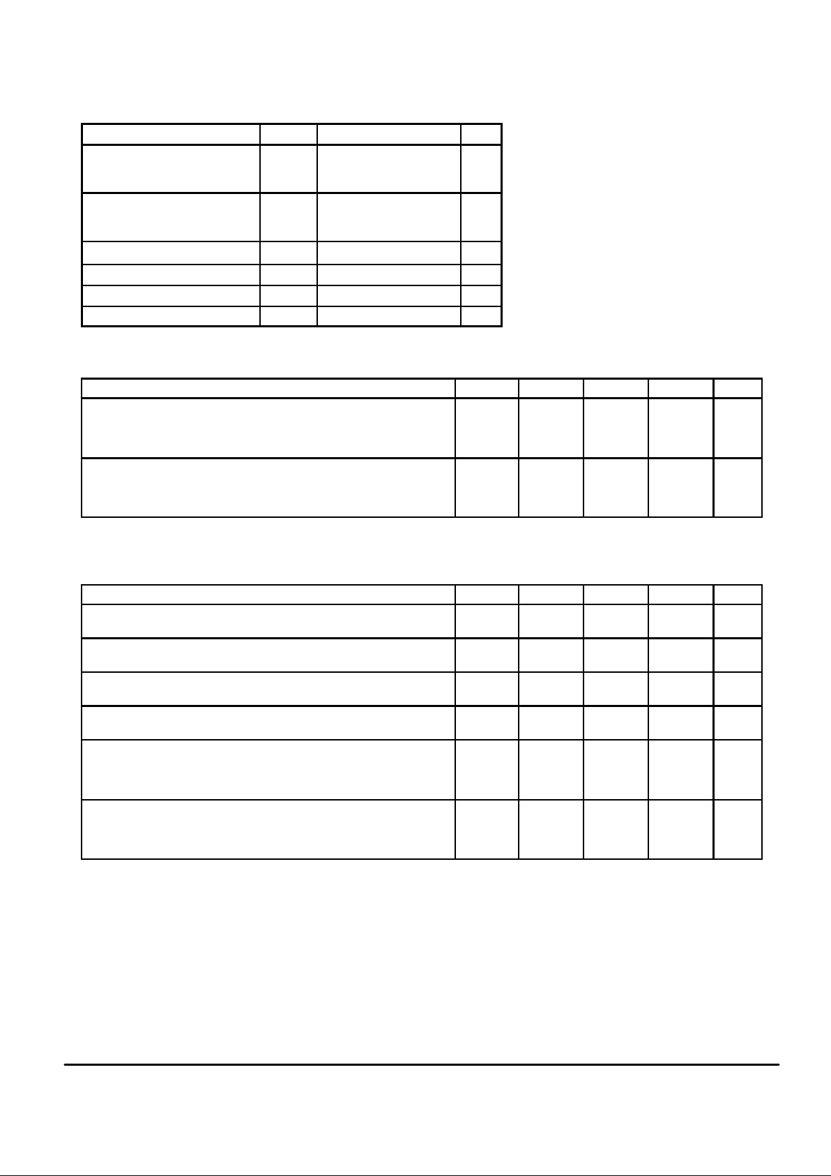
MAXIMUM RATINGS (Voltage polarities referenced to GND)
Rating Symbol Value Unit
DC Supply Voltages (VDD ≥ VCC) V
DD
V
SS
V
CC
– 0.5 to + 13.5
+ 0.5 to – 13.5
– 0.5 to + 6.0
V
Input Voltage Range
Rx1–3 Inputs
DI1–3 Inputs
V
IR
(VSS – 15) to (VDD + 15)
– 0.5 to (VCC + 0.5)
V
DC Current Per Pin
± 100
mA
Power Dissipation P
D
1.0 W
Operating Temperature Range T
A
– 40 to + 85 °C
Storage Temperature Rate T
stg
– 85 to + 150 °C
DC ELECTRICAL CHARACTERISTICS (All polarities referenced to GND = 0 V , T
A
= – 40 to +85°C)
Parameter
Symbol Min Typ Max Unit
DC Supply Voltage
V
DD
V
SS
VCC (VDD ≥ VCC)
V
DD
V
SS
V
CC
4.5
–
4.5
4.5
5 to 12
–
5 to – 12
5.0
13.2
–
13.2
5.5
V
Quiescent Supply Current (Outputs unloaded, inputs low)
VDD = + 12 V
VSS = –
12 V
VCC = + 5 V
I
DD
I
SS
I
CC
—
—
—
140
340
300
400
600
450
µA
RECEIVER ELECTRICAL SPECIFICATIONS
(Voltage polarities referenced to GND = 0 V, VDD = + 5 to + 12 V, VSS = – 5 to – 12 V, VDD ≥ VCC, TA = – 40 to + 85°C)
Characteristic
Symbol Min Typ Max Unit
Input Turn–on Threshold Rx1–Rx3
V
DO1–DO3
= VOL, VCC = 5.0 V ±
5%
V
on
1.35 1.80 2.35 V
Input Turn–off Threshold Rx1–Rx3
V
DO1–DO3
= VOH, VCC = 5.0 V ± 5%
V
off
0.75 1.00 1.25 V
Input Threshold Hysteresis Rx1–Rx3
VCC = 5.0 V
± 5%
Von–V
off
0.6 0.8 — V
Input Resistance Rx1–Rx3
(VSS –
15 V) ≤ V
Rx1–Rx3
≤ (VDD + 15 V)
R
in
3.0 5.4 7.0 kΩ
High–Level Output Voltage (V
Rx1–Rx3
= – 3 V to (VSS – 15 V))*
DO1–DO3
IOH = – 20 µA, VCC = +
5.0 V
IOH = –1 mA, VCC = +
5.0 V
V
OH
4.9
3.8
4.9
4.3
—
—
V
Low–Level Output Voltage (V
Rx1–Rx3
= + 3 V to (VDD + 15 V))* DO1–DO3
IOL = +
20 µA, V
CC
= + 5.0 V
IOL = +
2 mA, V
CC
= + 5.0 V
IOL = + 4 mA, VCC = + 5.0 V
V
OL
—
—
—
0.01
0.02
0.5
0.1
0.5
0.7
V
* This is the range of input voltages as specified by EIA 232–E to cause a receiver to be in the high or low logic state.
This device contains protection circuitry to protect the inputs against damage due to high static
voltages or electric fields; however, it is advised
that normal precautions be taken to avoid application of any voltage higher than maximum rated
voltages to this high impedance circuit. For proper
operation, it is recommended that the voltages at
the DI and DO pins be constrained to the range
GND ≤VDI≤ VCC and GND≤ VDO ≤ VCC. Also, the
voltage at the Rx pin should be constrained to
(VSS – 15 V) ≤ V
Rx1–3
≤ (VDD + 15 V), and Tx
should be constrained to VSS ≤ V
Tx1–3
≤ VDD.
Unused inputs must always be tied to an appropriate logic voltage level (e.g., GND or VCC for
DI and Ground for Rx.)
MC145406
3
MOTOROLA
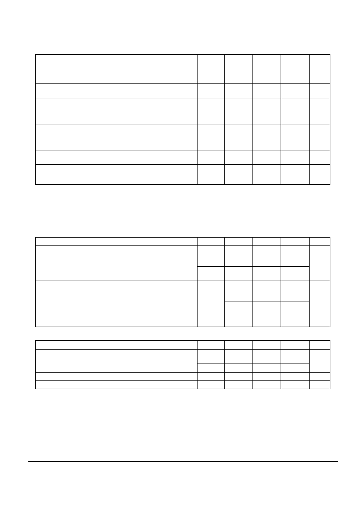
ELECTRICAL SPECIFICATIONS (Voltage polarities referenced to GND = 0 V, V
CC
= + 5 V ± 5%, TA = – 40 to + 85°C)
Characteristic
Symbol Min Typ Max Unit
Digital Input Voltage DI1–DI3
Logic 0
Logic 1
V
IL
V
IH
—
2.0
—
—
0.8
—
V
Input Current DI1–DI3
V
DI1–DI3
= V
CC
I
in
— — ± 1.0 µA
Output High Voltage (V
DI1–3
= Logic 0, RL = 3.0 kΩ) Tx1–Tx3
VDD = + 5.0 V, VSS = –
5.0 V
VDD = + 6.0 V, VSS = – 6.0
VDD = +
12.0 V, V
SS
= – 12.0 V
V
OH
3.5
4.3
9.2
3.9
4.7
9.5
—
—
—
V
Output Low Voltage* (V
DI1–3
= Logic 1, RL = 3.0 kΩ) Tx1–Tx3
VDD = + 5.0 V, VSS = – 5.0 V
VDD = + 6.0 V, VSS = – 6.0 V
VDD = +
12.0 V, V
SS
= – 12.0 V
V
OL
– 4.0
–
4.5
–
10.0
– 4.3
–
5.2
– 10.3
—
—
—
V
Off Source Resistance (Figure 1) Tx1–Tx3
VDD = VSS = GND = 0 V, V
Tx1–Tx3
= ±
2.0 V
300 — — Ω
Output Short–Circuit Current (VDD = + 12.0 V, VSS = – 12.0 V) Tx1–Tx3
Tx1–Tx3 shorted to GND**
Tx1–Tx3 shorted to ±
15.0 V***
I
SC
—
—
± 22
±
60
± 60
±
100
mA
*The voltage specifications are in terms of absolute values.
**Specification is for one Tx output pin to be shorted at a time. Should all three driver outputs be shorted simultaneously, device power dissipation
limits will be exceeded.
***This condition could exceed package limitations.
SWITCHING CHARACTERISTICS (V
CC
= + 5 V ± 5%, TA = – 40 to + 85°C; See Figures NO TAG and NO TAG)
Drivers
Characteristic Symbol Min Typ Max Unit
Propagation Delay Time Tx1–Tx3
Low–to–High
RL = 3 kΩ, CL = 50 pF
t
PLH
— 300 500
ns
High–to–Low
RL = 3 kΩ CL = 50 pF
t
PHL
— 300 500
Output Slew Rate Tx1–Tx3
Minimum Load
RL = 7 kΩ, CL = 0 pF, VDD = +
6 to + 12 V, V
SS
= – 6 to – 12 V
SR
— ± 9 ± 30
V/µs
Maximum Load
RL = 3 kΩ, CL = 2500 pF
VDD = + 12 V, VSS = – 12 V
VDD = + 5 V, VSS = – 5 V
4
—
—
—
—
—
Receivers (CL = 50 pF)
Characteristic Symbol Min Typ Max Unit
Propagation Delay Time DO1–DO3
Low–to–High
t
PLH
— 150 425
ns
High–to–Low t
PHL
— 150 425
Output Rise Time DO1–DO3 t
r
— 250 400 ns
Output Fall Time DO1–DO3 t
f
— 40 100 ns
MC145406
4
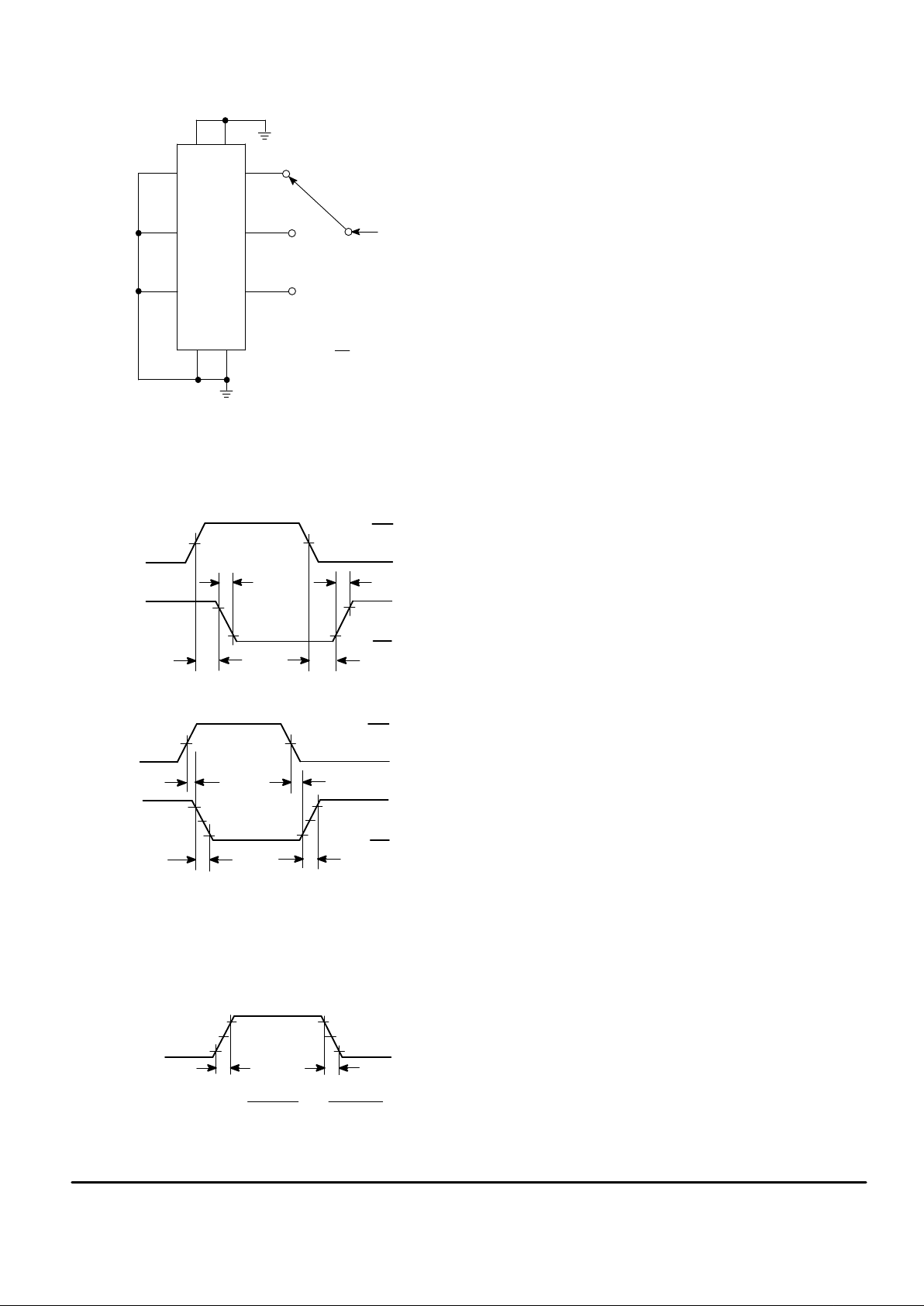
MOTOROLA
Vin = ± 2
V
3
5
7
14
12
10
89
116
VDDV
CC
DI1
DI2
DI3
V
SS
GND
Tx3
Tx2
Tx1
R
out
=
V
in
I
Figure 1. Power–Off Source Resistance (Drivers)
Figure 2. Switching Characteristics
Figure 3. Slew–Rate Characterization
DRIVERS
DI1–DI3
3 V
0 V
V
OH
V
OL
Tx1–Tx3
t
PLH
t
PHL
50%
t
f
t
r
10%
90%
RECEIVERS
Rx1–Rx3
DO1–DO3
+ 3 V
0 V
V
OH
V
OL
t
PLH
t
PHL
t
f
t
r
50%
DRIVERS
Tx1–Tx3
90%
50%
3 V
– 3 V
3 V
– 3 V
t
SHL
t
SLH
SLEW RATE (SR) =
– 3 V – (3 V)OR3 V – ( – 3 V)
t
SLH
t
SHL
10%
PIN DESCRIPTIONS
V
DD
Positive Power Supply (Pin 1)
The most positive power supply pin, which is typically + 5
to +
12V.
V
SS
Negative Power Supply (Pin 8)
The most negative power supply pin, which is typically – 5
to –
12 V.
V
CC
Digital Power Supply (Pin 16)
The digital supply pin, which is connected to the logic
power supply (maximum +
5.5 V). V
CC
must
be less than
or equal to VDD.
GND
Ground (Pin 9)
Ground return pin is typically connected to the signal
ground pin of the EIA 232–E connector (Pin 7) as well as to
the logic power supply ground.
Rx1, Rx2, Rx3
Receive Data Input (Pins 2, 4, 6)
These are the EIA 232–E receive signal inputs whose
voltages can range from (VDD + 15 V) to (VSS – 15 V). A voltage between +
3 and (V
DD
+ 15 V) is decoded as a space
and causes the corresponding DO pin to swing to ground (0
V); a voltage between – 3 and (VDD – 15 V) is decoded as a
mark and causes the DO pin to swing up to VCC. The actual
turn–on input switchpoint is typically biased at 1.8 V above
ground, and includes 800 mV of hysteresis for noise rejection. The nominal input impedance is 5 kΩ. An open or
grounded input pin is interpreted as a mark, forcing the DO
pin to VCC.
DO1, DO2, DO3
Data Output (Pins 11, 13, 15)
These are the receiver digital output pins, which swing
from VCC to GND. A space on the Rx pin causes DO to produce a logic 0; a mark produces a logic 1. Each output pin is
capable of driving one LSTTL input load.
DI1, DI2, DI3
Data Input (Pins 10, 12,14)
These are the high–impedance digital input pins to the
drivers. TTL compatibility is accomplished by biasing the input switchpoint at 1.4 V above GND. However, 5–V CMOS
compatibility is maintained as well. Input voltage levels on
these pins must be between VCC and GND.
Tx1, Tx2, Tx3
Transmit Data Output(Pins 3, 5, 7)
These are the EIA 232–E transmit signal output pins,
which swing toward VDD and VSS. A logic 1 at a DI input
causes the corresponding Tx output to swing toward VSS. A
logic 0 causes the output to swing toward VDD (the output
voltages will be slightly less than VDD or VSS depending upon
the output load). Output slew rates are limited to a maximum
of 30 V per µs. When the MC145406 is off (VDD = VSS = V
CC
= GND), the minimum output impedance is 300 Ω.
 Loading...