

Motorola MC14526BDW, MC14526BCP, MC14526BCL, MC14522BCL, MC14522BCP Datasheet
...
MOTOROLA CMOS LOGIC DATA
1
MC14522B MC14526B
The MC14522B BCD counter and the MC14526B binary counter are
constructed with MOS P–channel and N–channel enhancement mode
devices in a monolithic structure.
These devices are presettable, cascadable, synchronous down counters
with a decoded “0” state output for divide–by–N applications. In single stage
applications the “ 0” output is applied to the Preset Enable input. T he
Cascade Feedback input allows cascade divide–by–N operation with no
additional gates required. The Inhibit input allows disabling o f the pulse
counting function. Inhibit may also be used as a negative edge clock.
These complementary MOS counters can be used in frequency synthesizers, phase–locked loops, and other frequency division applications requiring
low power dissipation and/or high noise immunity.
• Supply Voltage Range = 3.0 Vdc to 18 Vdc
• Logic Edge–Clocked Design — Incremented on Positive Transition of
Clock or Negative Transition of Inhibit
• Asynchronous Preset Enable
• Capable of Driving Two Low–power TTL Loads or One Low–power
Schottky TTL Load Over the Rated Temperature Range
MAXIMUM RATINGS* (Voltages Referenced to V
SS
)
Symbol
Parameter Value Unit
V
DD
DC Supply Voltage – 0.5 to + 18.0 V
Vin, V
out
Input or Output Voltage (DC or Transient) – 0.5 to VDD + 0.5 V
Iin, I
out
Input or Output Current (DC or Transient),
per Pin
± 10 mA
P
D
Power Dissipation, per Package† 500 mW
T
stg
Storage Temperature – 65 to + 150
_
C
T
L
Lead Temperature (8–Second Soldering) 260
_
C
*Maximum Ratings are those values beyond which damage to the device may occur.
†Temperature Derating:
Plastic “P and D/DW” Packages: – 7.0 mW/_C From 65_C To 125_C
Ceramic “L” Packages: – 12 mW/_C From 100_C To 125_C
FUNCTION TABLE
Inputs Output
Clock Reset Inhibit
Preset
Enable
Cascade
Feedback
“0”
Resulting
Function
XXHHXXLHLLLHAsynchronous reset*
Asynchronous reset
X L X H X L Asynchronous preset
No change** (inactive edge)
LLL
LLLLLLNo change** (inactive edge)
No change** (inactive edge)
HLLLL
Decrement**
X = Don’t Care
NOTES:
*Output “0” is low when reset goes high only it PE and CF are low.
**Output “0” is high when reset is low, only if CF is high and count is 0000.
SEMICONDUCTOR TECHNICAL DATA
Motorola, Inc. 1995
REV 3
1/94
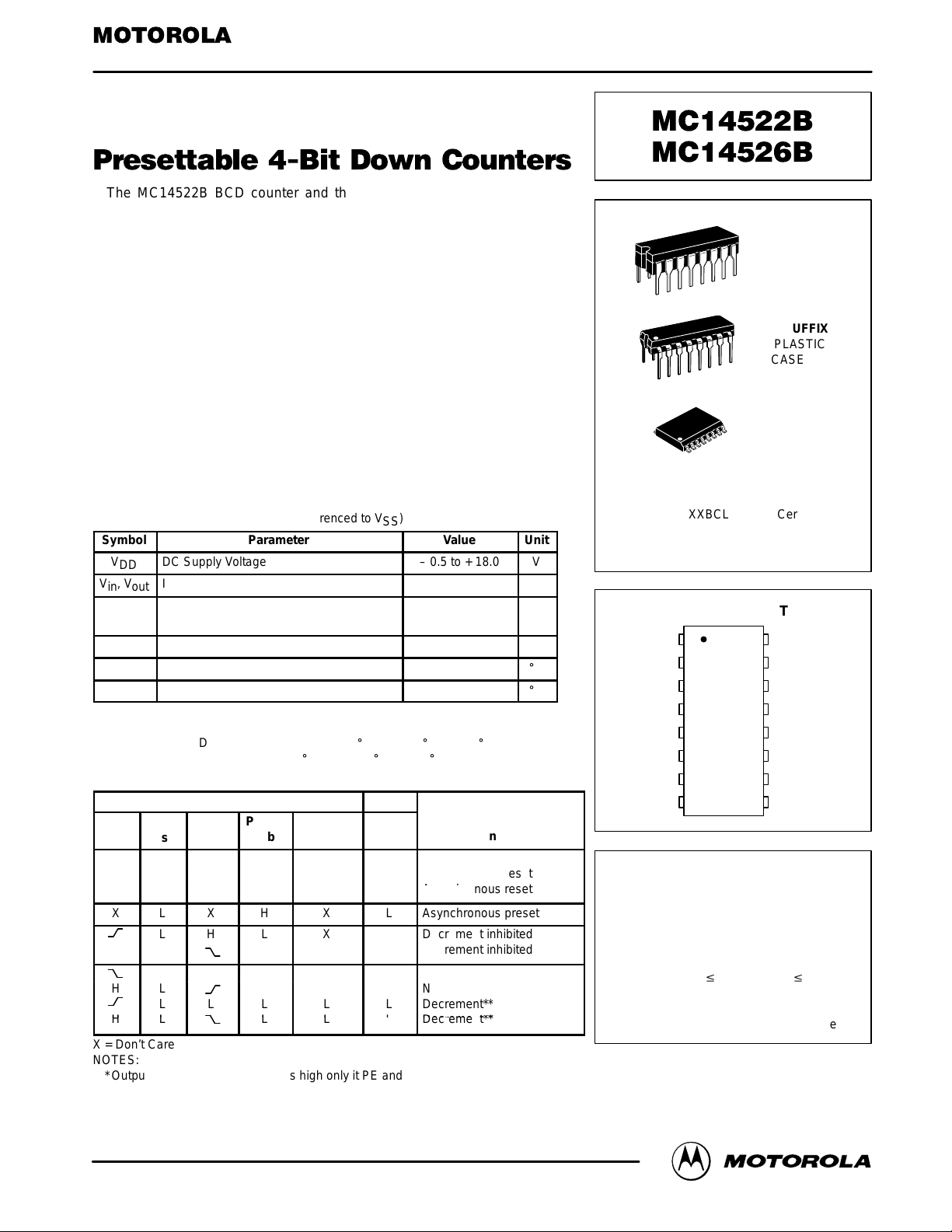
L SUFFIX
CERAMIC
CASE 620
ORDERING INFORMATION
MC14XXXBCP Plastic
MC14XXXBCL Ceramic
MC14XXXBDW SOIC
TA = – 55° to 125°C for all packages.
P SUFFIX
PLASTIC
CASE 648
DW SUFFIX
SOIC
CASE 751G
This device contains protection circuitry to
guard against damage due to high static
voltages or electric fields. However, precautions must be taken to avoid applications of
any voltage higher than maximum rated voltages to this high–impedance circuit. For proper
operation, Vin and V
out
should be constrained
to the range VSS v (Vin or V
out
) v VDD.
Unused inputs must always be tied to an
appropriate logic voltage level (e.g., either V
SS
or VDD). Unused outputs must be left open.
PIN ASSIGNMENT
13
14
15
16
9
10
11
125
4
3
2
1
8
7
6
“0”
CF
P2
Q2
V
DD
Q1
RESET
P1
INHIBIT
PE
P3
Q3
V
SS
Q0
CLOCK
P0
X
X H X X H H Asynchronous reset
L L L X L Decrement inhibited
H
H
L
L
L
X
H L
L L
L L
L
L
X
L
L
L
Asynchronous reset*
L
Decrement inhibited
L
L
Decrement**

MOTOROLA CMOS LOGIC DATAMC14522B MC14526B
2
ELECTRICAL CHARACTERISTICS (Voltages Referenced to V
SS
)
V
DD
– 55_C 25_C 125_C
Characteristic
Symbol
DD
Vdc
Min Max Min Typ # Max Min Max
Unit
“0” Level
Vin = VDD or 0
V
OL
5.0
10
15
—
—
—
0.05
0.05
0.05
—
—
—
0
0
0
0.05
0.05
0.05
—
—
—
0.05
0.05
0.05
Vdc
“1” Level
Vin = 0 or V
DD
V
OH
5.0
10
15
4.95
9.95
14.95
—
—
—
4.95
9.95
14.95
5.0
10
15
—
—
—
4.95
9.95
14.95
—
—
—
Vdc
“0” Level
(VO = 4.5 or 0.5 Vdc)
(VO = 9.0 or 1.0 Vdc)
(VO = 13.5 or 1.5 Vdc)
V
IL
5.0
10
15
—
—
—
1.5
3.0
4.0
—
—
—
2.25
4.50
6.75
1.5
3.0
4.0
—
—
—
1.5
3.0
4.0
Vdc
“1” Level
(VO = 0.5 or 4.5 Vdc)
(VO = 1.0 or 9.0 Vdc)
(VO = 1.5 or 13.5 Vdc)
V
IH
5.0
10
15
3.5
7.0
11
—
—
—
3.5
7.0
11
2.75
5.50
8.25
—
—
—
3.5
7.0
11
—
—
—
Vdc
I
OH
5.0
5.0
10
15
– 3.0
– 0.64
– 1.6
– 4.2
—
—
—
—
– 2.4
– 0.51
– 1.3
– 3.4
– 4.2
– 0.88
– 2.25
– 8.8
—
—
—
—
– 1.7
– 0.36
– 0.9
– 2.4
—
—
—
—
mAdc
I
OL
5.0
10
15
0.64
1.6
4.2
—
—
—
0.51
1.3
3.4
0.88
2.25
8.8
—
—
—
0.36
0.9
2.4
—
—
—
mAdc
Input Current I
in
15 — ± 0.1 — ±0.00001 ± 0.1 — ± 1.0 µAdc
Input Capacitance
(Vin = 0)
C
in
— — — — 5.0 7.5 — — pF
Quiescent Current
(Per Package)
I
DD
5.0
10
15
—
—
—
5.0
10
20
—
—
—
0.005
0.010
0.015
5.0
10
20
—
—
—
150
300
600
µAdc
Total Supply Current**†
(Dynamic plus Quiescent,
Per Package)
(CL = 50 pF on all outputs, all
buffers switching)
I
T
5.0
10
15
IT = (1.7 µA/kHz) f + I
DD
IT = (3.4 µA/kHz) f + I
DD
IT = (5.1 µA/kHz) f + I
DD
µAdc
#Data labelled “Typ” is not to be used for design purposes but is intended as an indication of the IC’s potential performance.
**The formulas given are for the typical characteristics only at 25_C.
†To calculate total supply current at loads other than 50 pF:
IT(CL) = IT(50 pF) + (CL – 50) Vfk
where: IT is in µA (per package), CL in pF, V = (VDD – VSS) in volts, f in kHz is input frequency, and k = 0.001.
Output Voltage
Input Voltage
Output Drive Current
(VOH = 2.5 Vdc) Source
(VOH = 4.6 Vdc)
(VOH = 9.5 Vdc)
(VOH = 13.5 Vdc)
(VOL = 0.4 Vdc) Sink
(VOL = 0.5 Vdc)
(VOL = 1.5 Vdc)

MOTOROLA CMOS LOGIC DATA
3
MC14522B MC14526B
SWITCHING CHARACTERISTICS* (C
L
= 50 pF, TA = 25_C)
Characteristic
Symbol V
DD
Min Typ # Max Unit
Output Rise and Fall Time
t
TLH
, t
THL
= (1.5 ns/pF) CL + 25 ns
t
TLH
, t
THL
= (0.75 ns/pF) CL + 12.5 ns
t
TLH
, t
THL
= (0.55 ns/pF) CL + 9.5 ns
t
TLH
,
t
THL
(Figures 4, 5)
5.0
10
15
—
—
—
100
50
40
200
100
80
ns
5.0
10
15
—
—
—
550
225
160
1100
450
320
5.0
10
15
—
—
—
240
130
100
480
260
200
Propagation Delay Time
Pn to Q
t
PLH
,
t
PHL
(Figures 4, 7)
5.0
10
15
—
—
—
260
120
100
520
240
200
ns
Propagation Delay Time
Reset to Q
t
PHL
(Figure 8)
5.0
10
15
—
—
—
250
110
80
500
220
160
ns
Propagation Delay Time
Preset Enable to “0”
t
PHL
,
t
PLH
(Figures 4, 9)
5.0
10
15
—
—
—
220
100
80
440
200
160
ns
Clock or Inhibit Pulse Width t
w
(Figures 5, 6)
5.0
10
15
250
100
80
125
50
40
—
—
—
ns
Clock Pulse Frequency (with PE = low) f
max
(Figures 4, 5, 6)
5.0
10
15
—
—
—
2.0
5.0
6.6
1.5
3.0
4.0
MHz
Clock or Inhibit Rise and Fall Time tr,
t
f
(Figures 5, 6)
5.0
10
15
—
—
—
—
—
—
15
5
4
µs
Setup Time
Pn to Preset Enable
t
su
(Figure 10)
5.0
10
15
90
50
40
40
15
10
—
—
—
ns
Hold Time
Preset Enable to Pn
t
h
(Figure 10)
5.0
10
15
30
30
30
– 15
– 5
0
—
—
—
ns
Preset Enable Pulse Width t
w
(Figure 10)
5.0
10
15
250
100
80
125
50
40
—
—
—
ns
Reset Pulse Width t
w
(Figure 8)
5.0
10
15
350
250
200
175
125
100
—
—
—
ns
Reset Removal Time t
rem
(Figure 8)
5.0
10
15
10
20
30
– 110
– 30
– 20
—
—
—
ns
*The formulas given are for the typical characteristics only at 25_C.
#Data labelled “Typ” is not to be used for design purposes but is intended as an indication of the IC’s potential performance.
Propagation Delay Time (Inhibit Used as Negative
Edge Clock)
Clock or Inhibit to Q
t
PLH
t
PLH
t
PLH
Clock or Inhibit to “0”
t
PLH
t
PLH
t
PLH
, t
= (1.7 ns/pF) CL + 465 ns
PHL
, t
= (0.66 ns/pF) CL + 197 ns
PHL
, t
= (0.5 ns/pF) CL + 135 ns
PHL
, t
= (1.7 ns/pF) CL + 155 ns
PHL
, t
= (0.66 ns/pF) CL + 87 ns
PHL
, t
= (0.5 ns/pF) CL + 65 ns
PHL
(Figures 4, 5, 6)
t
,
PLH
t
PHL
ns
 Loading...