

Motorola MC12040AP Datasheet
Device
Operating
Temperature Range
Package
SEMICONDUCTOR
TECHNICAL DATA
PHASE–FREQUENCY
DETECTOR
ORDERING INFORMATION
MC12040P TA = 0° to +75°C Plastic
FN SUFFIX
PLASTIC PACKAGE
CASE 775
(PLCC)
PIN CONNECTIONS
Order this document by MC12040/D
3
19
4
8
Not Recommended for New Designs
14
1
P SUFFIX
PLASTIC PACKAGE
CASE 646
V
ref
NC
Compensation
(Top View)
NC
Voltage Feedback
NC
Current Sense
NC
RT/C
T
V
CC
V
C
Output
Gnd
Power Ground
1
2
3
4
14
13
12
11
5
6
7
10
9
8
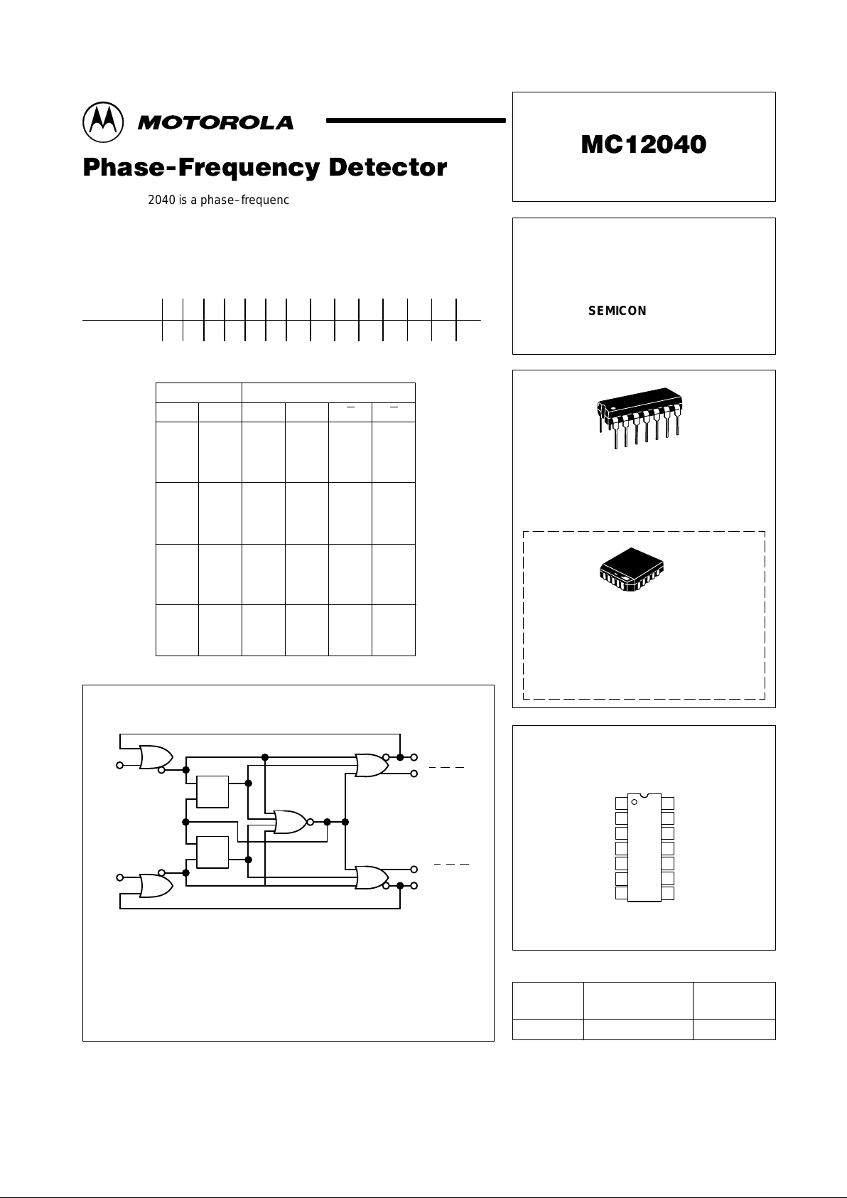
The MC12040 is a phase–frequency detector intended for use in systems
requiring zero phase and frequency difference at lock. In combination with a
voltage controlled oscillator (such as the MC1648, MC12147, MC12148 or
MC12149), it is useful in a broad range of phase–locked loop applications.
• Operating Frequency = 80 MHz Typical
Pin Conversion Table
14 PIN DIP 1 2 3 4 5 6 7 8 9 10 11 12 13 14
20 PIN PLCC 2 3 4 6 8 9 10 12 13 14 16 18 19 20
LOGIC DIAGRAM
R
S
Q
S
RQ
R 6
V 9
4 U (fR>fV)
3 U
(fR>fV)
12 D
(fV>fR)
11 D (fV>fR)
V
CC1
= Pin 1
V
CC2
= Pin 14
VEE = Pin 7
TRUTH TABLE
This is not strictly a functional truth table; i.e., it does not cover all possible
modes of operation. However, it gives a sufficient number of tests to
ensure that the device will function properly in all modes of operation.
0
0
1
0
R
1
0
1
1
1
1
1
1
1
0
1
0
1
1
1
V
1
1
1
0
1
0
1
0
1
1
1
X
X
X
X
U
1
1
1
1
0
0
0
0
0
0
0
X
X
X
X
D
0
0
0
0
0
0
1
1
1
1
0
X
X
X
X
U
0
0
0
0
1
1
1
1
1
1
1
X
X
X
X
D
1
1
1
1
1
1
0
0
0
0
1
Inputs
Outputs
Motorola, Inc. 1997 Rev 3
MC12040
2
MOTOROLA RF/IF DEVICE DATA
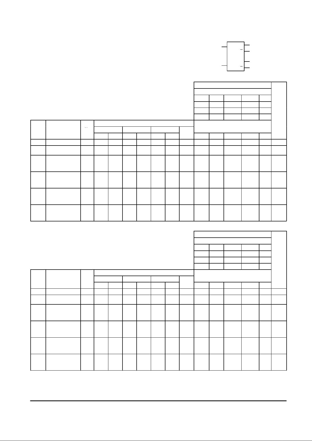
ELECTRICAL CHARACTERISTICS
The MC12040 has been designed to meet the dc
specifications shown in the test table after thermal
equilibrium has been established. Outputs are terminated
through a 50 ohm resistor to +3.0 V for +5.0 V tests and
through a 50 ohm resistor to –2.0 V for –5.2 V tests.
6 R
9V
U4
D12
D11
U3
TEST VOLTAGE VALUES
(Volts)
@ Test Temperature V
IHmaxVILminVIHAminVILAmaxVEE
0°C –0.840 –1.870 –1.145 –1.490 –5.2
25°C –0.810 –1.850 –1.105 –1.475 –5.2
Supply Voltage = –5.2V 75°C –0.720 –1.830 –1.045 –1.450 –5.2
MC12040
Pin
0°C 25°C 75°C
TEST VOLTAGE APPLIED TO PINS BELOW
Symbol Characteristics
Und
er
Test
Min Max Min Max Min Max
Unit
V
IHmaxVILminVIHAminVILAmaxVEE
(VCC)
Gnd
I
E
Power Supply Drain 7 –120 –60 mAdc 7 1,14
I
INH
Input Current 6
9
350
350
µAdc 6
9
771,14
1,14
V
OH
1
Logic “1”
Output Voltage
3
4
11
12
–1.000 –0.840 –0.960 –0.810 –0.900 –0.720
Vdc
7 1,14
V
OL
1
Logic “0”
Output Voltage
3
4
11
12
–1.870 –1.635 –1.850 –1.620 –1.830 –1.595
Vdc
7 1,14
V
OHA
2
Logic “1”
Input Voltage
3
4
11
12
–1.020 –0.980 –0.920
Vdc
6.9 7 1,14
V
OLA
2
Logic “0”
Input Voltage
3
4
11
12
–1.615 –1.600 –1.575
Vdc 9
6
9
6
6
9
6
9
7 1,14
TEST VOLTAGE VALUES
(Volts)
@ Test Temperature V
IHmaxVILminVIHAminVILAmaxVEE
0°C +4.160 +3.130 +3.855 +3.510 +5.0
25°C +4.190 +3.150 +3.895 +3.525 +5.0
Supply Voltage = +5.0V 75°C +4.280 +3.170 +3.955 +3.550 +5.0
MC12040
Pin
0°C 25°C 75°C
TEST VOLTAGE APPLIED TO PINS BELOW
(V
)
Symbol Characteristics
Und
er
Test
Min Max Min Max Min Max
Unit
V
IHmaxVILminVIHAminVILAmaxVEE
(VCC)
Gnd
I
E
Power Supply Drain 7 –115 –60 mAdc 1,14 7
I
INH
Input Current 6
9
350
350
µAdc 6
9
1,14
1,1477
V
OH
1
Logic “1”
Output Voltage
3
4
11
12
4.000 4.160 4.040 4.190 4.100 4.280
Vdc
1,14 7
V
OL
1
Logic “0”
Output Voltage
3
4
11
12
3.190 3.430 3.210 3.440 3.230 3.470
Vdc
1,14 7
V
OHA
2
Logic “1”
Input Voltage
3
4
11
12
3.980 4.020 4.080
Vdc
6.9 1,14 7
V
OLA
2
Logic “0”
Input Voltage
3
4
11
12
3.450 3.460 3.490
Vdc 9
6
9
6
6
9
6
9
1,14 7
NOTE: For more information on using an ECL device in a
+5V system, refer to Motorola Application Note
AN1406/D, “Designing with PECL (ECL at +5.0V)”
 Loading...