

MOTOROLA MC10H641FNR2, MC100H641FN, MC100H641FNR2 Datasheet
MOTOROLA
SEMICONDUCTOR TECHNICAL DATA
Single Supply PECL-TTL
1:9 Clock Distribution Chip
The MC10H/100H641 is a single supply , low skew translating 1:9 clock
driver. Devices in the Motorola H600 translator series utilize the 28–lead
PLCC for optimal power pinning, signal flow through and electrical
performance.
The device features a 24mA TTL output stage, with AC performance
specified into a 50pF load capacitance. A latch is provided on–chip. When
LEN is LOW (or left open, in which case it is pulled LOW by the internal
pulldown) the latch is transparent. A HIGH on the enable pin (EN
all outputs LOW. Both the LEN and EN
The VBB output is provided in case the user wants to drive the device
with a single–ended input. For single–ended use the VBB should be
connected to the D
The 10H version of the H641 is compatible with positive MECL 10H
logic levels. The 100H version is compatible with positive 100K levels.
input and bypassed with a 0.01µF capacitor.
pins are positive ECL inputs.
• PECL–TTL Version of Popular ECLinPS E111
• Low Skew
• Guaranteed Skew Spec
• Latched Input
• Differential ECL Internal Design
• V
Output for Single–Ended Use
BB
• Single +5V Supply
• Logic Enable
• Extra Power and Ground Supplies
• Separate ECL and TTL Supply Pins
) forces
MC10H641
MC100H641
SINGLE SUPPLY
PECL–TTL 1:9 CLOCK
DISTRIBUTION CHIP
FN SUFFIX
PLASTIC PACKAGE
CASE 776–02
Pinout: 28–Lead PLCC (Top View)
GT Q6 VT Q7 VT Q8 GTGT Q6 VT Q7 VT Q8 GT
25 24 23 22 21 20 19
GT
26
Q5
27
VT
28
Q4
1
VT
2
Q3
3
GT
4
567891011
GT Q2 VT Q1 VT Q0 GT
MECL 10H is a trademark of Motorola, Inc.
11/93
Motorola, Inc. 1996
2–1
PIN NAMES
VBB
18
D
17
16
D
15
VE
14
LEN
13
GE
12
EN
Pins
GT, VT
GE, VE
D, D
V
BB
Q0–Q8
EN
LEN
REV 3
Function
TTL GND, TTL V
ECL GND, ECL V
Signal Input (Positive ECL)
VBB Reference Output
(Positive ECL)
Signal Outputs (TTL)
Enable Input (Positive ECL)
Latch Enable Input
(Positive ECL)
CC
CC
MC10H641 MC100H641
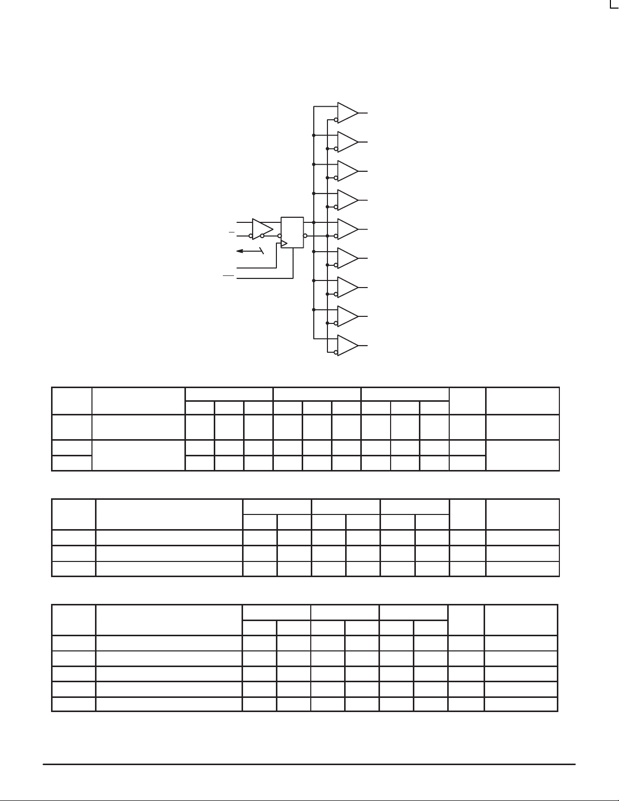
LOGIC DIAGRAM
TTL Outputs
Q0
Q1
Q2
PECL Input
D
D
VBB
LEN
EN
DQ
Q3
Q4
Q5
Q6
Q7
Q8
DC CHARACTERISTICS (VT = VE = 5.0V ±5%)
TA = 0°C TA = + 25°C TA = + 85°C
Symbol Characteristic Min Typ Max Min Typ Max Min Typ Max Unit Condition
I
EE
I
CCH
I
CCL
Power Supply Current
PECL
TTL 24 30 24 30 24 30 mA
24 30 24 30 24 30 mA
27 35 27 35 27 35 mA
TTL DC CHARACTERISTICS (VT = VE = 5.0V ±5%)
0°C 25°C 85°C
Symbol Characteristic Min Max Min Max Min Max Unit Condition
V
V
I
OH
OL
OS
Output HIGH Voltage 2.5 2.5 2.5 V IOH = –15mA
Output LOW Voltage 0.5 0.5 0.5 V IOL = 24mA
Output Short Circuit Current –100 –225 –100 –225 –100 –225 mA V
OUT
= 0V
10H PECL DC CHARACTERISTICS
0°C 25°C 85°C
Symbol Characteristic Min Max Min Max Min Max Unit Condition
I
IH
I
IL
V
IH
V
IL
V
BB
1. PECL VIH, VIL, and VBB are referenced to VE and will vary 1:1 with the power supply. The levels shown are for VE = 5.0V.
MOTOROLA MECL Data
Input HIGH Current 225 175 175 µA
Input LOW Current 0.5 0.5 0.5 µA
Input HIGH Voltage 3.83 4.16 3.87 4.19 3.94 4.28 V VE = 5.0V
Input LOW Voltage 3.05 3.52 3.05 3.52 3.05 3.55 V VE = 5.0V
Output Reference Voltage 3.62 3.73 3.65 3.75 3.69 3.81 V VE = 5.0V
2–2
DL122 — Rev 6
1
1
1
MC10H641 MC100H641
100H PECL DC CHARACTERISTICS
0°C 25°C 85°C
Symbol Characteristic Min Max Min Max Min Max Unit Condition
I
IH
I
IL
V
IH
V
IL
V
BB
1. PECL VIH, VIL, and VBB are referenced to VE and will vary 1:1 with the power supply. The levels shown are for VE = 5.0V.
AC CHARACTERISTICS (VT = VE = 5.0V ±5%)
Symbol Characteristic Min Typ Max Min Typ Max Min Typ Max Unit Condition
t
PLH
t
PHL
t
skew
t
PLH
t
PHL
t
PLH
t
PHL
t
r
t
f
f
MAX
t
REC
t
S
t
H
1. Propagation delay measurement guaranteed for junction temperatures. Measurements performed at 50MHz input frequency.
2. Skew window guaranteed for a single temperature across a VCC = VT = VE of 4.75V to 5.25V (See Application Note in this datasheet).
3. Skew window guaranteed for a single temperature and single VCC = VT = V
4. Output–to–output skew is specified for identical transitions through the device.
5. Frequency at which output levels will meet a 0.8V to 2.0V minimum swing.
Input HIGH Curren 225 175 175 µA
Input LOW Current 0.5 0.5 0.5 µA
Input HIGH Voltage 3.835 4.120 3.835 4.120 3.835 4.120 V VE = 5.0V
Input LOW Voltage 3.190 3.525 3.190 3.525 3.190 3.525 V VE = 5.0V
Output Reference Voltage 3.62 3.74 3.62 3.74 3.62 3.74 V VE = 5.0V
TJ = 0°C TJ = + 25°C TJ = + 85°C
Propagation Delay
D to Q
Device Skew
Part–to–Part
Single V
CC
Output–to–Output
Propagation Delay
LEN to Q
Propagation Delay
to Q
EN
Output Rise/Fall
0.8V to 2.0V
Max Input Frequency 65 65 65 MHz CL = 50 pF
Recovery Time EN 1.25 1.25 1.25 ns
Setup Time 0.75 0.50 0.75 0.50 0.75 0.50 ns
Hold Time 0.75 0.50 0.75 0.50 0.75 0.50 ns
5.00
5.50
6.00
4.86
5.36
5.86
5.08
5.58
5.36
5.86
6.36
5.27
5.77
6.27
5.43
1000
750
350
4.9 6.9 4.9 6.9 5.0 7.0 ns CL = 50 pF
5.0 7.0 4.9 6.9 5.0 7.0 ns CL = 50 pF
1.7
1.6
1000
750
350
1.7
1.6
E
5.93
6.08
6.43
1000
750
350
1.7
1.6
ns CL = 50 pF
ps
CL = 50pF
CL = 50 pF
CL = 50 pF
ns CL = 50 pF
1
1
1
1
2
3
4
5
DETERMINING SKEW FOR A SPECIFIC APPLICATION
The H641 has been designed to meet the needs of very low
skew clock distribution applications. In order to optimize the
device for this application special considerations are
necessary in the determining of the part–to–part skew
specification limits. Older standard logic devices are specified
with relatively slack limits so that the device can be
guaranteed over a wide range of potential environmental
conditions. This range of conditions represented all of the
potential applications in which the device could be used. The
result was a specification limit that in the vast majority of cases
was extremely conservative and thus did not allow for an
optimum system design. For non–critical skew designs this
practice is acceptable, however as the clock speeds of
DL122 — Rev 6
systems increase overly conservative specification limits can
kill a design.
The following will discuss how users can use the
information provided in this data sheet to tailor a part–to–part
skew specification limit to their application. The skew
determination process may appear somewhat tedious and
time consuming, however if the utmost in performance is
required this procedure is necessary. For applications which
do not require this level of skew performance a generic
part–to–part skew limit of 2.5ns can be used. This limit is good
for the entire ambient temperature range, the guaranteed V
(VT, VE) range and the guaranteed operating frequency range.
2–3 MOTOROLAMECL Data
CC
 Loading...