

MOTOROLA MC10H640FNR2, MC100H640FNR2 Datasheet
MOTOROLA
SEMICONDUCTOR TECHNICAL DATA
68030/040
PECL-TTL Clock Driver
The MC10H/100H640 generates the necessary clocks for the 68030,
68040 and similar microprocessors. It is guaranteed to meet the clock
specifications required by the 68030 and 68040 in terms of part–to–part
skew, within–part skew and also duty cycle skew.
The user has a choice of using either TTL or PECL (ECL referenced to
+5.0V) for the input clock. TTL clocks are typically used in present MPU
systems. However, as clock speeds increase to 50MHz and beyond, the
inherent superiority of ECL (particularly differential ECL) as a means of
clock signal distribution becomes increasingly evident. The H640 also
uses differential PECL internally to achieve its superior skew
characteristic.
The H640 includes divide–by–two and divide–by–four stages, both to
achieve the necessary duty cycle skew and to generate MPU clocks as
required. A typical 50MHz processor application would use an input clock
running at 100MHz, thus obtaining output clocks at 50MHz and 25MHz
(see Logic Symbol).
The 10H version is compatible with MECL 10H ECL logic levels,
while the 100H version is compatible with 100K levels (referenced
to +5.0V).
• Generates Clocks for 68030/040
• Meets 030/040 Skew Requirements
• TTL or PECL Input Clock
• Extra TTL and PECL Power/Ground Pins
• Asynchronous Reset
• Single +5.0V Supply
MC10H640
MC100H640
68030/040
PECL–TTL CLOCK
DRIVER
FN SUFFIX
PLASTIC PACKAGE
CASE 776–02
Function
Reset (R):
Power–Up:
Select (SEL):
The H640 also contains circuitry to force a stable state of the ECL input differential pair, should both sides be left open. In this
case, the DE side of the input is pulled LOW, and DE
LOW on RESET forces all Q outputs LOW and all Q outputs HIGH.
The device is designed to have the POS edges of the ÷2 and ÷4 outputs synchronized at power up.
LOW selects the ECL input source (DE/DE). HIGH selects the TTL input source (DT).
goes HIGH.
VT VT Q1 GT GT Q0 VT
25 24 23 22 21 20 19
18
Q2
GT
GT
VT
VT
Q3
26
27
28
1
2
3
4
Pinout: 28–Lead PLCC
(Top View)
567891011
Q1
GT GT Q4 Q5 VT SEL
V
BB
17
DE
16
DE
VE
15
R
14
GE
13
12
DTQ0
11/93
Motorola, Inc. 1996
2–1
REV 3
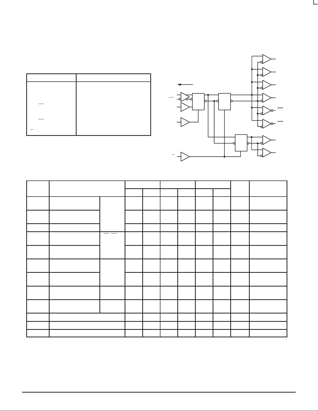
MC10H640 MC100H640
LOGIC DIAGRAM
TTL Outputs
Q0
PIN NAMES
TTL/ECL Clock Inputs
V
BB
DE
DE
DT
SEL
MUX
÷ 2
÷ 4
GT
VT
VE
GE
DE, DE
V
BB
DT
Qn, Qn
SEL
R
PIN FUNCTION
TTL Ground (0 V)
TTL VCC (+5.0 V)
ECL VCC (+5.0 V)
ECL Ground (0 V)
ECL Signal Input (positive ECL)
VBB Reference Output
TTL Signal Input
Signal Outputs (TTL)
Input Select (TTL)
Reset (TTL)
TTL Control Inputs
R
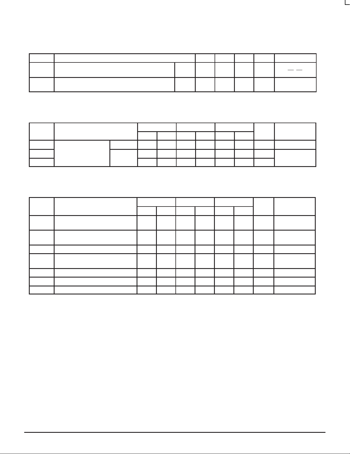
AC CHARACTERISTICS (VT = VE = 5.0V ±5%)
0°C 25°C 85°C
Symbol Characteristic Min Max Min Max Min Max Unit Condition
t
PLH
t
PLH
tskwd* Within–Device Skew 0.5 0.5 0.5 ns CL = 25pF
t
PLH
t
PLH
t
PLH
t
PLH
t
PD
t
R
t
F
f
max
t
pw
t
rr
* Within–Device Skew defined as identical transitions on similar paths through a device.
Propagation Delay ECL
D to Output
Propagation Delay TTL
D to Output
Propagation Delay ECL
D to Output
Propagation Delay TTL
D to Output
Propagation Delay ECL
D to Output
Propagation Delay TTL
D to Output
Propagation Delay
R to Output
Output Rise/Fall Time
0.8 V – 2.0 V
Maximum Input Frequency 135 135 135 MHz CL = 25pF
Minimum Pulse Width 1.50 1.50 1.50 ns
Reset Recovery Time 1.25 1.25 1.25 ns
Q0–Q3 4.9 5.9 4.9 5.9 5.2 6.2 ns CL = 25pF
5.0 6.0 5.0 6.0 5.3 6.3 ns CL = 25pF
Q0, Q1 4.9 5.9 4.9 5.9 5.2 6.2 ns CL = 25pF
5.0 6.0 5.0 6.0 5.3 6.3 ns CL = 25pF
Q4, Q5 4.9 5.9 4.9 5.9 5.2 6.2 ns CL = 25pF
5.0 6.0 5.0 6.0 5.3 6.3 ns CL = 25pF
All
Outputs
All
Outputs
4.3 6.3 4.3 6.3 5.0 7.0 ns CL = 25pF
2.5
2.5
2.5
2.5
2.5
2.5
ns CL = 25pF
Q1
Q2
Q3
Q0
Q1
Q4
Q5
MOTOROLA MECL Data
2–2
DL122 — Rev 6
MC10H640 MC100H640
VCC and CLOAD RANGES TO MEET DUTY CYCLE REQUIREMENTS (0°C ≤ TA ≤ 85°C Output Duty Cycle Measured
Relative to 1.5V)
Symbol Characteristic Min Nom Max Unit Condition
Range of VCC and CL to meet minimum pulse width
(HIGH or LOW) = 11.5 ns at f
Range of VCC and CL to meet minimum pulse width
(HIGH or LOW) = 9.5 ns at 40 < f
≤ 40 MHz
out
out
≤ 50 MHz
DC CHARACTERISTICS (VT = VE = 5.0 V ±5%)
0°C 25°C 85°C
Symbol Characteristic Min Max Min Max Min Max Unit Condition
I
EE
I
CCH
I
CCL
Power Supply Current ECL 57 57 57 mA VE Pin
TTL 30 30 30 mA Total all VT pins
V
CC
CL
V
CC
CL
30 30 30 mA
4.75
10
4.875155.0 5.125
5.0 5.25
50
27
V
pF
V
pF
Q0–Q3
–Q1
Q0
Q0–Q3
TTL DC CHARACTERISTICS (VT = VE = 5.0 V ±5%)
0°C 25°C 85°C
Symbol Characteristic Min Max Min Max Min Max Unit Condition
V
V
I
I
V
V
V
I
IH
IL
IH
IL
OH
OL
IK
OS
Input HIGH Voltage
Input LOW Voltage
Input HIGH Current 20
Input LOW Current –0.6 –0.6 –0.6 mA VIN = 0.5V
Output HIGH Voltage 2.5
Output LOW Voltage 0.5 0.5 0.5 V IOL = 24mA
Input Clamp Voltage –1.2 –1.2 –1.2 V IIN = –18mA
Output Short Circuit Current –100 –225 –100 –225 –100 –225 mA V
2.0
2.0
0.8
100
2.0
2.5
2.0
0.8
20
100
2.0
2.5
2.0
0.8
20
100
V
µA VIN = 2.7V
VIN = 7.0V
V IOH = –3.0mA
IOH = –15mA
= 0V
OUT
DL122 — Rev 6
2–3 MOTOROLAMECL Data
 Loading...