

Motorola MC10H330FNR2, MC10H330L, MC10H330P, MC10H330FN Datasheet
SEMICONDUCTOR TECHNICAL DATA
!
"
The MC10H330 is a Quad Bus Driver/Receiver with two–to–one output
multiplexers. These multiplexers have a common select and output enable.
When disabled, (OE
brought to a low state (VOL) by applying a high level to the receiver enable (RE
= High). The parameters specified are with 25 Ω loading on the bus drivers and
50 Ω loads on the receivers.
• Propagation Delay, 1.5 ns Typical Data–to–Output
• Improved Noise Margin 150 mV (Over Operating Voltage and
Temperature Range)
• Voltage Compensated
• MECL 10K–Compatible
MAXIMUM RATINGS
Power Supply (VCC = 0) V
Input Voltage (VCC = 0) V
Output Current— Continuous
Operating Temperature Range T
Storage Temperature Range— Plastic
ELECTRICAL CHARACTERISTICS (VEE = –5.2 V ±5%) (See Note)
Characteristic Symbol Min Max Min Max Min Max Unit
Power Supply Current I
Input Current High
Pins 5–8, 17–20
Pins 16, 21
Pin 9
Input Current Low I
High Output Voltage V
Low Output Voltage V
High Input Voltage V
Low Input Voltage V
AC PARAMETERS
Propagation Delay
Select–to–Input
Data–to–Bus Output
Select–to–Bus
Output
OE
–to–Bus Output
Bus–to–Input
RE
–to–Input
Data–to–Receiver
Input
Rise Time t
Fall Time t
= high) the bus outputs go to –2.0 V. Their output can be
Characteristic Symbol Rating Unit
–8.0 to 0 Vdc
0 to V
EE
50
100
0 to +75 °C
–55 to +150
–55 to +165
417
321
297
5.3
2.0
3.2
2.2
2.1
2.2
4.0
—
—
—
1.8
0.5
1.0
0.8
0.8
0.5
1.3
Vdc
mA
°C
°C
417
321
297
5.3
2.0
3.2
2.2
2.4
2.2
4.0
— Surge
EE
I
I
out
A
T
667
514
475
5.3
2.0
3.2
2.2
2.1
2.2
4.0
stg
—
—
—
1.8
0.5
1.0
0.8
0.8
0.5
1.3
— Ceramic
0° 25° 75°
— 157 — 143 — 157 mA
—
—
—
0.5 — 0.5 — 0.3 — µA
–1.02 –0.84 –0.98 –0.81 –0.92 –0.735 Vdc
–1.95 –1.63 –1.95 –1.63 –1.95 –1.60 Vdc
–1.17 –0.84 –1.13 –0.81 –1.07 –0.735 Vdc
–1.95 –1.48 –1.95 –1.48 –1.95 –1.45 Vdc
IL
1.8
0.5
1.0
0.8
0.8
0.5
1.3
0.5 2.0 0.5 2.0 0.5 2.0 ns
r
0.5 2.0 0.5 2.0 0.5 2.0 ns
f
I
t
E
inH
inL
OH
OL
IH
pd
µA
ns
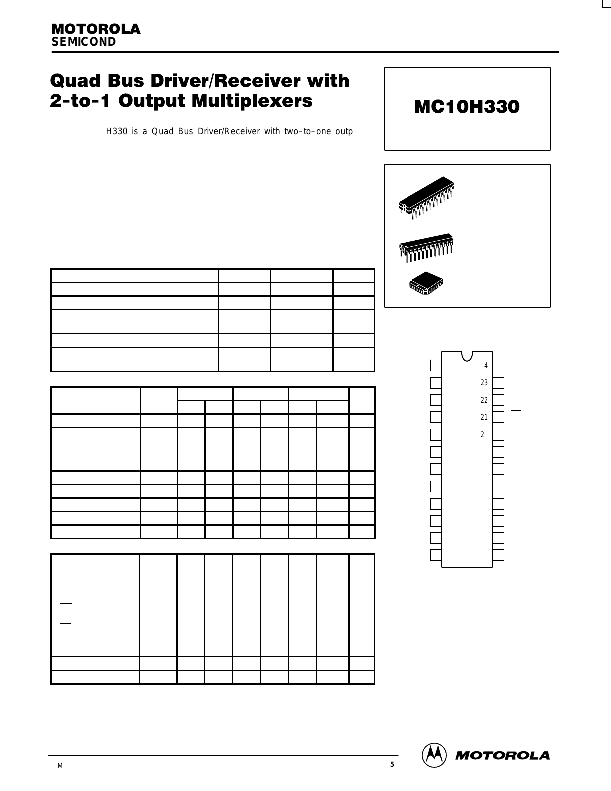
L SUFFIX
CERAMIC PACKAGE
CASE 758–02
P SUFFIX
PLASTIC PACKAGE
CASE 724–03
FN SUFFIX
PLCC
CASE 776–02
DIP
PIN ASSIGNMENT
V
CC
X
BUS
W
BUS
V
CC0
X1
X0
W1
W0
W
IN
X
IN
V
EE
Pin assignment is for Dual–in–Line Package.
For PLCC pin assignment, see the Pin Conversion
T ables on page 6–11 of the Motorola MECL Data
NOTE:
Each MECL 10H series circuit has been designed
to meet the dc specifications shown in the test table,
after thermal equilibrium has been established. The
circuit is in a test socket or mounted on a printed
circuit board and transverse air flow greater than
500 Ifpm is maintained. Receiver outputs are
terminated through a 50–ohm resistor to –2.0 volts
dc. Bus outputs are terminated through a 25–ohm
resistor to –2.0 volts dc.
S
1
2
3
4
5
6
7
8
9
10
11
12
Book (DL122/D).
24
23
22
21
20
19
18
17
16
15
14
13
V
CC0
Y
BUS
Z
BUS
OE
Y0
Y1
Z0
Z1
RE
Z
IN
Y
IN
VCC0
3/93
Motorola, Inc. 1996
2–299
REV 5

MC10H330
OE
S
W0
W1
W
X0
X1
X
Y0
Y1
Y
Z0
LOGIC DIAGRAM
V
= PIN 24
21
9
8
7
10
IN
6
5
11
IN
20
19
14
IN
18
CC0
VCC= PIN 1
V
= PIN 13
CC0
V
= PIN 4
CC0
VEE= PIN 12
23
22
W
3
BUS
X
2
BUS
Y
BUS
Z
BUS
17
Z1
15
Z
IN
RE
16
MULTIPLEXER TRUTH TABLE RECEIVER TRUTH TABLE
OE SW
H
L
L
BusXBusYBusZBus
X
–2.0 V
L
W0
H
W1
–2.0 V
X0
X1
–2.0 V
Y0
Y1
–2.0 V
Z0
Z1
RE W
H
L
W
in
L
Bus
X
X
Bus
in
L
Y
Y
L
Bus
Z
in
in
L
Z
Bus
MOTOROLA MECL Data
2–300
DL122 — Rev 6
 Loading...