

Motorola MC10106L, MC10106P, MC10106FN Datasheet
SEMICONDUCTOR TECHNICAL DATA
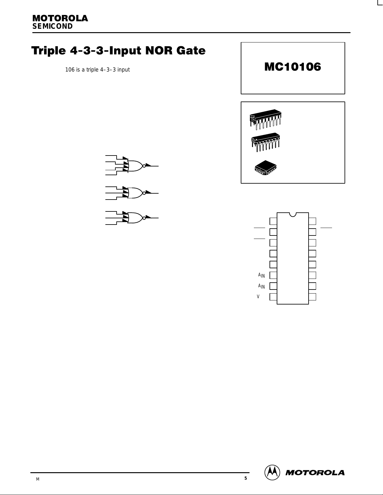
The MC10106 is a triple 4–3–3 input NOR gate.
PD= 30 mW typ/gate (No Load)
tpd= 2.0 ns typ
tr, tf= 2.0 ns typ (20%–80%)
LOGIC DIAGRAM
4
5
6
7
9
10
11
12
13
14
V
= PIN 1
CC1
V
= PIN 16
CC2
VEE= PIN 8
3
2
15
CERAMIC PACKAGE
PLASTIC PACKAGE
DIP
PIN ASSIGNMENT
V
B
OUT
A
OUT
CC1
A
IN
A
IN
A
IN
A
IN
V
EE
1
2
3
4
5
6
7
8
L SUFFIX
CASE 620–10
P SUFFIX
CASE 648–08
FN SUFFIX
PLCC
CASE 775–02
16
15
14
13
12
11
10
V
C
C
C
C
B
B
B
9
CC2
OUT
IN
IN
IN
IN
IN
IN
3/93
Motorola, Inc. 1996
3–26
Pin assignment is for Dual–in–Line Package.
For PLCC pin assignment, see the Pin Conversion
T ables on page 6–11 of the Motorola MECL Data
Book (DL122/D).
REV 5
MC10106
Under
Und
(VCC)
ELECTRICAL CHARACTERISTICS
Test Limits
Pin
Characteristic Symbol
Power Supply Drain Current I
Input Current I
Output Voltage Logic 1 V
Output Voltage Logic 0 V
Threshold Voltage Logic 1 V
Threshold Voltage Logic 0 V
Switching Times (50Ω Load) ns
Propagation Delay t
Rise Time (20 to 80%) t
Fall Time (20 to 80%) t
inH
I
inL
OH
OL
OHA
OLA
4+3–
t
4–3+
3+
3–
E
Under
Test
8 23 17 21 23 mAdc
4 425 265 265 µAdc
4 0.5 0.5 0.3 µAdc
3
2
3
2
3
2
3
2
3
3
3 1.1 3.6 1.1 2.0 3.3 1.1 3.7
3 1.1 3.6 1.1 2.0 3.3 1.1 3.7
–30°C +25°C +85°C
Min Max Min Typ Max Min Max
–1.060
–1.060
–1.890
–1.890
–1.080
–1.080
1.0
1.0
–0.890
–0.890
–1.675
–1.675
–1.655
–1.655
3.1
3.1
–0.960
–0.960
–1.850
–1.850
–0.980
–0.980
1.0
1.0
2.0
2.0
–0.810
–0.810
–1.650
–1.650
–1.630
–1.630
2.9
2.9
–0.890
–0.890
–1.825
–1.825
–0.910
–0.910
1.0
1.0
–0.700
–0.700
–1.615
–1.615
–1.595
–1.595
3.3
3.3
Unit
Vdc
Vdc
Vdc
Vdc
ELECTRICAL CHARACTERISTICS (continued)
TEST VOLTAGE VALUES (Volts)
@ Test Temperature V
–30°C –0.890 –1.890 –1.205 –1.500 –5.2
+25°C –0.810 –1.850 –1.105 –1.475 –5.2
+85°C –0.700 –1.825 –1.035 –1.440 –5.2
Pin
Characteristic Symbol
Power Supply Drain Current I
Input Current I
Output Voltage Logic 1 V
Output Voltage Logic 0 V
Threshold Voltage Logic 1 V
Threshold Voltage Logic 0 V
Switching Times (50Ω Load) Pulse In Pulse Out –3.2 V +2.0 V
Propagation Delay t
Rise Time (20 to 80%) t
Fall Time (20 to 80%) t
Each MECL 10,000 series circuit has been designed to meet the dc specifications shown in the test table, after thermal equilibrium has been
established. The circuit is in a test socket or mounted on a printed circuit board and transverse air flow greater than 500 linear fpm is maintained.
Outputs are terminated through a 50-ohm resistor to –2.0 volts. Test procedures are shown for only one gate. The other gates are tested in the
same manner.
inH
I
inL
OH
OL
OHA
OLA
4+3–
t
4–3+
3+
3–
E
Test
8 8 1, 16
4 4 8 1, 16
4 4 8 1, 16
3
2
3
2
3
2
3
2
3
3
3 4 3 8 1, 16
3 4 3 8 1, 16
IHmax
er
TEST VOLTAGE APPLIED TO PINS LISTED BELOW
V
IHmax
4
9
V
ILmin
V
ILmin
V
IHAminVILAmax
V
IHAminVILAmax
4
9
4
9
4
4
3
3
V
EE
V
EE
8
8
8
8
8
8
8
8
8
8
Gnd
1, 16
1, 16
1, 16
1, 16
1, 16
1, 16
1, 16
1, 16
1, 16
1, 16
DL122 — Rev 6
3–27 MOTOROLAMECL Data
 Loading...