

MOTOROLA MC10106FNR2 Datasheet
SEMICONDUCTOR TECHNICAL DATA
3–26
REV 5
Motorola, Inc. 1996
3/93
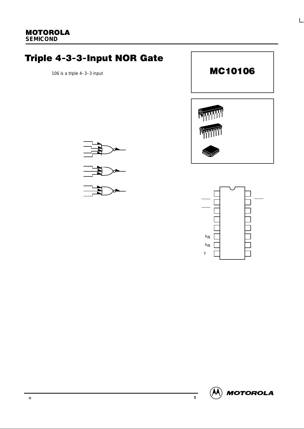
The MC10106 is a triple 4–3–3 input NOR gate.
PD= 30 mW typ/gate (No Load)
tpd= 2.0 ns typ
tr, tf= 2.0 ns typ (20%–80%)
LOGIC DIAGRAM
V
CC1
= PIN 1
V
CC2
= PIN 16
VEE= PIN 8
14
12
13
15
11
9
10
2
7
5
3
6
4
DIP
PIN ASSIGNMENT
V
CC1
B
OUT
A
OUT
A
IN
A
IN
A
IN
A
IN
V
EE
V
CC2
C
OUT
C
IN
C
IN
C
IN
B
IN
B
IN
B
IN
16
15
14
13
12
11
10
9
1
2
3
4
5
6
7
8
Pin assignment is for Dual–in–Line Package.
For PLCC pin assignment, see the Pin Conversion
T ables on page 6–11 of the Motorola MECL Data
Book (DL122/D).
L SUFFIX
CERAMIC PACKAGE
CASE 620–10
P SUFFIX
PLASTIC PACKAGE
CASE 648–08
FN SUFFIX
PLCC
CASE 775–02
MC10106
3–27 MOTOROLAMECL Data
DL122 — Rev 6
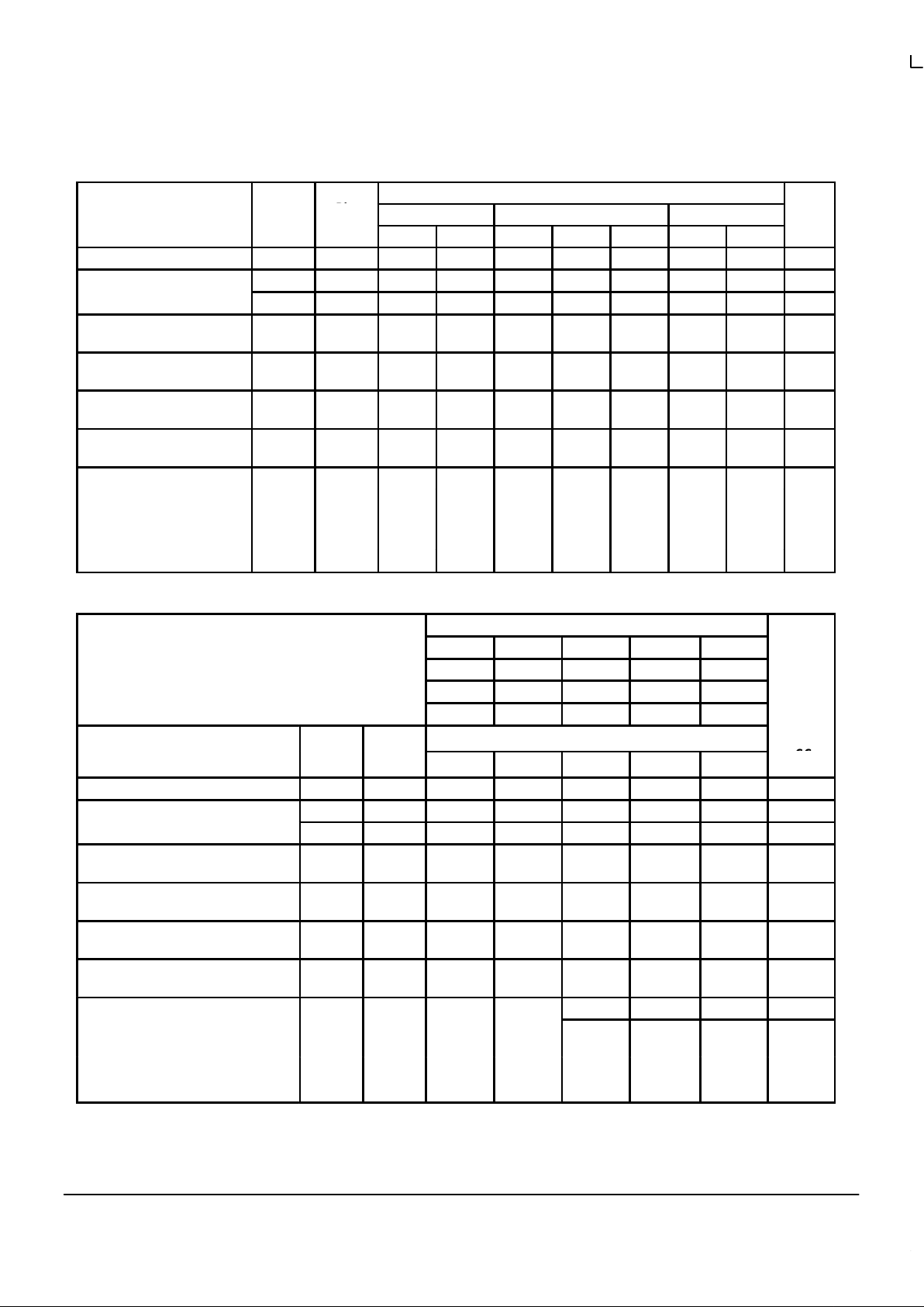
ELECTRICAL CHARACTERISTICS
Test Limits
Pin
Under
–30°C +25°C +85°C
Characteristic Symbol
Under
Test
Min Max Min Typ Max Min Max
Unit
Power Supply Drain Current I
E
8 23 17 21 23 mAdc
Input Current I
inH
4 425 265 265 µAdc
I
inL
4 0.5 0.5 0.3 µAdc
Output Voltage Logic 1 V
OH
3
2
–1.060
–1.060
–0.890
–0.890
–0.960
–0.960
–0.810
–0.810
–0.890
–0.890
–0.700
–0.700
Vdc
Output Voltage Logic 0 V
OL
3
2
–1.890
–1.890
–1.675
–1.675
–1.850
–1.850
–1.650
–1.650
–1.825
–1.825
–1.615
–1.615
Vdc
Threshold Voltage Logic 1 V
OHA
3
2
–1.080
–1.080
–0.980
–0.980
–0.910
–0.910
Vdc
Threshold Voltage Logic 0 V
OLA
3
2
–1.655
–1.655
–1.630
–1.630
–1.595
–1.595
Vdc
Switching Times (50Ω Load) ns
Propagation Delay t
4+3–
t
4–3+
3
3
1.0
1.0
3.1
3.1
1.0
1.0
2.0
2.0
2.9
2.9
1.0
1.0
3.3
3.3
Rise Time (20 to 80%) t
3+
3 1.1 3.6 1.1 2.0 3.3 1.1 3.7
Fall Time (20 to 80%) t
3–
3 1.1 3.6 1.1 2.0 3.3 1.1 3.7
ELECTRICAL CHARACTERISTICS (continued)
TEST VOLTAGE VALUES (Volts)
@ Test Temperature V
IHmax
V
ILmin
V
IHAminVILAmax
V
EE
–30°C –0.890 –1.890 –1.205 –1.500 –5.2
+25°C –0.810 –1.850 –1.105 –1.475 –5.2
+85°C –0.700 –1.825 –1.035 –1.440 –5.2
Pin
TEST VOLTAGE APPLIED TO PINS LISTED BELOW
Characteristic Symbol
Und
er
Test
V
IHmax
V
ILmin
V
IHAminVILAmax
V
EE
(VCC)
Gnd
Power Supply Drain Current I
E
8 8 1, 16
Input Current I
inH
4 4 8 1, 16
I
inL
4 4 8 1, 16
Output Voltage Logic 1 V
OH
3
2
8
8
1, 16
1, 16
Output Voltage Logic 0 V
OL
3
2
4
9
8
8
1, 16
1, 16
Threshold Voltage Logic 1 V
OHA
3
2
4
9
8
8
1, 16
1, 16
Threshold Voltage Logic 0 V
OLA
3
2
4
9
8
8
1, 16
1, 16
Switching Times (50Ω Load) Pulse In Pulse Out –3.2 V +2.0 V
Propagation Delay t
4+3–
t
4–3+
3
3
4
4
3
3
8
8
1, 16
1, 16
Rise Time (20 to 80%) t
3+
3 4 3 8 1, 16
Fall Time (20 to 80%) t
3–
3 4 3 8 1, 16
Each MECL 10,000 series circuit has been designed to meet the dc specifications shown in the test table, after thermal equilibrium has been
established. The circuit is in a test socket or mounted on a printed circuit board and transverse air flow greater than 500 linear fpm is maintained.
Outputs are terminated through a 50-ohm resistor to –2.0 volts. Test procedures are shown for only one gate. The other gates are tested in the
same manner.
 Loading...