

Motorola MBR0540T1 Datasheet
SEMICONDUCTOR TECHNICAL DATA
SOD–123 Power Surface Mount Package
The Schottky Power Rectifier employs the Schottky Barrier principle with a barrier
metal that produces optimal forward voltage drop–reverse current tradeoff. Ideally
suited for low voltage, high frequency rectification, or as a free wheeling and polarity
protection diodes in surface mount applications where compact size and weight are
critical to the system. This package provides an alternative to the leadless 34 MELF
style package. These state–of–the–art devices have the following features:
• Guardring for Stress Protection
• Very Low Forward Voltage
• Epoxy Meets UL94, VO at 1/8″
• Package Designed for Optimal Automated Board Assembly
Mechanical Characteristics:
• Reel Options: 3,000 per 7 inch reel / 8 mm tape
• Reel Options: 10,000 per 13 inch reel / 8 mm tape
• Device Marking: B4
• Polarity Designator: Cathode Band
• Weight: 11.7 mg (approximately)
• Case: Epoxy Molded
• Finish: All External Surfaces Corrosion Resistant and Terminal Leads are Readily Solderable
• Lead and Mounting Surface Temperature for Soldering Purposes: 260°C max. for 10 Seconds
MAXIMUM RATINGS
Rating Symbol Value Unit
Peak Repetitive Reverse Voltage
Working Peak Reverse Voltage
DC Blocking Voltage
Average Rectified Forward Current (At Rated VR, TC = 115°C) I
Peak Repetitive Forward Current
(At Rated VR, Square Wave, 20 kHz, TC = 115°C)
Non–Repetitive Peak Surge Current
(Surge applied at rated load conditions, halfwave, single phase, 60 Hz)
Storage / Operating Case Temperature T
Operating Junction Temperature T
Voltage Rate of Change (Rated VR, TJ = 25°C) dv/dt 1,000
V
RRM
V
RWM
I
FRM
I
FSM
stg
V
R
O
, T
C
J
THERMAL CHARACTERISTICS
Thermal Resistance – Junction–to–Lead (2)
Thermal Resistance – Junction–to–Ambient (3)
R
tjl
R
tja
ELECTRICAL CHARACTERISTICS
Maximum Instantaneous Forward Voltage (1)
(IF = 0.5 A)
(IF = 1 A)
Maximum Instantaneous Reverse Current
(VR = 40 V)
(VR = 20 V)
This document contains information on a new product. Specifications and information herein are subject to change without notice.
(1) Pulse Test: Pulse Width ≤ 250 µs, Duty Cycle ≤ 2.0%.
(2) Mounted with minimum recommended pad size, PC Board FR4.
(3) 1 inch square pad size (1 X 0.5 inch for each lead) on FR4 board.
Rev 2
V
F
I
R
SCHOTTKY BARRIER
–55 to 150 °C
–55 to 150 °C
TJ = 25°C TJ = 100°C
0.51
0.62
TJ = 25°C TJ = 100°C
20
10
Order this document
by MBR0540T1/D
RECTIFIER
0.5 AMPERES
40 VOLTS
CASE 425–04, Style 1
SOD–123
40 V
0.5 A
1.0 A
5.5 A
118
206
0.46
0.61
5,000
13,000
V/ms
°C/W
V
m
A
Rectifier Device Data
Motorola, Inc. 1996
1
MBR0540T1
10
25°C
100
10
1.0
0.1
, INSTANTANEOUS FORWARD CURRENT (AMPS)I
F
I
0.2
100E–3
10E–3
1.0E–3
100E–6
10E–6
, REVERSE CURRENT (AMPS)
1.0E–6
R
100E–9
1.0
TJ = 125°C
VF, INSTANTANEOUS FORWARD VOLTAGE (VOLTS)
TJ = –40°C
TJ = 25°C
TJ = 100°C
0.6 1.20.4 0.8
1.0
TJ = 125°C
TJ = 100°C
0.1
, INSTANTANEOUS FORWARD CURRENT (AMPS)
F
0.2
VF, MAXIMUM INSTANTANEOUS FORWARD VOLTAGE (VOLTS)
TJ = 25°C
0.6 1.20.4 0.8 1.0
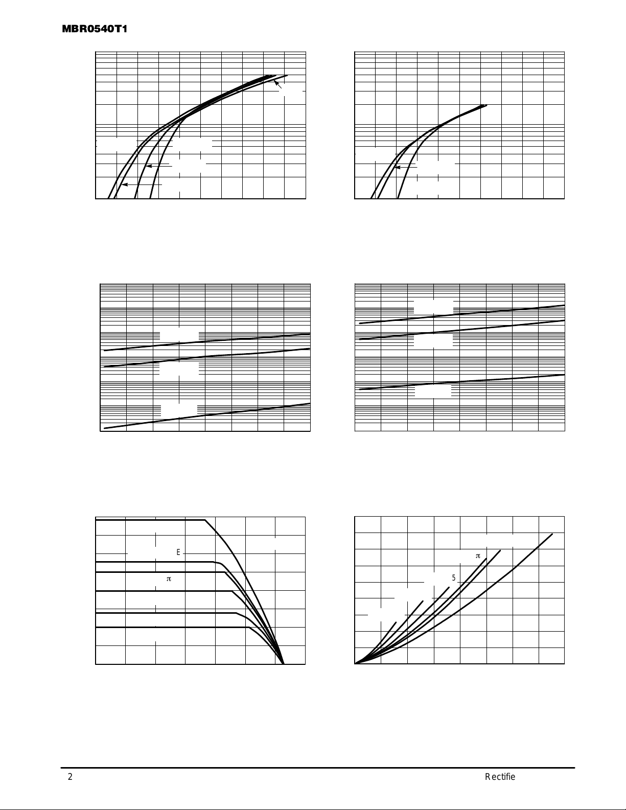
Figure 1. T ypical Forward Voltage Figure 2. Maximum Forward V oltage
100E–3
TJ = 125°C
TJ = 100°C
TJ = 25°C
10 20 30
VR, REVERSE VOLTAGE (VOLTS)
VR, REVERSE VOLTAGE (VOLTS)
TJ = 125°C
TJ = 100°C
TJ = 25°C
10 20 30
VR, REVERSE VOLTAGE (VOLTS)
400
10E–3
1.0E–3
100E–6
10E–6
1.0E–6
, MAXIMUM REVERSE CURRENT (AMPS)
R
I
100E–9
400
Figure 3. T ypical Reverse Current Figure 4. Maximum Reverse Current
, AVERAGE POWER DISSIPATION (WA TTS) I
P
0.45
0.40
0.35
0.30
0.25
0.20
0.15
0.10
0.05
FO
0
SQUARE WAVE
Ipk/Io =
p
Ipk/Io = 5
Ipk/Io = 10
Ipk/Io = 20
0.10
0.2 0.3 0.5 0.8
IO, AVERAGE FORW ARD CURRENT (AMPS)
0.440
dc
0.6 0.7
0.8
0.7
0.6
0.5
0.4
0.3
0.2
0.1
, AVERAGE FORW ARD CURRENT (AMPS)I
O
0
dc
SQUARE WAVE
Ipk/Io =
p
Ipk/Io = 5
Ipk/Io = 10
Ipk/Io = 20
20 600
TL, LEAD TEMPERATURE (
80 120100
°
C)
FREQ = 20 kHz
140
Figure 5. Current Derating Figure 6. Forward Power Dissipation
2
Rectifier Device Data
 Loading...