

MAX809, MAX810
3-Pin Micropr ocessor
Reset Monitors
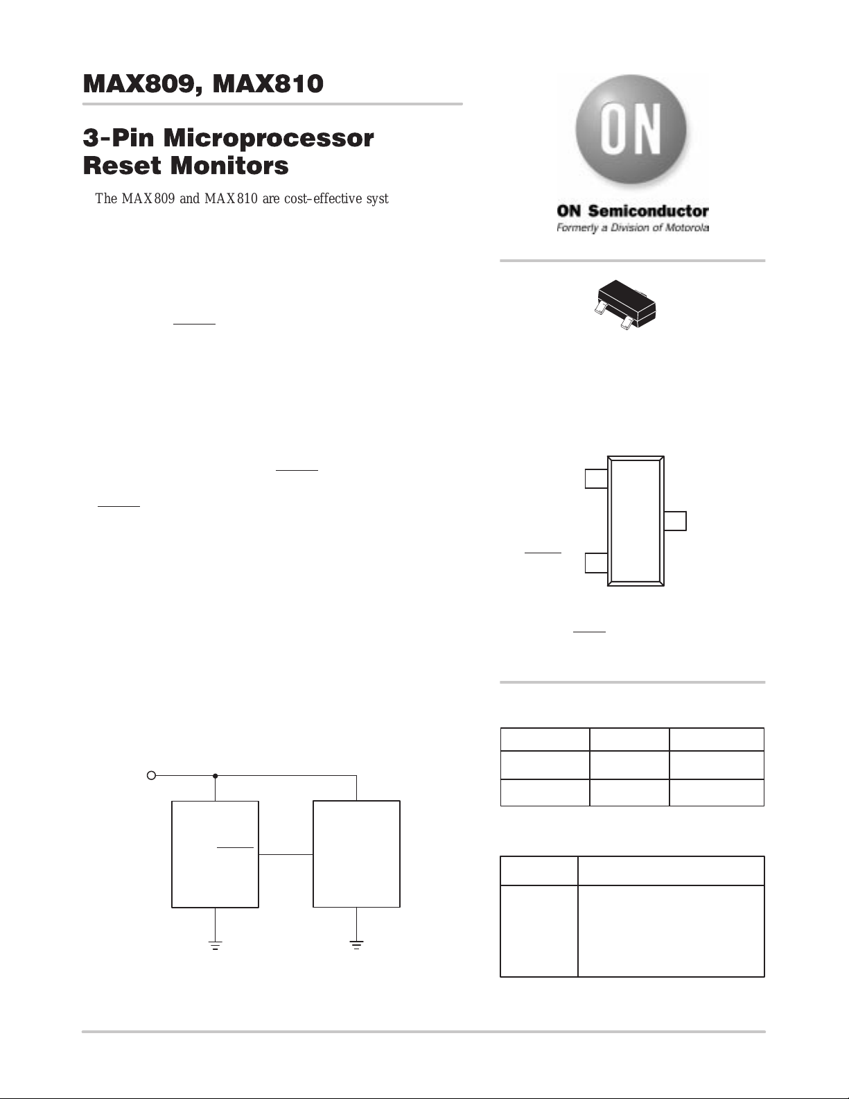
The MAX809 and MAX810 are cost–effective system supervisor
circuits designed to monitor VCC in digital systems and provide a reset
signal to the host processor when necessary. No external components
are required.
The reset output is driven active within 20 µsec of V
through the reset voltage threshold. Reset is maintained active for a
minimum of 140msec after V
rises above the reset threshold. The
CC
MAX810 has an active–high RESET output while the MAX809 has
an active–low RESET output. The output of the MAX809 is
guaranteed valid down to VCC = 1V. Both devices are available in a
SOT–23 package.
The MAX809/810 are optimized to reject fast transient glitches on
the V
line. Low supply current of 17µA (V
CC
= 3.3V) makes these
CC
devices suitable for battery powered applications.
Features
• Precision V
Monitor for 3.0V, 3.3V, and 5.0V Supplies
CC
• 140msec Guaranteed Minimum RESET , RESET
Output Duration
• RESET Output Guaranteed to V
= 1.0V (MAX809)
CC
• Low 17µA Supply Current
• V
Transient Immunity
CC
• Small SOT–23 Package
• No External Components
• Wide Operating Temperature: –40°C to 85°C
Typical Applications
• Computers
• Embedded Systems
• Battery Powered Equipment
• Critical µP Power Supply Monitoring
falling
CC
http://onsemi.com
SOT–23
(TO–236)
CASE 318
PIN CONFIGURATION
(Top View)
1
GND
V
3
CC
RESET
(RESET)**
NOTE: *SOT–23 is equivalent to JEDEC (TO–236)
2
SOT–23*
** RESET
** RESET is for MAX810
ORDERING INFORMATION
is for MAX809
TYPICAL APPLICATION DIAGRAM
V
CC
V
CC
MAX809
RESET
GND GND
Semiconductor Components Industries, LLC, 1999
February , 2000 – Rev. 2
V
CC
PROCESSOR
RESET
INPUT
Device Package Shipping
MAX809xTR SOT–23 3000 Tape/Reel
MAX810xTR SOT–23 3000 Tape/Reel
NOTE: The ”x” denotes a suffix for VCC threshold –
see table below
Suffix Reset VCC Threshold (V)
L 4.63
M 4.38
J* 4.00
T 3.08
S 2.93
R 2.63
NOTE: *J version is available for MAX809 only
1 Publication Order Number:
MAX809/D
MAX809, MAX810
ABSOLUTE MAXIMUM RATINGS*
Symbol Parameter Value Unit
Supply Voltage (VCC to GND) 6.0 V
RESET, RESET –0.3 to (VCC + 0.3) V
Input Current, V
Output Current, RESET, RESET 20 mA
dV/dt (VCC) 100 V/µsec
P
D
T
A
T
stg
T
sol
* Maximum Ratings are those values beyond which damage to the device may occur.
Power Dissipation (TA ≤ 70°C)
SOT–23 (derate 4mW/°C above +70°C)
Operating Temperature Range –40 to +85 °C
Storage Temperature Range –65 to +150 °C
Lead Temperature (Soldering, 10 Seconds) +260 °C
CC
20 mA
230
mW
http://onsemi.com
2
MAX809, MAX810
ББББББ
Á
ББББББ
Á
Á
Á
ББББББ
ББББББ
ELECTRICAL CHARACTERISTICS (VCC = Full Range, TA = –40°C to +85°C unless otherwise noted. typical values are at T
= 1.2mA
= 3.2mA
= 500µA
= 800µA
= 1.2mA
= 3.2mA
(Note NO TAG)
1.0
1.2
—
—
4.56
4.50
4.31
4.25
3.93
3.89
3.04
3.00
2.89
2.85
2.59
2.55
—
—
—
0.8 V
CC
VCC – 1.5
—
—
0.8 V
CC
—
—
24
17
4.63
—
4.38
—
4.00
—
3.08
—
2.93
—
2.63
—
—
—
—
—
—
—
—
— —
5.5
5.5
µA
60
50
4.70
4.75
4.45
4.50
4.06
4.10
3.11
3.15
2.96
3.00
2.66
2.70
0.3
0.4
0.3
—
—
0.3
0.4
= +25C, VCC = 5V for L/M/J, 3.3V for T/S, 3.0V for R)
Symbol
VCC Range
TA = 0°C to +70°C
TA = –40°C to +85°C
I
CC
Supply Current
MAX8xxL/M/J: VCC < 5.5V
MAX8xxR/S/T: VCC < 3.6V
V
TH
Reset Threshold (Note NO TAG)
MAX8xxL: TA = 25°C
TA = –40°C to +85°C
MAX8xxM: TA = 25°C
TA = –40°C to +85°C
MAX809J: TA = 25°C
TA = –40°C to +85°C
MAX8xxT: TA = 25°C
TA = –40°C to +85°C
MAX8xxS: TA = 25°C
TA = –40°C to +85°C
MAX8xxR: TA = 25°C
TA = –40°C to +85°C
Reset Threshold Temperature Coefficient — 30 — ppm/°C
VCC to Reset Delay VCC = VTH to (VTH – 100mV) — 20 — µsec
Reset Active Timeout Period 140 240 560 msec
V
OL
RESET Output Voltage Low (MAX809)
MAX809R/S/T: VCC = VTH min, I
MAX809L/M/J: VCC = VTH min, I
VCC > 1.0V, I
V
OH
RESET Output Voltage High (MAX809)
MAX809R/S/T: VCC > VTH max, I
SINK
= 50µA
MAX809L/M/J: VCC > VTH max, I
V
OL
RESET Output Voltage Low (MAX810)
MAX810R/S/T: VCC = VTH max, I
MAX810L/M/J: VCC = VTH max, I
V
OH
RESET Output Voltage High (MAX810)
1.8 < VCC < VTH min, I
1. Production testing done at TA = 25°C, over temperature limits guaranteed by design.
Characteristic Min Typ Max Unit
SINK
SINK
SOURCE
SOURCE
SINK
SINK
SOURCE
= 150µA
A
V
V
V
V
V
V
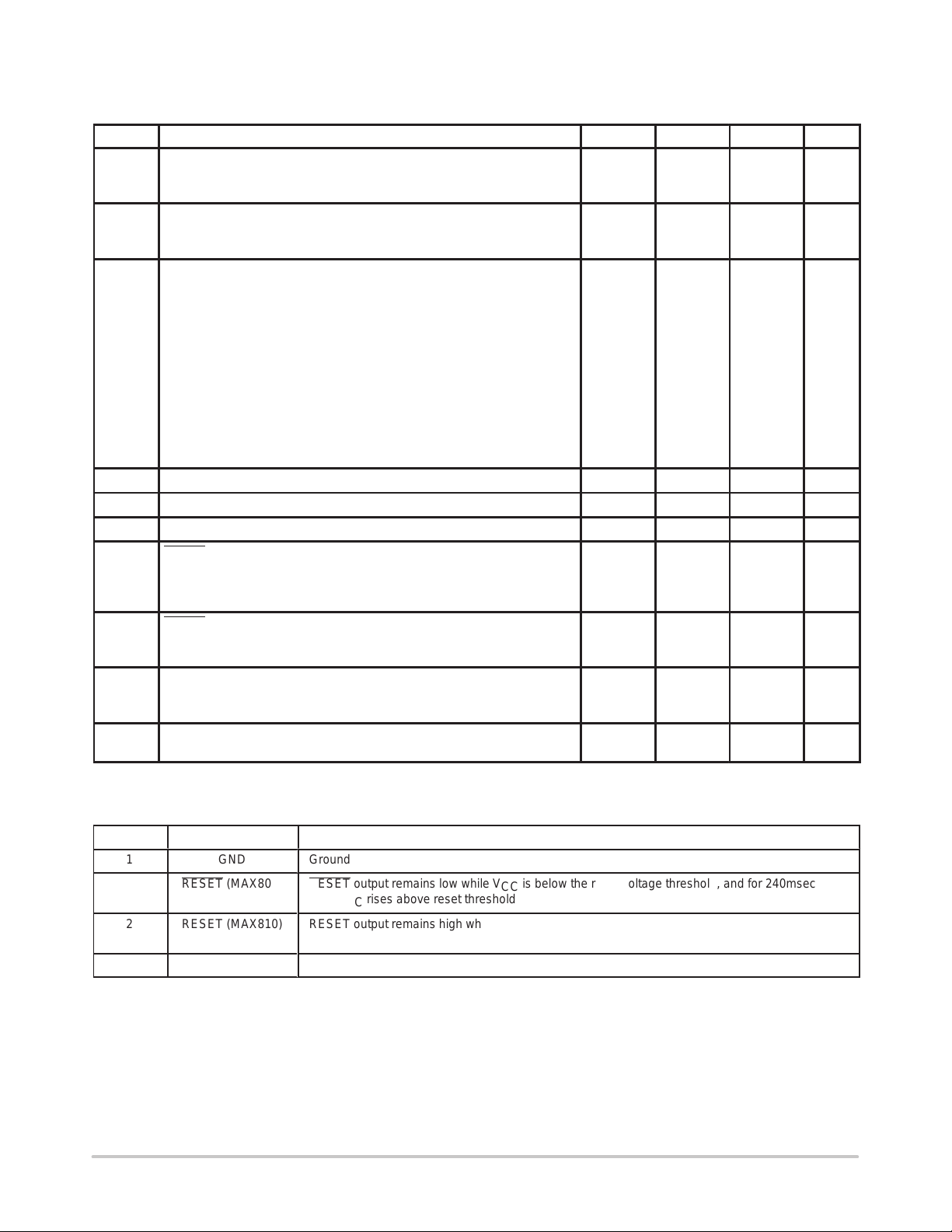
PIN DESCRIPTION
Pin No. Symbol Description
1
2
ÁÁÁ
2
3
GND
RESET (MAX809)
ÁÁÁÁ
RESET (MAX810)
V
CC
Ground
RESET output remains low while VCC is below the reset voltage threshold, and for 240msec (typ.)
after VCC rises above reset threshold
ББББББББББББББББББББББ
RESET output remains high while VCC is below the reset voltage threshold, and for 240msec (typ.)
after VCC rises above reset threshold
Supply Voltage (typ.)
http://onsemi.com
3

MAX809, MAX810
APPLICATIONS INFORMATION
VCC Transient Rejection
The MAX809/810 provides accurate V
monitoring and
CC
reset timing during power–up, power–down, and
brownout/sag conditions, and rejects negative–going
transients (glitches) on the power supply line. Figure 1
shows the maximum transient duration vs. maximum
negative excursion (overdrive) for glitch rejection. Any
combination of duration and overdrive which lies under the
curve will not generate a reset signal. Combinations above
the curve are detected as a brownout or power–down.
Transient immunity can be improved by adding a capacitor
in close proximity to the V
V
CC
400
TA = +25° C
m
320
240
160
90
MAX8xxR/S/T
0
1 10 100 1000
MAXIMUM TRANSIENT DURATION ( sec)
RESET COMPARATOR OVERDRIVE,
Figure 1. Maximum Transient Duration vs. Overdrive
for Glitch Rejection at 25° C
RESET Signal Integrity During Power–Down
pin of the MAX809/810.
CC
V
TH
Overdrive
Duration
MAX8xxL/M/J
(VTH – VCC (mV)
The MAX809 RESET output is valid to VCC = 1.0V.
Below this voltage the output becomes an ”open circuit” and
does not sink current. This means CMOS logic inputs to the
µP will be floating at an undetermined voltage. Most digital
systems are completely shutdown well above this voltage.
However, in situations where RESET
must be maintained
valid to VCC = 0V, a pull–down resistor must be connected
from RESET
to ground to discharge stray capacitances and
hold the output low (Figure 2). This resistor value, though
not critical, should be chosen such that it does not
appreciably load RESET
under normal operation (100k
W
will be suitable for most applications). Similarly, a pull–up
resistor to V
is required for the MAX810 to ensure a valid
CC
high RESET for VCC below 1.0V.
V
CC
V
CC
MAX809
RESET
GND
R1
100 k
Figure 2. Ensuring RESET Valid to VCC = 0 V
Processors With Bidirectional I/O Pins
Some µP’s (such as Motorola 68HC11) have
bi–directional reset pins. Depending on the current drive
capability of the processor pin, an indeterminate logic level
may result if there is a logic conflict. This can be avoided
by adding a 4.7kW resistor in series with the output of the
MAX809/810 (Figure 3). If there are other components in
the system which require a reset signal, they should be
buffered so as not to load the reset line. If the other
components are required to follow the reset I/O of the µP , the
buffer should be connected as shown with the solid line.
BUFFER
V
CC
V
CC
MAX809
RESET
GND GND
47 k
RESET
Figure 3. Interfacing to Bidirectional Reset I/O
BUFFERED RESET
TO OTHER SYSTEM
COMPONENTS
V
CC
m
P
http://onsemi.com
4

MAX809, MAX810
35
30
P
–UP
S
U
)
TYPICAL CHARACTERISTICS
30
m
25
20
15
10
SUPPLY CURRENT ( A)
5
0
–40 –20 0 20 40 60 85
TEMPERATURE (C°)
Figure 4. Supply Current vs Temperature
(No Load, MAX8xxR/S/T)
100
m
80
60
40
20
POWER–DOWN RESET DELAY ( sec)
0
–40 –20 0 20 40 60 85
VOD = 200 mV
TEMPERATURE (C°)
VOD = VTH – V
Figure 6. Power–Down Reset Delay vs
T emperature and Overdrive (MAX8xxR/S/T)
VCC = 5 V
VCC = 3 V
VCC = 1 V
VOD = 10 mV
VOD = 10 mV
VOD = 100 mV
CC
25
m
20
15
10
SUPPLY CURRENT ( A)
5
0
–40 –20 0 20 40 60 85
TEMPERATURE (C°)
Figure 5. Supply Current vs Temperature
(No Load, MAX8xxL/M/J/)
140
120
m
100
80
60
40
20
POWER–DOWN RESET DELAY ( sec)
0
–40 –20 0 20 40 60 85
VOD = 200 mV
TEMPERATURE (C°)
Figure 7. Power–Down Reset Delay vs
T emperature and Overdrive (MAX8xxL/M/J)
VCC = 5 V
VCC = 3 V
VCC = 1 V
VOD = VTH – V
VOD = 10 mV
VOD = 20 mV
VOD = 100 mV
CC
250
245
T (msec
240
ET TIMEO
235
RE
230
OWER
225
–40 –20 0 20 40 60 85
TEMPERATURE (C°)
MAX8xxL/M/J
MAX8xxR/S/T
Figure 8. Power–Up Reset Timeout vs
T emperature
1.003
1.002
1.001
1.000
0.999
NORMALIZED THRESHOLD
0.998
0.997
http://onsemi.com
5
–40 –20 0 20 40 85
TEMPERATURE (C°)
60
Figure 9. Normalized Reset Threshold vs
T emperature

TAPING FORM
БББББББББББ
БББББББББББ
БББББББББББ
БББББББББББ
БББББББББББ
БББББББББББ
БББББББББББ
БББББББББББ
БББББББББББ
БББББББББББ
БББББББББББ
MAX809, MAX810
Component Taping Orientation for 3L SOT–23 (JEDEC–236) Devices
USER DIRECTION OF FEED
DEVICE
MARKING
PIN 1
Standard Reel Component Orientation
(Mark Right Side Up)
Tape & Reel Specifications Table
Package Carrier Width (W) Pitch (P) Part Per Full Reel Reel Size
SOT–23
8 mm 4 mm 3000 7 inches
MARKING DIAGRAM
SOT–23
xxYW
YW = Date Code
MARKING
ON Semiconductor Part # Reset Threshold or Address Marking
MAX809L
MAX809M
MAX809T
MAX809S
MAX809R
MAX809J
MAX810L
MAX810M
MAX810T
MAX810S
MAX810R
YW = Date code
4.63
4.38
3.08
2.93
2.63
4.00
4.63
4.38
3.08
2.93
2.63
J1YW
J2YW
J3YW
J4YW
J5YW
J6YW
K1YW
K2YW
K3YW
K4YW
K5YW
http://onsemi.com
6

MAX809, MAX810
P ACKAGE DIMENSIONS
SOT–23
PLASTIC PACKAGE (TO–236)
CASE 318–08
ISSUE AF
NOTES:
1. DIMENSIONING AND TOLERANCING PER ANSI
Y14.5M, 1982.
2. CONTROLLING DIMENSION: INCH.
A
L
3
1
2
S
B
GV
C
D
H
K
J
3. MAXIMUM LEAD THICKNESS INCLUDES LEAD
FINISH THICKNESS. MINIMUM LEAD THICKNESS
IS THE MINIMUM THICKNESS OF BASE
MATERIAL.
INCHES
DIMAMIN MAX MIN MAX
0.1102 0.1197 2.80 3.04
B 0.0472 0.0551 1.20 1.40
C 0.0350 0.0440 0.89 1.11
D 0.0150 0.0200 0.37 0.50
G 0.0701 0.0807 1.78 2.04
H 0.0005 0.0040 0.013 0.100
J 0.0034 0.0070 0.085 0.177
K 0.0140 0.0285 0.35 0.69
L 0.0350 0.0401 0.89 1.02
S 0.0830 0.1039 2.10 2.64
V 0.0177 0.0236 0.45 0.60
MILLIMETERS
http://onsemi.com
7

MAX809, MAX810
ON Semiconductor and are trademarks of Semiconductor Components Industries, LLC (SCILLC). SCILLC reserves the right to make changes
without further notice to any products herein. SCILLC makes no warranty , representation or guarantee regarding the suitability of its products for any particular
purpose, nor does SCILLC assume any liability arising out of the application or use of any product or circuit, and specifically disclaims any and all liability ,
including without limitation special, consequential or incidental damages. “Typical” parameters which may be provided in SCILLC data sheets and/or
specifications can and do vary in different applications and actual performance may vary over time. All operating parameters, including “Typicals” must be
validated for each customer application by customer’s technical experts. SCILLC does not convey any license under its patent rights nor the rights of others.
SCILLC products are not designed, intended, or authorized for use as components in systems intended for surgical implant into the body, or other applications
intended to support or sustain life, or for any other application in which the failure of the SCILLC product could create a situation where personal injury or
death may occur. Should Buyer purchase or use SCILLC products for any such unintended or unauthorized application, Buyer shall indemnify and hold
SCILLC and its officers, employees, subsidiaries, affiliates, and distributors harmless against all claims, costs, damages, and expenses, and reasonable
attorney fees arising out of, directly or indirectly , any claim of personal injury or death associated with such unintended or unauthorized use, even if such claim
alleges that SCILLC was negligent regarding the design or manufacture of the part. SCILLC is an Equal Opportunity/Affirmative Action Employer .
PUBLICATION ORDERING INFORMATION
NORTH AMERICA Literature Fulfillment:
Literature Distribution Center for ON Semiconductor
P.O. Box 5163, Denver, Colorado 80217 USA
Phone: 303–675–2175 or 800–344–3860 Toll Free USA/Canada
Fax: 303–675–2176 or 800–344–3867 Toll Free USA/Canada
Email: ONlit@hibbertco.com
Fax Response Line: 303–675–2167 or 800–344–3810 T oll Free USA/Canada
N. American Technical Support: 800–282–9855 Toll Free USA/Canada
EUROPE: LDC for ON Semiconductor – European Support
German Phone: (+1) 303–308–7140 (M–F 1:00pm to 5:00pm Munich Time)
Email: ONlit–german@hibbertco.com
French Phone: (+1) 303–308–7141 (M–F 1:00pm to 5:00pm Toulouse T ime)
Email: ONlit–french@hibbertco.com
English Phone: (+1) 303–308–7142 (M–F 12:00pm to 5:00pm UK Time)
Email: ONlit@hibbertco.com
EUROPEAN TOLL–FREE ACCESS*: 00–800–4422–3781
*Available from Germany, France, Italy, England, Ireland
CENTRAL/SOUTH AMERICA:
Spanish Phone: 303–308–7143 (Mon–Fri 8:00am to 5:00pm MST)
Email: ONlit–spanish@hibbertco.com
ASIA/PACIFIC : LDC for ON Semiconductor – Asia Support
Phone: 303–675–2121 (Tue–Fri 9:00am to 1:00pm, Hong Kong Time)
T oll Free from Hong Kong & Singapore:
001–800–4422–3781
Email: ONlit–asia@hibbertco.com
JAPAN: ON Semiconductor, Japan Customer Focus Center
4–32–1 Nishi–Gotanda, Shinagawa–ku, T okyo, Japan 141–8549
Phone: 81–3–5740–2745
Email: r14525@onsemi.com
ON Semiconductor Website: http://onsemi.com
For additional information, please contact your local
Sales Representative.
http://onsemi.com
8
MAX809/D
 Loading...