

Page 1

CPX8000 Series CPX8216/CPX8216T
®
CompactPCI
System
Reference Manual
CPX8216A/RM4
August 2002 Edition
Page 2

© Copyright 2002 Motorola Inc.
All rights reserved.
Printed in the United States of America.
Motorola® and the Motorola symbol are registered trademarks of Motorola, Inc.
PowerPC® and the PowerPC logo are registered trade mark s of International Business
Machines Corporation (IBM) and are used by Motorola, Inc. under license from IBM.
CompactPCI® is a registered trademark o f the PC I In dustrial Computer Manufacturer’s
Group (PICMG).
All other product or service names mentioned in this doc ument are trademarks or registered
trademarks of their respective holders.
Page 3

Safety Summary
Warning
The followi ng gen eral safety precaut io ns mus t be observed during all ph ases of oper ation, service, an d repa ir of
this equipment. Failure to comply with these precautions or with specific warnings elsewhere in this manual
could result in personal injury or damage to the equipment.
The safety precautions listed below represent warnings of certain dangers of which Motorola is aware. You, as
the user of the product, should follow these warnings and all other safety precautions necessary for the safe
operation of the equipment in your operating environment.
Ground the Instrument.
T o minimi ze shock haz ard, the equi pment chassis and enclosure must be connec ted to an electr ical ground . If the
equipment is supp lied with a three-co nduct or AC power cable, th e powe r cabl e mus t be plu gged int o an approv ed
three-con tact e lectrical outlet, with the groundin g wir e (green/yellow) r eliab ly co nnected to an electrical ground
(safety ground) at the power outlet. The power jack and mating plug of the power cable meet International
Electrotechnical Commission (IEC) safety standards and local electrical regulatory codes.
Do Not Operate in an Explosive Atmosphere.
Do not operate the equipm ent in a ny explosive atm osp here such as in the presence of flam mabl e g ases or fumes.
Operation of any electrical equipment in such an environment could result in an explosion and cause injury or
damage.
Keep Away From Live Circuits Inside the Equipment.
Operating personnel must not remove equipment covers. Only Factory Authorized Service Personnel or other
qualified service personnel may remove equipment covers for internal subassembly or component replacement
or any inte rnal adjus tment. Se rvice pe rsonnel s houl d not repl ace comp onents w ith power cab le co nnected . Under
certain conditions, dangerous voltages may exist even with the power cable removed. To avoid injuries, such
personnel should always disconnect power and discharge circuits before touching components.
Use Caution When Exposing or Handling a CRT.
Breakage of a Cathode-Ray Tube (CRT) causes a high-velocity scattering of glass fragments (implosion). To
prevent CRT implo sion , do not ha ndl e the CRT and avo id roug h handling or jarrin g of t he equ ipm ent . Ha ndling
of a CRT should be done only by qualified service personnel using approved safety mask and gloves.
Do Not Substitute Parts or Modify Equipment.
Do not install substitute parts or perform any unauthorized modification of the equipment. Contact your local
Motorola representative for service and repair to ensure that all safety features are maintained.
Observe Warnings in Manual.
Warnings, such as the example below, precede potentially dangerous procedures throughout this manual.
Instructions contained in the warnings must be followed. You should also employ all other safety precautions
which you deem necessary for the operation of the equipment in your operating environment.
Warnin g
To prevent serious injury or death from dangerous voltages, use extreme
caution when handling, testing, and adjusting this equipment and its
components.
Page 4

Flammability
!
Warning
All Motorola PWBs (printed wiring boards) are manufactured with a flammability rating
of 94V-0 by UL-recognized manufac turers.
CE Notice (European Community)
Warnin g
Motorola Computer Group p roducts with t he CE marking comply wi th the EMC Dir ective
(89/336/EEC). Compliance with this dir ective implies conformity to the following
European Norms:
EN55022 “Limits and Methods of Measurement of Radio Interference Characteristics
of Information Technology Equipment”; this product tested to Equipment Class A
EN55024 “Information technol ogy equipment—Immunity characteristics—Limits and
methods of measurement”
This product also fulfill s EN60950 (pr oduct safety) which is essentially the requir ement fo r
the Low Voltage Directive (73/23/EEC).
AC configurations of this system also mee t the req uirements of the following European
standards:
EN61000-3-2 “Limits of Harmonic Current Emissions (equipment input current ≤ 16
A per phase)”
This is a Class A product. In a domestic environment, this product may
cause radio interference, in which case the user may be required to take
adequate measures.
EN61000-3-3 “Limits of Voltage Fluctuations and Flicker in Low-Voltage Supply
Systems for Equipment with Rated Current ≤ 16 A”
In accordance with European Community directives, a “Declaration of Conformit y” has
been made and is available on request. Please contac t your sales representative.
This product is not a workstation per the Europe an Ergonomic Standard.
Kein Bildschirmarbeitsplatz nach dem Europäischen Ergonomie Standard.
Page 5

FCC Class A
!
Caution
This equipment ha s been tested and found to comply with the limits for a Class A digital
device, pursuant to Part 15 of the FCC Rules. These lim its are designed to provide
reasonable protec tion against harmful interferen ce when the equipment is operated in a
commercial environm ent. Thi s equipment g enerates , uses, and can rad iate radio f requency
energy and, if not ins talle d and used in accordance with the instr uction manual, may cause
harmful interference to radio communications. Operati on of this equipment in a residential
area is likely to cause ha rmful interference in which case the use r will be required to c orrect
the interference at his own expense.
Changes or modifications no t expre ssly approve d by Motor ola Computer Group could voi d
the user’s author ity to operate the equipment.
Use only shielded cables when connecting peripherals to assure that appropriate radio
frequency emissions co mpli ance is maintained.
EMI Caution
Caution
This equipment generates, uses and can radiate electromagnetic energy. It
may cause or be susceptible to electromagnetic interference (EMI) if not
installed and used with adequ at e EMI protection.
Notice
While reasonable ef forts have been made to assure the accuracy of this document,
Motorola, Inc. assumes no liabil ity re sult ing from any o missions i n thi s document, or f rom
the use of the information obtained therein. Motorola reserves the right to revise this
document and to make ch ang es from time to time in the content hereof without obligation
of Motorola to notify any person of such revision or changes.
Electronic versi ons of this material may be read online, downloaded for personal use, or
referenced in another document as a UR L to the Motorola Compute r Group Web site. The
text itself may not be published commercially in prin t or electr onic form, e dited, transla ted,
or otherwise altered without the permission of Motorola, Inc.
It is possible that this publication may con tain reference to or information about Motorola
products (mach ines and pro grams), p rogramming, or s ervi ces tha t ar e not avail able in your
Page 6

country. Such references or inform at ion must not be construed to mean that Motorola
intends to announce such Motorola produc ts, programming, or services in your country.
Limited and Restricted Rights Legend
If the documentation containe d here in is supplied, directly or indirectly, to the U.S.
Government, the following notice shall apply unless otherwise agreed to in writing by
Motoro la , Inc.
Use, duplication, or disclosure by the Government is subject to restrictions as set forth in
subparagraph (b)(3) of the Rights in Technical Data clause at DFARS 252.227-7013 (Nov.
1995) and of the Rights in Nonc ommercial Compute r Software a nd Documenta tion clause
at DF ARS 252.227-7014 (Jun. 1995).
Motoro la , Inc.
Computer Group
2900 South Diablo Way
T empe, Arizona 85282
Page 7

About t his Manual
Summary of Changes ................................................................................................xix
Systems Supported ........................... .................... ............................... .................... ..xxi
Overvie w ............ .............. ............... ...................... ...................... ..................... ........xxi i
Comments and Suggestions ................................................................................ .....xxii
Conventions Used in This Manual ......................................................................... xxiii
CHAPTER 1 System Architecture
PICMG Compliance ................................................................................................. 1-1
System D o m a in s ............. .......... ......... ................. .......... .......... ......... .......... ............... 1-1
System Layout .... ......... ................. .......... .......... .......... ................. ......... .......... .......... 1 -2
CPX821 6 ....... .......... .......... ....... .......... ......... .......... .......... ....... .......... ......... ........ 1 -2
CPX8216T (H.110) ........................................................................................... 1-4
Bus Access and Control ........................................................................................... 1-4
The Hot Swap Controlle r/Bridge (HSC) Module ............................... .................... .1-5
Hot Swap Co n t ro l le r . .. ... .......... ......... .......... ................. .......... ......... .......... ............... 1-6
System Processor Configurations ............................................................................ 1-7
The Simplex Configuration ............................................................................... 1-7
The Active/Passive Configuration .................................................................... 1-8
The Active/Active or Load-Sharing Configuration .......................................... 1-9
I/O Configurations ................................................................................................. 1-10
Periphe rals ..... .......... ....... .......... ......... .......... .......... ....... .......... ......... .......... .......... ... 1-10
Power/Fan Modules ........................................................................................ 1-10
Drive Modules .................................................................................................1-11
CPU Complex Architecture ................................................................................... 1-12
The CPU Module ....... .......... .................... ......................................... .......... .... 1-12
Switching Service to the Passive CPU ............................................................ 1-13
Chassis ID for CPX8216T ..................................................................................... 1-13
Alarms and LEDs ................................................................................................... 1-13
H.110 Telephony Bus ............................................................................................. 1-14
Board Insertion and Extraction Features ................................................................ 1-14
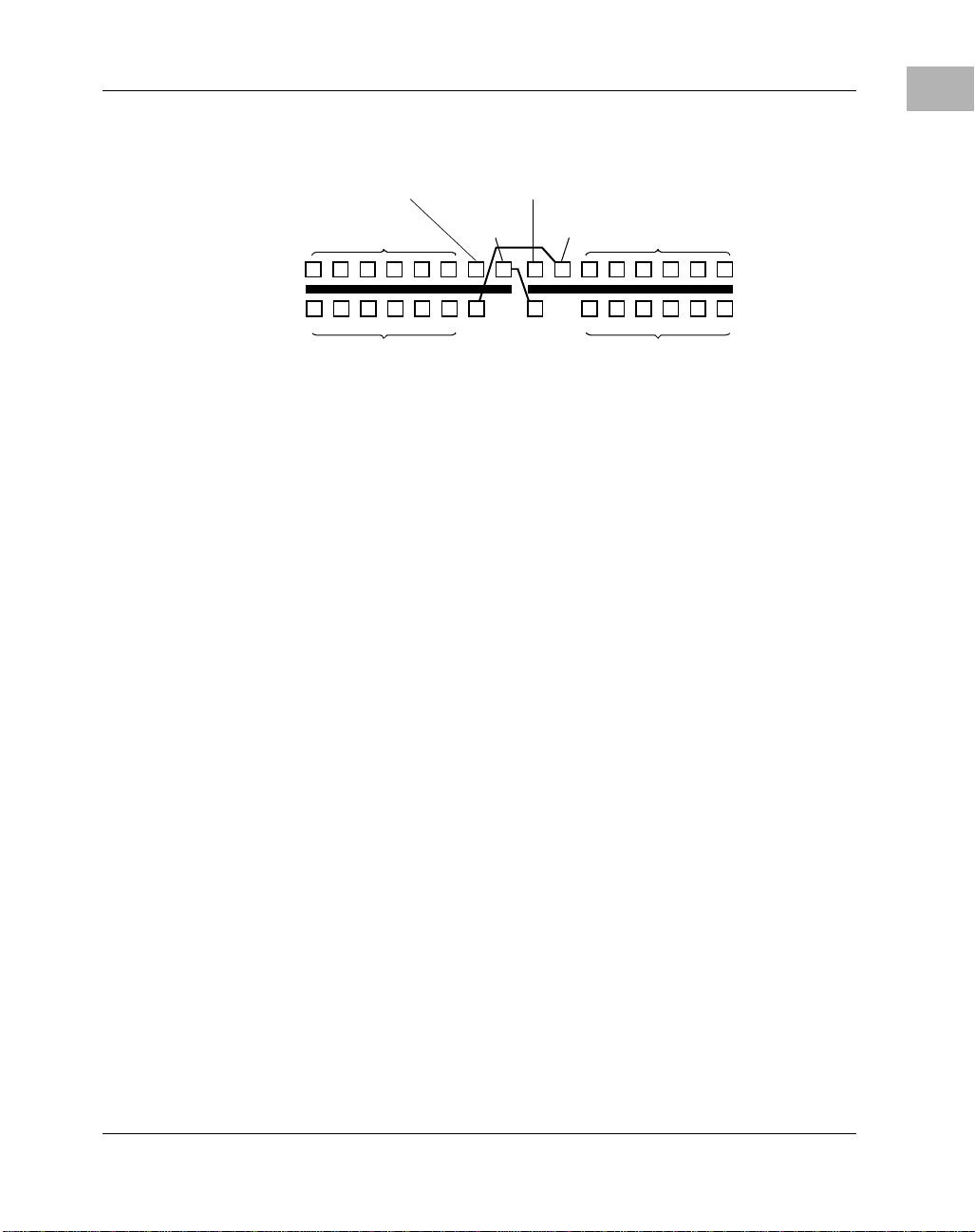
Staged Pin s .. ......... ................. .......... .......... .......... ................. ......... .......... ........ 1 -15
BD_SEL# ............. ...................... ...................... ............... ...................... .......... 1-15
ENUM# ......... .......... .......... ......... ........ ......... .......... .......... ......... ........ ......... ...... 1-15
Contents
vii
Page 8

Hot Swap Control Status Register (CSR) ........................................................ 1-16
The Hot Swap Process ............................................................................................1-16
Physical Connection Process ........................................................................... 1-17
Hardware Connection Process ......................................................................... 1-17
Software Connection Process ..........................................................................1-18
Software Disconnect ion P rocess .................... .. ............ ........................ ...........1-18
Typical Insertion and Extraction Processes ..................................................... 1-19
Devic e D r iv er s ............ .......... ......... ................. .......... .......... ......... .......... ................. 1- 1 9
CHAPTER 2 CPU Modules
Overview .................................................................................................................. 2-1
CPX75 0 H A .......... ......... .......... .......... ................. ......... .......... .......... ................. ......... 2- 1
Connectors and Jumper Settings ....................................................................... 2-4
Backplane Connectors (P5, P4, P3, P2, P1) ................... .......... ..................2-4
Front USB Connectors (J1 7 and J 18) .................... .................... .................2-4
10BaseT/100BaseTx Connector (J8) .........................................................2-4
COM1 Connector (J15) ................ ..............................................................2-5
Debug Connector (J 19) ..............................................................................2-6
DRAM M ez zanine C onn ector (J1 0) .......... .......... ......... .......... ................. 2- 1 0
EIDE Compact FLASH Connector (J9) ...................................................2-14
Flash Bank Selection (J6) ......................................................................... 2-15
CPV5350 ................................................................................................................2-16
Conn ectors ...... ....... ........ ....... ..... ....... ....... ........ ....... ..... ....... ....... ........ ....... ..... ..2-18
Transition Module ......................... ............................... .................... ...............2-19
DRAM Memory Configuration ....................................................................... 2-20
Keyboard/Mouse PS2 Connector ....................................................................2-20
Ethe rne t C on n e ctors ...... ................. ......... .......... .......... ......... ................. .......... 2-2 1
Universal Serial Bus (US B) Conne ctor .......... ............ ........................ ............ .2-21
Serial Port Connectors .....................................................................................2-22
Video Connector .............................................................................................. 2-22
CHAPTER 3 CPX8540 Carrier Card
Overview .................................................................................................................. 3-1
CPX8540 Carrier Car d .............. ........ ................... ........ ................... .........................3-1
Connector Pinouts ..................................................................................................... 3-4
viii
Page 9

CHAPTER 4 PMC Modules
Overvie w ............ .............. ............... ...................... ...................... ..................... ........ 4-1
SCSI-2 Controller PMC ........................................................................................... 4-1
Switc h Se tt in g s ........ .......... ......... .......... ................. .......... ......... .......... .......... ..... 4-3
Conne ct or Pin A ss i g nm en ts ............ .......... .......... ......... ................. .......... .......... 4-4
CHAPTER 5 Transition/Bridge Modules
Overvie w ............ .............. ............... ...................... ...................... ..................... ........ 5-1
CPX750 H ATM Transitio n M o dule . .. ................. .......... .......... ......... ................. ........ 5-1
Serial Ports 3 and 4 Default Configuration ....................................................... 5-2
Serial Port Interface Jumper (J8 and J9) ........................................................... 5-4
Connectors ........................................................................................................ 5-4
Backplane Connectors (J3/J4/J5) ............................................................... 5-4
Asynchronous Serial Port Connectors (J10 and J11) ................................. 5-6
Asynchronous/S ynchronous Serial Port Connectors (J6 and J24) ............. 5-7
Parallel I/O Port Connector (J7) ................................................................ 5-9
Keyboard/Mouse Conne ctor (J16) .................. ............ ............ ................. 5-10
USB Connectors (J19 and J18) ................................................................ 5-10
EIDE Connector (J15) ............................................................................. 5-11
Floppy Port Connector (J 17) .............................................. ........... ........... 5-12
+5Vdc Power Connector (J14) ................................................................ 5-12
Speaker Output Connector (J13) ........................ ........................ ............ ..5-13
PMC I/O Connectors ............................................................................... 5-14
Installing the Serial Interface Modules ........................................................... 5-16
Port Con f ig u ration Dia g r am s .......... ... ......... .......... .......... ......... ................. ...... 5-18
COM1 and COM2 Asynchronous Serial Ports ........................................ 5-18
Asynchronous/Synchronous Serial Ports ................................................. 5-20
CPV535 0 TM80 Transi tion Modu l e ....... ... .. .......... ......... ................. .......... .......... ... 5-29
Connectors ...................................................................................................... 5-31
Keyboard/Mouse PS2 Connector ............................................................. 5-32
Ethernet Connectors ...................................... ............ ........................ ....... 5-33
Serial Port Connectors ............................................................................. 5-33
Video Connector ...................................................................................... 5-34
Parallel Port Connector (J20) ................................................................... 5-35
EIDE Headers (J5) ................................................................................... 5-36
Floppy Header (J9) .............. ........................... .........................................5-38
Keyboard/Mouse/ Power LED Header (J6) ................. ............. ................5-40
USB Headers (J12 and J19) ..................................................................... 5-41
SM Bus and LM78 Header (J1) ............................................................... 5-42
Fan Tachometer Headers (J3 and J4) ....................................................... 5-43
ix
Page 10

Indicator LED/Miscellaneous Header (J2) ............................................... 5-43
CHAPTER 6 Subassembly Reference
Chapt er Over vie w .. ..... ..... ..... .... ... ..... ..... .... ..... ... ..... .... ..... ..... ... .... ..... ..... ..... .. ..... ..... .. 6-1
Parts of the System ................................................................................................... 6-2
CompactPCI Card Cage Reference .......................................................................... 6-4
Backplane Reference ................................................................................................ 6-5
Power Supply Connectors (PS1, PS2, PS3) ......... ............ ........................................6-6
H.110 Power Connector (CPX8216T Only) .............................................................6-7
Alarm Interface Connect or (ALARM) ..... ............ ............ ........................................6-8
Floppy Drive Connectors (FDA, FDB) ....................................................................6-8
IDE Drive Connectors (IDEA and IDEB) ........ ............ ............ .. ............ ..................6-9
Peripheral Power Connectors (PWR1, PWR2, PWR3, PWR4) .............................6-10
Peripheral Signal Connectors (SIG1, S IG2, SIG3, SIG4) ......................................6-11
CompactPCI Connectors (P1, P2, P3, P4, P5)—CPX8216 Sta ndard Backplane ..6-11
Primary (Front) Side I/O Connectors (Slots 1-6 and 11-16) ...........................6-11
Primary (Front) Side CPU Slot Connectors (7 and 9) .....................................6-17
Secondary (Rear) Side I/O Connectors .......... ........................ ............ ............ .6-26
CPU Transition Module Connectors
(Transition Slots 7 and 9) ....................................................................................... 6-27
Hot Swap Controller/Bridge Connectors (Transition Slots 8 and 10) ....................6-29
H.110 Bus Conne ctors—CPX8216T System Only ............................................. ...6-37
Primary (Front) Side I/O Connectors ....................................................................6-38
Primary (Front) Side (Slots 1-6 and 11-16) .................................................... 6-38
Primary (Front) Side CPU Connectors ............................................................ 6-40
Primary (Front) Side HSC Connectors ............................................................ 6-40
Secondary (Rear) Side I/O Connectors ............................. ............ .. ............ .. .........6-50
Secondary (Rear) Side CPU Transition Module Connectors ............... .. ................6-50
Alarm Display Panel ............................................................................................... 6-51
Alarm Display Panel Interface Connector (J 4) ............... .. ............ ..........................6-53
Remote Alarm Connector (J1) ................................................................................6-53
Power Distribution Panel ........................................................................................6-54
AC Power Distribution Panel (CPX8216) ....................................................... 6-54
Dual Input DC Power Distribution Panel (CPX8216) ........ .. ..........................6-55
Dual Breaker DC Power Distribution Panel (CPX8216) ................................6-55
H.110 DC Power Distribution Panel (CPX8216T) ......................................... 6-56
Power Supplies ............... .. ............ .. ............ ............................................................6-58
x
Page 11

APPENDIX A Specifications
Environ m e n tal Characterist i cs ........ .......... ......... ................. .......... .......... ......... ........A -1
Power Supply Electrical Specifications ...................................................................A-2
APPENDIX B Related Documentation
Motorola Comput er Group Documents ....................................... ............................B-1
Related Specifications ..............................................................................................B-2
URLs ........................................................................................................................B-4
xi
Page 12

List of Figures
Figure 1-1. CPX8216 Domains ............................................................................... 1-2
Figure 1-2. CPX8216 Standard System Layout ...................................................... 1-3
Figure 1-3. CPX8216T H.110 System Layout ........................................................ 1-4
Figure 1-4. CPX8216 I/O Bus Connectivi ty ....... ..................... .................... ........... 1-5
Figure 1-5. The CPX8216T H.110 Bus ................................................................. 1-14
Figure 2-1. CPV5350 Component Side View ......... ............ ..................................2-19
Figure 2-2. Keyboard/Mouse Connector Diagram ............................. ................... 2-20
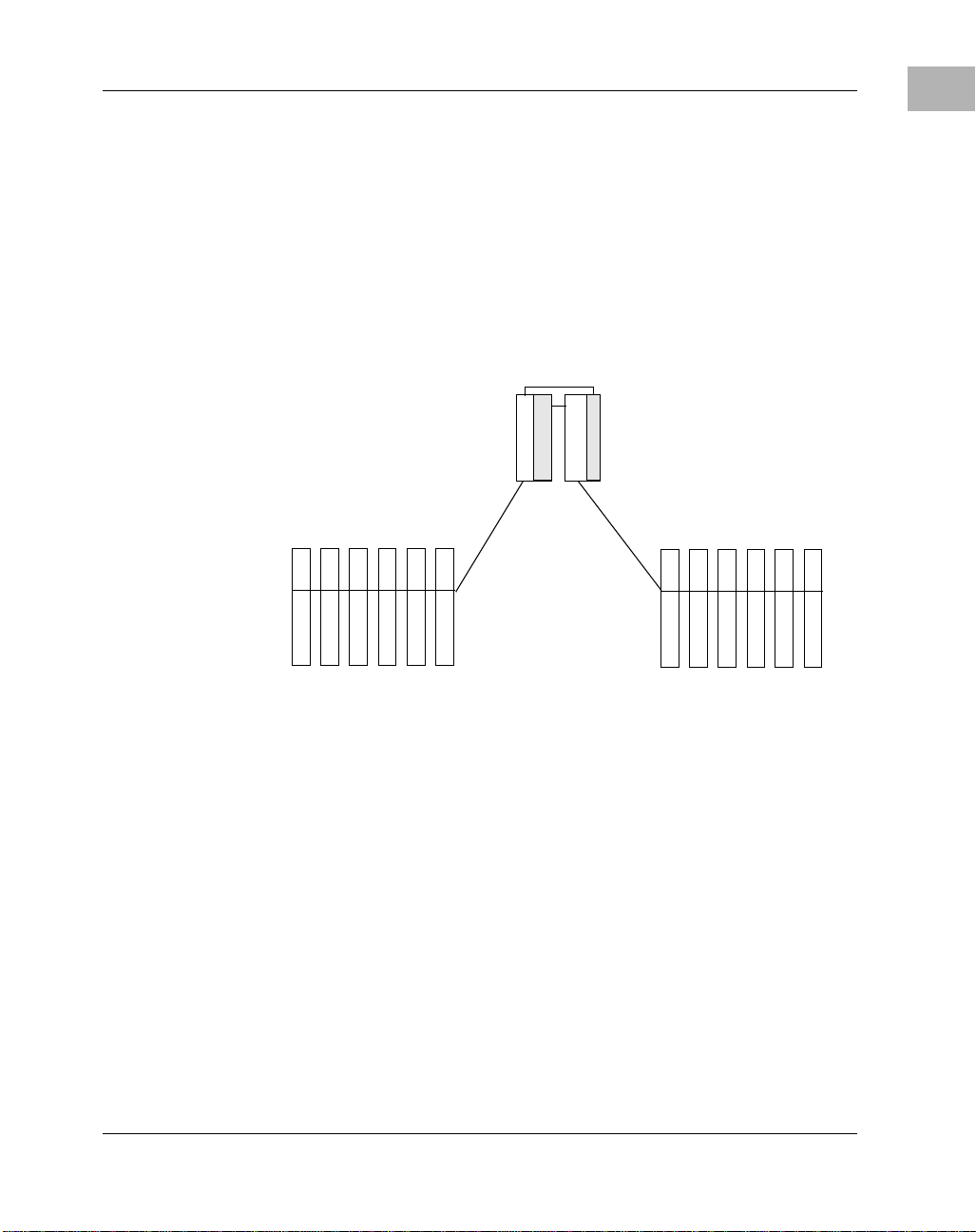
Figure 3-1. PMC Modules to CPX8540 Carrier Ca rd ...... .......... .. .......... ................ 3-2
Figure 3-2. Installing a PMC Module ..................................................................... 3-3
Figure 5 - 1. CPX75 0 H ATM Transition M o du l e ... .. .......... .......... ......... ................. ... 5-3
Figure 5-2. Serial Port Interface Jumper (J9) Settings ............................................ 5-4
Figure 5-3. DTE Port Configuration (COM1 and COM2) ................................... 5-19
Figure 5-4. EIA-232-D DCE Port Configuration (Ports 3 and 4) .... ..................... 5-21
Figure 5-5. EIA-232-D DTE Port Configuration (Ports 3 and 4) ......................... 5-22
Figure 5-6. EIA-530 DCE Port Configuration (Ports 3 and 4) ............................. 5-23
Figure 5-7. EIA-530 DTE Port Configuration (Ports 3 and 4) ............................. 5-24
Figure 5-8. V.35-DCE Port Configuration (Ports 3 and 4) .................................... 5-25
Figure 5-9. V.35-DTE Port Configuration (Ports 3 and 4) .................................... 5-26
Figure 5-10. X.21-DCE Port Configuration (Ports 3 and 4) ................................. 5-27
Figure 5-11. X.21-DTE Port Configuration (Ports 3 and 4) ................................. 5-28
Figure 5-12. Keyboard/Mouse Connector Diagram ....... ....................................... 5-32
Figure 6-1. CPX8216 Front View ........ .. ............ ............ ........... ............ .................. 6-2
Figure 6-2. CPX8216 Rear V iew ........... .................... .. .......... .. ............................... 6-3
Figure 6-3. Card Cage Rail Color Sche m e—C PX8 216 S tandard System .............. 6-4
Figure 6-4. Card Cage Rail Color Scheme—CPX8216T H.110 System ................6-4
Figure 6-5. CPX8216 and CPX8216T Backplan e— Pri mary Side ............ ............. 6-5
Figure 6-6. The CPX8216T H.110 Bus ................................................................. 6-37
Figure 6-7. Alarm Display Panel Block Diagram ................................................. 6-51
Figure 6-8. Alarm Display Panel—Front View .................................................... 6-52
Figure 6-9. AC Power Distribution Panel—Front View ....................................... 6-54
Figure 6-10. Dual Input DC Power Distribution Panel—Front View ................... 6-55
Figure 6-11. Dual Breaker DC Power Distribution Panel—Front View ............... 6-56
Figure 6-12. H.110 DC Power Distribution Panel ................................................ 6-57
xiii
Page 13

List of Tables
T able 2-1. CompactPCI Boards ............................................................................... 2-1
Table 2-2. USB 0 Connector J18 .................................. .................... ....................... 2-4
Table 2-3. USB 1 Connector J17 .................................. .................... ....................... 2-4
Table 2-4. 10BaseT/100BaseTx Connector J8 ......... ............................... ................ 2-5
T able 2-5. COM1 Connector J15 ............................................................................ 2-5
Table 2-6. Debug Connector (J19) ........................... ............ ........................ ...........2-6
Table 2-7. DRAM Mezzanine Connector (J10) .... ............ ............ .. ......................2-10
T able 2-8. EIDE Compact FLASH Connector J9 ................................................. 2-14
Ta ble 2-9. CPV5350 Front Panel Connectors, Board Headers and Components . 2-18
Table 2-10. Keyboard/Mouse P/S2 Connector Pin Assignments (J50) ................2-20
Table 2-11. Ethernet Connector Pin Assignments (J13 and J6) ................ ............2-21
T able 2-12. USB Connector Pin Assignments (J14) ............................................. 2-21
T able 2-13. Serial Port Connector Pin Assignments (J24 and J25) ...................... 2-22
Table 2-14. Video Connector Pin Assignments (J23) ................. .. ............ ............2-22
T able 3-1. CPCI J3 I/O Connector Pinout ............................................................... 3-4
T able 3-2. CPCI J5 I/O Connector Pinout ............................................................... 3-4
Table 3-3. PCI 32-bit Interface Connector P 11/J11, P21/J21 .................... .............3-5
Table 3-4. PCI 32-bit Interface Connector P12/J12, P22/J22 ....... .. .......... .............. 3-7
Table 3-5. PCI 64 bit PCI extension on PMC Connector J13, J23 .............. .......... . 3-8
Table 3-6. User-Defined I/O PCI Interface Connector P14/J14, P24/J24 ........... .... 3-9
T able 4-1. PMC Switch Settings ............................................................................. 4-3
T able 4-2. PMC Pin Assignments ........................................................................... 4-4
T able 5-1. System Components ............................................................................... 5-1
T able 5-2. J3 User I/O Connector ............................................................................ 5-5
T able 5-3. J5 User I/O Connector ............................................................................ 5-6
T able 5-4. COM1 (J11) and COM2 (J10) ............................................................... 5-7
T able 5-5. Serial Port 3 (J6) .................................................................................... 5-7
T able 5-6. Serial Port 4 (J24) .................................................................................. 5-8
Table 5-7. Parallel I/O Connector (J7) ........................................ ............ .. ............ .. 5-9
Table 5-8. Keyboard/Mouse Connector (J16) .......... ............ .. ............ ............ .. ..... 5-10
T able 5-9. EIDE Connector (J15) ...........................................................................5-11
Table 5-10. Floppy Connector (J17) ........... .. .................................. ........... ........... 5-12
T able 5-11. +5Vdc Power Connector (J14) ........................................................... 5-13
Table 5-12. Speaker Output Connector (J13) ...................... ..................................5-13
xv
Page 14

Table 5-13. PMC I/O Connector (J2) ....................................................................5-14
Table 5-14. PMC I/O Connector (J21) ..................................................................5-15
Table 5-15. Keyboard/Mouse P/S2 Connector Pin Assignments (J14) ......... ........5-32
Table 5-16. Ethernet Connector Pin Assignments (J13 and J18) ..........................5-33
Table 5-17. Serial Port Connector Pin Assignments
(J21 and J10) ...........................................................................................................5-33
Table 5-18. Video Connector Pin Assignments (J16) ............................................5-34
Table 5-19. Parallel Connector Pin Assignments (J20) ......................................... 5-35
Table 5-20. EIDE Header (J5) Pin Assignments ................................................... 5-36
Table 5-21. Floppy Header (J9) Pin Assignments .................................................5-38
Table 5-22. Keyboard/Mouse/Power LED Header (J6) Pin Assignments ............5-40
Table 5-23. USB Headers (J12 and J19) Pin Assignments .................................... 5-41
Table 5-24. SM Bus and LM78 Header (J1)Pin Assignments ..............................5-42
Table 5-25. Fan Tachometer Header (J3 and J4) Pin Assignments ....................... 5-43
Table 5-26. Indicator LED/Miscellane ous Header (J2) Pin Assignments .............5-43
Table 6-1. System Components ...............................................................................6-1
Table 6-2. PS1, PS2, and PS3 Pin Assignments ......................................................6-6
Table 6-3. Fan Module P in As si gn ments ......... ......... .......... .......... ................. ......... 6-7
Table 6-4. H.110 Power Connector .........................................................................6-7
Table 6-5. ALARM Connector Pin Assignments ....................................................6-8
Table 6-6. FDA and FDB Pin Assignments ............................................................6-8
Table 6-7. IDEA and IDEB Pin Assignments ......................................................... 6-9
Table 6-8. PWR1, PWR2, PWR3, PWR4 Pin Assignments ................................. 6-10
Table 6-9. SIG1, SIG2, SIG3, SIG4 Pin Assignments .......................................... 6-11
Table 6-10. P5 Connector, I/O Slots 1-6 and 11-16
(User I/O) ................................................................................................................ 6-12
Table 6-11. P4 Connector, I/O Slots 1-6 and 11-16 (User I/O) ............................. 6-12
Table 6-12. P3 Connector, I/O Slot s 1-6 and 11-16 (User I/O) .............................6-12
Table 6-13. P2 Connector, I/O Slots 1-6 and 11-16 (CP CI Bus ) ...........................6-13
Table 6-14. P1 Connector, I/O Slots 1-6 and 11-16 (CP CI Bus ) ...........................6-14
Table 6-15. P5 Connector, CPU Slots 7 and 9 .......................................................6-17
Table 6-16. P4 Connector, CPU Slots 7 and 9 .......................................................6-18
Table 6-17. P3 Connector, CPU Slots 7 and 9 .......................................................6-20
Table 6-18. P2 Connector, CPU Slot 7 (Domain A) ..............................................6-20
Table 6-19. P2 Connector, CPU Slot 9 (Domain B) ..............................................6-22
Table 6-20. P1 Connector, CPU Slots 7 and 9 .......................................................6-23
Table 6-21. P5 Connector, I/O Slot s 1-6 and 11-16 (User I/O) .............................6-26
Table 6-22. P4 Connector, I/O Slot s 1-6 and 11-16 (User I/O) .............................6-26
Table 6-23. P3 Connector, I/O Slot s 1-6 and 11-16 (User I/O) .............................6-26
xvi
Page 15

Table 6-24. P5 Connector , CPU Transiti on Module Slots ........................ ............6-27
T able 6-25. P3 Connector, CPU Transition Slots 7 and 9 ..................................... 6-28
T able 6-26. P5 Connector, HSC/Bridge (Slots 8 and 10) ...................................... 6-29
T able 6-27. P4 Connector, HSC/Bridge (Slots 8 and 10) ...................................... 6-29
T able 6-28. P3 Connector, HSC Slots 8 and 10 .................................................... 6-31
T able 6-29. P2 Connector, HSC Slot 10 ................................................................ 6-32
T able 6-30. P2 Connector, HSC Slot 8 .................................................................. 6-34
T able 6-31. P1 Connector, HSC Slots 8 and 10 .................................................... 6-35
T able 6-32. P4 Connector, I/O Slots 1-6, 11-16 .................................................... 6-38
T able 6-33. P5 Connector, HSC/Bridge (Slots 8 and 10) ...................................... 6-40
T able 6-34. P4 Connector, HSC Slots 8 and 10 .................................................... 6-42
T able 6-35. P3 Connector, HSC Slots 8 and 10 .................................................... 6-44
T able 6-36. P2 Connector, HSC Slot 10 ................................................................ 6-45
T able 6-37. P2 Connector, HSC Slot 8 .................................................................. 6-47
T able 6-38. P1 Connector, HSC Slots 8 and 10 .................................................... 6-48
T able 6-39. P5 Connector, I/O Slots 1-6 and 11-16 (User I/O) ............................. 6-50
T able 6-40. P3 Connector, I/O Slots 1-6 and 11-16 (User I/O) ............................. 6-50
T able 6-41. Alarm LED Color and Description .................................................... 6-52
T able 6-42. Alarm Display Panel Interface Connector (J4) .................................. 6-53
Table 6-43. Remote Alarm Connector (J1) .............. ............ .. ............ ................... 6-53
T able 6-44. DC Analog Voltages for H.110 Bus ................................................... 6-57
T able A-1. Total Regulation (per Output) ...............................................................A-3
T able B-1. Related Specifications ...........................................................................B-2
xvii
Page 16
About this Manual
This manual is directed at the per son who needs de tailed configur ation a nd
specification information for CompactPCI modules and system
subassemblies of the CPX8000 series computer system. Included is an
overview of the system archite cture for the CPX8216 and CPX81216T
systems. It also presents the corr ect strapping and pin-out information for
the modules and subassemblie s covered.
This manual does not provide installation, removal, or use procedures.
People requiri ng this type of information should refer to the CompactPCI
CPX8216 and CPX8216T System Installa tion and Use man ual as listed in
Appendix B, Related Documentation.
Summary of Changes
This manual has been revised and replaced any previous editions. Below
is a history of the changes affecting this manual.
Date Change
July 2002 Updated PMC Module chapter, see Chapter 4, PMC
Modules.
Load sharing information a dded, see The Act ive/A ctiv e or
Load-Sharing Configuration on page 1-9
Domain ownership further def ined, see Chapt er 1, System
Architecture
Dual breaker DC power distribution panel information
added (with Smart cabl e), see D u a l Breake r DC Power
Distribution Panel (CPX8216) on page 6-55.
April 2002 Section describing system domains and domai n
ownership information added, see System Domains on
page 1-1.
Section describing hot swap controllers added, see Hot
Swap Controller on page 1-6.
xix
Page 17
Date Change
Power distribution information added, see Power
Distribution Panel on page 6-54.
August 2001 Details about assi gning chassis IDs on the CPX8216T
system added. See Chassis ID for CPX8216T on page
1-13.
Updated model numbers , see Systems Supported in this
section.
April 2001 Added cautions regarding hot swap software and hot
swappable drives.
July 2000 Updated pin assignment table s for connector P2
(HSC and CPU slots.)
March 2000 DC Input vol tage change d to - 36Vdc to -72Vd c. Change d
URLs to reflect new Web sites.
November 1999 Added System Architecture chapter.
Added TNV branch circuit safety standards information.
Added the Index.
August 1999 Added information for the CPV5350 Intel CPU
Added information for the H.110 Backplane and Power
Distribution Pane l for the CPX8216T system
xx
May 1999 Replaced Figure 2-1 with corrected board illustration
January 1999 Original Document
Page 18
Systems Supported
This information in this manual applie s to the modules and subassemblie s
supported by the following systems:
Model N u m b er Descript i o n
CPX8216SK24 CPX8216 Dual SCSI 466 MHz PowerPC Starter Kit,
CPX8216TSK24 CPX8216T Dual EIDE 700 MHz Pent ium Star ter Kit,
CPX8216SK25 CPX8216 Dual EIDE 700 MHz Pentiu m Sta rter Kit,
CPX8216TSK25 CPX8216T Dual EIDE 466 MHz PowerPC Starter
256MB
512MB
512MB
Kit, 256MB
xxi
Page 19

Overview
This manual is divided into the followi ng topic s:
❏ Chapter 1, System Architecture
❏ Chapter 2, CPU Modules
❏ Chapter 3, CPX8540 Carrier Card
❏ Chapter 4, PMC Modules
❏ Chapter 5, Tr ansition/Bridge Modules
❏ Chapter 6, Subassembly Reference
❏ Appendix A, Specifications
❏ Appendix B, Related Documentation
Comments and Suggestions
Motorola welcomes and appreciates your comments on its documentati on.
W e want to know what yo u think about our manuals and how we can make
them better. Mail comments to:
Motorola Computer Group
Reader Comments DW164
2900 S. Diablo Way
T empe, Arizona 85282
xxii
You can also submit comments to the following e-mail address:
reader-comments@mcg.mot.com
In all your c orrespondence, please list your name, position, and company .
Be sure to include the title and part number of the manua l and tell how you
used it. Then tell us your feelings about its str engths and weaknesses and
any recommendations for improvements.
Page 20

Conventions Used in This Manual
The following typographi cal c onventions are used in this document:
bold
is used for user input that you typ e ju st as it appe ars; it is als o used for
commands, options and arguments to commands, and names of
programs, directories and files.
italic
is used for names of varia bles to which you assign value s. Italic is also
used for comments in sc ree n displays and examples, and to introduce
new terms.
courier
is used for system output (for example, sc reen displays, reports),
examples, and system prompts.
<Enter>, <Return> or <CR>
represents the carriage return or Enter key.
Ctrl
represents the Contr ol key. Execute control characters by pr essing the
Ctrl key and the letter simultaneously, for example, Ctrl-d.
xxiii
Page 21

1System Architecture
PICMG Compliance
The CPX8216 system is designed to be fully complia nt with the
CompactPCI Hot Swap Specification developed by the PCI Industrial
Computers Manufacturi ng Group (PICMG). With the proper software
support and testing, it should be possible to integrate all propri etary and
third-party I/O modul es which are compatible with this specificat ion.
Further , the system allows the use of I/O modules which are not hot
swappable, but the system must be powered off when such modules are
inserted and extract ed .
The CPX8216 also fe atures the ability to hot swap system and nonsystem
processor boards, a feature which is beyond the scope of the PICMG
specification. As part of its c ommitment to open standards, Motorola will
propose that th e proce ssor ho t swap c apabilit ie s of th e CPX8216 be added
to the Hot Swap Specification. At this point, however, there are no thirdparty CPU modules which are compatible with the CPX8216 syst em.
1
System Domains
The high availa bility a nd high slot coun t of th e CPX8216 sys tems i s made
possible by implementing two host CPU slots a nd multi ple CompactPCI
bus segments in a single chassis. These bus segments, along with other
system resources are grouped into two logical domains, A and B, which
can be controlle d by either host-HSC pair r egardless of the bus se gment the
host sits on. Domain A includes C ompactPCI bus segment A (sl ots 1 to 8),
the power supply/fan tray modul es and alarm controls. In the CPX8216,
domain B consists of the CompactPCI bus segment B (slots 9 to 16). For
further information on domain c ontrol or ownership, see the section, Hot
Swap Contr oller on page 1-6.
1-1
Page 22
1
System A rchitecture
Al arm Controls
Domai n A Domain B D om a in A/B
Figure 1-1. CPX8216 Domains
System Layout
The CPX8216 is a 16-slot, high-avail abilit y CompactPCI system with two
separate 6-slot CompactPCI I/ O domains and the capa bility to contain
redundant CPU modules and redundant Hot-Swap Controller (HSC)
modules. It is also possible to configure the sy stem as a simplex, h igh I/O
system containing a single CPU-HSC pair. Eve n as a simplex system, the
CPX8216 still provides improved availability through redundant powe r
supplies and the control/moni toring capabilities of the HSC, as described
in The Hot Swap Controll er/Bridge (HSC) Module on page 1-5.
Bus A Bus B
Power Supply/Fan Trays
Drive
Bays
CPX8216
The CPX8216 standard system consists of two 8-slot subsystems, or
domains, each with two slots for the host proces sor and six slots for
nonhost CompactPCI boards. The HSC board mounts in the rear of the
chassis, behind the s econdar y CPU slot. Figur e 1-2 on pa ge 1-3 pr ovides a
diagram of this configuration.
1-2 Computer Group Literature Center Web Site
Page 23
CPX8216
Rear Card Locations
Segment A
CPU Transition Module
Segment B
Transition Slots
1234567 9 111213141516
Segment A
I/O Slots
Compact PCI
Segment A
Segment B
CPU Transition Module
Segment B
Front Card Locations
HSC
Segment A
HSC
Segment B
Transition Slots
Segment B
I/O Slots
Compact PCI Bus
Segment B
2450 9812
Figure 1-2. CPX8216 Standard System Layout
Each of the two independent I/O domains has its own system processor
slot. Each system processor has direct access to its local bus through an
onboard PCI-to-PCI (P2P) bridge. Each domain is also capable of
supporting a Hot Swap Con troller ( HSC) module that cont ains its own P2P
bridge. Thus, in a f ul ly redunda nt configurati on, there are two bridge s tha t
have access to ea ch of the I/O buses—one assoc iated with the CPU and one
with the HSC. Only one of the bridges may be active at a time, however.
1
http://www.motorola.com/computer/literature 1-3
Page 24
1
System A rchitecture
CPX8216T (H.110)
The CPX8216T H.110 system consists of two 8- slot subsystems, or
domains, each with one slot for the host processor, one slot for the frontloaded HSC, and six slots for nonhost CompactPCI boards. F igure 1-3 on
page 1-4 provides a diagram of this configuration.
Rear Card Locations
Segment A
CPU Transition Module
Segment B
CPU Transition Module
Segment B
Transition Slots
1234567 9 111213141516
Segment A
I/O Slots
Compact PCI
Segment A
CPU
A
Segment B
HSC
Front Card Locations
Figure 1-3. CPX8216T H.110 System Layout
Bus Access and Control
In the fully redundant configur ation, the CPU in the left system slot, CPU
A, is associated with the HSC in t he right HSC slot, HSC A (note th at HSC
A actually sits on the Domain B bus). The re is a l ocal connec tion betwe en
each CPU-HSC pair that allows the CPU in one domain to control the other
domain through its HSC. This architecture is illustrated in the following
figure.
810
CPU
B
Segment A
HSC
Segment B
Transition Slots
Segment B
I/O Slots
Compact PCI Bus
Segment B
1-4 Computer Group Literature Center Web Site
Page 25
The Hot Swap Controller/B ridge (HSC) Module
S p e c ia l B a c k p la n e
P C I Inte r co n n e c ts
C
H
H
C
P
U
A
S
P
S
C
U
C
A
B
B
1
I/O D o main A
I/O
I/O
S
S
L
L
O
O
T
T
I/O
I/O
I/O
I/O
S
S
S
L
L
O
O
T
T
S
L
L
O
O
T
Primary CompactPCI
T
Buses
I/O D o m a in B
I/O
I/O
S
S
L
L
O
O
T
T
I/O
I/O
I/O
I/O
S
S
S
L
L
O
O
T
T
S
L
L
O
O
T
T
Figure 1-4. CPX8216 I/O Bus Connectivity
In addition to provi ding bridges t o the remote I/O bus es, the HSC provides
the services necessar y to hot swap CPU boards and nonhost proces sor
boards and also contro ls the system ala rm panel, fans, and power suppli es.
The Hot Swap Controller/Bridge (HSC) Module
The HSC module connect s to the CPU module through a loc al P CI bus, as
illustrated in Figure 1-2 and Figure 1-3. The HSC module contains a PCI-
to-PCI bridge and also contains a Hot Swap Controller .
The functionalit y provided by the HSC is at the heart of the High
Ava ilability CPX8216 System. Its primary functions include:
❏ Providing a bridge between the two ei ght-slot CompactPCI buses
so that they can be managed by a single CPU module
❏ Maintaining a Control Status Register whi ch contains in formation
on the status of each system module
http://www.motorola.com/computer/literature 1-5
Page 26

1
System A rchitecture
❏ Controlling power and resets to each system module through
radial connections
❏ Monitoring and controlling CPU boards, nonhost boar ds, a nd
peripherals, including power and fan sleds, board and system
LEDs, and alarms
Hot Swap Controller
Each of the nonhost slots in the syste m can be controlled from either HSC.
When an HSC has control over a domain it has control over the nonhost
boards in that domain. Each host processor /br idge pair is controlled as a
single item by the other processor/bridge pair. The bridge and the host
processor are linked together so tha t both must be present for power to be
applied. A host processor cannot be operate d without its HSC.
With the CPX8216 a rchitectur e it is importa nt that the syste m initializes t o
a state that allows the host processor s and HSCs to be in control of the
system. The default conditions are:
❏ System processors an d bridges are powered up (if present)
❏ System processors an d bridges are disconne cted from their busses
❏ HSCs are not in control of either domain
❏ Nonhost boards are powered off
❏ Peripheral bay s are pow e red u p (if pres en t)
❏ Fans and power supplies are powere d on
Note System components such as fans and power supplies may be
controlled by e ither HSC but not both. Def ault cont rol belongs to
Domain A and whichever HSC has control of Domain A has
control of the system functions .
If Domain A is not controlled, nonhost boards are powere d- off
and all LED updates to the display panel and power supplies are
suspended. Also, monitoring of alarm inputs from the display
panel and power supplies are inhibited.
1-6 Computer Group Literature Center Web Site
Page 27

System Process o r Config urati o n s
Subsequent to the default, the system software must determine the
configuration of the system and then proceed to change it.
System Processor Configurations
The CPX8216 is a flexib le system that allows for multiple configurations
of processor control, I/O redundancy, and peripheral configur ations. The
following sections br iefly touch on possible configurati ons.
As noted above, there are three possible processor/control configurations:
❏ A simplex system conta ining a single CPU-HSC pair controlling
both I/O domains
❏ An active/pa ssive configuration simila r to the simpl ex
configuration , but providing a warm backup for bot h the CPU and
the HSC
❏ An active/active or load-sharing configuration in which each CPU
runs a single domain while also serving a s a backup to the othe r
CPU.
Note H.110 traffic and HA Linux do not support a load-
sharing configura tion.
1
The following sections give a general de scription of these configurations.
The Simplex Configuration
Because of the flexible nature of the CPX8216, it is possible to configure
it with different lev el s of redundancy and availability. For applications
which do not require the benefits of full high availability, it is possible to
configure the CPX8216 as a simplex, 16-slot system. This configuration
provides the benefits of redundant power supplies and the system
monitoring capabilities of the fully redundant configuration.
http://www.motorola.com/computer/literature 1-7
Page 28
1
System A rchitecture
The simplex configuration is illustrated in the following figure.
I/O D o main A
I/O
I/O
I/O
I/O
I/O
I/O
S
S
S
S
S
L
L
L
O
T
L
O
O
O
T
T
T
S
L
L
O
O
T
T
The Activ e/Pa ssive Configu r ati on
In the active/passi ve configuration , one CPU manages all twelve I/ O slots,
much like in the simplex confi guration. In addition, th e second CPU serves
as a warm standby, ready to run the system in the event of a failure on the
active system.
The active/passive confi gur ation is illustrated in the following figure.
Active CPU
C
P
U
A
H
S
C
A
I/O D o main B
I/O
I/O
I/O
I/O
I/O
I/O
S
S
S
S
S
L
L
L
O
O
T
T
C
H
H
C
P
U
A
S
P
S
C
U
C
A
B
B
Activ e HS C
L
O
O
T
T
S
L
L
O
O
T
T
I/O Domain A
Passive
I/O Domain B
CPU/HS C
I/O
I/O
I/O
I/O
I/O
I/O
S
S
S
S
S
L
L
O
T
L
O
O
O
T
T
S
L
L
L
O
O
T
T
T
I/O
I/O
I/O
I/O
I/O
I/O
S
S
S
S
S
L
L
L
O
O
T
T
L
O
O
T
T
S
L
L
O
O
T
T
1-8 Computer Group Literature Center Web Site
Page 29
The Active/Active or Load-Sharing Configuration
The Active/Ac tive or Load-Sharing Confi guration
In the load sharing configu ration, each CPU manages si x of the twelve I/O
slots, much like a dual 8-slot system with the added benefit of one CPU
being able to control all twelve I/O slots if the other CPU fails. It is
important in a load-shar ing configuration to note that the total cri tical
activity does not exceed the capabilities of a single CPU, because either
one of the C PUs must be ready to take over the loa d carried by the other.
The active/activ e confi guration is illustrated in the following figure.
H
C
H
C
P
S
S
P
U
A
C
U
C
AB
B
1
I/O D o main A
I/O
I/O
S
S
L
L
O
O
T
T
I/O
I/O
I/O
I/O
S
S
S
L
L
O
O
T
T
S
L
L
O
O
T
T
I/O D o m a in B
I/O
I/O
S
S
L
L
O
O
T
T
I/O
I/O
I/O
S
S
L
O
T
S
L
L
O
O
T
T
Note H.110 traffic and HA Linux do not support a load-sharing
configuration .
I/O
S
L
O
T
http://www.motorola.com/computer/literature 1-9
Page 30

1
System A rchitecture
I/O Configurations
The CPX8216 contains two independent 8-slot Co mpactPCI buses. One
slot in each bus is dedicated to a system processor, and another is needed
for the HSC. This leaves six slots on each bus to support I/O devic es or
nonsystem processors.
One possible configuration is to use the CPX8216 as a high I/O
CompactPCI system with redundant CPUs. With this configuration, it is
possible to run twelve independent I /O modul es within a CPX8216
system. Applications requiring dense processing power could use all
twelve I/O slots to support nonsystem processors.
Such a system would be protecte d against a CPU or HSC fault, but it would
be vulnerable to data losses if any of the I/O modules or nonsystem
processor modules were to fail. In syste ms handling critical data, it is
possible to implement a 2N or an N+1 I/O redundancy str ategy that allows
the level of service to be continued in the event that a module fails.
In the case of a 2N-redundant system, each I/O module or nonsystem
processor module is matched with an identical module on the other bus.
The paired modules can be configur ed in an active/passi ve arrangement or
a load-sharing arrangement in wh ic h each carri es h al f of the load of a
single module. In an N+1 ar rangement, multi ple modules a re backed up by
a single spare. For example, a single passive nonsystem processor module
can be used to back up five others.
Peripherals
Power/Fan Modules
The CPX8216 system requires a minimum of two power/fan sled modules
and a fan-only sled module to provide adequate power and cooling for a
fully loaded, nonredundant system. The system can c onta in a third power
supply/fan sled a s part of an N+1 strategy, meaning that the system can
continue providing se rvice if one of the mod ules fails. These modules are
hot swappable and available for DC and AC environments.
1-10 Computer Group Liter ature Center Web Site
Page 31

The fans run at e ither high speed (def ault) or temperatu re controlled, which
!
Caution
can be changed using the operatin g syste m software via the API.
Drive Modules
The CPX8216 contains four hot-swappa ble peripheral bays, all of which
support both S CSI and EIDE protocols.
Drive Modules
1
Caution
The hot swapping of hard drive s is supported when your system is
configured with the appropriate software support for hot swap and when
the drives a re in a hot-swap drive carrier.
SCSI devices can be conf igured to be fully hot -swappable, and data can be
hot switched between two inde pendent SCSI controllers. EIDE devices are
assigned to a single EI DE contr oller . They can be wa rm swapped, m eaning
that a failed device can be replaced once the controller has been powered
off.
The rear of the CPX8216 chassis may be configured with either single or
double, fixed, floppy dr ives. Floppy drives are not hot-swappable.
For more information on instal ling both hot-swappable and non-hotswappable drives, refer to the Drive Removal and Installation chapter of
the CPX8216 and CPX8216T CompactPCI System Installation and Use
manual.
http://www.motorola.com/computer/literature 1-11
Page 32

1
System A rchitecture
CPU Complex Architecture
The CPU complex in the CPX8216 contains two CPU modules and their
corresponding Hot Swap Controller (HSC) modules. The figure below
illustrates the architecture, including elements on the boards as well as
local connections between the CPU modules and the PCI-to-PCI (P2P)
connections to the local CompactPCI buses.
Local Conne ct i ons between CPU Modules
Enet
Serial
Link
ISA
IDE
The CPU Module
In addition to the processor, RAM, etc., each CPU module contains one:
❏ Up to two Ethernet controllers
❏ Up to two serial communications links
❏ P2P bridge to the local CompactPCI bus
❏ Local PCI Bus connection to the HSC
Proc
P2P
RAM
HSC
P2P
HSC
P2P
RAM
P2P
CompactPCI BusCompactPCI Bus
Proc
Enet
ISA
IDE
Serial
Link
1-12 Computer Group Liter ature Center Web Site
Page 33

Switching Service to the Passive CPU
The switchover from one CPU to another is initia te d by the passive CPU
when there is an indication tha t there is something wrong with the active
CPU--such as a failed heartbe at protocol. The passive side notifies the
active side t hat it is about to begin a switchover process. I f the active side
agrees to the switc hover, then the two si des coordinat e the hand-of f and no
bus signals, clocks, or devices should be corrupted. If the active system
fails to cooperate with the takeover atte mpt, the n we mus t assume that b us
signals, clocks, and devices attached to the bus may be corrupted.
In a more e xtreme ta keove r , i t i s pos sibl e for the passi ve CPU to powe r -on
reset the active CPU and to take control that way.
Chassis ID for CPX8216T
A unique 5-bit chassis ID can be assigned for each CPX8216T system.
Hex values are on the r otary switches locate d on the HSC boards. A jumper
can be added to J14 to double the number of unique identifiers. This
feature should be used if more than 15 chassis a re deployed in one locatio n.
The HSC boards are shipped wi th no j umper as the def ault. For gui de lines
on setting the chassis ID on yo ur CPX8216T system, refer to the CPX8000
Series CPX8216 and C PX8216T CompactPCI System Install ation and Use
manual.
Switching Service to the Pa ssive CPU
1
Alarms and LEDs
In order to provide a uniform appear ance, without depending on individual
board manufa ct u rers, the CPX8216 con tai ns a se parat e al arm display
panel, which runs across the top of the chassis. In addition to In
Service/Out of Service LED indicators for all sixteen slots, the alarm
display panel contains LEDs for system status (System in
Service/Component out of Service/System out of S ervice) and for the thre e
standard Telco levels (Critical/Major/Minor ). The three Telco alarms are
also signalled through a dry contact relay.
http://www.motorola.com/computer/literature 1-13
Page 34

1
System A rchitecture
H.110 Telephony Bus
The CPX8216T supports an H.110 Computer Telephony Bus. The H.110
bus uses P4/J4 as defined in the PICMG specification for CompactPCI.
P5
P4
P3
P2
P1
H. 110 Bus
CompactPCI Bus
System Slot
HSC Slot
2557 9906
Figure 1-5. The CPX8216T H.110 Bus
Board Insertion and Extraction Features
The PICMG specificat ion detail s sof tware and hardwar e fea tures, i n orde r
to support hot swapping of I/O boards. Hardware features include:
❏ Staged pins that contr ol voltages when inserting or extracting
boards
❏ BD_SEL#, HEALTHY#, and ENUM# signals
❏ Hot swap control status register
1-14 Computer Group Liter ature Center Web Site
Page 35

Staged Pins
Staged P i n s
1
The PICMG CompactPCI hot swap specification provides for three
separate pin lengths in order to control the insertion and extraction
voltages and to notify the syste m when boards are inserted or extracted.
The longest pins, which include VCC pins and GND pins, are the first to
mate during the insertion pr ocess a nd the last to break contact during
extraction. These pins are used to supply power to pre-charge the PCI
interface signals to a neutral state before they contact the bus. This precharging se rves to min imize the c apa citive effects of the board as it makes
or breaks contact with the bus.
The medium-length pins carry PCI and other signal traffic.
The shortest pins are used to asser t signals, including BD_SEL#. During
insertion, the BD_SEL# si gnal ena bles the board to at tach to the local P CI
bus. On extraction, it cause s the board to logically and electricall y
disconnect from the PCI bus before the bus pins physically break contact
with the bus.
BD_SEL#
BD_SEL# is asserted by one of the pins that mate last on insertion and
break first on extr actio n. On inser tion , the signal t ells t he boa rd to conne ct
to the PCI bus. On extraction this pin breaks first, causing the board to
logically and elect ri cally disconnect from the PCI bus before the PCI bus
pins physically break contact with the bus.
ENUM#
An ENUM interrupt is generated when a boar d is ho t inse rt ed into the
CPX8216 chassis, or when an operator trips the board microswitch by
raising its ejector handles. The signal informs the active CPU that the
status of a board ha s changed. The CPU then identifie s the board by polling
the INSert a nd EXTract bits in all of the boards’ Control Status Registers.
http://www.motorola.com/computer/litera ture 1-15
Page 36

1
System A rchitecture
Hot Swap Control Status Register (CSR)
The CPX8216 supports hot swap CompactPCI cards with the standar d
control status regis ter defined by the PICMG Hot Swap Specification . The
register is visibl e in PCI configuration space and pro vides hot swap control
and status bits: INS and EXT. The INS signal is set when ENUM# is
asserted by a board being inserted into the system. The EXT signal is
asserted when ENUM# is asserted by an operator triggering the
microswitch in the board handles. The host also uses these bits to
acknowledge and de-assert ENUM#.
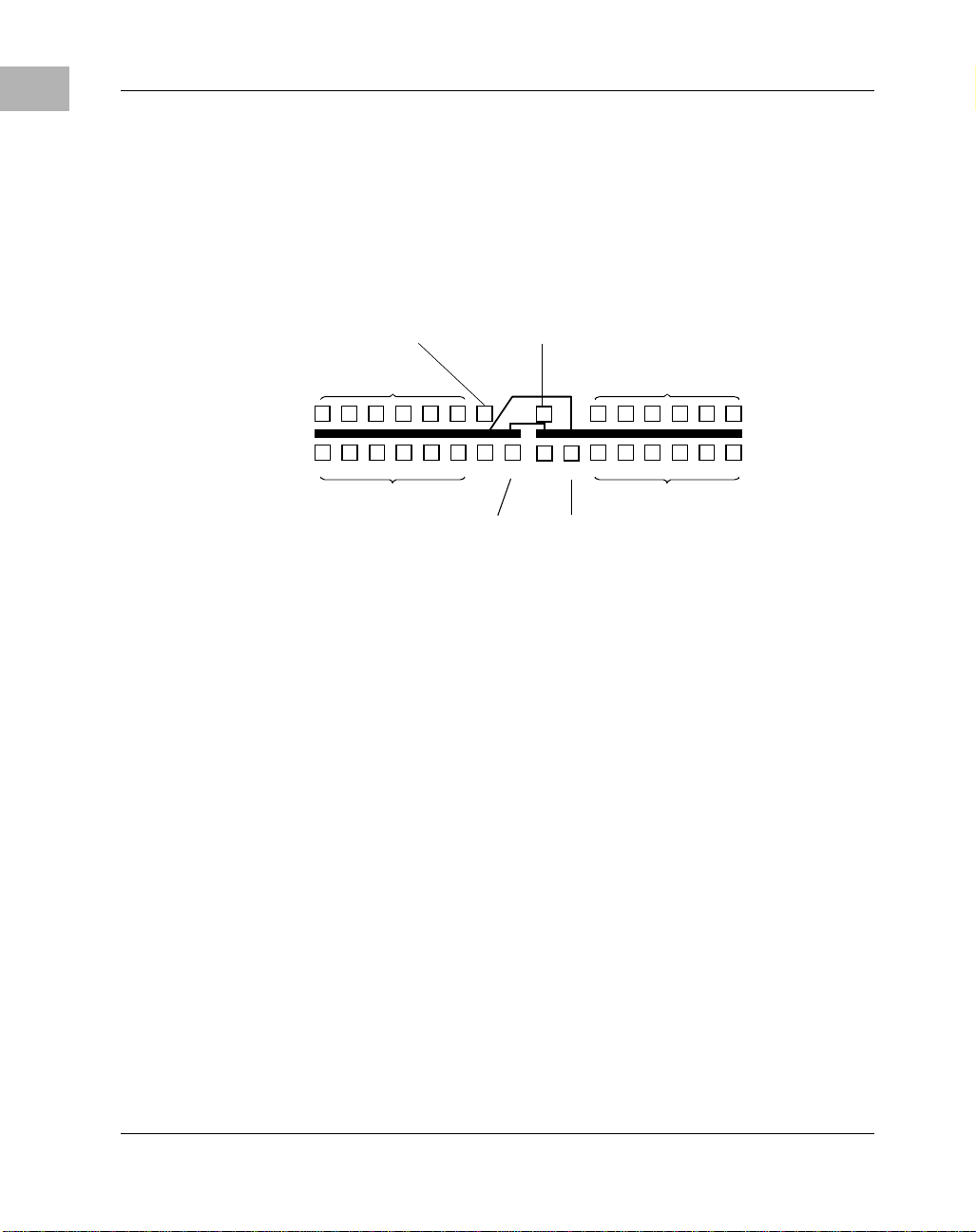
The Hot Swap Process
PICMG divided the complete hot swap process into physical, hardware
and softw are connection processes. These processes are formally brok en
down further int o a group of transit iona l stat es, wh ich are i llust rated in t he
following figure.
PHYSICAL
CONNECTION
STATES
P0 P1
H0 H1
HARDW ARE
CONNECTION STATES
H1F
SOFTW ARE
CONNECTION
STATES
H2
S0 S2 S3
S1
S2Q S3Q
When inserting a board, it goes through all states f rom P0 to S3.
Conversely, a board transitions from S3 to P0 before being extracted.
During normal operation, no states are skipped. Extracting a board in a
software connection st ate other than S0 is l ikely to disrupt software enoug h
to crash the system, b ut the C ompactPCI bus , from a purely ele ctrical poi nt
of view , will not be disrupted enough to cause logic levels to be viol ated.
Certain states are overlapping. For example, when the board is fully seated
(completed P1), but has not yet started the hardware connection process
1-16 Computer Group Liter ature Center Web Site
Page 37

(H0), it said to be in the P1/H0 state. Similarly , one can speak of a board
being in the H2/S0 state.
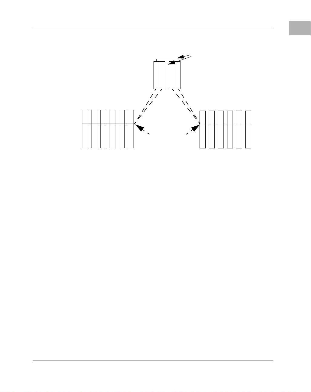
Physical Connection Process
The physical connect ion process is the basic proce ss of putting a board into
a live system, or physi cally remo ving th e board. The process i nclude s two
states:
❏ P0 - The board is physically separate from the system
❏ P1 - The board is fully seated, but not powered, and not active on
the PCI bus. All pins are connected.
Hardware Connection Process
The hardware connection pro cess involves the electrical connection or
disconnection of the board. This process includes three states:
❏ H0 - The board is not active on the PCI bus. This state is equivale nt
to P1 above.
Physical Connection Process
1
❏ H1 - The board has powered up and is suffic ie ntly initialized to
connect to the PCI bus.
❏ H2 - The board is powered, and enabled for access by a PCI bus
transaction (nor mally by the host) in PCI conf iguration space onl y .
The board configuration spa ce is not yet initialized.
When a newly inserted board has completed H2, the board is ope rable
from a hardware perspective. It has run its power up diagnostics, initi alized
itself, loaded EEPROM data, etc. The blue LED is off in the H2 state,
indicating that the board should not be pulled out.
http://www.motorola.com/computer/literature 1-17
Page 38

1
System A rchitecture
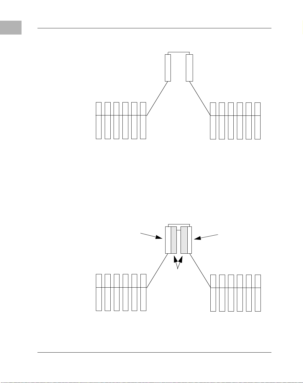
Software Con n ect io n Proce ss
The software connection process inc ludes the tasks needed to configure
and load software. This process conta ins four states:
❏ S0 - The Software Connection Process has not been initi ated. The
board’s configuration space registers are accessible but not yet
initialized.
❏ S1 - The board is configured by the system. The system has
initialized the board ’s PCI configuration space registers with I/O
space, memory space, inte rrupts a nd PCI bus nu mbers. The board
is ready to be accessed by a devic e driver, but no drivers are loaded
at this time.
❏ S2 - The necessary supporting sof tware (drivers, etc.) have been
loaded. The board is ready for use by the OS and/or the
application, but no operations involving the board are active or
pending.
❏ S3 - The board is active. Software operations are either active or
pending.
Software Disconnection Process
The software disconnecti on proce ss defines two additional states which
are used when quiescing activity on a board in prepara tion for extraction:
❏ S3Q - The software is completing current operations, but is not
allowed to start new ones . When current operations are c ompleted,
the board transitions to S2.
❏ S2Q - The board is quiesced. This is the same state as S2, except
that no new operations are allowed to be initiated.
The Software Disconnection Process proceeds as S3, S3Q, S2Q, S1, and
finally S0.
1-18 Computer Group Liter ature Center Web Site
Page 39

Typical Inserti on and E xtraction Processes
Typical Insertion and Extraction Pro cesses
Many of the steps in the inser tion and extraction proc esses are automated
by software. After the operator installs a board, it automatical ly advances
to P1. The hardware connection process proceeds automatically a nd
asserts the ENUM# signal to initi ate the softwa re conne ction process. The
host responds to the bussed ENUM# signal by reading the Hot Swap
Control Status Regist er of each board to find out which one is signaling an
insertion or extraction (INS or EXT bit asserted). Upon detecting an
insertion, the Host responds by adding software drivers to support the
newly inserted board.
Extraction is initia ted when the operator opens the board ejector handl e,
which activates a mechanica l switc h to assert ENUM#. The hot plug
system driver senses ENUM# and notifies software that board activity
must be quiesc ed and that software device drivers should be unloaded. The
application tha t is using the board is informed that the reso urce is no longer
available. When the board is ready for extraction, software informs the
operator by illuminating the blue LED. After extraction, all system
resources previously assigned to that board are made available for other
uses.
1
Device Drivers
In order to take full advantage of the high availability functions of the
CPX8216, and to support hot swap, board device drivers need to be
enhanced. Driver s need to cease a ll ac tivity whe n the devic e is a bout to be
hot swapped, and they need to support initialization of the device without
support from the device firmware or BIOS.
Further , high availability device drivers need to be able to enter a sta ndby
mode while bus control is being passed from one CPU to another. They
also provide diagnost ic interfaces for run time fault detection and for preinitialization testing of newly inserted boards.
http://www.motorola.com/computer/literature 1-19
Page 40

Overview
2CPU Modules
2
This chapter provides reference information for the CompactPCI system
controller/ host CPU modules supported in the CPX8216 system.
The correct jumper setting and pin-out information is provided for each
module.
Note The CPX750HA is som etimes identified as an MCP750HA in
some chassis and firmware documentation, for packaging and
ordering purposes, but both numbers apply to the same board.
Your system may not contain all boards listed in this chapter, or
it may contain third-par ty boards that are not listed in this
chapter. For information about third-party boards, refer to the
board manufacturer’s documentation.
This chapter contains information for the following CompactPCI boards:
Part No. Des cr iption
CPX750HA PowerPC Hot Swappable CPU 1 2-1
CPV5350 Intel H ot Swappable CPU 1 2-16
CPX750HA
The CPX750HA is a single-slot, single-board computer equipped with a
PowerPC™ 750 Series microprocesso r. The processor implements a
backside cache controller and the board comes with 1MB of cache
memory.
Table 2-1. CompactPCI Boards
Slots
Occupied Page
2-1
Page 41

CPU Modules
2
The CPX750HA offers many standard features desirable in a CompactPCI
computer system, suc h as:
❏ PCI Bridge and Interrupt Con troller
❏ ECC Memory Controller chipset
❏ 5MB to 9MB of linear FLASH memory
❏ IDE CompactFlash memory
❏ 16MB to 256MB of ECC-protected DRAM
❏ Interface to a CompactPCI bus
❏ Several I/O periph erals
The I/O peripheral interfac es present on the onboard PCI bus include:
❏ One 10/100-BASE-T Etherne t interface
❏ One USB host controller
❏ One SA master/slave interface
❏ One Fast EIDE interface
❏ One P MC Slot
Functions provided from the ISA bus are two asynchronous and two
synchronous/asynchronous serial ports, keyboard, mouse, a floppy disk
controller, printer port, a real time clock, and NVRAM.
The CPX750HA interfaces to a CompactPCI bus us ing a DEC 21 154 P CIto-PCI bridge device. This device pr ovides a 64-bit primary and a 64-bit
secondary interfa ce allo wing full 64-bit d ata ac cess between Compac tPCI
bus devices and the host/PCI bridge. This bus is capa ble of driving seven
CompactPCI slots.
Another key f eature of the CPX750HA is the P CI (Peripheral Component
Interconnect) bus. In additi on to the onboard local bus periphe rals, the PCI
bus supports an industry-standard mezzanine interface, IEEE P1386.1
PMC (PCI Mezzanine Car d). PMC m odules of fer a variety of pos sibil ities
for I/O expansion.
2-2 Computer Group Literature Center Web Site
Page 42

CPX750HA
The base board suppor ts PMC I/O for the fr ont panel or th rough backplane
connector J3 to a CPX750HATM transition module.
J6
1
3
PCI MEZZANINE CARD
10/100 BASE T
COM 1
RST
ABT
BFL
CPCI
USB 1
USB 0
CPU
CPI
J8
1
82
71
J15
69
15
J10
S2S1
189
1902
DS2
DS1 DS3
DS4
1
J17
4
1
J18
4
1
XU1
XU2
J19
2213 9804
1
2
1
2
J11
49
50
1
2
J13
49
50
J9
1902
189
J5 J4 J3 J2 J1
J12
49
50
1
2
J14
49
50
F1 F2 F3
2
http://www.motorola.com/computer/literature 2-3
Page 43

CPU Modules
2
Connectors and Ju mper Settings
The next sections provide pinout inform ation and jumper settings for the
CPX750HA board. Additiona l pinout assignments can be found in
Chapters 3 through 6.
Backplane Connectors (P5, P4, P3, P2, P1)
Refer to the backplane reference section for the backplane connector pin
assignments.
Front USB Connectors (J17 and J18)
Two USB Series A receptacl es are l oc ated at the fron t pan el of the
CPX750HA board. The pin assignments for these connec tors are as
follows:
Table 2-2. USB 0 Connector J18
1 UVCC0
2 UDATA0N
3 UDATA0P
4 GND
Table 2-3. USB 1 Connector J17
1 UVCC1
2 UDATA1N
3 UDATA1P
4 GND
10BaseT/100BaseTx Connector (J8)
The 10BaseT/100BaseTx Connector is an RJ45 connector located on the
front panel of the CPX750HA board. The pin assignments for this
connector are as follows:
2-4 Computer Group Literature Center Web Site
Page 44

Connectors and Jumper Settings
Table 2-4. 10BaseT/100BaseTx Connector J8
COM1 Connector (J15)
A standard DB9 receptac le is located on the fr ont panel of the CPX750HA
to provide the interfac e to the COM1 serial port. These COM1 signals are
also routed to J11 on the tra n sition module. A terminal may be connected
to J15 or J11 on the transition module but not both at the same time. The
pin assignments for this con nector is as follows:
2
1 TD+
2 TD-
3 RD+
4 AC Terminated
5 AC Terminated
6 RD-
7 AC Terminated
8 AC Terminated
Table 2-5. COM1 Connector J15
1 DCD
2 RXD
3 TXD
4 DTR
5 GND
6 DSR
7 RTS
8 CTS
9 RI
http://www.motorola.com/computer/literature 2-5
Page 45

CPU Modules
2
Debug Connector (J19)
A 190-pin connector (J19 on the CPX750HA base board) provid es access
to the processor bus (MPU bus) and some bridge/memory controller
signals. It can be used for debugging purposes. The pin assignments are
listed in the following table.
Table 2-6. Debug Connector (J19)
1PA0 PA1 2
3PA2 PA3 4
5PA4 PA5 6
7PA6 PA7 8
9PA8 PA9 10
11 PA10 PA11 12
13 PA12 PA13 14
15 PA14 PA15 16
17 PA16 PA17 18
19 PA18 GND PA19 20
21 PA20 PA21 22
23 PA22 PA23 24
25 PA24 PA25 26
27 PA26 PA27 28
29 PA28 PA29 30
31 PA30 PA31 32
33 PA_PAR0 PA_PAR1 34
35 PA_PAR2 PA_PAR3 36
37 APE* RSRV* 38
39 PD0 PD1 40
41 PD2 PD3 42
2-6 Computer Group Literature Center Web Site
Page 46

Connectors and Jumper Settings
Table 2-6. Debug Connector (J19) (continued)
43 PD4 PD5 44
45 PD6 PD7 46
47 PD8 PD9 48
49 PD10 PD11 50
51 PD12 PD13 52
53 PD14 PD15 54
55 PD16 PD17 56
57 PD18 +5V PD19 58
59 PA20 PD21 60
61 PD22 PD23 62
63 PD24 PD25 64
65 PD26 PD27 66
67 PD28 PD29 68
69 PD30 PD31 70
71 PD32 PD33 72
2
73 PD34 PD35 74
75 PD36 PD37 76
77 PD38 PD39 78
79 PD40 PD41 80
81 PD42 PD43 82
83 PD44 PD45 84
85 PD46 PD47 86
87 PD48 PD49 88
89 PA50 PD51 90
91 PD52 PD53 92
93 PD54 PD55 94
http://www.motorola.com/computer/literature 2-7
Page 47
CPU Modules
2
Table 2-6. Debug Connector (J19) (continued)
95 PD56 GND PD57 96
97 PD58 PD59 98
99 PD60 PD61 100
101 PD62 PD63 102
103 PDPAR0 PDPAR1 104
105 PDPAR2 PDPAR3 106
107 PDPAR4 PDPAR5 108
109 PDPAR6 PDPAR7 110
111 No Connection No Connection 112
113 DPE* DBDIS* 114
115 TT0 TSIZ0 116
117 TT1 TSIZ1 118
119 TT2 TSIZ2 120
121 TT3 No Connection 122
123 TT4 No Connection 124
125 CI* No Connection 126
127 WT* No Connection 128
129 GLOBAL* No Connection 130
131 SHARED* DBWO* 132
133 AACK* +3.3V TS* 134
135 ARTY* XATS* 136
137 DRTY* TBST* 138
139 TA* No Connection 140
141 TEA* No Connect ion 142
143 No Connection DBG* 144
145 No Connection DBB* 146
2-8 Computer Group Literature Center Web Site
Page 48

Connectors and Jumper Settings
Table 2-6. Debug Connector (J19) (continued)
147 No Connection ABB* 148
149 TCLK_OUT MPUBG-0* 150
151 No Connection MPUBR0* 152
153 MPUBR1* IRQ0* 154
155 MPUBG1* MCHK* 156
157 WDT1TO* SMI* 158
159 WDT2TO* CKSTPI* 160
161 L2BR* CKSTPO* 162
163 L2BG* HALTED (N/C) 164
165 CLAIM* TLBISYNC* 166
167 No Connection TBEN 168
169 No Connection* No Connection 170
171 No Connection* GND No Connection 172
173 No Connection* No Connection 174
175 No Connection NAPRUN 176
2
177 SRST1* QREQ* 178
179 SRESET* QAC K* 180
181 HRESET* CPUTDO 182
183 GND CPUTDI 184
185 CPUCLK1 CPUTCK 186
187 No Connection CPUTMS 188
189 No Connection CPUTRST* 190
http://www.motorola.com/computer/literature 2-9
Page 49

CPU Modules
2
DRAM Mezzanine Connector (J10)
A 190-pin connector (J10 on the CPX750HA base board) supplies the
interface b etw een the mem o ry bus and the RAM300 DRAM mezzanine.
The pin assignments are listed in the following table.
Table 2-7. DRAM Mezzanine Connector (J10)
1A_RAS∗ A_CAS∗ 2
3B_RAS∗ B_CAS∗ 4
5C_RAS∗ C_CAS∗ 6
7D_RAS∗ D_CAS∗ 8
9OEL∗ OEU∗ 10
11 WEL∗ WEU∗ 12
13 ROMACS∗ ROMBCS∗ 14
15 RAMAEN RAMBEN 16
17 RAMCEN EN5VPWR 18
19 RAL 0 GND RAL1 20
21 RAL 2 RAL3 22
23 RAL 4 RAL5 24
25 RAL 6 RAL7 26
27 RAL 8 RAL9 28
29 RAL 10 RAL11 30
31 RAL 12 RAU0 32
33 R AU1 RAU2 34
35 R AU3 RAU4 36
37 R AU5 RAU6 38
39 R AU7 RAU8 40
41 R AU9 RAU10 42
43 R AU11 RAU12 44
2-10 Computer Group Liter ature Center Web Site
Page 50

Connectors and Jumper Settings
Table 2-7. DRAM Mezzanine Connector (J10) (continued)
45 RDL0 RDL1 46
47 RDL2 RDL3 48
49 RDL4 RDL5 50
51 RDL6 RDL7 52
53 RDL8 RDL9 54
55 RDL10 RDL11 56
57RDL12+5VRDL1358
59 RDL14 RDL15 60
61 RDL16 RDL17 62
63 RDL18 RDL19 64
65 RDL20 RDL21 66
67 RDL22 RDL23 68
69 RDL24 RDL25 70
71 RDL26 RDL27 72
73 RDL28 RDL29 74
2
75 RDL30 RDL31 76
77 RDL32 RDL33 78
79 RDL34 RDL35 80
81 RDL36 RDL37 82
83 RDL38 RDL39 84
85 RDL40 RDL41 86
87 RDL42 RDL43 88
89 RDL44 RDL45 90
91 RDL46 RDL47 92
93 RDL48 RDL49 94
95 RDL50 GND RDL51 96
http://www.motorola.com/computer/literature 2-11
Page 51

CPU Modules
2
Table 2-7. DRAM Mezzanine Connector (J10) (continued)
97 RDL 52 RDL53 98
99 RDL 54 RDL55 100
101 RDL56 RDL57 102
103 RDL58 RDL59 104
105 RDL60 RDL61 106
107 RDL62 RDL63 108
109 CDL0 CDL1 110
111 CDL2 CDL3 112
113 CDL4 CDL5 114
115 CDL6 CDL7 116
117 No Connection No Connection 118
119 RDU0 RDU1 120
121 RDU2 RDU3 122
123 RDU4 RDU5 124
125 RDU6 RDU7 126
127 RDU8 RDU9 128
129 RDU10 RDU11 130
131 RDU12 RDU13 132
133 RDU14 +3.3V RDU15 134
135 RDU16 RDU17 136
137 RDU18 RDU19 138
139 RDU20 RDU21 140
141 RDU22 RDU23 142
143 RDU24 RDU25 144
145 RDU26 RDU27 146
147 RDU28 RDU29 148
2-12 Computer Group Liter ature Center Web Site
Page 52

Connectors and Jumper Settings
Table 2-7. DRAM Mezzanine Connector (J10) (continued)
149 RDU30 RDU31 150
151 RDU32 RDU33 152
153 RDU34 RDU35 154
155 RDU36 RDU37 156
157 RDU38 RDU39 158
159 RDU40 RDU41 160
161 RDU42 RDU43 162
163 RDU44 RDU45 164
165 RDU46 RDU47 166
167 RDU48 RDU49 168
169 RDU50 RDU51 170
171 RDU52 GND RDU53 172
173 RDU54 RDU55 174
175 RDU56 RDU57 176
177 RDU58 RDU59 178
2
179 RDU60 RDU61 180
181 RDU62 RDU63 182
183 CDU0 CDU1 184
185 CDU2 CDU3 186
187 CDU4 CDU5 188
189 CDU6 CDU7 190
http://www.motorola.com/computer/literature 2-13
Page 53

CPU Modules
2
EIDE Compact FLASH Connector (J9)
A 50-pin Compact F LASH card header connector provides the EIDE
interface to the Compact FLASH Memory Card. The pin assignments for
this connector are as follows:
Table 2-8. EIDE Compact FLASH Connector J9
1 GND DATA3 2
3 DATA4 DATA5 4
5 DATA6 DATA7 6
7 DCS1A_L GND 8
9 GND GND 10
11 GND GND 12
13 +5V GND 14
15 GND GND 16
17 GND DA2 18
19 DA1 DA0 20
21 DATA0 DATA1 22
23 DATA2 NO CONNECT 24
25 CD2_L CD1_L 26
27 DATA11 DATA12 28
29 DATA13 DATA14 30
31 DATA15 DCS3A_L 32
33 NO CONNECT DIORA_L 34
35 DIOWA_L NO CONNECT 36
37 INTRQA +5V 38
39 MASTER/ SLAVE NO CONNECT 40
41 RS T_L DIORDYA 42
43 NO CONNECT NO CONNECT 44
2-14 Computer Group Liter ature Center Web Site
Page 54

Connectors and Jumper Settings
Table 2-8. EIDE Compact FLASH Connector J9
45 NO CONNECT NO CONNECT 46
47 DATA8 DATA9 48
49 DATA10 GND 50
Flash Bank Selection (J6)
The CPX750HA base board has provision for 1MB of 16-bit flash
memory. The RAM300 memory mezzanine accommodates 4MB or 8MB
of additional 64-bit flash m emory.
The flash memory is organized in eithe r one or two banks, each bank either
16- or 64-bits wide. Bank B contains the onboard de bugger, PPCBug.
T o en able fla sh ban k A (4MB or 8MB of fir mware reside nt on soldere d-in
devices on the RAM300 mezza nine) , pla ce a j umper acros s he ader J 6 pi ns
1 and 2. To enable fla sh ban k B (1MB of firmware lo cated in soc k et s on
the base board), place a jumper across he ader J6 pins 2 and 3.
2
J6J6
3
3
2
1
Flash Bank A Enabled (4MB/8MB, Soldered) Flash Bank B Enabled (1MB, Sockets)
2
1
(Factory Configuration)
http://www.motorola.com/computer/literature 2-15
Page 55

CPU Modules
2
CPV5350
The CPV5350 Single Boar d Computer (SBC) is a hot swap, CompactPCI
(Compact Peripheral Communication Interface) compliant computer with
high availability pla tform support. It is powered by a PICMG (PCI
Industrial Computer Manufacturers Group) compatible Pentium® II
Deschutes Mobile Module. The CPV5350’s 6U CompactPCI standard
form factor (160mm x 233mm x 61mm), 4HP (.8 inch) is designed for
installation into PICMG CompactPCI-compliant backplanes.
The CPV5350 provides:
❏ Standard PC I/O
❏ USB
❏ PCI EIDE
❏ 3D AGP graphics
❏ Dual fast Ethernet controllers
❏ Optional onboard CompactF lash™ connector
The CPV5350’s front panel has connectors for:
❏ Keyboard/mouse
❏ Video
❏ Two serial ports (COM1 and COM2)
❏ Two Ethernet ports
❏ Two USB ports
❏ LED Indicator lights for wat chdog alarm, speaker st atus, ha rd disk
drive activity, and power.
Refer to the following ill ustra tion for front panel c onnector s and LEDs on
the CPV5350.
2-16 Computer Group Liter ature Center Web Site
Page 56

Video
COM 1
Ethernet 1
Ethernet 2
USB
CPV5350
2
V
I
D
E
O
1
COM 2
2
1
E
T
H
E
R
N
E
T
2
Keyboard/Mous e
RESET
Indicator
Lights
RESET
SPKR
ALRM
PWR
HDD
CPV5350
http://www.motorola.com/computer/literature 2-17
Page 57

CPU Modules
2
Connectors
The next table lists the connectors available to support devices on the
CPV5350. Figure 2-1 on page 2-19 shows the location of the connectors
described in the table.
Table 2-9. CPV5350 Front Panel Connectors, Board
Headers and Componen ts
Connector Description
J1 Backplane connecto r
J2 Backplane connecto r
J3 Backplane connecto r
J4 Backplane connecto r
J5 Backplane connecto r
J6 E therne t 2
J9 E IDE
J10 Reserved (in-circuit programming)
J12 Reserved (in-circuit emulator)
J13 Eth ernet 1
J14 USB port 1
J16 Reset (c onnected to push-butt on on the front panel)
J21 Flash ROM
J23 Video connector
J24 CO M 1 (S erial P o r t 1)
J25 CO M 2 (S erial P o r t 2)
J50 Keyboard/Mouse
2-18 Computer Group Liter ature Center Web Site
Page 58

Transiti on Module
2
U34 U35
U30 U31
12
J12
J5
U11
J23
J4
J24 J25
J3
2475 99012475 9901
J13 J6
2
1
BT1
T1 T2
J2
U38
J20
U55
U62
J14 J50
J1
U50
U25 U26
J51
CR2 CR4
21
CRI
8
J17
1
J21
CR3
Figure 2-1. CPV5350 Component Side View
Transitio n Mo du le
The CPV5350TM80 transi tion module provides backpl ane I/O through the
J3 and J5 connectors on the CPV5350 controll er modul e.
When the identical function is available through the CPV5350’s front
panel and the rear transition module, you can use either the front or the
rear , not both.
http://www.motorola.com/computer/literature 2-19
Page 59

CPU Modules
2
DRAM Memory Configuration
The CPV5350 has one 168-pin DIMM site for memory expansion. The
DIMM sites accept industry standar d PC100-com pliant DIMM modules
(8, 16, 32, 64, 128, or 256MB) with or without ECC. You can use either
registered or unbuffered memory modules.
Keyboard/Mouse PS2 Connector
The keyboard/mouse connector (J50) uses a 6-pin, female PS/2 c onnector.
Table 2-10. Keyboard/Mouse P/S2 Connector Pin
Assignments (J50)
Pin
Number
1 KBDDAT Keyboard Data
2 AUXDAT Auxiliary Data
3 GND Ground
4 KBDVCC Keyboard Power (c urrent limited to .75 Amp)
5 KBDCLK Keyboard Clock
Signal
Mnemonic Si gn al Des cription
6 AUXC LK Auxiliary Clock
7 CGND Common Ground
6
4
2
2489 9902
5
3
1
7
Figure 2-2. Keybo ar d/M ous e Conne cto r Diagra m
2-20 Computer Group Liter ature Center Web Site
Page 60

Ethernet Connectors
Ethernet Connec tors
Ethernet 1 (J13) and Ethernet 2 (J6) use standard RJ-45 connectors.
T able 2-11. Etherne t Connec tor P in Ass ignme nt s (J13 an d
J6)
Pin
Num ber Signa l M n emon ic Si gnal De s c r i p t io n
1 TX+ Differential transmit lines
2 TX- Differential transmit lines
3 RX+ Differential receive lines
4-- -5-- -6 RX- Differential receive lines
7-- -8-- --
Univ ersal Serial Bus (USB) Connector
2
USB Port 1 and Port 2 (J14) use a 2 x 4 pin USB connector.
Table 2-12. USB Connector Pin Assignments (J14)
Pin
Number Signal Mnemonic Signal Description
1 +5V Current limited USB power
2 DATA+ USB serial communication diffe rential
3 DATA- USB serial communication differenti al
4 GND USB port common
http://www.motorola.com/computer/literature 2-21
Page 61

CPU Modules
2
Serial Port Connectors
COM 1 (Serial Port 1) (J2 4) an d COM 2 (Seria l Port 2) (J25) use 2 x 9-pin
D-sub connectors.
Table 2-13. Serial Port Connector Pin Assignments (J24
and J25)
Pin
Number
1 DCD- dat a set has detected the d ata carrier
2 RX Receives serial data input from communication
3 TX S ends serial output to communication link
4 DTR- data s et is ready to establish a communication link
5 GND Ground
6 DSR- data set is ready to establish a comm unication link
7 RTS- indicates to data set that UART is ready to
8 CTS- data set is ready to exchan ge data
Signal
Mnemonic Signal Description
link
exchange data
9 RI- modem has received a telephone ring ing signal
Video Connector
The video connector (J23) uses a 15-pin high de nsity D-sub connector.
Table 2-14. Video Connector Pin Assignments (J23)
Pin
Number Signal Mnemonic Signal Descrip tion
1 RED Red signal
2 GREEN Green signal
3 BLUE Blue signal
2-22 Computer Group Liter ature Center Web Site
Page 62

Video Connector
Table 2-14. Video Connector Pin Assignments (J23)
Pin
Number Signal Mnemonic Signal Description
4 NC Not connected
5 DACVSS Video return
6 DACVSS Video return
7 DACVSS Video return
8 DACVSS Video return
9 NC Not connected
10 DACVSS Video return
11 NC Not connected
12 DDCDAT Display data channel data signal for
DDC2 support
13 HSYNC Horizontal synchronization
14 VSYNC Ve rtical synchronization
15 DDCCLK Display data channel clock signal for
DDC2 support
2
http://www.motorola.com/computer/literature 2-23
Page 63

3CPX8540 Carrier Card
Overview
This chapter provid es reference information for the CPX8540 carrier card.
The CPV8540 is a 64-bit, 6U, single-width ( 4HP) CompactPCI® card tha t
provides front access to PMC modules with both front and rear I/O
connectivity. Rear I/O co nne ct ions via J3 and J5 allow its use in both
standard CompactPCI backpl anes a nd CompactPCI backplanes with the
H.110 CT bus. The corr ect jum per settings and pin-out information is
provided for each connect or on the carrie r card.
This chapter does not include the system controller/host modules. For
information about the system controller/host, refer to Chapter 2, CPU
Modules.
CPX8540 Carrier Card
3
The CPX8540 carrier card provides connectivity to a wide variety of
video, ATM, analog, serial, and many other funct ions. The board suppor ts
one double-width or two single- width PMC mezzanine modules.
Once connected, the PMC modules are accessed via front panel
connections of the carrie r card. In addition, I/O lines are brought out to the
carrier card’s rear 2mm pin and socket connectors, allowing rear panel
connections in systems such as the CPX8216T chassis.
Key features of the CPX8540 are:
❏ Supports standard (IEEEP1386.1) PMC mezzanine modules
❏ Holds one double-width or two single-width modules
❏ All PMC I/O brought out to the front panel and to rear connectors
❏ Single CompactPCI loa d via DEC 21154 bridge
❏ Supports 5.0 or 3.3 Volt PMC modules
❏ Supports Plug and Pla y
3-1
Page 64

CPX8540 Carrier Car d
The CPX8540 reports itself to the system as a bridge c hip with the PMC
functions behind it.
The following two figures provide ove rvi ews of the card.
3
J5
PMC2
J3
PMC1
J2
Bridge
J1
Figure 3-1. PMC Modules to CPX8540 Carrier Card
3-2 Computer Group Literature Center Web Site
Page 65

CPX8540 Carrier Card
3
J21
J23
J11
J13
J22
J24
J12
J14
Single Width
PMC Module
Figure 3-2. Installing a PMC Module
http://www.motorola.com/computer/literature 3-3
Page 66

CPX8540 Carrier Car d
Connector Pinouts
The tables in this sectio n provide the connector pinout information f or the
3
14 +3.3V +3.3V +3.3V +5V +5V 14
13 PMC1IO5 PMC1IO4 PMC1IO3 PMC1IO2 PMC1IO1 13
12 PMC1IO10 PMC1IO9 PMC1IO8 PMC1IO7 PMC1IO6 12
11 PMC1IO15 PMC1IO14 PMC1IO13 PMC1IO12 PMC1IO11 11
10 PMC1IO20 PMC1IO19 PMC1IO18 PMC1IO17 PMC1IO16 10
9 PMC1IO25 PMC1IO24 PMC1IO23 PMC1IO22 PMC1IO21 9
8 PMC1IO30 PMC1IO29 PMC1IO28 PMC1IO27 PMC1IO26 8
7 PMC1IO35 PMC1IO34 PMC1IO33 PMC1IO32 PMC1IO31 7
rear connectors on the carrier card.
Table 3-1. CPCI J3 I/O Connector Pinout
ROW A ROW B ROW C ROW D ROW E
6 PMC1IO40 PMC1IO39 PMC1IO38 PMC1IO37 PMC1IO36 6
5 PMC1IO45 PMC1IO44 PMC1IO43 PMC1IO42 PMC1IO41 5
4 PMC1IO50 PMC1IO49 PMC1IO48 PMC1IO47 PMC1IO46 4
3 PMC1IO55 PMC1IO54 PMC1IO53 PMC1IO52 PMC1IO51 3
2 PMC1IO60 PMC1IO59 PMC1IO58 PMC1IO57 PMC1IO56 2
1 V(I/O) PMC1IO64 PMC1IO63 PMC1IO62 PMC1IO61 1
NOTE: PMC1IO* signal s are those connected to the lower PMC slot, or slot 1.
Table 3-2. CPCI J5 I/O Connector Pinout
ROW A ROW B ROW C ROW D ROW E
13 PMC2IO5 PMC2IO4 PMC2IO3 PMC2IO2 PMC2IO1 13
12 PMC2IO10 PMC2IO9 PMC2IO8 PMC2IO7 PMC2IO6 12
11 PMC2IO15 PMC2IO14 PMC2IO13 PMC2IO12 PMC2IO11 11
3-4 Computer Group Literature Center Web Site
Page 67

Conn ecto r P inou t s
Table 3-2. CPCI J5 I/O Connector Pinout (continued)
10 PMC2IO20 PMC2IO19 PMC2IO18 PMC2IO17 PMC2IO16 10
9 PMC2IO25 PMC2IO24 PMC2IO23 PMC2IO22 PMC2IO21 9
8 PMC2IO30 PMC2IO29 PMC2IO28 PMC2IO27 PMC2IO26 8
7 PMC2IO35 PMC2IO34 PMC2IO33 PMC2IO32 PMC2IO31 7
6 PMC2IO40 PMC2IO39 PMC2IO38 PMC2IO37 PMC2IO36 6
5 PMC2IO45 PMC2IO44 PMC2IO43 PMC2IO42 PMC2IO41 5
4 PMC2IO50 PMC2IO49 PMC2IO48 PMC2IO47 PMC2IO46 4
3 PMC2IO55 PMC2IO54 PMC2IO53 PMC2IO52 PMC2IO51 3
2 PMC2IO60 PMC2IO59 PMC2IO58 PMC2IO57 PMC2IO56 2
1 V(I/O) PMC2IO64 PMC2IO63 PMC2IO62 PMC2IO61 1
NOTE: PMC2IO* signals are those connected to the upper PMC slot, or slot 2.
Table 3-3. PCI 32-bit Interface Connector P11/J11, P21/J21
Pin# Signal Name Signal Name Pin #
1 TCK -12V 2
3 GND INTA# 4
5INTB# INTC# 6
7 BUSMODE1# +5V 8
3
9 INTD# PC I-RSVD* 10
11 GND PCI-RSVD* 12
13 CLK GND 14
15 GND GNT# 16
17 REQ# +5V 18
19 V (I/O) AD[31] 20
21 AD[28] AD[27] 22
23 AD[25] GND 24
http://www.motorola.com/computer/literature 3-5
Page 68

CPX8540 Carrier Car d
Table 3-3. PCI 32-bit Interface Connector P11/J11, P21/J21 (continued)
Pin# Signal Name Signal Name Pin #
3
25 GND C/BE[3]# 26
27 AD[22] AD[21] 28
29 AD[19] +5V 30
31 V (I/O) AD[17] 32
33 FRAME# GND 34
35 GND IRDY# 36
37 DEVSEL# +5V 38
39 GND LOCK# 40
41 SDONE# SBO# 42
43 PAR GND 44
45 V (I/O) AD[15] 46
47 AD[12] AD[11] 48
49 AD[09] +5V 50
51 GND C/BE[0]# 52
53 AD[06] AD[05] 54
55 AD[04] GND 56
57 V (I/O) AD[03] 58
59 AD[02] AD[01] 60
61 AD[00] +5V 62
63 GND REQ64# 64
3-6 Computer Group Literature Center Web Site
Page 69

Conn ecto r P inou t s
Table 3-4. PCI 32-bit Interface Connector P12/J12, P22/J22
Pin# Signal Name Signal Name Pin #
1+12V TRST# 2
3TMS TDO 4
5 TDI GND 6
7 GND PCI-RSVD* 8
9 PCI-RSVD* PCI-RSVD* 10
11 BUSMODE2# +3.3V 12
13 RST# BUSMODE3# 14
15 +3.3V BUSMODE4# 16
17 PCI-RSVD* GND 18
19 AD[30] AD[29] 20
21 GND AD[26] 22
23 AD[24] +3.3V 24
25 IDSEL AD[23] 26
27 +3.3V AD[20] 28
29 AD[18] GND 30
31 AD[16] C/BE[2]# 32
33 GND PMC -RSVD 34
3
35 TRDY# +3.3V 36
37 GND STOP# 38
39 PERR# GND 40
41 +3.3V SERR# 42
43 C/BE[1]# GND 44
45 AD[14] AD[13] 46
47 GND AD[10] 48
49 AD[08] +3.3V 50
http://www.motorola.com/computer/literature 3-7
Page 70

CPX8540 Carrier Car d
Table 3-4. PCI 32-bit Inter fac e Con nec tor P12/J12, P22/J22 (continued)
Pin# Signal Name Signal Name Pin #
3
51 AD[07] PMC-RSVD 52
53 +3.3V PMC-RSVD 54
55 PMC-RSVD GND 56
57 PMC-RSVD PMC-RSVD 58
59 GND PMC -RSVD 60
61 ACK64# +3.3V 62
63 GND PMC -RSVD 64
Table 3-5. PCI 64 bit PCI extension on PMC Connector J13, J23
Pin# Signal Name Signal Name Pin #
1 - GND 2
3 GND C/BE7# 4
5 C/BE6# C/BE5# 6
7 C/BE4# GND 8
9 V(I/O) PAR64 10
11 AD63 AD62 12
13 AD61 GND 14
15 GND AD60 16
17 AD59 AD58 18
19 AD57 GND 20
21 V(I/O) AD56 22
23 AD55 AD54 24
25 AD53 GND 26
27 GND AD52 28
29 AD51 AD50 30
3-8 Computer Group Literature Center Web Site
Page 71
Conn ecto r P inou t s
Table 3-5. PCI 64 bit PCI extension on PMC Connector J13, J23
Pin# Signal Name Signal Name Pin #
31 AD49 GND 32
33 GND AD48 34
35 AD47 AD46 36
37 AD45 GND 38
39 V(I/O) AD44 40
41 AD43 AD42 42
43 AD41 GND 44
45 GND AD40 46
47 AD39 AD38 48
49 AD37 GND 50
51 GND AD36 52
53 AD35 AD34 54
55 AD33 GND 56
57 V(I/O) AD32 58
59--60
61 - GND 62
63 GND - 64
3
Table 3-6. User-Defined I/O PCI Interface Connector P14/J14 , P24/J 24
Pin# Signal Name
1-64 I/O
http://www.motorola.com/computer/literature 3-9
Page 72

Overview
This chapter provides reference information for the PMC module
supported in the CPX8216 system.
SCSI-2 Controller PMC
The SCSI-2 controller provide s fast and wide, single-ended, SCSI-2
(Small Computer System Interface-2) high throughput connectivity for
host carrier boards equipped with PMC (PCI Mezzanine Card)
connections.
The PMC adapter is a plug-and-play device with systems that are
compliant with the PCI Local Bus Specification (revision 2.0).
This controller has the following capabilities:
4PMC Modules
4
❏ Single-wide PMC module
❏ 32-bit wide PCI bus support
❏ 128Kb onboard flas h memory
❏ 20 Mbps Fast and W ide SCSI-2
❏ Single-ended SCSI-2 interfaces
❏ Front and rear User I/ O
❏ 68-pin front panel connector
❏ 64-pin JN4/P N4 rear connector
❏ +3.3V and +5V signaling
❏ Compliance to PCI local bus specification (Revision 2.0)
4-1
Page 73

PMC Modules
The following figure shows the PMC150 component layout a nd front
panel.
PN4
PN2
4
PN1
U5
U31
JP40
U1
U13U14U15
S1
4118 0702
4-2 Computer Group Literature Center Web Site
Page 74

Switch Settings
Use this table as a guideline for configuring the 6-position dip switch on
your PMC.
Switch On Function Off Function Default
1 Use INTA No Use INTA On
2 Use INTB No Use INTB Off
3 Use INTC No Use INTC Off
4 Use INTD No Use INTD Off
5 TERM Enable TERM Disable On
6 Little Endian Big Endian On
Configure the Big/Litt le endian mode to your ap propriate appli cation for pr oper
software operation.
Make sure only one INTx line switch is in the ON position.
Enable TERM ENAB is On only if this SCSI controlle r is physically at the end
of the SCSI bus. If the SCSI controller is in a ny other pos ition on the bus, TERM
ENAB must be in the OFF mode.
Switch Settings
Table 4-1. PMC Switch Settings
4
T erminators - The SCSI bus (cable) must be properly term inated at each
end of the bus. The first and last device on the bus should be the only
devices that are set to termina te the bus.
T erminator Power - The SCSI terminators requir e adequate voltage to
properly te rminate t he SCSI bus. All SCSI host a dapter s o n the bus should
be set to supply terminator power; and where possible, be located at the
end of the bus and serve as bus terminators. The terminator resistors must
be present on the first and last devi ce on the bus only.
For further informa tion on this PMC, vis it the T e chnobox, Inc . we b site at
http://www.technobox.com.
http://www.motorola.com/computer/literature 4-3
Page 75

PMC Modules
Connector Pin Assignments
The table below provides the connector pin assignments for the SCSI
connector on the PMC adapter. The connector uses a 68-pin Euro-style
SCSI cable, either shielded for external or interna l cabinet applications or
non-shielded for interna l cabinet applications only. For rear I/O, a 64-pin
4
conductor cable is used. The pin assignmen ts are also provided in the
following table.
Table 4-2. PMC Pin Assignments
64-Pin
Signal
name
68-Pin
Connector
Number
Conductor
Cable
Number
68-Pin
Connector
Number
Signal
name
Ground
Ground
Ground
Ground
Ground
Ground
Ground
Ground
Ground
Ground
Ground
Ground
Ground
Ground
Ground
Ground
TERMPWR
TERMPWR
Reserved
Ground
Ground
Ground
Ground
1
2
3
4
5
6
7
8
9
10
11
12
13
14
15
16
17
18
19
20
21
22
23
1
3
5
7
9
11
13
15
17
19
21
23
25
27
29
31
33
N/C
N/C
35
37
39
41
2
4
6
8
10
12
14
16
18
20
22
24
26
28
30
32
34
N/C
N/C
36
38
40
42
35
36
37
38
39
40
41
42
43
44
45
46
47
48
49
50
51
52
53
54
55
56
57
-DB(12)
-DB(13)
-DB(14)
-DB(15)
-DB(P1)
-DB(0)
-DB(1)
-DB(2)
-DB(3)
-DB(4)
-DB(5)
-DB(6)
-DB(7)
-DB(P)
Ground
Ground
TERMPWR
TERMPWR
Reserved
Ground
-ATN
Ground
-BSY
4-4 Computer Group Literature Center Web Site
Page 76

Connector Pin Assignments
Table 4-2. PMC Pin Assignments (continued)
64-Pin
Signal
name
68-Pin
Connector
Number
Conductor
Cable
Number
68-Pin
Connector
Number
Signal
name
Ground
Ground
Ground
Ground
Ground
Ground
Ground
Ground
Ground
Ground
Ground
24
25
26
27
28
29
30
31
32
33
34
43
45
47
49
51
53
55
57
59
61
63
44
46
48
50
52
54
56
58
60
62
64
58
59
60
61
62
63
64
65
66
67
68
-ACK
-RST
-MSG
-SEL
-C/D
-REQ
-I/O
-DB(8)
-DB(9)
-DB(10)
-DB(11)
4
http://www.motorola.com/computer/literature 4-5
Page 77

5Transition/Bridge Modules
Overview
5
This chapter provides reference information for the various transition and
bridge modules supported in the CPX8216 system.
The correct jumper setting and pin-out information is provided for each
module.
Note The CPX750HATM is also used with the MCP750HA in some
chassis configurations.
Your system may not contain all boards listed in this chapter, or
it may contain third-par ty boards that are not listed in this
chapter. For information about third-party boards, refer to the
board manufacturer’s documentation.
The following table lists the modules covered in this chapter:
Table 5-1. System Components
Topic: Page:
CPX750HATM Transition Module 5-1
CPV5350TM80 Transition Module 5-29
CPX750HATM Transition Module
The CPX750HATM transition module provides the interface between the
standard Paralle l Port, EIDE port, floppy port, keyboar d/mouse port, Seria l
Port connector s, and the CPX750HA CompactP CI Single Board Computer
module.
5-1
Page 78

Transition/Bridge Modules
The CPX750HATM transition module includes:
❏ Industry-sta ndard connectors for these inte rfa ces:
– Two asynchronous RJ-45 serial ports (DTE)
– Two asynchronous/synchronous HD-26 serial ports, label ed
Serial 3 and Serial 4 on t he face plate, whic h can be configured
for EIA-232-D, EIA-530, V.35, or X.21 interfaces (DCE or
DTE) through the installation of Motorola ’s Serial Interface
5
❏ Two 60-pin Serial Interface Module (SIM) connectors for
❏ One 40-pin header for EIDE port
❏ One 34-pin header for floppy por t
❏ Two 64-pin headers for PMCIO (1 gr ound pi n provided wi th ea ch
Modules (SIMs)
– One parallel port (IEEE Standard 1284-I compliant)
– One combination keyboard/mouse port
configuring the asynchronous/synchronous serial port s
PMCIO signal)
Figure 5-1 on page 5-3 shows the CPX750HATM transition module
component layout and the front panel. See Co nnectors on page 5-4 for a
list of the front panel por t connectors.
Serial Ports 3 and 4 Defaul t Configuratio n
The CPX750HATM serial ports 3 and 4 are factory configured as follows:
❏ Serial Port 3: DTE (with SIMM 01-W3877B01A insta lled)
❏ Serial Port 4: DCE (with SIMM 01-W3876B01A installed)
5-2 Computer Group Literature Center Web Site
Page 79

Serial Ports 3 and 4 Default Configuration
2214 98 04
34
33
40
39
41
J19
USB 0
J17
J15
2
1
2
J4
J8
J9 J13
J3 J5
64
J21
2
1
2
1
3
1
3
1
63
64
1
2
J14
63
J2
1
41
J18
J16
82
71
J11
82
71
J10
J7
59
60
J23
1
2
60
59
J1
1
2
17 1
34 18
J6
13 1
26 14
J24
13 1
26 14
USB 1
KB/MS
COM 1
COM 2
SERIAL 3PARALLEL
SERIAL 4
5
Figure 5-1. CPX750HATM Transition Module
http://www.motorola.com/computer/literature 5-3
Page 80

Transition/Bridge Modules
Serial Port Interface Jumper (J8 and J9)
J8 (for serial port 3) and J9 (for serial port 4) set the serial ports to either
DTE or DCE communication. For more inf ormation a bout configurin g the
serial port, se e Installing the Serial Interface Modules on page 5-16.
5
123 123
DTE
DCE
11650 9610
Figure 5-2. Serial Port Interface Jum per (J9) Settin gs
Connect ors
Refer to Figure 5-1 on page 5-3 for the location of the following conne ctors
Backplane Connectors (J3/J4/J5)
I/O signals and power are provided to the CPX750HATM from the
CPX750 through CompactPCI connectors J3 and J5. The J4 connect or is
for physical alignment purposes only and has no functional pin
connections or assignments.
Connector J3 is a 95- pin AMP Z-pac k 2mm har d metric typ e B conne ctor.
This connector route s the I/O signa ls for t he PMC I/O a nd ser ial cha nnels.
The pin assignments for J3 are as follows (outer row F is assigned and used
as ground pins but is not shown in the table):
Connector J4 is a 110-p in 2mm hard metri c type A connect or. This
connector is pl aced on the board for alignment purposes only . The keying
tabs on the type A connect or assist with al ignment of pins in t he backplane
connector during insertion of the boards. No signals are connected to J4
except the row F ground pins.
Connector J5 is a 110 -pin AMP Z-pack 2mm hard metric type B connector .
This connector routes the I/O signals for the IDE (secondary port), the
keyboard, the mouse, the two USB ports, and the printer ports. The pin
5-4 Computer Group Literature Center Web Site
Page 81

Connectors
assignments for J5 are as follows ( the outer row F is assigned and used as
ground pins but is not shown in the table):
T able 5-2 and T abl e 5-3 provide the pin assi gnments and signal mnemonic s
for connectors J3 and J5 (J4 is not shown)
Table 5-2. J3 User I/O Connector
ROW A ROW B ROW C ROW D ROW E
19 Reserved +12V -12V RXD3 RXD4 19
18 Reserved GND RXC3 GND RXC4 18
17 Reserved MXCLK MXDI MXSYNC_L MXDO 17
16 Reserved GND TXC3 GND TXC4 16
15 Reserved Reserved Reserved TXD3 TXD4 15
14 +3.3V +3.3V +3.3V +5V +5V 14
13 PMCIO5 PMCIO4 PMCIO3 PMCIO2 PMCIO1 13
12 PMCIO10 PMCIO9 PMCIO8 PMCIO7 PMCIO6 12
5
11 PMCIO15 PMCIO14 PMCIO13 PMCIO12 PMCIO11 11
10 PMCIO20 P MCIO19 PMC IO18 PMCIO17 PMCIO16 10
9 PMCIO25 PMCIO24 PMCIO23 PMCIO22 PMCIO21 9
8 PMCIO30 PMCIO29 PMCIO28 PMCIO27 PMCIO26 8
7 PMCIO35 PMCIO34 PMCIO33 PMCIO32 PMCIO31 7
6 PMCIO40 PMCIO39 PMCIO38 PMCIO37 PMCIO36 6
5 PMCIO45 PMCIO44 PMCIO43 PMCIO42 PMCIO41 5
4 PMCIO50 PMCIO49 PMCIO48 PMCIO47 PMCIO46 4
3 PMCIO55 PMCIO54 PMCIO53 PMCIO52 PMCIO51 3
2 PMCIO60 PMCIO59 PMCIO58 PMCIO57 PMCIO56 2
1 VIO PMCIO64 PMCIO63 PMCIO62 PMCIO61 1
Row F is assigned and used as ground pins but is not shown in the table
http://www.motorola.com/computer/literature 5-5
Page 82

Transition/Bridge Modules
Table 5-3. J5 User I/O Connector
ROW A ROW B ROW C ROW D ROW E
22 Reserved GND Reserved +5V SPKROC_L 22
21 KBDDAT KBDCLK KB AUXVCC AUXDAT AUXCLK 21
20 Reserved Reserved Reserved GND Reserved 20
19 STB_L GND UVCC0 Reserved Reserved 19
5
18 AFD_L Reserved Reserved GND UVCC1 18
17 PD2 INIT_L PD1 ERR_L PD0 17
16 PD6 PD5 PD4 PD3 SLIN_L 16
15 SLCT PE BUSY ACK_L PD7 15
14 RTSa CTSa RIa GND DTRa 14
13 DCDa +5V RXDa DSRa TXDa 13
12 RTSb CTSb RIb +5V DTRb 12
11 DCDb GND RXDb DSRb TXDb 11
10 TR0_L WPROT_L RDATA_L HDSEL_L DSKCHG_L 10
9 MTR1_L DIR_L STEP_L WDATA_L WGATE_L 9
8 Reserved INDEX_L MTR0_L DS1_L DS0_L 8
7 CS1FX_L CS3FX_L DA1 Reserved Reserved 7
6 Reserved GND Reserved DA0 DA2 6
5 DMARQ IORDY DIOW_L DMACK_L DIOR_L 5
4 DD14 DD0 GND DD15 INTRQ 4
3 DD3 DD12 DD2 DD13 DD1 3
2 DD9 DD5 DD10 DD4 DD11 2
1 RESET_L DRESET_L DD7 DD8 DD6 1
Row F is assigned and us ed as ground pins but is not shown in the table
Asynchronous Serial Port Connectors (J10 and J11)
The interface for the asynchronous serial ports, COM1 and COM2, is
provided with two RJ-45 connectors, J11 and J10. The connector shields
5-6 Computer Group Literature Center Web Site
Page 83

for these ports are tied to chassis ground. The pin assignments and signal
mnemonics for these connector s are listed in the next table.
Table 5-4. COM1 (J11) and COM2 (J10)
Pin Signal
1DCD
2RTS
3 GND
4TXD
5RXD
6 GND
7CTS
8DTR
Asynchronous/Synchronous Serial Port Connectors (J6 and J24)
Connectors
5
The interface for the asynchronous/synchronous serial ports 3 and 4 is
provided by two HD-26 connec tors, J6 and J24. The connector shi elds for
these ports a re tied to chassis ground.
The pin assignments and signal mnemonics for Serial Port 3 are listed in
Table 5-5, and the pin assignm ents and si gna l mnemonics f or S erial Port 4
are listed in Table 5-6.
Table 5-5. Serial Port 3 (J6)
Pin Signal Signal Pin
1 No Connect SP3_P14 14
2 TXD3 TXCI3 15
3 RXD3 SP3_P16 16
4RTS3 RXCI3 17
5 CTS3 LLB3 18
http://www.motorola.com/computer/literature 5-7
Page 84

Transition/Bridge Modules
Pin Signal Signal Pin
6 DSR3 SP3_P19 19
7 GND DTR3 20
8DCD3 RLB3 21
9 SP3_P9 RI3 22
Table 5-5. Serial Port 3 (J6) (continued)
5
10 SP3_P10 SP3_P23 23
11 SP3_P11 TXCO3 24
12 SP3_P12 TM3 25
13 SP3_P13 SP3_P26 26
Table 5-6. Serial Port 4 (J24)
Pin Signal Signal Pin
1 No Connect SP4_P14 14
2 TXD4 TXCI4 15
3 RXD4 SP4_P16 16
4RTS4 RXCI4 17
5 CTS4 LLB4 18
6 DSR4 SP4_P19 19
7 GND DTR4 20
8DCD4 RLB4 21
9 SP4_P9 RI4 22
10 SP4_P10 SP 4_P 23 23
11 SP4_P11 TXCO4 24
12 SP4_P12 TM4 25
13 SP4_P13 SP 4_P26 26
5-8 Computer Group Literature Center Web Site
Page 85

Parallel I/O Port Connector (J7)
The interface for the parallel port is a standard IEEE P1284-C, 36-pin
connector, J7. The functionality of each signal depends on the mode of
operation of this bidire ctional Parallel Peripheral Interface. Refer to the
IEEE P1284 D2.00 Standard for a complete description of each signal
function. The connector shield is tied to chassis ground.
The pin assignment s and sign al mnemoni cs for t his connec tor are liste d in
the next table.
Table 5-7. Parallel I/O Connector (J7)
Pin Signal Signal Pin
1 PRBSY GND 19
2 PRSEL GND 20
3 PRACK_ GND 21
4 PRFAULT_ GND 22
5 PRPE GND 23
Connectors
5
6 PRD0 GND 24
7 PRD1 GND 25
8 PRD2 GND 26
9 PRD3 GND 27
10 PRD4 GND 28
11 PRD5 GND 29
12 PRD6 GND 30
13 PRD7 GND 31
14 PRINIT_ GND 32
15 PRSTB_ GND 33
16 SELIN_ GND 34
17 AUTOFD_ GND 35
18 Pull-up No Connect 36
http://www.motorola.com/computer/literature 5-9
Page 86

Transition/Bridge Modules
Keyboard/Mouse Connector (J16)
The Keyboard/Mouse interface is prov ide d by a 6-pin circular DIN
connector. To use the keyboard function only, a keyboard may be
connected directly to this connector. To use both the keyboard and the
mouse functions, use the Y-adapter cable provided with the
CPX750HATM. Refer to the following table for pin assignments.
Table 5-8. Keyboard/Mouse Connector (J16)
5
Pin Signal
1KBD DAT
2MSDAT
3 GND
4 +5Vdc Fused
5 KBDCLK
6MSCLK
USB Connectors (J19 and J18)
The standard version of the CPX750 routes the USB port signals only to
the CPX750 front panel US B connectors J18 and J17. Therefore the USB
port connectors (J19 and J18) on the CPX750HATM are not active. The
USB ports can be routed to the CPX750HATM using an alternate build
option of the CPX750. C ontact your lo cal Motorola S ales offic e for det ails.
5-10 Computer Group Liter ature Center Web Site
Page 87

EIDE Connector (J15)
The CPX750HATM provides a 40-pin header (J15) to interface to the
CPX750 secondary E IDE port. The pin ass ignments and signal mnemonics
for this connector are listed in the next table.
Pin Signal Signal Pin
1 DRESET_L GND 2
3 DD7 DD8 4
5 DD6 DD9 6
7 DD5 DD10 8
9 DD4 DD11 10
11 DD3 DD12 12
13 DD2 DD13 14
15 DD1 DD14 16
Connectors
Table 5-9. EIDE Connector (J15)
5
17 DD0 DD15 18
19 GND No Connect 20
21 DMARQ GND 22
23 DIOW_L GND 24
25 DIOR_L GND 26
27 IORDY No Connect 28
29 DMACK_L GND 30
31 INTRQ No Connect 32
33 DA1 No Connect 34
35 DA0 DA2 36
37 CS1FX_L CS3FX_L 38
39 No Connect GND 40
http://www.motorola.com/computer/literature 5-11
Page 88

Transition/Bridge Modules
Floppy Port Connector (J17)
The CPX750HATM provides a 34-pin header ( J17) to interface to a floppy
disk drive. The pin assignments and signal mnemonics for this connector
are listed in the next table.
Table 5-10. Floppy Connector (J17)
Pin Signal Signal Pin
5
1 GND No Connect 2
3 GND No Connect 4
5 GND No Connect 6
7 No Connect INDEX_L 8
9 GND MTR0_L 10
11 GND DS1_L 12
13 No Connect DS0_L 14
15 GND MTR1_L 16
17 No Connect DIR_L 18
19 GND STEP_L 20
21 GND WDATA_L 22
23 GND WGATE_L 24
25 GND TR0_L 26
27 GND WPROT_L 28
29 GND RDATA_L 30
31 GND HDSEL_L 32
33 GND DSKCHG_L 34
+5Vdc Power Connector (J14)
The CPX750HATM has a 4-pin header that can be used to pr ovide +5Vdc
power to offboard devices. This power is derived from the fused +5Vdc
power on the CPX750. Any external device powered from this connector
5-12 Computer Group Liter ature Center Web Site
Page 89

must not draw more than 200mA. The pin assignments are list ed in the
following table.
Table 5-11. +5Vdc Power Connector (J14)
Pin Signal
1 +5Vdc
2 GND
3 GND
4 No Connect
Speaker Output Connector (J13)
The 2-pin header (J13) provides connection to an external speaker fr om the
CPX750 PCB Counter 2 output. The speaker driver, located on the
CPX750 PCB, consists of a 500 m A (max) curr ent si nk tra nsistor in ser ies
with a 33 ohm resistor. The pin assignments are listed in the following
table.
Connectors
5
Table 5-12. Speaker Output Connector (J13)
Pin Signal
1 GND
2 SPKROC_L
http://www.motorola.com/computer/literature 5-13
Page 90

Transition/Bridge Modules
PMC I/O Connectors
The PMC I/O connectors consist of two 64-pin header connectors J2 and
J21. The pin assignments and signal mnemonics for the se connectors are
listed below.
Table 5-13. PMC I/O Connector (J2)
Pin Signal Signal Pin
5
1 GND PMCIO1 2
3 GND PMCIO2 4
5 GND PMCIO3 6
7 GND PMCIO4 8
9 GND PMCIO5 10
11 GND PMCIO6 12
13 GND PMCIO7 14
15 GND PMCIO8 16
17 GND PMCIO9 18
19 GND PMCIO10 20
21 GND PMCIO11 22
23 GND PMCIO12 24
25 GND PMCIO13 26
27 GND PMCIO14 28
29 GND PMCIO15 30
31 GND PMCIO16 32
33 GND PMCIO17 34
35 GND PMCIO18 36
37 GND PMCIO19 38
39 GND PMCIO20 40
41 GND PMCIO21 42
5-14 Computer Group Liter ature Center Web Site
Page 91

Connectors
Table 5-13. PMC I/O Connector (J2) (continued)
Pin Signal Signal Pin
43 GND PMCIO22 44
45 GND PMCIO23 46
47 GND PMCIO24 48
49 GND PMCIO25 50
51 GND PMCIO26 52
53 GND PMCIO27 54
55 GND PMCIO28 56
57 GND PMCIO29 58
59 GND PMCIO30 60
61 GND PMCIO31 62
63 GND PMCIO32 64
Table 5-14. PMC I/O Connector (J21)
Pin Signal Signal Pin
1 GND PMCIO33 2
3 GND PMCIO34 4
5 GND PMCIO35 6
7 GND PMCIO36 8
9 GND PMCIO37 10
11 GND PMCIO38 12
13 GND PMCIO39 14
5
15 GND PMCIO40 16
17 GND PMCIO41 18
19 GND PMCIO42 20
21 GND PMCIO43 22
http://www.motorola.com/computer/literature 5-15
Page 92

Transition/Bridge Modules
Table 5-14. PMC I/O Connector (J21) (continued)
Pin Signal Signal Pin
23 GND PMCIO44 24
25 GND PMCIO45 26
27 GND PMCIO46 28
29 GND PMCIO47 30
5
31 GND PMCIO48 32
33 GND PMCIO49 34
35 GND PMCIO50 36
37 GND PMCIO51 38
39 GND PMCIO52 40
41 GND PMCIO53 42
43 GND PMCIO54 44
45 GND PMCIO55 46
47 GND PMCIO56 48
49 GND PMCIO57 50
51 GND PMCIO58 52
53 GND PMCIO59 54
55 GND PMCIO60 56
57 GND PMCIO61 58
59 GND PMCIO62 60
61 GND PMCIO63 62
63 GND PMCIO64 64
Installing the Serial Interface Modules
Configure the serial ports 3 and 4 for the required interface by installing
the appropriate SIM.
5-16 Computer Group Liter ature Center Web Site
Page 93

Installing the Serial Interface Modules
Prior to installing the SIMs, set the jumpers on header J8 (for Serial Port
3) and header J9 (fo r Serial Por t 4) for eith er DCE or DTE. Set the jum per
to position 1-2 if the SIM is for a DTE interface. Set the jumper to position
2-3 if the SIM is for a DCE interface.
123 123
DTE
DCE
You must set the jumpers and install the SIMs prior to installing the
CPX750HATM transition module in the system chassis.
The SIMs plug int o connector J23 (for Serial Port 3) or J1 ( for Serial Port
4) on the CPX750HATM transition module.
Install the SIMs on the CPX750HA TM transit ion module per the foll owing
procedure:
1. Align the SIM so that P1 on the SIM lin es up with the ap propriate SIM
connector (J23 for Seria l Port 3 or J1 for Serial P ort 4) o n the trans ition
module. Note the position of the alignment key on P1. See the next
figure.
5
2. Place the SIM onto the transition module SIM connector , making sure
that the mounting holes a lso li ne up with the standof fs on th e transitio n
module.
Mounting Hole
P1
Alignment
Key
Mounting Hole
http://www.motorola.com/computer/literature 5-17
11637 961 0
Page 94

Transition/Bridge Modules
3. Gently press the top of the SIM to seat it on the transition module SIM
connector. If the SIM does not seat with gentle pressure, re-check the
alignment of the connectors.
Note Do not force the SIM onto the transition module.
4. Secure the SIM to the transition module standoffs with the two
Phillips-head screws pr ovided. Do not over tighten the screws.
5
Port Configuration Diagrams
The following sec tions describe the configuration s for COM1 and COM2
asynchronous serial ports.
COM1 and COM2 Asynchronous Serial Ports
The asynchronous s erial port (COM1 and C OM2) c onfiguration is shown
in Figure 5-3 on page 5-19.
5-18 Computer Group Liter ature Center Web Site
Page 95

COM1
(Front
Panel)
J15
9
1
6
8
2
4
7
3
5
SOUT1
RTS1#
DTR1#
SIN1
CTS1#
DSR1#
DCD1#
RI1#
PC87307
Port Configuration Diagrams
5
TXD
4
RTS
2
DTR
8
RXD
5
CTS
7
COM1
(J11)
DCD
1
3
GND
J5
6
TXD
RTS
DTR
RXD
CTS
DCD
GND
4
2
8
5
7
1
3
6
2105 9710
COM2
(J10)
SOUT2
RTS2#
DTR2#
SIN2
CTS2#
DSR2#
DCD2
RI2#
CPX750
CPX750HATM
Transition Module
Figure 5-3. DTE Port Configuration (COM1 and COM2)
http://www.motorola.com/computer/literature 5-19
Page 96

Transition/Bridge Modules
Asynchronous/Synchronous Serial Ports
The asynchronous/synchr onous serial port (Port 3 and Port 4) interface
configuration diagr ams are on the fol lowing pages.
5
5-20 Computer Group Liter ature Center Web Site
Page 97

Port Configuration Diagrams
Z85230 SCC
TXD
RTS#
RXD
CTS#
DCD#
TRXC
RTXC
Z8536 CIO
DTR#
LLB#
RLB#
J3/MX
3
2
1
J8, J9
RXD
CTS#
TXD
RTS#
DTR#
TXC
RXC#
ETXC
DCD#
TM#
RI#
DB25
3
5
2
4
20
15
17
24
8
25
22
5
DSR#
RI#
TM#
CPX750
CPX750HATM
Tran sition Module
DSR#
RL
LL
GND
EIA-232-D DCE SIM
6
21
18
7
2106 971
Figure 5-4. EIA-232-D DCE Port Configuration (Ports 3 and 4)
http://www.motorola.com/computer/literature 5-21
Page 98

Transition/Bridge Modules
Z85230 SCC
TXD
RTS#
RXD
CTS#
5
DCD#
3
TRXC
RTXC
Z8536 CIO
DTR#
LLB#
RLB#
J3/MX
2
1
J8, J9
TXD
RTS#
RXD
CTS#
DCD#
ETXC
TXC#
RXC
DTR
LL
RL
DB25
2
4
3
5
8
24
15
17
20
18
21
DSR#
RI#
TM#
GND#
2107 971
6
22
25
7
DSR#
RI#
TM#
CPX750
CPX750HATM
Transition Module
EIA-232-D DTE SIM
Figure 5-5. EIA-232-D DTE Port Configuration (Ports 3 and 4)
5-22 Computer Group Liter ature Center Web Site
Page 99

Port Configuration Diagrams
0
Z85230 SCC
TXD
RTS_
RXD
CTS_
DCD_
TRXC
RTXC
Z8536 CIO
DTR_
LL_
RL_
DSR_
RI_
TM_
J3/MX
3
2
1
J8, J9
DB25
RXDB
RXDA
CTSB
CTSA
+
+
+
-
+
-
+
-
+
-
-V
-V
TXDB
TXDA
RTSB
RTSA
DTRB
DTRA
TXCB
TXCA
RXCB
RXCA
ETXCB
ETXCA
DCDB
DCDA
TM
RI
DSRB
DSRA
RL
LL
GND
16
3
13
5
14
2
19
4
23
20
20
12
15
15
9
17
17
11
24
10
8
25
26
22
6
21
18
7
5
CPX750
CPX750HATM
Transition Module
EIA-530-D DCE SIM
2108 971
Figure 5-6. EIA-530 DCE Port Configuration (Ports 3 and 4)
http://www.motorola.com/computer/literature 5-23
Page 100

Transition/Bridge Modules
Z85230 SCC
TXD
RTS_
RXD
5
CTS_
DCD_
+
+
+
-
3
TRXC
2
1
+
-
J8, J9
RTXC
J3/MX
+
-
Z8536 CIO
DTR_
LL_
RL_
DSR_
RI_
TM_
+
-
+
-
-V
-V
TXDB
TXDA
RTSB
RTSA
RXDB
RXDA
CTSB
CTSA
DTRB
DTRA
ETXCB
ETXCA
TXCB
TXCA
RXCB
RTXCA
DTRB
DTRA
LL
RL
DSRB
DSRA
(R)
TM
GND
DB25
14
2
19
4
16
3
13
5
10
20
8
11
15
24
12
17
15
9
17
23
20
18
21
22
6
26
25
7
CPX750
CPX750HATM
Transition Module
EIA-530-D DTE SIM
2109 9710
Figure 5-7. EIA-530 DTE Port Configuration (Ports 3 and 4)
5-24 Computer Group Liter ature Center Web Site
 Loading...