

Page 1

M68HC08
Microcontrollers
CPU08
Central Processor Unit
Reference Manual
CPU08RM/AD
Rev. 3, 2/2001
WWW.MOTOROLA.COM/SEMICONDUCTORS
Page 2

blank
Page 3

CPU08
Central Processor Unit
Reference Manual
Motorola reserves the right to make changes without further notice to any products
herein. Motorola makes no warranty, representation or guarantee regarding the
suitability of its products for any particular purpose, nor do es Motorola assume any
liability arisin g out of the app lication or u se of any pr oduct or ci rcuit, a nd sp ecifica lly
disclaims any and all liability, including without limitation consequ ential or incidental
damages. "Typical" parameters which may be provided in Motorola data sheets and/or
specifications can and do vary in different applications and actual performance may
vary over time. All operating parameters, including "Typicals" must be validated for
each customer application by customer’s technical experts. Motorola does not convey
any license under its patent rights nor the rights of others. Motorola products are not
designed, intended, or authorized for use as components in systems intended for
surgical implant into the body, or other applications intended to support or sustain life,
or for any other application in which the failure of the Motorola product could create a
situation where personal injury or death may occur. Should Buyer purchase or use
Motorola products for any such unintended or unauthorized application, Buyer shall
indemnify and hold Motorola and its officers, employees, subsidiaries, af filiates, and
distributors harmless against all claims, costs, damages, and expenses, and
reasonable attorney fees a rising out of, directly or indirectly, any claim of personal
injury or death associated with such unintended or unauthorized use, even if such claim
alleges that Motorola was negligent regarding t he design or manufacture of the part.
Motorola, Inc. is an Equal Opportunity/Affirmative Action Employer.
Motorola and are registered trademarks of Motorola, Inc.
DigitalDNA is a trademark of Motorola, Inc. © Mot orola, Inc., 2001
CPU08 — Rev. 3.0 Reference Manual
MOTOROLA 3
Page 4

Reference Manual
Reference Manual CPU08 — Rev. 3.0
4 MOTOROLA
Page 5

Reference Manual — CPU08
Section 1. General Description . . . . . . . . . . . . . . . . . . . .19
Section 2. Architecture. . . . . . . . . . . . . . . . . . . . . . . . . . .23
Section 3. Resets and Interrupts . . . . . . . . . . . . . . . . . . .37
Section 4. Addressing Modes . . . . . . . . . . . . . . . . . . . . .55
Section 5. Instruction Set. . . . . . . . . . . . . . . . . . . . . . . . .89
Section 6. Instruction Set Examples . . . . . . . . . . . . . . .189
Glossary . . . . . . . . . . . . . . . . . . . . . . . . . . . . . . . . . . . . .223
List of Sections
Index . . . . . . . . . . . . . . . . . . . . . . . . . . . . . . . . . . . . . . . .237
CPU08 — Rev. 3.0 Reference Manual
MOTOROLA List of Sections 5
Page 6

List of Sec ti o ns
Reference Manual CPU08 — Rev. 3.0
6 List of Sections MOTOROLA
Page 7

Reference Manual — CPU08
1.1 Contents. . . . . . . . . . . . . . . . . . . . . . . . . . . . . . . . . . . . . . . . . .19
1.2 Introduction. . . . . . . . . . . . . . . . . . . . . . . . . . . . . . . . . . . . . . . .19
1.3 Features . . . . . . . . . . . . . . . . . . . . . . . . . . . . . . . . . . . . . . . . . .20
1.4 Programming Model . . . . . . . . . . . . . . . . . . . . . . . . . . . . . . . . .20
1.5 Memory Space . . . . . . . . . . . . . . . . . . . . . . . . . . . . . . . . . . . . .21
1.6 Addressing Modes . . . . . . . . . . . . . . . . . . . . . . . . . . . . . . . . . .21
1.7 Arithmetic Instructions . . . . . . . . . . . . . . . . . . . . . . . . . . . . . . .22
Table of Contents
Section 1. General Description
1.8 Binary-Coded Decimal (BCD) Arithmetic Support . . . . . . . . . .22
1.9 High-Level Language Support . . . . . . . . . . . . . . . . . . . . . . . . .2 2
1.10 Low-Power Modes . . . . . . . . . . . . . . . . . . . . . . . . . . . . . . . . . .22
Section 2. Architecture
2.1 Contents. . . . . . . . . . . . . . . . . . . . . . . . . . . . . . . . . . . . . . . . . .23
2.2 Introduction. . . . . . . . . . . . . . . . . . . . . . . . . . . . . . . . . . . . . . . .23
2.3 CPU08 Registers. . . . . . . . . . . . . . . . . . . . . . . . . . . . . . . . . . .24
2.3.1 Accumulator . . . . . . . . . . . . . . . . . . . . . . . . . . . . . . . . . . . .25
2.3.2 Index Register. . . . . . . . . . . . . . . . . . . . . . . . . . . . . . . . . . .25
2.3.3 Stack Pointer. . . . . . . . . . . . . . . . . . . . . . . . . . . . . . . . . . . .26
2.3.4 Program Counter. . . . . . . . . . . . . . . . . . . . . . . . . . . . . . . . .27
2.3.5 Condition Code Register. . . . . . . . . . . . . . . . . . . . . . . . . . .28
CPU08 — Rev. 3.0 Reference Manual
MOTOROLA Table of Contents 7
Page 8

Table of Contents
2.4 CPU08 Functional Description. . . . . . . . . . . . . . . . . . . . . . . . .30
2.4.1 Internal Timing . . . . . . . . . . . . . . . . . . . . . . . . . . . . . . . . . . .31
2.4.2 Control Unit . . . . . . . . . . . . . . . . . . . . . . . . . . . . . . . . . . . . .32
2.4.3 Execution Unit . . . . . . . . . . . . . . . . . . . . . . . . . . . . . . . . . . .33
2.4.4 Instruction Execution . . . . . . . . . . . . . . . . . . . . . . . . . . . . . .33
Section 3. Resets and In ter r upts
3.1 Contents. . . . . . . . . . . . . . . . . . . . . . . . . . . . . . . . . . . . . . . . . .37
3.2 Introduction. . . . . . . . . . . . . . . . . . . . . . . . . . . . . . . . . . . . . . . .38
3.3 Elements of Reset and Interrupt Processing . . . . . . . . . . . . . .39
3.3.1 Recognition . . . . . . . . . . . . . . . . . . . . . . . . . . . . . . . . . . . . .39
3.3.2 Stacking . . . . . . . . . . . . . . . . . . . . . . . . . . . . . . . . . . . . . . . .40
3.3.3 Arbitration. . . . . . . . . . . . . . . . . . . . . . . . . . . . . . . . . . . . . . .41
3.3.4 Masking . . . . . . . . . . . . . . . . . . . . . . . . . . . . . . . . . . . . . . . .43
3.3.5 Returning to Calling Program. . . . . . . . . . . . . . . . . . . . . . . .45
3.4 Reset Processing . . . . . . . . . . . . . . . . . . . . . . . . . . . . . . . . . . .46
3.4.1 Initial Conditions Established . . . . . . . . . . . . . . . . . . . . . . . .47
3.4.2 CPU . . . . . . . . . . . . . . . . . . . . . . . . . . . . . . . . . . . . . . . . . . .47
3.4.3 Operating Mode Selection . . . . . . . . . . . . . . . . . . . . . . . . . .47
3.4.4 Reset Sources . . . . . . . . . . . . . . . . . . . . . . . . . . . . . . . . . . .48
3.4.5 External Reset . . . . . . . . . . . . . . . . . . . . . . . . . . . . . . . . . . .49
3.4.6 Active Reset from an Internal Source. . . . . . . . . . . . . . . . . .49
3.5 Interrupt Processing . . . . . . . . . . . . . . . . . . . . . . . . . . . . . . . . .49
3.5.1 Interrupt Sources and Priority. . . . . . . . . . . . . . . . . . . . . . . .51
3.5.2 Interrupts in Stop and Wait Modes. . . . . . . . . . . . . . . . . . . .52
3.5.3 Nesting of Multiple Interrupts . . . . . . . . . . . . . . . . . . . . . . . .52
3.5.4 Allocating Scratch Space on the Stack . . . . . . . . . . . . . . . .53
Reference Manual CPU08 — Rev. 3.0
8 Table of Contents M OTOROLA
Page 9

Table of Contents
Section 4. Addressing Modes
4.2 Introduction. . . . . . . . . . . . . . . . . . . . . . . . . . . . . . . . . . . . . . . .55
4.3 Addressing Modes . . . . . . . . . . . . . . . . . . . . . . . . . . . . . . . . . .56
4.3.1 Inherent. . . . . . . . . . . . . . . . . . . . . . . . . . . . . . . . . . . . . . . .57
4.3.2 Immediate . . . . . . . . . . . . . . . . . . . . . . . . . . . . . . . . . . . . . .59
4.3.3 Direct. . . . . . . . . . . . . . . . . . . . . . . . . . . . . . . . . . . . . . . . . .61
4.3.4 Extended . . . . . . . . . . . . . . . . . . . . . . . . . . . . . . . . . . . . . . .63
4.3.5 Indexed, No Offset. . . . . . . . . . . . . . . . . . . . . . . . . . . . . . . .65
4.3.6 Indexed, 8-Bit Offset. . . . . . . . . . . . . . . . . . . . . . . . . . . . . . .65
4.3.7 Indexed, 16-Bit Offset. . . . . . . . . . . . . . . . . . . . . . . . . . . . . .66
4.3.8 Stack Pointer, 8-Bit Offset . . . . . . . . . . . . . . . . . . . . . . . . . .68
4.3.9 Stack Pointer, 16-Bit Offset . . . . . . . . . . . . . . . . . . . . . . . . .68
4.3.10 Relative . . . . . . . . . . . . . . . . . . . . . . . . . . . . . . . . . . . . . . . .71
4.3.11 Memory-to-Memory Immediate to Direct . . . . . . . . . . . . . . .73
4.3.12 Memory-to-Memory Direct to Direct. . . . . . . . . . . . . . . . . . .73
4.3.13 Memory-to-Memory Indexed to Direct
with Post Increment. . . . . . . . . . . . . . . . . . . . . . . . . . . . .74
4.3.14 Memory-to-Memory Direct to Indexed
with Post Increment. . . . . . . . . . . . . . . . . . . . . . . . . . . . .76
4.3.15 Indexed with Post Increment . . . . . . . . . . . . . . . . . . . . . . . .77
4.3.16 Indexed, 8-Bit Offset with Post Increment . . . . . . . . . . . . . .78
4.4 Instruction Set Summary . . . . . . . . . . . . . . . . . . . . . . . . . . . . .79
4.5 Opcode Map. . . . . . . . . . . . . . . . . . . . . . . . . . . . . . . . . . . . . . .87
Section 5. Instruction Set
5.1 Contents. . . . . . . . . . . . . . . . . . . . . . . . . . . . . . . . . . . . . . . . . .89
5.2 Introduction. . . . . . . . . . . . . . . . . . . . . . . . . . . . . . . . . . . . . . . .92
5.3 Nomenclature. . . . . . . . . . . . . . . . . . . . . . . . . . . . . . . . . . . . . .92
5.4 Convention Definitions . . . . . . . . . . . . . . . . . . . . . . . . . . . . . . .96
CPU08 — Rev. 3.0 Ref erence Manual
MOTOROLA Table of Contents 9
Page 10

Table of Contents
5.5 Instruction Set. . . . . . . . . . . . . . . . . . . . . . . . . . . . . . . . . . . . . .96
ADC Add with Carry. . . . . . . . . . . . . . . . . . . . . . . . . . . . 97
ADD Add without Carry . . . . . . . . . . . . . . . . . . . . . . . . . 98
AIS Add Immediate Value (Signed)
to Stack Pointer . . . . . . . . . . . . . . . . . . . . . . . . 99
AIX Add Immediate Value (Signed)
to Index Register . . . . . . . . . . . . . . . . . . . . . . 100
AND Logical AND . . . . . . . . . . . . . . . . . . . . . . . . . . . . 101
ASL Arithmetic Shift Left. . . . . . . . . . . . . . . . . . . . . . . 102
ASR Arithmetic Shift Right. . . . . . . . . . . . . . . . . . . . . . 103
BCC Branch if Carry Bit Clear . . . . . . . . . . . . . . . . . . . 104
BCLR n Clear Bit n in Memory . . . . . . . . . . . . . . . . . . . . . 105
BCS Branch if Carry Bit Set. . . . . . . . . . . . . . . . . . . . . 106
BEQ Branch if Equal . . . . . . . . . . . . . . . . . . . . . . . . . . 107
BGE Branch if Greater Than or Equal To . . . . . . . . . . 108
BGT Branch if Greater Than . . . . . . . . . . . . . . . . . . . . 109
BHCC Branch if Half Carry Bit Clear . . . . . . . . . . . . . . . 110
BHCS Branch if Half Carry Bit Set. . . . . . . . . . . . . . . . . 111
BHI Branch if Higher. . . . . . . . . . . . . . . . . . . . . . . . . . 112
BHS Branch if Higher or Same . . . . . . . . . . . . . . . . . . 113
BIH Branch if IRQ Pin High . . . . . . . . . . . . . . . . . . . . 114
BIL Branch if IRQ Pin Low. . . . . . . . . . . . . . . . . . . . . 115
BIT Bit Test . . . . . . . . . . . . . . . . . . . . . . . . . . . . . . . . 116
BLE Branch if Less Than or Equal To. . . . . . . . . . . . . 117
BLO Branch if Lower . . . . . . . . . . . . . . . . . . . . . . . . . . 118
BLS Branch if Lower or Same. . . . . . . . . . . . . . . . . . . 119
BLT Branch if Less Than . . . . . . . . . . . . . . . . . . . . . . 120
BMC Branch if Interrupt Mask Clear. . . . . . . . . . . . . . . 121
BMI Branch if Minus . . . . . . . . . . . . . . . . . . . . . . . . . . 122
BMS Branch if Interrupt Mask Set . . . . . . . . . . . . . . . . 123
BNE Branch if Not Equal . . . . . . . . . . . . . . . . . . . . . . . 124
BPL Branch if Plus . . . . . . . . . . . . . . . . . . . . . . . . . . . 125
BRA Branch Always. . . . . . . . . . . . . . . . . . . . . . . . . . . 126
BRA Branch Always. . . . . . . . . . . . . . . . . . . . . . . . . . . 127
BRCLR n Branch if Bit n in Memory Clear. . . . . . . . . . . . . . 128
BRN Branch Never . . . . . . . . . . . . . . . . . . . . . . . . . . . 129
BRSET n Branch if Bit n in Memory Set . . . . . . . . . . . . . . . 130
BSET n Set Bit n in Memory. . . . . . . . . . . . . . . . . . . . . . . 131
Reference Manual CPU08 — Rev. 3.0
10 Table of Contents M OTOROLA
Page 11

Table of Contents
BSR Branch to Subroutine . . . . . . . . . . . . . . . . . . . . . . 132
CBEQ Compare and Branch if Equal. . . . . . . . . . . . . . . 133
CLC Clear Carry Bit. . . . . . . . . . . . . . . . . . . . . . . . . . . 134
CLI Clear Interrupt Mask Bit. . . . . . . . . . . . . . . . . . . . 135
CLR Clear . . . . . . . . . . . . . . . . . . . . . . . . . . . . . . . . . . 136
CMP Compare Accumulator with Memory. . . . . . . . . . 137
COM Complement (One’s Complement) . . . . . . . . . . . 138
CPHX Compare Index Register with Memory . . . . . . . . 139
CPX Compare X (Index Register Low)
with Memory. . . . . . . . . . . . . . . . . . . . . . . . . . 140
DAA Decimal Adjust Accumulator . . . . . . . . . . . . . . . . 141
DBNZ Decrement and Branch if Not Zero . . . . . . . . . . . 143
DEC Decrement. . . . . . . . . . . . . . . . . . . . . . . . . . . . . . 144
DIV Divide . . . . . . . . . . . . . . . . . . . . . . . . . . . . . . . . . 145
EOR Exclusive-OR Memory with Accumulator . . . . . . 146
INC Increment . . . . . . . . . . . . . . . . . . . . . . . . . . . . . . 147
JMP Jump . . . . . . . . . . . . . . . . . . . . . . . . . . . . . . . . . . 148
JSR Jump to Subroutine . . . . . . . . . . . . . . . . . . . . . . . 149
LDA Load Accumulator from Memory. . . . . . . . . . . . . 150
LDHX Load Index Register from Memory . . . . . . . . . . . 151
LDX Load X (Index Register Low) from Memory. . . . . 152
LSL Logical Shift Left . . . . . . . . . . . . . . . . . . . . . . . . . 153
LSR Logical Shift Right . . . . . . . . . . . . . . . . . . . . . . . . 154
MOV Move . . . . . . . . . . . . . . . . . . . . . . . . . . . . . . . . . . 155
MUL Unsigned Multiply . . . . . . . . . . . . . . . . . . . . . . . . 156
NEG Negate (Two’s Complement). . . . . . . . . . . . . . . . 157
NOP No Operation. . . . . . . . . . . . . . . . . . . . . . . . . . . . 158
NSA Nibble Swap Accumulator. . . . . . . . . . . . . . . . . . 159
ORA Inclusive-OR Accumulator and Memory . . . . . . . 160
PSHA Push Accumulator onto Stack. . . . . . . . . . . . . . . 161
PSHH Push H (Index Register High) onto Stack . . . . . . 162
PSHX Push X (Index Register Low) onto Stack . . . . . . 163
PULA Pull Accumulator from Stack. . . . . . . . . . . . . . . . 164
PULH Pull H (Index Register High) from Stack . . . . . . . 165
PULX Pull X (Index Register Low) from Stack. . . . . . . . 166
ROL Rotate Left through Carry . . . . . . . . . . . . . . . . . . 167
ROR Rotate Right through Carry . . . . . . . . . . . . . . . . . 168
RSP Reset Stack Pointer. . . . . . . . . . . . . . . . . . . . . . . 169
CPU08 — Rev. 3.0 Ref erence Manual
MOTOROLA Table of Contents 11
Page 12

Table of Contents
RTI Return from Interrupt. . . . . . . . . . . . . . . . . . . . . . 170
RTS Return from Subroutine. . . . . . . . . . . . . . . . . . . . 171
SBC Subtract with Carry . . . . . . . . . . . . . . . . . . . . . . . 172
SEC Set Carry Bit . . . . . . . . . . . . . . . . . . . . . . . . . . . . 173
SEI Set Interrupt Mask Bit . . . . . . . . . . . . . . . . . . . . . 174
STA Store Accumulator in Memory. . . . . . . . . . . . . . . 175
STHX Store Index Register . . . . . . . . . . . . . . . . . . . . . . 176
STOP Enable IRQ Pin, Stop Oscillator . . . . . . . . . . . . . 177
STX Store X (Index Register Low) in Memory . . . . . . 178
SUB Subtract. . . . . . . . . . . . . . . . . . . . . . . . . . . . . . . . 179
SWI Software Interrupt . . . . . . . . . . . . . . . . . . . . . . . . 180
TAP Transfer Accumulator to Processor
Status Byte. . . . . . . . . . . . . . . . . . . . . . . . . . . 181
TAX Transfer Accumulator to X
(Index Register Low) . . . . . . . . . . . . . . . . . . . 182
TPA Transfer Processor Status Byte
to Accumulator . . . . . . . . . . . . . . . . . . . . . . . . 183
TST Test for Negative or Zero . . . . . . . . . . . . . . . . . . 184
TSX Transfer Stack Pointer to Index Register . . . . . . 185
TXA Transfer X (Index Register Low)
to Accumulator . . . . . . . . . . . . . . . . . . . . . . . . 186
TXS Transfer Index Register to Stack Pointer . . . . . . 187
WAIT Enable Interrupts; Stop Processor . . . . . . . . . . . 188
Section 6. Instruction Set Examples
6.1 Contents. . . . . . . . . . . . . . . . . . . . . . . . . . . . . . . . . . . . . . . . .189
6.2 Introduction. . . . . . . . . . . . . . . . . . . . . . . . . . . . . . . . . . . . . . .190
6.3 M68HC08 Unique Instructions . . . . . . . . . . . . . . . . . . . . . . . .190
6.4 Code Examples . . . . . . . . . . . . . . . . . . . . . . . . . . . . . . . . . . .191
AIS Add Immediate Value (Signed)
to Stack Pointer . . . . . . . . . . . . . . . . . . . . . . . 192
AIX Add Immediate Value (Signed)
to Index Register . . . . . . . . . . . . . . . . . . . . . . 194
BGE Branch if Greater Than or Equal To . . . . . . . . . . 195
BGT Branch if Greater Than . . . . . . . . . . . . . . . . . . . . 196
Reference Manual CPU08 — Rev. 3.0
12 Table of Contents M OTOROLA
Page 13

Table of Contents
BLE Branch if Less Than or Equal To. . . . . . . . . . . . . 197
BLT Branch if Less Than . . . . . . . . . . . . . . . . . . . . . . 198
CBEQ Compare and Branch if Equal. . . . . . . . . . . . . . . 199
CBEQA Compare A with Immediate. . . . . . . . . . . . . . . . . 200
CBEQX Compare X with Immediate. . . . . . . . . . . . . . . . . 201
CLRH Clear H (Index Register High). . . . . . . . . . . . . . . 202
CPHX Compare Index Register with Memory . . . . . . . . 203
DAA Decimal Adjust Accumulator . . . . . . . . . . . . . . . . 204
DBNZ Decrement and Branch if Not Zero . . . . . . . . . . . 205
DIV Divide . . . . . . . . . . . . . . . . . . . . . . . . . . . . . . . . . 206
LDHX Load Index Register with Memory . . . . . . . . . . . 209
MOV Move . . . . . . . . . . . . . . . . . . . . . . . . . . . . . . . . . . 210
NSA Nibble Swap Accumulator. . . . . . . . . . . . . . . . . . 211
PSHA Push Accumulator onto Stack. . . . . . . . . . . . . . . 212
PSHH Push H (Index Register High) onto Stack . . . . . . 213
PSHX Push X (Index Register Low) onto Stack. . . . . . . 214
PULA Pull Accumulator from Stack. . . . . . . . . . . . . . . . 215
PULH Pull H (Index Register High) from Stack . . . . . . . 216
PULX Pull X (Index Register Low) from Stack. . . . . . . . 217
STHX Store Index Register . . . . . . . . . . . . . . . . . . . . . . 218
TAP Transfer Accumul ator
to Condition Code Register . . . . . . . . . . . . . . 219
TPA Transfer Condition Code Register
to Accumulator . . . . . . . . . . . . . . . . . . . . . . . . 220
TSX Transfer Stack Pointer to Index Register . . . . . . 221
TXS Transfer Index Register to Stack Pointer . . . . . . 222
Glossary
Glossary . . . . . . . . . . . . . . . . . . . . . . . . . . . . . . . . . . . . . . . . .223
Index
Index. . . . . . . . . . . . . . . . . . . . . . . . . . . . . . . . . . . . . . . . . . . 237
CPU08 — Rev. 3.0 Ref erence Manual
MOTOROLA Table of Contents 13
Page 14

Table of Contents
Reference Manual CPU08 — Rev. 3.0
14 Table of Contents M OTOROLA
Page 15

Reference Manual — CPU08
Figure Title P age
2-1 CPU08 Programming Model. . . . . . . . . . . . . . . . . . . . . . . . . . .24
2-2 Accumulator (A) . . . . . . . . . . . . . . . . . . . . . . . . . . . . . . . . . . . .25
2-3 Index Register (H:X). . . . . . . . . . . . . . . . . . . . . . . . . . . . . . . . .25
2-4 Stack Pointer (SP) . . . . . . . . . . . . . . . . . . . . . . . . . . . . . . . . . .26
2-5 Program Counter (PC) . . . . . . . . . . . . . . . . . . . . . . . . . . . . . . .27
2-6 Condition Code Register (CCR) . . . . . . . . . . . . . . . . . . . . . . . .28
2-7 CPU08 Block Diagram . . . . . . . . . . . . . . . . . . . . . . . . . . . . . . .30
2-8 Internal Timing Detail . . . . . . . . . . . . . . . . . . . . . . . . . . . . . . . .31
2-9 Control Unit Timing. . . . . . . . . . . . . . . . . . . . . . . . . . . . . . . . . .33
2-10 Instruction Boundaries . . . . . . . . . . . . . . . . . . . . . . . . . . . . . . .34
2-11 Instruction Execution Timing Diagram . . . . . . . . . . . . . . . . . . .35
List of Figures
3-1 Interrupt Stack Frame. . . . . . . . . . . . . . . . . . . . . . . . . . . . . . . .40
3-2 H Register Storage. . . . . . . . . . . . . . . . . . . . . . . . . . . . . . . . . .41
3-3 Interrupt Processing Flow and Timing . . . . . . . . . . . . . . . . . . .42
3-4 Interrupt Recognition Example 1 . . . . . . . . . . . . . . . . . . . . . . .43
3-5 Interrupt Recognition Example 2 . . . . . . . . . . . . . . . . . . . . . . .44
3-6 Interrupt Recognition Example 3 . . . . . . . . . . . . . . . . . . . . . . .44
3-7 Exiting Reset. . . . . . . . . . . . . . . . . . . . . . . . . . . . . . . . . . . . . . .46
CPU08 — Rev. 3.0 Reference Manual
MOTOROLA List of Figures 15
Page 16

List of Figu r e s
Reference Manual CPU08 — Rev. 3.0
16 List of Figures MOTOROLA
Page 17

Reference Manual — CPU08
Table Title Page
3-1 Mode Selection. . . . . . . . . . . . . . . . . . . . . . . . . . . . . . . . . . . . .48
3-2 M68HC08 Vectors . . . . . . . . . . . . . . . . . . . . . . . . . . . . . . . . . .51
4-1 Inherent Addressing Instructions . . . . . . . . . . . . . . . . . . . . . . .58
4-2 Immediate Addressing Instructions. . . . . . . . . . . . . . . . . . . . . .60
4-3 Direct Addressing Instructions . . . . . . . . . . . . . . . . . . . . . . . . .62
4-4 Extended Addressing Instructions . . . . . . . . . . . . . . . . . . . . . .64
4-5 Indexed Addressing Instructions. . . . . . . . . . . . . . . . . . . . . . . .67
4-6 Stack Pointer Addressing Instructions . . . . . . . . . . . . . . . . . . .70
4-7 Relative Addressing Instructions . . . . . . . . . . . . . . . . . . . . . . .72
4-8 Memory-to-Memory Move Instructions. . . . . . . . . . . . . . . . . . .7 7
4-9 Indexed and Indexed, 8-Bit Offset
with Post Increment Instructions . . . . . . . . . . . . . . . . . . . . .78
4-10 Instruction Set Summary . . . . . . . . . . . . . . . . . . . . . . . . . . . . .79
4-11 Opcode Map. . . . . . . . . . . . . . . . . . . . . . . . . . . . . . . . . . . . . . .88
List of Tables
5-1 Branch Instruction Summary . . . . . . . . . . . . . . . . . . . . . . . . .127
5-2 DAA Function Summary. . . . . . . . . . . . . . . . . . . . . . . . . . . . .142
CPU08 — Rev. 3.0 Reference Manual
MOTOROLA List of Tables 17
Page 18

List of Tables
Reference Manual CPU08 — Rev. 3.0
18 List of Tables MOTOROLA
Page 19

Reference Manual — CPU08
1.1 Contents
1.2 Introduction. . . . . . . . . . . . . . . . . . . . . . . . . . . . . . . . . . . . . . . .19
1.3 Features . . . . . . . . . . . . . . . . . . . . . . . . . . . . . . . . . . . . . . . . . .20
1.4 Programming Model. . . . . . . . . . . . . . . . . . . . . . . . . . . . . . . . .20
1.5 Memory Space . . . . . . . . . . . . . . . . . . . . . . . . . . . . . . . . . . . . .21
1.6 Addressing Modes . . . . . . . . . . . . . . . . . . . . . . . . . . . . . . . . . .21
1.7 Arithmetic Instructions . . . . . . . . . . . . . . . . . . . . . . . . . . . . . . .22
1.8 Binary-Coded Decimal (BCD) Arithmetic Support . . . . . . . . . .22
Section 1. General Descr ip tion
1.2 Introduction
1.9 High-Level Language Support . . . . . . . . . . . . . . . . . . . . . . . . .22
1.10 Low-Power Modes . . . . . . . . . . . . . . . . . . . . . . . . . . . . . . . . . .22
The CPU08 is the central processor unit (CPU) of the Motorola
M68HC08 Family of microcontroller units (MCU). The fully object code
compatible CPU08 offers M68HC05 users increased performance with
no loss of time or software investment in their M68HC05-based
applications. The CPU08 also appeals to users of other MCU
architectures who need the CPU08 combination of speed, low power,
processing capabilities, and cost effectiveness.
CPU08 — Rev. 3.0 Reference Manual
MOTOROLA General Description 19
Page 20

General Description
1.3 Features
CPU08 features include:
• Full object-code compatibility with M68HC05 Family
• 16-bit stack pointer with stack manipulation instructions
• 16-bit index register (H:X) with high-byte and low-byte
manipulation instructions
• 8-MHz CPU standard bus frequency
• 64-Kbyte program/data memory space
• 16 addressing modes
• 78 new opcodes
• Memo ry-to-memory data moves without using accumulator
• Fast 8-bit by 8-bit multiply and 16-bit by 8-bit divide instructions
• Enhanced binary-coded decimal (BCD) data handling
• Expandable internal bus definition for extension of addressing
• Flexible internal bus definition to accommodate CPU
• Low-power stop and wait modes
1.4 Programming Model
The CPU08 programming model consists of:
• 8-bit accumulator
• 16-bit index register
• 16-bit stack pointer
• 16-bit program counter
range beyond 64 Kbytes
performance-enhancing peripherals such as a direct memory
access (DMA) controller
• 8-bit condition code register
See Figure 2-1. CPU08 Programming Model .
Reference Manual CPU08 — Rev. 3.0
20 General Descri ptio n MOTOR OLA
Page 21

1.5 Me mory Space
Program memory space and data memory space are cont iguous over a
64-Kbyte addressing range. Addition of a page-switching peripheral
allows extension of the addressing range beyond 64 Kbytes.
1.6 Addressing Modes
The CPU08 has a total of 16 addressing modes:
• Inherent
• Immediate
• Direct
• Extended
General Description
Memory Space
• Indexed
– No offset
– No offset, post increment
– 8-bit offset
– 8-bit offset, post increment
– 16-bit offset
• Stack pointer
– 8-bit offset
– 16-bit offset
• Relative
• Memory-to-memory (four modes)
Refer to Sectio n 4 . Addres sing Mo des for a detail ed descriptio n of the
CPU08 addressing modes.
CPU08 — Rev. 3.0 Ref erence Manual
MOTOROLA General Description 21
Page 22

General Description
1.7 Arithmetic Instructions
The CPU08 arithmetic functions include:
• Addition with and without carry
• Subtraction with and without carry
• A fast 16-bit by 8-bit unsigned division
• A fast 8-bit by 8-bit unsigned multiply
1.8 Binary-Coded Decimal (BCD) Arithmetic Support
To support binary-coded decimal (BCD) arithmetic applications, the
CPU08 has a de cimal adjust accumulator (DAA) instruction a nd a nibble
swap accumulator (NSA) instruction.
1.9 High-Level Language Support
The 16-bit index register, 16-bit stack pointer, 8-bit signed branch
instructions, and associated instructions are designed to support the
efficient use of high-level language (HLL) compilers with the CPU08.
1.10 Low-Power Modes
The WAIT and S TOP instr uctions red uce th e po w er consum ption of th e
CPU08-based MCU. The WAIT instruction stops only the CPU clock and
therefore us es more pow er than the STOP instru ction, which stops both
the CPU clock and the peripheral clocks. In most modules, clocks can
be shut off in wait mode.
Reference Manual CPU08 — Rev. 3.0
22 General Descri ptio n MOTOR OLA
Page 23

Reference Manual — CPU08
2.1 Contents
2.2 Introduction. . . . . . . . . . . . . . . . . . . . . . . . . . . . . . . . . . . . . . . .23
2.3 CPU08 Registers. . . . . . . . . . . . . . . . . . . . . . . . . . . . . . . . . . .24
2.3.1 Accumulator . . . . . . . . . . . . . . . . . . . . . . . . . . . . . . . . . . . .25
2.3.2 Index Register. . . . . . . . . . . . . . . . . . . . . . . . . . . . . . . . . . .25
2.3.3 Stack Pointer. . . . . . . . . . . . . . . . . . . . . . . . . . . . . . . . . . . .26
2.3.4 Program Counter. . . . . . . . . . . . . . . . . . . . . . . . . . . . . . . . .27
2.3.5 Condition Code Register. . . . . . . . . . . . . . . . . . . . . . . . . . .28
2.4 CPU08 Functional Description. . . . . . . . . . . . . . . . . . . . . . . . .30
2.4.1 Internal Timing . . . . . . . . . . . . . . . . . . . . . . . . . . . . . . . . . . .31
2.4.2 Control Unit . . . . . . . . . . . . . . . . . . . . . . . . . . . . . . . . . . . . .32
2.4.3 Execution Unit . . . . . . . . . . . . . . . . . . . . . . . . . . . . . . . . . . .33
2.4.4 Instruction Execution . . . . . . . . . . . . . . . . . . . . . . . . . . . . . .33
Section 2. Architecture
2.2 Introduction
This section describes the CPU08 registers.
CPU08 — Rev. 3.0 Reference Manual
MOTOROLA Architecture 23
Page 24

Architecture
2.3 CPU08 Registers
Figure 2-1 shows the five CPU08 registers. The CPU08 registers are
not part of the memory map.
70
A ACCUMULATOR (A)
15 8 7 0
H X INDEX REGISTER (H:X)
15 0
STACK POINTER (SP)
15 0
PROGRAM COUNTER (PC)
70
V11H I NZC
TWO’S COMPLEMENT OVERFLOW
FLAG (V)
ZERO FLAG (Z)
HALF-CARRY FLAG (H)
NEGATIVE FLAG (N)
INTERRU PT MASK (I )
CONDITION CODE
REGISTER (CCR)
CARRY/BORROW FLAG (C)
Figure 2-1. CPU08 Programming Model
Reference Manual CPU08 — Rev. 3.0
24 Architecture MOTOROLA
Page 25

2.3.1 Accumulator
2.3.2 Index Register
Architecture
CPU08 Registers
The accumulator (A) shown in Figure 2-2 is a general-purpose 8-bit
register. The central processo r unit (CPU ) uses the accumulator to hol d
operands and results of arithmetic and non-arithmetic operations.
Bit 7654321Bit 0
Read:
Write:
Reset:XXXXXXXX
X = Indeterminate
Figure 2-2. Accumulator (A)
The 16-bit index register (H:X) shown in Figure 2-3 allows the user to
index or address a 64-Kbyte memory space. The concatenated 16-bit
register is called H:X. The upper byte of the index register is called H.
The lower byte of the index register is called X. H is cleared by reset.
When H = 0 and no instructions that affect H are used, H:X is functionally
identical to the IX register of the M6805 Family.
In the indexed addressing mod es, the CPU uses the conten ts of H:X to
determine th e effective ad dress of th e operand . H:X can also serv e as a
temporary data storage location. See 4.3.5 Indexed, No Offset;
4.3.6 Indexed, 8-Bit Offs et; and 4.3.7 Indexed, 16-Bit Offset.
Bit 151413121110987654321Bit 0
Read:
Write:
Reset:X XXXXXXXXXXXXXXX
X = Indeterminate
Figure 2-3. Index Register (H:X)
CPU08 — Rev. 3.0 Ref erence Manual
MOTOROLA Architecture 25
Page 26

Architecture
2.3.3 Stack Pointer
NOTE: The reset stack pointer (RSP) instruction sets the least significant byte
The stack pointer (SP) shown in Figure 2-4 is a 16-bit register that
contains the addr ess of the next location on the stack. During a reset, the
stack pointer is preset to $00FF to provide compatibility with the M6805
Family.
to $FF and does not affect the most significant byte.
The address in the stack pointer decremen ts as data is pushe d onto the
stack and increments as data is pulled from the stack. The SP always
points to the next available (empty) byte on the stack.
The CPU08 ha s stack poin ter 8- and 16-bit offse t addressing m odes that
allow the stack pointer to be used as an index register to access
temporary variab les on the stack. The CPU uses the contents in the SP
register to determine the effective address of the operand. See
4.3.8 Stack Pointer, 8-Bit Offset and 4.3.9 Stack Pointer, 16-Bit
Offset.
Bit 151413121110987654321Bit 0
Read:
Write:
Reset:0 000000011111111
Figure 2-4. Stack Pointe r (SP)
NOTE: Although pres et to $00FF, the loca tion of the sta ck is arbi trary and may
be relocated by the user to anywhere that random-access memory
(RAM) resides within the memory map. Moving the SP out of page 0
($0000 to $00FF) will free up address space, which may be accessed
using the efficient direct addressing mode.
Reference Manual CPU08 — Rev. 3.0
26 Architecture MOTOROLA
Page 27

2.3.4 Program Counter
The program counter (PC) shown in Figure 2-5 is a 16-bit register that
contains the address of the next instruction or operand to be fetched.
Normally, the address in the pr ogra m counte r auto matical ly incre ments
to the next sequential memory location every time an instruction or
operand is fetched. Jump, branch, and interrupt operations load the
program counter with an address other than that of the next sequential
location.
During reset, the PC is loaded with the contents of the reset vector
located at $FFFE and $FFFF. This represents the address of the first
instruction to be executed after the reset state is exited.
Architecture
CPU08 Registers
Bit 151413121110987654321Bit 0
Read:
Write:
Reset: Loaded with vector from $FFFE and $FFFF
Figure 2-5. Program Counter (PC)
CPU08 — Rev. 3.0 Ref erence Manual
MOTOROLA Architecture 27
Page 28

Architecture
2.3.5 Condition Code Register
The 8-bit condition code register (CCR) shown in Figure 2-6 contains
the interrupt mask and five flags that indicate the result s of the instruction
just executed. Bits five and six are permanently set to logic 1.
Read:
Write:
Reset:X11X1XXX
X = Indeterminate
V — Overflow Flag
Bit 7654321Bit 0
V11H I NZC
Figure 2-6. Condition Code Register (CCR)
The CPU sets the overflow flag when a two's complement overflow
occurs as a result of an operation. The overflow flag bit is utilized by
the signed branch instructions:
Branch if greater than, BGT
Branch if greater than or equal to, BGE
Branch if less than or equal to, BLE
Branch if less than, BLT
This bit is set by th ese instr uctions, although its r esulting value h olds
no meaning:
Arithmetic shift left, ASL
Arithmetic shift right, ASR
Logical shift left, LSL
Logical shift right, LSR
Rotate left through carry, ROL
Rotate right through carry, ROR
H — Half-Carry Flag
The CPU sets the half-carry fla g when a carr y occurs betwee n bits 3
and 4 of the accumulator during an add-without-carry (ADD) or
add-with-carry (ADC) operation. The half-carry flag is required for
Reference Manual CPU08 — Rev. 3.0
28 Architecture MOTOROLA
Page 29

CPU08 Registers
binary-coded (BCD) arithmetic operations. The decimal adjust
accumulator (DAA) instruction uses the state of the H and C flags to
determine the appropriate correction factor.
I — Interrupt Mask
When the interrupt mask is set, all interrupts are disabled. Interrupts
are enabled when the interrupt mask is cleared. When an interrupt
occurs, the interr upt mask is automatica lly set after the CPU reg isters
are saved on the stack, but before the interrupt vector is fetched.
NOTE: To maintain M6805 compatibility, the H register is not stacked
automatically . If the interrupt service routine uses X (and H is not clea r),
then the user must stack and unstack H using the push H (index register
high) onto stack (PSHH) and pull H (index register high) from stack
(PULH) instructions within the interrupt service routine.
Architecture
If an interrupt occurs while the interrupt mask is set, the interrupt is
latched. Interrupts in or der of priority are ser viced as soon as the I bit
is cleared.
A return-from-interrupt (RTI) instruction pulls the CPU registers from
the stack, restoring the interrupt mask to its cleared state. After any
reset, the interrupt mask i s set and can only be clea red by a sof tware
instruction. See Section 3. Resets and Interrupts.
N — Negative Flag
The CPU sets t he negative fl ag when an ar it hmet ic ope rati on , log ical
operation, or data manipulation produces a negative result.
Z — Zero Flag
The CPU sets the zero flag when an arithmetic operation, logical
operation, or data manipulation produces a result of $00.
C — Carry/Borrow Flag
The CPU sets the carry/borrow flag when an addition operation
produces a carry out of bit 7 of the accumulator or when a subtraction
operation requires a borrow. Some logical operations and data
manipulation instructions also clear or set the carr y/borrow flag (as in
bit test and branch instructions and shifts and rotates).
CPU08 — Rev. 3.0 Ref erence Manual
MOTOROLA Architecture 29
Page 30

Architecture
2.4 CPU08 Functional Description
This subsection is an overview of the architectur e of the M68HC08 CPU
with functional descriptions of the major blocks of the CPU.
The CPU08, as shown in Figure 2-7, is divided into two main blocks:
• Control unit
• Execution unit
The control unit contains a finite state machine along with miscellaneou s
control and timing logic. The outputs of this block drive the execution
unit, which contains the arithmetic logic unit (ALU), registers, and bus
interface.
CONTR OL UNIT
CONTROL
SIGNALS
EXECUTION UNIT
STATUS
SIGNALS
ADDRESS BUS
Figure 2-7. CPU08 Block Diagram
INTERNAL
DATA BUS
INTER NAL
Reference Manual CPU08 — Rev. 3.0
30 Architecture MOTOROLA
Page 31

2.4.1 Internal Timing
Architecture
CPU08 Functional Description
The CPU08 derives its timing from a 4-phase clock, each phase
identified as either T1, T2, T3, or T4. A CPU bus cycle consists of one
clock pulse from each phase, as shown in Figure 2-8. To simplify
subsequent diagrams, the T clocks have been combined into a single
signal called the CPU clock. The start of a CPU cycle is defined as the
leading edge of T1, though the address associated with this cycle does
not drive the address bus until T3. Note that the new address leads the
associated data by one-half of a bus cycle.
For example, the data read associated with a new PC value generated
in T1/T2 of cycle 1 in Figure 2-8 would not be read into the control unit
until T2 of the next cycle.
T1
T2
T3
T4
CYCLE 1 CYCLE 2
T2 T3 T4 T1 T2 T3 T4
CPU CLOCK
INTERNAL
ADDRESS BUS
INTERNAL
DATA BUS
T1
EXECUTE
CYCLE N
ADDR. CYCLE N
DATA CYCLE
Figure 2-8. Internal Timing Detail
CPU08 — Rev. 3.0 Ref erence Manual
MOTOROLA Architecture 31
Page 32

Architecture
2.4.2 Control Unit
The control unit consists of:
• Sequencer
• Control store
• Random control logic
These blocks make up a finite state machine, which generates all the
controls for the execution unit.
The sequencer provides the next state of the machine to the control store
based on the contents of the instruction register (IR) and the current state
of the machine. The control store is strobed (enabled) when the next state
input is stable, producing an output that represents the decoded next state
condition for the execution unit (EU). This result, with the help of some
random logic, is used to generate the control signals that configure the
execution unit. The random logic selects the appropriate signals and adds
timing to the outputs of the control store. The control unit fires once per bus
cycle but runs almost a full cycle ahead of the execution unit to decode
and generate all the controls for the next cycle. The sequential nature of
the machine is shown in Figure 2-9.
The sequencer also contains and controls the opcode lookahead
register, which is used to prefetch the n ext sequential i nstruction. Timin g
of this operation is discussed in 2.4.4 Instruction Execution.
Reference Manual CPU08 — Rev. 3.0
32 Architecture MOTOROLA
Page 33
Architecture
CPU08 Functional Description
2.4.3 Execution Unit
CPU CLOCK
IR/CO NTROL UNIT
STATE INPUT
CONTROL UNIT
STROBE
CONTROL UNIT
OUTPUT TO
EXECUTION UNIT
INTERNAL
ADDRESS BUS
INTERNAL
DATA BUS
T2 T3 T4 T1 T2 T3 T4
T1
CYCLE N STATE
CYCLE N STROBE
CYCLE N
EU CONTROL
ADDRESS
CYCLE N
FETCH/DECODE
CYCLE N
EXECUTE
CYCLE N
Figure 2-9. C ont ro l Uni t Ti min g
T1 T2 T3 T4
DATA CYCLE N
The execution unit (EU) contains all the registers, the arithmetic logic
unit (ALU), and the bus interface. Once per bus cycle a new address is
computed by passin g selected register values along th e internal address
buses to the address buffers. Note that the new address leads the
associated data by one half of a bus cycle. The execution unit also
contains some special function logic for unusual instructions such as
DAA, unsigned multiply (MUL), and divide (DIV).
2.4.4 Instruction Execution
Each instruction has defined execution boundaries and executes in a
finite number of T 1-T2-T3-T 4 cycles. All instructions are responsible fo r
fetching the next opcode into the opcode lookahead register at some
time during executio n. The opcode lo okahead register is copi ed into the
instruction register during the last cycle of an instruction. This new
instruction beg ins executing durin g the T1 cl ock after it has b een loade d
into the instruction register.
CPU08 — Rev. 3.0 Ref erence Manual
MOTOROLA Architecture 33
Page 34

Architecture
Note that all instructions are also responsible for incrementing the PC
after the next instruction prefetch is under way. Therefore, when an
instruction finishes (that is, at an instruction boundary), the PC will be
pointing to the byte following the opcode fetche d by the ins tructi on . An
example sequence of instructions concerning address and data bus
activity with respect to instruction boundaries is shown in Figure 2-10.
A signal from the control unit, OPCODE LOOKAHEAD, indicates the
cycle when the next opcode is fetched. Another control signal,
LASTBOX, indicates the last cycle of th e currently e xecuting instr uction.
In most cases, OPCODE LOOKAHEAD and LAST BOX are active at the
same time. For some instructions, however, the OPCODE
LOOKAHEAD signal is asserted earlier in the instruction and the next
opcode is prefetch ed and held i n th e lookahe ad re gi ster u ntil the en d of
the currently executing instruction.
In the instruction boundaries example (Figure 2-10) the OPCODE
LOOKAHEAD and LASTBOX are asserted simultaneously during TAX
and increment INCX execution, but the load accumulator from memory
(LDA) indexed with 8-bit offset instruction prefetches the next opcode
before the last cycle. Refer to Figure 2-11. The boldface instructions in
Figure 2-10 are illustrated in Figure 2-11.
ORG $50
FCB $12 $34 $56
ORG $100
0100 A6 50 LDA #$50 ;A = $50 PC=$0103
0102 97 TAX ;A -> X PC=$0104
0103 e6 02 LDA 2,X ;[X+2] -> A PC=$0106
0105 5c INCX ;X = X+1 PC=$0107
0106 c7 80 00 STA $8000 ;A -> $8000 PC=$010A
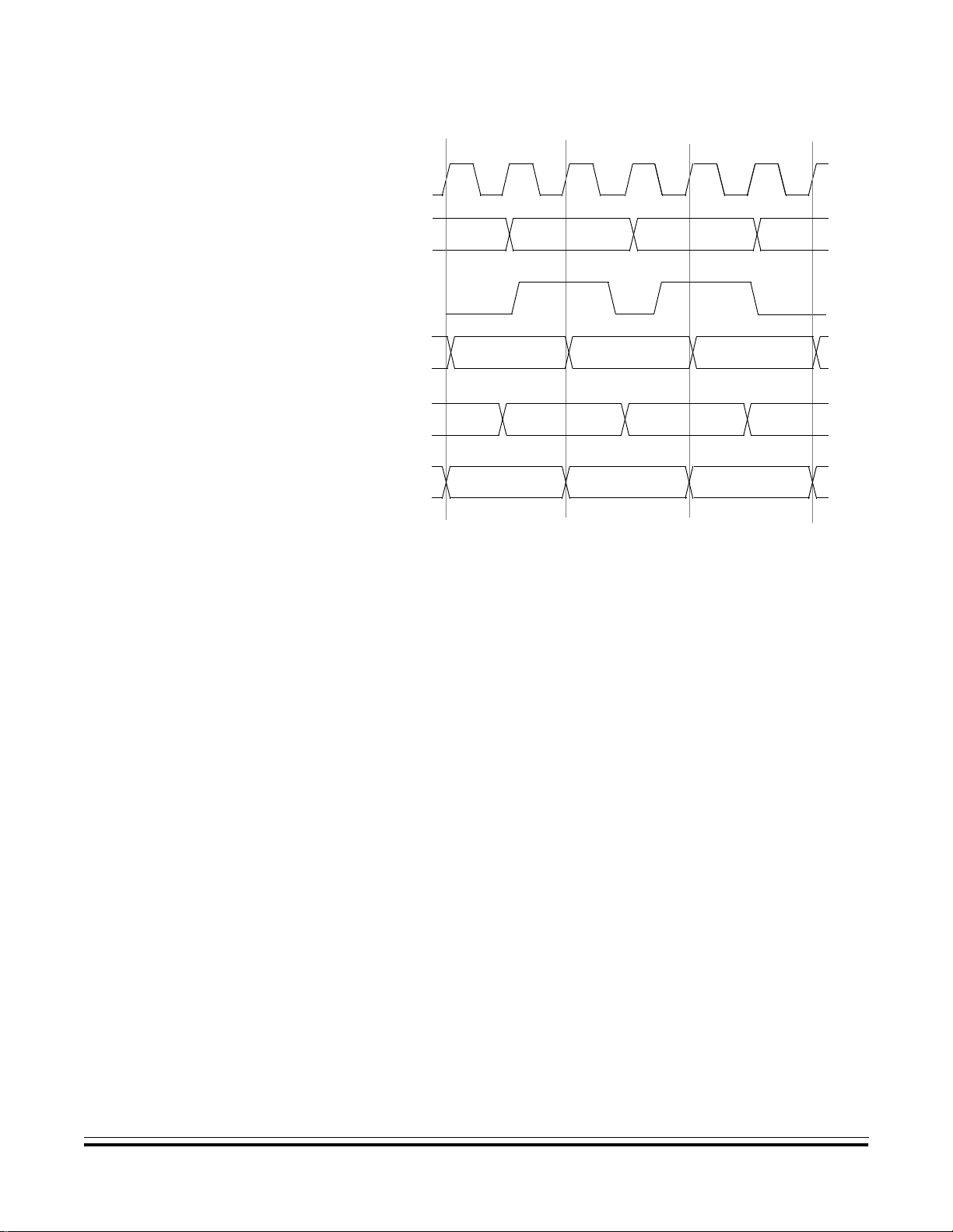
Figur e 2-10. Instru ction Boundaries
Reference Manual CPU08 — Rev. 3.0
34 Architecture MOTOROLA
Page 35

Architecture
CPU08 Functional Description
CPU CLOCK
OPCODE
LOOKAHEAD
REGISTER
LASTBOX
OPCODE LOOKAHEAD
IR/CONTROL
UNIT STATE
INPUT
CONTROL UNIT
STROBE
CONTROL UNIT
OUTPUT TO
EXECUTION UNIT
INTERNAL
ADDRESS BUS
OPCODE LOOKAHEAD/DECODE
LDA INSTRUCTION
T2 T3 T4 T1 T2 T3 T4
T1
TAX OPCODE
TAX
STATE 1
TAX EU CONTROL
LDA OP CODE
PREFETCH
$0103 $0104 $0105 $0052 $0106
LDA STATE 1 LDA STATE 2
LDA CY CLE
1 STROBE
LDA OFFSET FETCH INCX OPCODE PREFETCH LDA OPERAND READ
LDA OPCODE INCX OPCODE
LDA CYCLE 1
EU CONTROL
OPCODE LOOKAHEAD D ECO DE IN CX
INCX INSTRUCTION
T1 T2 T3 T4
LDA STATE 3
LDA CYCLE
2 STROBE
LDA CYCLE 2
EU CONTROL
INSTRUCTION
T1 T2 T3 T4
LDA CYCLE
3 STROBE
LDA CYCLE 3
EU CONTROL
STA OPCODE
INCX STATE 1
PREFETCH
INTERNAL
DATA BUS
INSTRUCTION
EXECUTION
BOUNDARIES
LDA OPCODE INCX OPCODE
$E6 $02 $5C $56
TAX LDA
Figure 2-11. Instruction Execution Timing Diagram
CPU08 — Rev. 3.0 Ref erence Manual
MOTOROLA Architecture 35
Page 36

Architecture
Reference Manual CPU08 — Rev. 3.0
36 Architecture MOTOROLA
Page 37

Reference Manual — CPU08
3.1 Contents
3.2 Introduction. . . . . . . . . . . . . . . . . . . . . . . . . . . . . . . . . . . . . . . .38
3.3 Elements of Reset and Interrupt Processing . . . . . . . . . . . . . .39
3.3.1 Recognition . . . . . . . . . . . . . . . . . . . . . . . . . . . . . . . . . . . . .39
3.3.2 Stacking . . . . . . . . . . . . . . . . . . . . . . . . . . . . . . . . . . . . . . . .40
3.3.3 Arbitration. . . . . . . . . . . . . . . . . . . . . . . . . . . . . . . . . . . . . . .41
3.3.4 Masking . . . . . . . . . . . . . . . . . . . . . . . . . . . . . . . . . . . . . . . .43
3.3.5 Returning to Calling Program. . . . . . . . . . . . . . . . . . . . . . . .45
3.4 Reset Processing . . . . . . . . . . . . . . . . . . . . . . . . . . . . . . . . . . .46
3.4.1 Initial Conditions Established . . . . . . . . . . . . . . . . . . . . . . . .47
3.4.2 CPU . . . . . . . . . . . . . . . . . . . . . . . . . . . . . . . . . . . . . . . . . . .47
3.4.3 Operating Mode Selection . . . . . . . . . . . . . . . . . . . . . . . . . .47
3.4.4 Reset Sources . . . . . . . . . . . . . . . . . . . . . . . . . . . . . . . . . . .48
3.4.5 External Reset . . . . . . . . . . . . . . . . . . . . . . . . . . . . . . . . . . .49
3.4.6 Active Reset from an Internal Source. . . . . . . . . . . . . . . . . .49
Section 3. Resets and Interrupts
3.5 Interrupt Processing . . . . . . . . . . . . . . . . . . . . . . . . . . . . . . . . .49
3.5.1 Interrupt Sources and Priority. . . . . . . . . . . . . . . . . . . . . . . .51
3.5.2 Interrupts in Stop and Wait Modes. . . . . . . . . . . . . . . . . . . .52
3.5.3 Nesting of Multiple Interrupts . . . . . . . . . . . . . . . . . . . . . . . .52
3.5.4 Allocating Scratch Space on the Stack . . . . . . . . . . . . . . . .53
CPU08 — Rev. 3.0 Reference Manual
MOTOROLA Resets and Interrupts 37
Page 38

Resets and Interrup ts
3.2 Introduction
The CPU08 in a microcontroller executes instructions sequentially. In
many applications it is necessary to execute sets of instructions in
response to requests from various peripheral devices. These requests
are often asynchronous to the execution of the main program. Resets
and interrupts are both types of CPU08 exceptions. Entry to the
appropriate service routine is called exception processing.
Reset is required to initialize the device into a known state, including
loading the prog ram counter (PC) with the address of the firs t instruction.
Reset and interrupt operations share the common concept of vector
fetching to force a new starting point for further CPU08 operations.
Interrupts provide a way to suspend normal program execution
temporarily so that the CPU08 can be freed to service these requests.
The CPU08 can pro c ess up t o 128 separ ate int erru pt sou rces incl u ding
a software interrupt (SWI).
On-chip peripheral systems generate maskable interrupts that are
recognized only if th e global interrupt mask bi t (I bit) in the condition co de
register is clear (reset is non-maskable). Maskable interrupts are
prioritized according to a default arrangement. (See Table 3-2 and
3.5.1 Interr upt Sou rces and Priori ty.) When inter rupt cond itions occur
in an on-chip perip heral system, an interrupt sta tus flag is set to indicate
the condition. When the user’s program has properly responded to this
interrupt request, the status flag must be cleared.
Reference Manual CPU08 — Rev. 3.0
38 Resets and Interrupts MOTOROLA
Page 39

3.3 Elements of Reset and Interrupt Processing
Reset and interru pt processing is handled in d iscrete, though some times
concurrent, tasks. It is comprised of interrupt recognition, arbitration
(evaluating interr upt priority), stacking of the mach ine state, and fetching
of the appropriate vector. Interrupt processing for a reset is comprised of
recognition and a fetch of the reset vector only. These tasks, together
with interrupt masking and returning from a service routine, are
discussed in this subsection.
3.3.1 Recognition
Reset recognition is asynchronous and is recognized when asserted.
Internal resets are asynchronous with instruction execution except for
illegal opcode and illegal address, which are inherently
instruction-synchronized. Exiting the reset state is always synchronous.
Resets and Interrupts
Elements of Reset and Interrupt Processing
All pending interrupts ar e recognized by the CPU08 durin g the last cycle
of each instruction. Interrupts that occur during the last cycle will not be
recognized by the CPU08 until the last cycle of the following instruction.
Instruction execution cannot be suspended to service an interrupt, and
so interrupt latency calculations must include the execution time of the
longest instruction that could be encountered.
When an interrupt is recognized, an SWI opcode is forced into the
instruction registe r in place of what would have been the next instructi on.
(When using th e C PU 08 with the direct mem ory access (DMA ) modu le,
the DMA can suspend instruction operation to service the peripheral.)
Because of the opcode “lookahead” pre fetch mech anism, at in structio n
boundaries th e program counter (P C) always points to t he address of the
next instruction to b e executed plus one. The pr esence of an in terrupt i s
used to modify the SW I flow such that instead of stacking this P C value,
the PC is decremented bef ore being stacked. Af ter interrupt servicing is
complete, the return-from-interrupt (RTI) instruction will unstack the
adjusted PC and use it to prefetch the next instruction again. After SWI
interrupt servicing is complete, the RTI instruction then fetches the
instruction following the SWI.
CPU08 — Rev. 3.0 Ref erence Manual
MOTOROLA Resets and Interrupts 39
Page 40

Resets and Interrup ts
3.3.2 Stacking
To maintain object code compatibility, the M68HC08 interrupt stack
frame is identical to that of the M6805 Family, as shown in Figure 3- 1.
Registers are stacked in the order of PC, X, A, and CCR. They are
unstacked in reverse order. Note that the condition code re gister (CCR)
I bit (internal mask) is not set until after the CCR is stacked du ring cycle 6
of the interrupt stacking procedure. The stack pointer always points to
the next available (empty) stack location.
UNSTACKING
ORDER
5
1
4
2
3
3
2
4
1
5
70
•
•
•
CONDITION CODE REGISTER
ACCUMULATOR
INDEX REGISTER (LOW BYTE X)
PROGRAM COUNTER HIGH
PROGRAM COUNTER LOW
(1)
•
•
STACKING
ORDER
1. High byte (H) of index register is not stacked.
•
$00FF (DEFAULT ADDRESS
ON RESET)
Figure 3-1. Interrupt Stack Frame
Reference Manual CPU08 — Rev. 3.0
40 Resets and Interrupts MOTOROLA
Page 41

Resets and Interrupts
Elements of Reset and Interrupt Processing
NOTE: To maintain compatibility with the M6805 Family, H (the high byte of the
index register) is not stacked dur ing interrupt pro cessing. If the inter rupt
service routine modifies H or uses the indexed addressing mode, it is
the user’s responsibility to save and restore it prior to returning.
See Figure 3-2.
IRQINT PSHH
|
|Inter ru pt se rv ic e ro ut ine
|
|
PULH
RTI
3.3.3 Arbitration
Figure 3-2. H Register Storage
All reset sources always have equal and highest priority and cannot be
arbitrated. Interrupts are latched, and arbitration is performed in the
system integration module ( SIM) at the start of interr upt processing. The
arbitration result is a constant that the CPU08 uses to determine which
vector to fetch. Once an interrupt is latched by the SIM, n o other interrupt
may take precedence, rega rdless of pr iority, unti l the latc hed interru pt is
serviced (or the I bit is cleared). See Figure 3 -3.
CPU08 — Rev. 3.0 Ref erence Manual
MOTOROLA Resets and Interrupts 41
Page 42

Resets and Interrup ts
BUS CYCLE #
1
2
3
4
5
6
INTERRUPT PROCESSING
7
8
1
LAST CYCLE OF
CURRENT INSTRUCTION
FETCH (REDUNDANT)
INTER RUPT HIGH BYTE
INTE RRUPT LOW BYTE
(A)
COMPLETE NE XT
INSTRUCTION (B)
STACK PCL
STACK PCH
STACK X
STACK A
STACK CCR
FETCH VECTOR
FETCH VECTOR
RTI
COMPLETE NEXT
INSTRUC TION
FETCH (REDUNDANT)
UNSTACK CCR
UNSTACK A
UNSTACK X
UNSTACK PCH
UNSTACK PCL
FETCH NEXT
INSTRUCTION (B)
INTERRUPT
PENDING?
NOTE 1
NO
YES
BUS CYCLE #
1
2
3
4
5
6
7
START INTERRUPT
PROCESSING
FETCH INTERRUPT
9
SERVICE ROUTINE
EXECUTE INTERRUPT
SERVICE ROUTINE
FIRST INSTRUCTION
FIRST CYCLE OF
NEXT INSTRUCT ION (B )
Note 1. Interrupts that occur before this point are recognized.
Figure 3-3. Interrupt Processing Flow and Timing
Reference Manual CPU08 — Rev. 3.0
42 Resets and Interrupts MOTOROLA
Page 43

3.3.4 Masking
Resets and Interrupts
Elements of Reset and Interrupt Processing
Reset is non-maskable. All other interrupts can be enabled or disabled
by the I mask bit in the CCR or by local mask bits in the periphera l control
registers. The I bit may also be mo dified by execution of the set inter rupt
mask bit (SEI) , clear i nte rrup t mask bit (CLI ), or tr ans fer accumu la tor to
condition code regi ster (TAP) instructions. The I bit is modified in the firs t
cycle of each instruction (these are all 2-cycle instructions). The I bit is
also set during interrupt processing (see 3.3.1 Recognition) and is
cleared during the second cycle of the RTI instruction when the CCR is
unstacked, provided that the stacked CCR I bit is not modified at the
interrupt service routine. (See 3.3.5 Returning to Calling Program.)
In all cases where the I bit can be modified, it is modified at least one
cycle prior to the last cycle of the instruction or operation, which
guarantees that the new I-bit state will be effective prior to execution of
the next instr uction. Fo r ex ample, if a n inte rrupt is recogni zed durin g the
CLI instruction, the load accumulator fro m memory (LDA) in struction will
not be executed before the interrupt is serviced. See Figure 3-4.
CLI
LDA #$FF
INT1 PSHH
|
|
|
PULH
RTI
INT1 Interrupt Service
Routine
Figure 3-4. Interrupt Recognition Example 1
Background
Routine
CPU08 — Rev. 3.0 Ref erence Manual
MOTOROLA Resets and Interrupts 43
Page 44

Resets and Interrup ts
If an interrupt is pending upon exit from the original interrupt service
routine, it will also be serviced before the LDA instruction is executed.
Note that the LDA op code is pr efetche d by both the INT 1 and INT 2 RTI
instructions. However, in the case of the INT1 RTI prefetch, this is a
redundant operation. See Figure 3-5.
CLI
LDA #$FF
INT1 PSHH
|
|
PULH
RTI
INT2 PSHH
|
|
PULH
RTI
INT1 Interrupt Service
Routine
INT2 Interrupt Service
Routine
Figure 3-5. Interrupt Recognition Example 2
Background
Routine
Similarly, in Figure 3-6, if an interrupt is recognized during the CLI
instruction, it will be serviced before the SEI instruction sets the I bit in
the CCR.
CLI
SEI
INT1 PSHH
|
|
PULH
RTI
INT1 Interrupt Service
Routine
Figure 3-6. Interrupt Recognition Example 3
Reference Manual CPU08 — Rev. 3.0
44 Resets and Interrupts MOTOROLA
Page 45

3.3.5 Returning to Calling Program
When an interrupt has been serviced, the RTI instruction terminates
interrupt processing and returns to the program that was running at the
time of the in terrupt. In servicing the inte rru pt, som e o r all of the CP U08
registers will have changed. To continue the former pr ogra m as though
uninterrupte d, the registers must be restored to the values present at the
time the former progra m was inter rupted. The RTI in struction take s care
of this by pulling (loading) the saved register values from the stack
memory. The last value to be pulled from the stack is the program
counter, which causes processing to resume at the point where it was
interrupted.
Unstacking the CCR generally clea rs the I bit, which is cleared du ring the
second cycle of the RTI instruction.
Resets and Interrupts
Elements of Reset and Interrupt Processing
NOTE: Since the return I bit state comes from the stacked CCR, the user, by
setting the I bit in the stacked CCR, can block all subsequent interrupts
pending or otherwise, regardless of priority, from within an interrupt
service routine.
LDA #$08
ORA 1,SP
STA 1,SP
RTI
This capability can be useful in handling a transient situation where the
interrupt handler detects that the background program is temporarily
unable to cope with the interrupt load and needs some time to recover.
At an appropriate juncture, the background program would reinstate
interrupts after it has recovered.
CPU08 — Rev. 3.0 Ref erence Manual
MOTOROLA Resets and Interrupts 45
Page 46

Resets and Interrup ts
3.4 Reset Processing
Reset forces the microcontroller unit (MCU) to assume a set of initial
conditions and to begin executing instructions from a predetermined
starting address. For the M68HC08 Family, reset assertion is
asynchronous with instruction execution, and so the initial conditions can
be assumed to take effect almost immediately after applying an active
low level to the reset pin, regardless of whether the clock has started.
Internally, reset is a clocked process, and so reset negation is
synchronous with an internal clock, as shown in Figure 3-7, which
shows the internal timing for exiting a pin reset.
CPU CLOCK
INTER NAL
ADDRESS BUS
INTER NAL
DATA BUS
RESET PIN
T3 T4 T1 T2 T3 T4 T1 T2 T3 T4 T1 T2 T3 T4 T1 T2 T3 T4 T1 T2 T3 T4
INDETERMINATE
INDETERMINATE
RESET PIN SAMPLING
$FFFF$FFFE
PCH
Figure 3-7. Exiting Reset
The reset system is able to actively pull down the reset output if
reset-causing conditions are detected by internal systems. This feature
can be used to reset external peripherals or other slave MCU devices.
Reference Manual CPU08 — Rev. 3.0
46 Resets and Interrupts MOTOROLA
Page 47

3.4.1 Initial Conditions Established
Once the reset condition is recognized, internal registers and contr ol bits
are forced to an initial state. These initial states are de scribed througho ut
this manual. These initial states in turn control on-chip peripheral
systems to force them to known startup states. Most of the initial
conditions are independent of the operating mode. This subsection
summarizes the initial conditions of the CPU08 and input/outpu t (I/O) as
they leave reset.
3.4.2 CPU
After reset the CPU08 fetches the re set vector from locati ons $FFFE and
$FFFF (when in monitor mode, the reset vector is fetched from $FEFE
and $FEFF), loads the vector into the PC, and begins executing
instructions. The stack pointer is loaded with $00FF. The H register is
cleared to provide compatibility for existing M6805 object code. All other
CPU08 registers ar e indeterminate immediately after reset; however, the
I interrupt mask bit in the condition code register is set to mask any
interrupts, and the STOP and WAIT latches are both cleared.
Resets and Interrupts
Reset Processing
3.4.3 Operating Mode Selection
The CPU08 has two modes of operation useful to the user:
• User mode
• Monitor mode
The monitor mode is the same as user mode except that alternate
vectors are used by forcing address bit A8 to 0 instead of 1. The reset
vector is therefo re fe tched from addr esses $F EFE and FEFF i nstead of
FFFE and FF FF. T his offset a llows the CP U08 to exe cute code from th e
internal monitor firmware instead of the user code. (Refer to the
appropriate tech nical data man ual for specific infor mation regar ding the
internal monitor description.)
CPU08 — Rev. 3.0 Ref erence Manual
MOTOROLA Resets and Interrupts 47
Page 48

Resets and Interrup ts
The mode of operation is latched on the rising edge of the reset pin. The
monitor mode is selected by connecting two port lines to Vss and
applying an over-voltage of approximately 2 x VDD to the IRQ1 pin
concurrent with the rising edge of reset (see Table 3-1). Port allocation
varies from port to port.
Table 3-1. Mode Selec tio n
IRQ1 Pin Port x Port y Mode
3.4.4 Reset Sources
≤ V
2 x V
DD
DD
XXUser
10Monitor
The system integr ation modu le (SIM ) ha s ma ster reset contr ol an d m ay
include, depending on devi ce implementa tion, any of the se typical r eset
sources:
• External reset (RESET pin)
• Power-on reset (P OR) circuit
• COP watchdog
• Illegal opcode reset
• Illegal address reset
• Low voltage inhibit (LVI) reset
A reset immediate ly stops exe cution of the c urrent i nstruction. All resets
produce the vector $FFFE/$FFFF and assert the internal reset signal.
The interna l reset causes all registers to return to their defaul t values and
all modules to return to their reset state.
Reference Manual CPU08 — Rev. 3.0
48 Resets and Interrupts MOTOROLA
Page 49

3.4.5 External Reset
A logic 0 applied to the RESET pin asserts the internal reset signal,
which halts all processing on the chip. The CPU08 and peripherals are
reset.
3.4.6 Active Reset from an Internal Source
All internal reset sources actively pull down the RESET pin to allow the
resetting of e xternal periphe ral s. Th e RES ET pin w ill be pulled do wn for
16 bus clock cycles; th e interna l reset signal will con tinue to b e asserted
for an additional 16 cycles after that. If the RESET
the end of the secon d 16 cycles, the n an exte rnal reset ha s occurr ed. If
the pin is high, the appropriate bit will be set to indicate the source of the
reset.
Resets and Interrupts
Interrupt Processing
pin is still low at the
The active reset feature allows the part to issue a reset to peripherals
and other chips within a system built around an M68HC08 MCU.
3.5 Interrupt Processing
The group of instructions executed in response to an interrupt is called
an interrupt service routine. These routines are much like subroutines
except that they are called through the automatic hardware interrupt
mechanism rather than by a subroutine call instruction, and all CPU08
registers, except the H register, are saved on the stack. Refer to the
description of the interrupt mask (I) found in 2.3.5 Cond itio n Code
Register.
An interrupt (provided it is enabled) causes normal program flow to be
suspended as soon as the currently executing instruction finishes. The
interrupt logic then pushes the contents of al l CPU08 reg isters onto the
stack, except the H register, so that the CPU08 content s can be restored
after the interrupt is finished. After stacking the CPU08 registers, the
vector for th e high est pr iori ty pendin g inter rup t sour ce is lo aded into th e
program counter an d executio n continues wit h the first instruction of the
interrupt service routine.
CPU08 — Rev. 3.0 Ref erence Manual
MOTOROLA Resets and Interrupts 49
Page 50

Resets and Interrup ts
An interrupt is concluded with a return-from-interrupt (RTI) instruction,
which causes all CPU08 registers and the return address to be
recovered from the stack, so th at the interrupted progra m can resume as
if there had been no interruption.
Interrupts can be enabled or disabled by the mask bit (I bit) in the
condition code register and by local enable mask bits in the on-chip
peripheral control registers. The interrupt mask bits in the CCR provide
a means of controlling the nesting of interrupts.
In rare cases it may be useful to allow an interrupt routine to be
interrupted (see 3.5.3 Nesting of Multiple Interrupts). However,
nesting is discouraged because it greatly complicates a system and
rarely improves system performance.
By default, the interrupt structure inhibits interrupts during the interrupt
entry sequence by setting the interrupt mask bit(s) in the CCR. As the
CCR is recovered from the stack during the return from interrupt, the
condition code bits return to the enabled state so that additional
interrupts can be serviced.
Upon reset, the I bit is set t o inhibit a ll interr upts. After minim um system
initialization, soft ware may clear the I bit by a T AP or CLI instruction, thus
enabling interrupts.
Reference Manual CPU08 — Rev. 3.0
50 Resets and Interrupts MOTOROLA
Page 51

3.5.1 Interrupt Sources and Priority
The CPU08 can have 128 separate vecto rs including re set and software
interrupt (SWI), which leaves 126 inputs for independent interrupt
sources. See Table 3-2.
NOTE: Not all CPU08 versions use all available interrupt vectors.
Address Reset Priority
FFFE Reset 1
FFFC SWI 2
FFFA IREQ[0] 3
:::
Resets and Interrupts
Interrupt Processing
Table 3-2. M68HC08 Vectors
FF02 IREQ[124] 127
FF00 IREQ[125] 128
When the system integration module (SIM) receives an interrupt
request, processing begins at the next instruction boundary. The SIM
performs the priority decoding necessary if more than one interrupt
source is active at the same time. Also, the SIM encodes the highest
priority interru pt request into a con stant that the CPU08 uses to g enerate
the corresponding interrupt vector.
NOTE: The interrupt source priority for any specific module may not always be
the same in different M68HC08 versions. For details about the priority
assigned to interr upt sources in a spe cific M68HC 08 device, r efer to the
SIM section of the technical data manual written for that device.
As an instructi on, SW I has the highest p riority othe r t han reset ; once the
SWI opcode is fetched, no other inter rupt can be hon ored until the SWI
vector has been fetched.
CPU08 — Rev. 3.0 Ref erence Manual
MOTOROLA Resets and Interrupts 51
Page 52

Resets and Interrup ts
3.5.2 Interrupts in Stop and Wait Modes
In wait mode the CPU clocks are disabled, but other module clocks
remain active. A module that is active during wait mode can wake the
CPU08 by an interrupt if the interrupt is enabled. Processing of the
interrupt begins immediately.
In stop mode, th e syste m clock s do not run. Th e syste m con trol modu le
inputs are conditioned so that they can be asynchronous. A particular
module can wake the part from stop mod e with an interrupt provided that
the module has been designed to do so.
3.5.3 Nesting of Multiple Interrupts
Under normal circumstances, CPU08 interrupt processing arbitrates
multiple pending interrupts, selects the highest, and leaves the rest
pending. The I bit in the CCR is also set, preventing nesting of interrupts.
While an interrupt is being serviced, it effectively becomes the highest
priority task for the system. When servicing is complete, the assigned
interrupt priority is re-established.
In certain systems wh ere, for example, a low priority inte rrupt contains a
long interrup t service routine, it may not be desirable to lock out all hi gher
priority interrupts while the low priority interrupt executes. Although not
generally advi sable, controll ed nesting of interrupts can be used to so lve
problems of this nature.
If nesting of interrupts is desired, the interrupt mask bit(s) must be
cleared after entering the interrupt service routine. Care must be taken
to specifically mask (disable) the present interrupt with a local enable
mask bit or clear the inte rrupt sour ce flag bef ore clearing the mask bit in
the CCR. Failure to do so will cause the same source to immediately
interrupt, which will rapidly consume all available stack space.
Reference Manual CPU08 — Rev. 3.0
52 Resets and Interrupts MOTOROLA
Page 53

3.5.4 Allocating Scratch Space on the Stack
In some systems, it is useful to allocate local variable or scratch space
on the stack for u se by the interr upt ser vi ce ro utine. T emp orar y stora ge
can also be obtained using the push (PSH) and pull (PUL) instructions;
however, the last-in-first-out (LIFO) structure of the stack makes this
impractical for more than one or two bytes. The CPU08 features the
16-bit add imm ediate val ue ( signed) to sta ck pointe r (A IS) i ns truction to
allocate space. T he stack pointer indexin g instructions ca n then be used
to access this data space, as demonstrated in this example.
IRQINT PSHH ;Save H register
AIS #-16 ;Allocate 16 bytes of local storage
STA 3,SP ;Store a value in the second byte
* Note: The stack pointer must always point to the next
* empty stack location. The location addressed
* by 0,SP should therefore never be used unless the
* programmer can guarantee no subroutine calls from
* within the interrupt service routine.
.
.
.
LDA 3,SP ;Read the value at a later time
.
.
.
AIS #16 ;Clean up stack
PULH ;Restore H register
RTI ;Return
Resets and Interrupts
Interrupt Processing
;of local space
* Note: Subroutine calls alter the offset from the SP to
* the local variable data space because of the
* stacked return address. If the user wishes to
* access this data space from subroutines called
* from within the interrupt service routine, then
* the offsets should be adjusted by +2 bytes for each
* level of subroutine nesting.
CPU08 — Rev. 3.0 Ref erence Manual
MOTOROLA Resets and Interrupts 53
Page 54

Resets and Interrup ts
Reference Manual CPU08 — Rev. 3.0
54 Resets and Interrupts MOTOROLA
Page 55

Reference Manual — CPU08
4.1 Contents
4.2 Introduction. . . . . . . . . . . . . . . . . . . . . . . . . . . . . . . . . . . . . . . .55
4.3 Addressing Modes . . . . . . . . . . . . . . . . . . . . . . . . . . . . . . . . . .56
4.3.1 Inherent . . . . . . . . . . . . . . . . . . . . . . . . . . . . . . . . . . . . . . . .57
4.3.2 Immediate. . . . . . . . . . . . . . . . . . . . . . . . . . . . . . . . . . . . . . .59
4.3.3 Direct . . . . . . . . . . . . . . . . . . . . . . . . . . . . . . . . . . . . . . . . . .61
4.3.4 Extended . . . . . . . . . . . . . . . . . . . . . . . . . . . . . . . . . . . . . . .63
4.3.5 Indexed, No Offset. . . . . . . . . . . . . . . . . . . . . . . . . . . . . . . .65
4.3.6 Indexed, 8-Bit Offset. . . . . . . . . . . . . . . . . . . . . . . . . . . . . . .65
4.3.7 Indexed, 16-Bit Offset. . . . . . . . . . . . . . . . . . . . . . . . . . . . . .66
4.3.8 Stack Pointer, 8-Bit Offset . . . . . . . . . . . . . . . . . . . . . . . . . .68
4.3.9 Stack Pointer, 16-Bit Offset . . . . . . . . . . . . . . . . . . . . . . . . .68
4.3.10 Relative . . . . . . . . . . . . . . . . . . . . . . . . . . . . . . . . . . . . . . . .71
4.3.11 Memory-to-Memory Immediate to Direct . . . . . . . . . . . . . . .73
4.3.12 Memory-to-Memory Direct to Direct. . . . . . . . . . . . . . . . . . .73
4.3.13 Memory-to-Memory Indexed to Direct
4.3.14 Memory-to-Memory Direct to Indexed
4.3.15 Indexed with Post Increment . . . . . . . . . . . . . . . . . . . . . . . .77
4.3.16 Indexed, 8-Bit Offset with Post Increment . . . . . . . . . . . . . .78
Addressing Modes
Contents
Section 4. Addressing Modes
with Post Increment. . . . . . . . . . . . . . . . . . . . . . . . . . . . .74
with Post Increment. . . . . . . . . . . . . . . . . . . . . . . . . . . . .76
4.4 Instruction Set Summary . . . . . . . . . . . . . . . . . . . . . . . . . . . . . 79
4.5 Opcode Map. . . . . . . . . . . . . . . . . . . . . . . . . . . . . . . . . . . . . . .87
4.2 Introduction
This section describes the addressing modes of the M68HC08 central
processor unit (CPU).
CPU08 — Rev. 3.0 Ref erence Manual
MOTOROLA Addressing Modes 55
Page 56

Addressing Modes
4.3 Addressing Modes
The CPU08 uses 16 addressing modes for flexibility in accessing data.
These addressi ng modes defi ne how the CPU finds the data req uired to
execute an instruction.
The 16 addressing modes are:
• Inherent
• Immediate
• Direct
• Extended
• Indexed, no offset
• Indexed, 8-bit offset
• Indexed, 16-bit offset
• Stack pointer, 8-bit offset
• Stack pointer, 16-bit offset
• Relative
• Memory-to-memory (four modes):
– Immediate to direct
– Direct to direct
– Indexed to direct with post increment
– Direct to indexed with post increment
• Indexed with post increment
• Indexed, 8-bit offset with post increment
Reference Manual CPU08 — Rev. 3.0
56 Addressing Modes MOTOROLA
Page 57

4.3.1 Inherent
Addressing Modes
Addressing Modes
Inherent instructions have no operand fetch associated with the
instruction, such as decima l adj u st accu mulato r ( DAA), cl ear i nde x high
(CLRH), and divi de (DIV ). Some o f the inher ent ins t ruction s act o n da ta
in the CPU registers, such as clear accumulator (CLRA), and transfer
condition code register to the accumulator (TPA). Inherent instructions
require no memory a ddress, and most are one byte lo ng. Tabl e 4- 1 lists
the instructions that use inherent addressing.
The assembly language statements shown here are examples of the
inherent addressing mode. In the code example and throughout this
section, bold typeface instructions are examples of the specific
addressing mode being discussed; a pound sign (#) before a number
indicates an immediate operand. The default base is decimal.
Hexadecimal numb ers are represented by a dollar sign ($) preceding the
number. Some assemblers use hexadecimal as the default numbering
system. Refer to the documentation for the particular assembler to
determine the proper syntax.
Machine
Code
A657 EX_1 LDA #$57 ;A = $57
AB45 ADD #$45 ;A = $9C
72 DAA ;A = $02 w/carry
A614 EX_2 LDA #20 ;LS dividend in A
8C CLRH ;Clear MS dividend
AE03 LDX #3 ;Divisor in X
52 DIV ;(H:A)/X→A=06,H=02
A630 EX_3 LDA #$30 ;A = $30
87 PSHA ;Push $30 on stack and
Label Operation Operand Comments
;bit set ≡ $102
;decrement stack
;pointer by 1
CPU08 — Rev. 3.0 Ref erence Manual
MOTOROLA Addressing Modes 57
Page 58

Addressing Modes
Table 4-1. Inherent Addressing Instructions
Instruction Mnemonic
Arithmetic Shift Lef t ASLA, ASLX
Arithmetic Shift Right ASRA, ASRX
Clear Carry Bit CLC
Clear Interrupt Mask CLI
Clear CLRA, CLRX
Clear H (Index Register High) CLRH
Complement COMA, COMX
Decimal Adjust Accumulator DAA
Decrement Accumulator, Branch if Not Equal ($00) DBNZA
Decrement X (Index Register Low), Branch if Not Equal ($00) DBNZX
Decrement DECA, DECX
Divide (Integer 16-Bit by 8-Bit Divide) DIV
Increment INCA, INCX
Logical Shift Left LSLA, LSLX
Logical Shift Right LSRA, LSRX
Multiply MUL
Negate NEGA, NEGX
Nibble Swap Accumulator NSA
No Operation NOP
Push Accumula to r o nt o Stack PSHA
Push H (Index Register High) onto Stack PSHH
Push X (Index Register Low) onto Stack PSHX
Pull Accum u lator from St ac k PULA
Pull H (Index Register High) from Stack PULH
Pull X (Index Register Low) from Stack PULX
Rotate Left through Carry ROLA, ROLX
Rotate Right through Carry RORA, RORX
Reset Stack Pointer to $00FF RSP
Return from Interrupt R TI
Return from Subroutine RTS
Set Carry Bit SEC
Set In te r rupt Ma sk SE I
Reference Manual CPU08 — Rev. 3.0
58 Addressing Modes MOTOROLA
Page 59

Addressing Modes
Addressing Modes
Table 4-1. Inherent Addressing Instructions (Continued)
Instruction Mnemonic
Enable IRQ and Stop Oscillator STOP
Software In t e rrupt SWI
Transfer Accumulator to Condition Code Register TAP
Transfer Accumulator to X (Index Register Low) TAX
Transfer Condition Code Register to Accumulator TPA
Test for Negative or Zero TSTA, TSTX
Transfer Stack Pointer to Index Register (H:X) TSX
Transfer X (Index Register Low) to Accumulator TXA
Transfer Index Register (H:X) to Stack Pointer TXS
Enable Interrupts and Halt CPU WAIT
4.3.2 Immediate
The operand in immediate instructions is contained in the bytes
immediately following the opcode. The byte or bytes that follow the
opcode are the value of the statement rather than the address of the
value. In this case, the effe ctive address of the instructi on is specified by
the # sign and implicitly points to the byte following the opcode. The
immediate value is limited to either one or two bytes, depending on the
size of the register involved in the instruction. Table 4-2 lists the
instructions that use immediate addressing.
Immediate instructions associated with the index register (H:X) are
3-byte instructio ns: one byte for the opcode, two bytes for the immedi ate
data byte.
The example code shown he re contains two immediate in structions: AIX
(add immed iate to H:X) and CPHX (co mpare H:X with immediate val ue).
H:X is first cl eared and th en increme nted by one until i t contain s $FFFF.
Once the condition specified by the CPHX becomes true, the program
branches to START, and the process is repeated indefinitely.
CPU08 — Rev. 3.0 Ref erence Manual
MOTOROLA Addressing Modes 59
Page 60

Addressing Modes
Machine
Code
5F START CLRX ;X = 0
8C CLRH ;H = 0
AF01 TAG AIX #1 ;(H:X) = (H:X) + 1
65FFFF CPHX #$FFFF ;Compare (H:X) to
26F9 BNE TAG ;Loop until equal
20F5 BRA START ;Start over
Label Operation Operand Comments
;$FFFF
Table 4-2. Immediate Addressing Instructions
Instruction Mnemonic
Add with Carry Immediate Value to Accumulator ADC
Add Immediate Value to Accumulator ADD
Add Immediate Value (Signed) to Stack Pointer AIS
Add Immediate Value (Signed) to Index Register (H:X) AIX
Logical AND Immediate Value with Accumulator AND
Bit Test Immediate Value with Accumulator BIT
Compare A with Immediate and Branch if Equal CBEQA
Compare X (Index Register Low) with Immediate and Branch if Equal CBEQX
Compare Accumulator with Immediate Value CMP
Compare Index Register (H:X) with Immediate Value CPHX
Compare X (Index Register Low) with Immediate Value CPX
Exc lusi ve OR Im medi ate Value with Acc umulato r EOR
Load Accumulator from Immediate Value LDA
Load Index Register (H:X) with Immediate Value LDHX
Load X (Index Register Low) from Immediate Value LDX
Inclusive OR Immediate Val ue ORA
Subtract with Carry Immediate Value SBC
Subtract Immediate Value SUB
Reference Manual CPU08 — Rev. 3.0
60 Addressing Modes MOTOROLA
Page 61

4.3.3 Direct
Addressing Modes
Addressing Modes
Most direct instructions can access any of the first 256 memory
addresses with only two bytes. The first byte is the opcode, and the
second is the low byte of the operand address. The high-order byte of
the effective address is assumed to be $00 and is not included as an
instruction byte (saving program memory space and execution time).
The use of d irect addr essing mode is therefore li mited to o perands in the
$0000–$00FF area of memory (called the direct page or page 0).
Direct addressing instructions take one less byte of program memory
space than the equivalent instructions using extended addressing. By
eliminating the additional memo ry access, the executi on time is redu ced
by one cycle. In the course of a long program, this savings can be
substantial. Most microcontroller units place some if not all
random-access memory (RAM) in the $0000–$00FF area; this allows
the designer to assign these locations to frequently referenced data
variables, thus saving execution time.
BRSET and BRCLR ar e 3-byte instructi ons that use dir ect addressing to
access the operand and relative addressing to specify a branch
destination.
CPHX, STHX, and LDHX are 2-byte instructions that fetch a 16-bit
operand. The most significant byte comes from the direct address; the
least significant byte comes from the direct address + 1.
Table 4-3 lists the instructions that use direct addressing.
This example code contains two direct addressing mode instructions:
STHX (store H:X in memory) and CPHX (compare H:X with memory).
The first STHX instruction initializes RAM storage location TEMP to
zero, and the second STHX instruction loads TEMP with $5555. The
CPHX instruction compares the value in H:X with the value of
RAM:(RAM + 1).
CPU08 — Rev. 3.0 Reference Manual
MOTOROLA Addressing Modes 61
Page 62

Addressing Modes
In this example, RAM:(RAM + 1) = TEMP = $50:$51 = $5555.
Machine
Code
5F START CLRX ;X = 0
8C CLRH ;H = 0
3550 STHX TEMP ;H:X=0 > temp
455555 LDHX #$5555 ;Load H:X with $5555
3550 STHX TEMP ;Temp=$5555
7550 BAD_PART CPHX RAM ;RAM=temp
26FC BNE BAD_PART ;RAM=temp will be
20F1 BRA START ;Do it again
Label Operation Operand Comments
RAM EQU $50 ;RAM equate
ROM EQU $6E00 ;ROM equate
ORG $RAM ;Beginning of RAM
TEMP RMB 2 ;Reserve 2 bytes
ORG $ROM ;Beginning of ROM
;same unless somet hing
;is very w rong!
Table 4-3. Direct Addressing Instructions
Instruction Mnemonic
Add Memory and Carry to Accumulator ADC
Add Memory and Accumulator ADD
Logical AND of Memory and Accumulator AND
Arithmetic Shift Left Memory
Arithmetic Shift Right Memory ASR
Clear Bit in Memory BCLR
Bit Test Memory with Accumulator BIT
Branch if Bit n in Memory Clear BRCLR
Branch if Bit n i n Me mory Set BRSET
Set Bit in Memory BSET
Compare Direct with Accumulator and Branch if Equal CBEQ
Clear Memory CLR
Compare Accumulator with Memory CMP
Complement Memory COM
Compare Index Register (H:X) with Memory CPHX
ASL
(1)
Reference Manual CPU08 — Rev. 3.0
62 Addressing Modes MOTOROLA
Page 63

Addressing Modes
Addressing Modes
Table 4-3. Direct Addressing Instructions (Continued)
Instruction Mnemonic
Compare X (Index Register Low) with Memory CPX
Decrement Memory and Branch if Not Equal ($00) DBNZ
Decrement Memory DEC
Exclusive OR Memory with Ac c u mulator EOR
Increment Memory INC
Jump JMP
Jum p to Subrou tine JSR
Load Accumulator from Memory LDA
Load Index Register (H:X) from Memory LDHX
Load X (Index Register Low) from Memory LDX
Logical Shift Left Memory
LSL
(1)
4.3.4 Extended
Logical Shift Right Memory LSR
Negate Memory NEG
Inclusive OR Accumulator and Memory ORA
Rotate Memory Left through Carry ROL
Rotate Memory Right through Carry ROR
Subtract Memory and Carry from Accumulator SBC
Store Accumulator in Memo ry STA
Store Index Register (H:X) in Memory STHX
Store X (Index Register Low) in Memory ST X
Subtr a c t Memory from Accumulator SUB
Test Memory for Negative or Zero TST
1. ASL = LSL
Extended instructions can access any address in a 64-Kbyte memory
map. All extende d instru ctions ar e thr ee bytes lo ng. Th e fi rst b yte is the
opcode; the second and third bytes are the most significant and least
significant bytes of the operand address. This addressing mode is
selected when m emory a bove the d irect or zero page ($ 0000–$00F F) is
accessed.
CPU08 — Rev. 3.0 Reference Manual
MOTOROLA Addressing Modes 63
Page 64

Addressing Modes
When using most a ssemblers, the pro grammer does n ot need to specify
whether an instruction is direct or extended. The assembler
automatically selects the short est fo rm of th e instruction. Ta ble 4-4 lists
the instructions that use the e xtended addressing mode. An exam ple o f
the extended addressing mode is shown here.
Machine
Code
5F CLRX
BE50 LDX $0050 ;Load X direct
5F CLRX
CE6E00 LDX $6E00 ;Load X extended
Label Operation Operand Comments
ORG $50 ;Start at $50
FCB $FF ;$50 = $FF
ORG $6E00 ;Start at $6E00
FCB $FF ;$6E00 = $FF
Table 4-4. Extended Addressing Instructions
Instruction Mnemonic
Add Memory and Carry to Accumulator ADC
Add Memory and Accumulator ADD
Logical AND of Memory and Accumulator AND
Bit Test Memory with Accumulator BIT
Compare Accumulator with Memory CMP
Compare X (Index Register Low) with Memory CPX
Exclusive OR Memory with Ac c u mulator EOR
Jump JMP
Jum p to Subrou tine JSR
Load Accumulator from Memory LDA
Load X (Index Register Low) from Memory LDX
Inclus ive OR Accumulato r w ith Memory OR A
Subtract Memory and Carry from Accumulator SBC
Store Accumulator in Memo ry STA
Store X (Index Register Low) in Memory STX
Subtr a c t Memory from Accumulator SUB
Reference Manual CPU08 — Rev. 3.0
64 Addressing Modes MOTOROLA
Page 65

4.3.5 Indexed, No Offset
Indexed instructions with no offset are 1-byte instructions that access
data with variable addresses. X contains the low byte of the conditional
address of the operand; H contains the high byte. Due to the addition of
the H register, this addressing mode is not limited to the first 256 bytes
of memory as in the M68HC05.
If none of the M68HC08 instructions that modify H are used
(AIX; CBEQ (ix+); LDHX; MOV (dir/ix+); MOV (ix+/dir); DIV; PULH;
TSX), then the H value will be $00, which ensures complete source code
compatibility with M68HC05 Family instructions.
Indexed, no offset instructions can move a pointer thro ugh a table or hold
the address of a frequently used RAM or input/output (I/O) location.
Table 4-5 lists instructions that use indexed, no offset addressing.
Addressing Modes
Addressing Modes
4.3.6 Indexed, 8-Bit Offset
Indexed, 8-b it offset instru cti ons are 2- byte i n structio ns tha t can a ccess
data with variabl e ad dresse s. The CPU ad ds the u nsigned bytes in H :X
to the unsigned byte following the opcode. The sum is the effective
address of the operand.
If none of the M68HC08 instructions that modify H are used
(AIX; CBEQ (ix+); LDHX; MOV (dir/ix+); MOV (ix+/dir); DIV; PULH;
TSX), then the H value will be $00, which ensures complete source code
compatibility with the M68HC05 Family instructions.
Indexed, 8-bit offset instructions are useful in selecting the kth element
in an n-elemen t table. The t able can begin anywhere and can exten d as
far as the address ma p allows. The k value would typically be i n H:X, and
the address of the beginning of the table would be in the byte following
the opcode . Using H:X in th is way, this ad dressing mode i s limited to the
first 256 addresses in memory. Tables can be located anywhere in the
address map when H:X is used as the base address, and the byte
following is the offset.
Table 4-5 lists the instructions that use indexed, 8-bit offset addre ssi ng.
CPU08 — Rev. 3. 0 Reference Manual
MOTOROLA Addressing Modes 65
Page 66

Addressing Modes
4.3.7 Indexed, 16-Bit Offset
Indexed, 16-b it offset instructions are 3-byte in structions that can access
data with variabl e ad dresse s at any lo cation i n memo ry. T he C PU adds
the unsigned contents of H:X to the 16-bit unsigned w ord formed by the
two bytes following the opcode. The sum is the effective address of the
operand. Th e first byte after the opcode is the most significant byte of the
16-bit offset; the second byte is the least significant byte of the offset.
As with direct and extended addressing, most assemblers determine the
shortest form of indexed ad dres sing. Tabl e 4-5 lists the instructions that
use indexed, 16-bit offset addressing.
Indexed, 16- bit offset in structions are useful in selecti ng the kth elemen t
in an n-elemen t table. The t able can begin anywhere and can exten d as
far as the address ma p allows. The k value would typically be i n H:X, and
the address of the beginn ing of the table wou ld be in the bytes following
the opcode.
This example uses th e JMP (uncondit ional jump) instr uction to show the
three different types of indexed addressing.
Machine
Code
FC JMP ,X ;No offset
ECFF JMP $FF,X ;8-bit offset
DC10FF JMP $10FF,X ;16-bit offset
Label Operation Operand Comments
;Jump to address
;pointed to by H:X
;Jump to address
;
pointed to by H:X + $FF
;Jump to address
;
pointed to by H:X + $10FF
Reference Manual CPU08 — Rev. 3.0
66 Addressing Modes MOTOROLA
Page 67

Addressing Modes
Addressing Modes
Table 4-5. Indexed Addressing Instructions
Instruction Mnemonic
No
Offset
8-Bit
Offset
16-Bit
Offset
Add Memory and Carry to Accumulator ADC ✔✔✔
Add Memory and Accumulator ADD ✔✔✔
Logical AND of Memory and Accumulator AND ✔✔✔
Arithmetic Shift Left Memory
ASL
(1)
✔✔—
Arithmetic Shift Right Memory ASR ✔✔—
Bit Test Memory with Accumulator BIT ✔✔✔
Clear Me mo ry CLR ✔✔—
Compare Accumulator with Memory CMP ✔✔✔
Compl e ment Memory COM ✔✔—
Compare X (Index Register Low)
with Memory
Decrement Memory and Branch if Not Equal
($00)
CPX ✔✔✔
DBNZ ✔✔—
Decrement Memory DEC ✔✔—
Exclusive OR Me mory with Accumulator EOR ✔✔✔
Increment Memory INC ✔✔—
Jump JMP ✔✔✔
Jump to Subroutine JSR ✔✔✔
Load Accumulator from Memory LDA ✔✔✔
Load X (Index Register Low) from Memory LDX ✔✔✔
Logical Shift Left Memory
LSL
(1)
✔✔—
Logical Shift Right Memory LSR ✔✔—
Negate Me mo ry NEG ✔✔—
Inclusive OR Accumulator and Memory ORA ✔✔✔
Rotate Memory Left through Carry ROL ✔✔—
Rotate Memory Right through Carry ROR ✔✔—
Subtract Memory and Carry from Accumulator SBC ✔✔✔
Store Accu mu lator in Memory STA ✔✔✔
Store X (Index Register Low) in Memory STX ✔✔✔
Subtract Memory from Accumulator SUB ✔✔✔
Test Memory for Negative or Zero TST ✔✔—
1. ASL = LSL
CPU08 — Rev. 3.0 Reference Manual
MOTOROLA Addressing Modes 67
Page 68

Addressing Modes
4.3.8 Stack Pointer, 8-Bit Offset
Stack pointer, 8-bit offset instructions are 3-byte instructions that
address operands in much the same way as indexed 8-bit offset
instructions, only the y add the 8-bit offset to the value of the stack point er
instead of the index register.
The stack pointer, 8-bit offset addressing mode permits easy access of
data on the stack. The CPU adds the unsigned byte in the 16-bit stack
pointer (SP) registe r to the unsigned byte following the opcod e. The sum
is the effective address of the operand.
If interrupts a re disa bled, th is addressi ng m ode a llows the sta ck pointe r
to be used as a second “index” register. Table 4-6 lists the instructions
that can be used in the stack pointer, 8-bit offset addressing mode.
Stack pointer relative instructions require a pre-byte for access.
Consequently, all SP relative instructions take one cycle longer than
their index relative counterparts.
4.3.9 Stack Pointer, 16-Bit Offset
Stack pointer, 16-bit offset instructions are 4-byte instructions used to
access data relative to the stack pointer with variable addresses at any
location in memory. The CPU adds the unsigned contents of the 16-bit
stack pointer register to the 16-bit unsigned word formed by the two
bytes following the opcode. The sum is the effective address of the
operand.
As with direct and extended addressing, most assemblers determine the
shortest form of stack pointer addressing. Due to the pre-byte, stack
pointer relative instructions take one cycle longer than their index
relative counterparts. Table 4-6 lists the instructions that can be used in
the stack pointer, 16-bit offset addressing mode.
Reference Manual CPU08 — Rev. 3.0
68 Addressing Modes MOTOROLA
Page 69

Addressing Modes
Addressing Modes
Examples of the 8-bit and 16-bit offset stack pointer addressing modes
are shown here. The first example stores the value of $20 in location
$10, SP = $10 + $FF = $10F and then decrements that location until
equal to zero. The second example loads the accumulator with the
contents of memory location $250, SP = $250 + $FF = $34F.
Machine
Code
450100 LDHX #$0100
94 TXS ;Reset stack pointer
A620 LDA #$20 ;A = $20
9EE710 STA $10,SP ;Location $10F = $20
9E6B10FC LP DBNZ $10,SP,LP ;8-bit offset
450100 LDHX #$0100
94 TXS ;Reset stack pointer
9ED60250 LDA $0250,SP ;16-bit offset
Label Operation Operand Comments
;to $00FF
;decrement the
;contents of $10F
;until equal to zero
;to $00FF
;Load A with contents
;of $34F
Stack pointer, 16-bit offset instructions are useful in selecting the kth
element in an n-element table. The table can begin anywhere and can
extend anywhere in memory. With this 4-byte instruction, the k value
would typically be in the stack pointer register, and the address of the
beginning of the table is located in the two bytes following the 2-byte
opcode.
CPU08 — Rev. 3.0 Reference Manual
MOTOROLA Addressing Modes 69
Page 70

Addressing Modes
Table 4-6. Stack Pointer Addressing Instructions
Instruction M nemonic
Add Memory and Carry to Accumulator ADC ✔✔
Add Memory and Accumulator ADD ✔✔
Logical AND of Memory and Accumulator AND ✔✔
Arithmetic Shift Left Memory
Arithmetic Shift Right Memory ASR ✔ —
Bit Test Memory with Accumulator BIT ✔✔
Compare Direct with Accumulator and
Branch if Equal
Clear Memory CLR ✔ —
Compare Accumulator with Memory CMP ✔✔
Complement Memory COM ✔ —
Compare X (Index Register Low) with Memory CPX ✔✔
Decrement Memory and Branch if
Not Equal ($00)
Decrement Memory DEC ✔ —
(1)
ASL
CBEQ ✔ —
DBNZ ✔ —
8-Bit
Offset
✔ —
16-Bit
Offset
Exclusive OR Memory with Ac c u mulator EOR ✔✔
Increment Memory INC ✔ —
Load Accumulator from Memory LDA ✔✔
Load X (Index Register Low) from Memory LDX ✔✔
Logical Shift Left Memory
Logical Shift Right Memory LSR ✔ —
Negate Memory NEG ✔ —
Inclusive OR Accumulator and Memory ORA ✔✔
Rotate Memory Left through Carry ROL ✔ —
Rotate Memory Right through Carry ROR ✔ —
Subtract Memory and Carry from Memory SBC ✔✔
Store Accumulator in Memo ry STA ✔✔
Store X (Index Register Low) in Memory STX ✔✔
Subtr a c t Memory from Accumulator SUB ✔✔
Test Memory for Negative or Zero TST ✔ —
1. ASL = LSL
LSL
(1)
✔ —
Reference Manual CPU08 — Rev. 3.0
70 Addressing Modes MOTOROLA
Page 71

4.3.10 Relative
Addressing Modes
Addressing Modes
All conditional branch instructions use relative addressing to evaluate
the resultant effective address (EA). T he CPU evaluates the conditional
branch destina tion by adding th e signed b yte following th e opcode to th e
contents of the program counter. If the branch condition is true, the PC
is loaded with the EA. If the branch condition is not true, the CPU goes
to the next instruction. The offse t is a signed, two’s comple ment byte that
gives a branching range of –128 to +127 bytes from the address of the
next location after the branch instruction.
Four new branch opcodes test the N, Z, and V (overflow) bits to
determine the relative signed values of the operands. These new
opcodes are BLT, B GT, BLE, and BGE and are desig ned to be used with
signed arithmetic operations.
When using most assemblers, the programmer does not need to
calculate the offset, b ecause the assembler deter mines the proper offset
and verifies that it is within the span of the branch.
Table 4-7 lists the instructions that use relative addressing.
This example contains two relative addressing mode instructions: BLT
(branch if less than, signed operation) and BRA (b ranch always).
In this example, the valu e i n th e accum ulator is com pare d to the sign ed
value –2. Because #1 is greater than –2 , the branch to TAG will not
occur.
Machine
Code
A601 TAG LDA #1 ;A = 1
A1FE
91FA
20FE HERE BRA HERE ;Branch always
Label Operation Operand Comments
CMP
BLT
#-2
TAG
;Compare with -2
;Branch if value of A
;is less th an -2
CPU08 — Rev. 3.0 Reference Manual
MOTOROLA Addressing Modes 71
Page 72

Addressing Modes
Table 4-7. Relative Addressing Instructions
Instruction Mnemonic
Branch if Carry Clear BCC
Branch if Carry Set BCS
Branch if Equal BEQ
Branch if Greater Than or Equal (Signed) BGE
Branch if Greater Than (Signed) BGT
Branch if Half-Carry Clear BHCC
Branch if Half-Carry Set BHCS
Branch if Higher BHI
Branch if Higher or Same BHS (BCC)
Branch if Interrupt Line High BIH
Branch if Interrupt Line Low BIL
Branch if Less Than or Equal (Signed) BLE
Branch if Lower BLO (BCS)
Branch if Lower or Same BLS
Branch if Less Than (Signed) BLT
Branch if Interrupt Mask Clear BMC
Branch if Minus BMI
Branch if Interrup t Mask Se t BMS
Branch if Not Equal BNE
Branch if Plus BPL
Branch Alway s BRA
Branch if Bit n in Memory Clear BRCLR
Branch if Bit n in Memory Set BRSET
Branch Never BRN
Branch to Subroutine BSR
Reference Manual CPU08 — Rev. 3.0
72 Addressing Modes MOTOROLA
Page 73

4.3.11 Memory-to-Memory Immediate to Direct
Move immediate to direct (MOV imm /dir) is a 3-byt e, 4-cycle ad dressing
mode generally used to initialize variables and registers in the direct
page. The operand in the byte immediately following the opcode is
stored in the direct page locatio n addressed by the se cond byte following
the opcode. The MOV instruction associate d with this addressi ng mode
does not affect the accumulator value. This example shows that by
eliminating th e accum ulator from the data tran sfer pr ocess, th e numb er
of execution cycles decreases from 9 to 4 for a similar im mediate to
direct operation.
Addressing Modes
Addressing Modes
Machine
Code
* Data movement with accumulator
B750 (2 cycles) PSHA ;Save current A
A622 (2 cycles) LDA #$22 ;A = $22
B7F0 (3 cycles) STA $F0 ;Store $22 into $F0
B650 (2 cycles) PULA ;Restore A value
9 cycles
* Data movement without accumulator
6E22F0
(4 cycles)
4.3.12 Memory-to-Memory Direct to Direct
Move direct to direct (MOV dir/dir) is a 3-byte, 5-cycle addr essing mode
generally used i n register-to -register mo vements of data fr om within the
direct page. The operand in the direct page location addressed by the
byte immediately following the opcode is stored in the direct page
location addressed by the second byte following the opcode. The MOV
instruction associated with this addressing mode does not affect the
accumulator value. As with the previous addressing mode,
Label Operation Operand Comments
; value
MOV #$22,$F0 ;Location $F0
;= $22
CPU08 — Rev. 3.0 Reference Manual
MOTOROLA Addressing Modes 73
Page 74

Addressing Modes
eliminating the accumulator from the data transfer process reduces the
number of execution cycles from 10 to 5 for similar direct-to-direct
operations (see exam ple). This savings can be substantial for a prog ram
containing numerous register-to-register data transfers.
Machine
Code
* Data movement with accumulator
B750 (2 cycles) PSHA ;Save A value
B6F0 (3 cycles) LDA $F0 ;Get contents
B7F1 (3 cycles) STA $F1 ;Location $F1=$F0
B650 (2 cycles) PULA ;Restore A value
10 cycles
* Data movement without accumulator
4EF0F1 ( 5 cycles) MOV $F0,$F1 ;Move contents of
Label Operation Operand Comments
4.3.13 Memory-to-Memory Indexed to Direct with Post Increment
Move indexed to dire ct, post increment (MOV ix+/dir) is a 2-byte, 4-cycle
addressing mode generally used to transfer tables addressed by the
index register to a re gi ster in the d irect p age. T he ta bles can be located
anywhere in the 64-Kbyte map and can be any size. This instruction
does not affect the accumulator value. The operand addressed by H:X
is stored in the direct page l ocat ion addr essed by the byt e foll owing the
opcode. H:X is incremented after the move.
;of $F0
;$F0 to $F1
This addressing mode is effective for transferring a buffer stored in RAM
to a serial transmit register, as shown in the following example. Table 4-8
lists the memory-to-memory move instructions.
NOTE: Move indexed to direct, po st increment instr uctions will increment H if X
is incremented past $FF.
Reference Manual CPU08 — Rev. 3.0
74 Addressing Modes MOTOROLA
Page 75

Addressing Modes
Addressing Modes
This example illustrates an interrupt-driven SCI transmit service routine
supporting a circular buffer.
Machine
Code
55 50 TX_INT LDHX PTR_OUT ;Load pointer
B6 16 LDA SCSR1 ;Dummy read of
7E 18 MOV X+, SCDR ;Move new byte to
65 00 64 CPHX #TX_B +
23 03 BLS NOLOOP ;If not, continue
45 00 54 LDHX #TX_B ;Else reset to
35 50 NOLOOP STHX PTR_OUT ;Save new
80 RTI ;Return
Label Operation Operand Comments
SIZE EQU 16 ;TX circular
;buffer length
SCSR1 EQU $16 ;SCI status
;register 1
SCDR EQU $18 ;SCI transmit
;data register
ORG $50
PTR_OUT RMB 2 ;Circular buffer
;data out pointer
PTR_IN RMB 2 ;Circular buffer
;data in pointer
TX_B RMB SIZE ;Circular buffer
*
* SCI transmit data register empty interrupt
* service routine
*
ORG $6E00
;SCSR1 as part of
;the TDRE reset
;SCI data reg.
;Clear TD R E . P o s t
;increment H:X.
;Gone past end of
SIZE
;circular buffer?
;start of buffer
;pointer value
CPU08 — Rev. 3.0 Reference Manual
MOTOROLA Addressing Modes 75
Page 76

Addressing Modes
4.3.14 Memory-to-Memory Direct to Indexed with Post Increment
Move direct to indexe d, post increment (MOV dir/ix+) is a 2-b yte, 4-cycle
addressing mode gene rally used to fill tables fro m registers in the direct
page. The tables can be locate d anywhere in the 64-Kbyte map and can
be any size. The instruction associated with this addressing mod e does
not affect the accumulator valu e. The operand in the direct page location
addressed by the byte imm ediately follo wing the opcode is stored in the
location addressed by H:X. H:X is incremented after the move.
An example of this addressing mode would be in filling a serial receive
buffer located in R AM fr om the recei ve data r egister . Table 4- 8 lists the
memory-to-memory move instructions.
NOTE: Move direct to indexed, post incr ement instructions will incr ement H if X
is incremented past $FF.
This example illustrates an interrupt-driven SCI receive service routine
supporting a circular buffer.
Machine
Code
Label Operation Operand Comments
SIZE EQU 16 ;RX circular
;buffer length
SCSR1 EQU $16 ;SCI status reg.1
SCDR EQU $18 ;SCI receive
;data reg.
ORG $70
PTR_OUT RMB 2 ;Circular buffer
;data out pointer
PTR_IN RMB 2 ;Circular buffer
;data in pointer
RX_B RMB SIZE ;Circular buffer
*
* SCI receive data register full interrupt
* service routine
*
Reference Manual CPU08 — Rev. 3.0
76 Addressing Modes MOTOROLA
Page 77

Addressing Modes
Addressing Modes
Machine
Code
55 72 RX_INT LDHX PTR_IN ;Load pointer
B6 16 LDA SCSR1 ;Dummy read of
5E 18 MOV SCDR ,X+ ;Move new byte from
65 00 64 CPHX #RX_B +
23 03 BLS NOLOOP ;If not continue
45 00 54 LDHX #RX_B ;Else reset to
35 52 NOLOOP STHX PTR_IN ;Save new
80 RTI ;Return
Label Operation Operand Comments
ORG $6E00
;SCSR1 as part of
;the RDRF reset
;SCI data reg.
;Clear RDRF. Post
;increment H:X.
;Gone past end of
SIZE
;circular buffer?
;start of buffer
;pointer value
Table 4-8. Memory-to-Memory Move Instructions
Move Immediate Operand to Direct Memory Location MOV
Move Direct Memory Operand to Another Direct Memory Location MOV
Move Indexed Operand to Direct Memory Location MOV
Move Direct Memory Operand to Indexed Memory Location MOV
4.3.15 Indexed with Post Increment
Indexed, no offset with post increment instructions are 2-byte
instructions that address oper ands, then increm ent H:X. X contains the
low byte of the conditional address of the operand; H contains the high
byte. The sum i s the conditional address of the operand. T his addressing
mode is generally used for table searches. Table 4-9 lists the indexed
with post increment instructions.
NOTE: Indexed with post increment instructions will increment H if X is
incremented past $FF.
Instruction Mnemonic
CPU08 — Rev. 3.0 Reference Manual
MOTOROLA Addressing Modes 77
Page 78

Addressing Modes
4.3.16 Indexed, 8-Bit Offset with Post Increment
Indexed, 8-bit offset with post increment instructions are 3-byte
instructions that access operands with variable addresses, then
increment H:X . X con tai ns the low b y te o f t he conditi on al ad dress of the
operand; H contains the high byte. The sum is the conditional address of
the operand. As with indexed, no offset, this addressing mode is
generally used for table searches. Table 4-9 lists the indexed with post
increment instructions.
NOTE: Indexed, 8-bit offset with post increment instructions will increment H if
X is incremented past $FF.
This example use s th e CB EQ ( compare and branch if equal) instruction
to show the two different indexed with post increment addressing
modes.
Machine
Code
A6FF LDA #$FF ;A = $FF
B710 STA $10 ;LOC $10 = $FF
4E1060 MOV $10,$60 ;LOC $60 = $FF
5F CLRX ;Zero X
* Compare contents of A with contents of location pointed to by
* H:X and branch to TAG when equal
7102 LOOP CBEQ X+,TAG ;No offset
20FC BRA LOOP ;Check next location
5F TAG CLRX ;Zero X
* Compare contents of A with contents of location pointed to by
* H:X + $50 and branch to TG1 when equal
615002 LOOP2 CBEQ $50,X+,TG1 ;8-bit offset
20FB BRA LOOP2 ;Check next location
20FE TG1 BRA TG1 ;Finished
Label Operation Operand Comments
Table 4-9. Indexed and Indexed, 8-Bit Offset
with Post Increment Instructions
Instruction Mnemonic
Compare and Branch if Equal, Indexed (H:X) CBEQ
Compare and Branch if Equal, Indexed (H:X), 8-Bit Offset CBEQ
Move Indexed Operand to Direct Memory Location M OV
Move Direct Memory Operand to Indexed Memory Location MOV
Reference Manual CPU08 — Rev. 3.0
78 Addressing Modes MOTOROLA
Page 79

4.4 Instruct ion Set Summary
Table 4-10 provides a summary of the M68HC08 instruction set in all
possible addressing mod es. The table show s operand constructi on and
the execution time in internal bus clock cycles of each instruction.
Table 4-10. Instruction Set Summary (Sheet 1 of 9)
Addressing Modes
Instruction Set Summary
Source
Form
ADC #opr8i
ADC opr8a
ADC opr16a
ADC oprx16,X
ADC oprx8,X
ADC ,X
ADC oprx16,SP
ADC oprx8,SP
ADD #opr8i
ADD opr8a
ADD opr16a
ADD oprx16,X
ADD oprx8,X
ADD ,X
ADD oprx16,SP
ADD oprx8,SP
AIS #opr8i
AIX #opr8i
AND #opr8i
AND opr8a
AND opr16a
AND oprx16,X
AND oprx8,X
AND ,X
AND oprx16,SP
AND oprx8,SP
ASL opr8a
ASLA
ASLX
ASL oprx8,X
ASL ,X
ASL oprx8,SP
Operation Description
Add with Carry A
Add wit hout Carry A
Add Immediate Value
(Signed) to Stack Pointer
Add Immediate Value
(Signed) to Index
Register (H:X)
Logical AND A
Arithmetic Shift Left
(Same as LSL)
M is sign extended to a 16-bit value
M is sign extended to a 16-bit value
← (A) + (M) + (C) ↕↕– ↕↕↕
SP
H:X
C
b7
Effect
on CCR
VH I NZC
← (A) + (M) ↕↕– ↕↕↕
← (SP) + (M)
← (H:X) + (M)
← (A) & (M) 0 ––↕↕–
0
b0
––––––IMM A7 ii 2
––––––IMM AF ii 2
↕ ––↕↕↕
IMM
DIR
EXT
IX2
IX1
IX
SP2
SP1
IMM
DIR
EXT
IX2
IX1
IX
SP2
SP1
IMM
DIR
EXT
IX2
IX1
IX
SP2
SP1
DIR
INH
INH
IX1
IX
SP1
Mode
Address
Opcode
A9
B9
C9
D9
E9
F9
9ED9
9EE9
AB
BB
CB
DB
EB
FB
9EDB
9EEB
A4
B4
C4
D4
E4
F4
9ED4
9EE4
38
48
58
68
78
9E68
ii
dd
hh ll
ee ff
ff
ee ff
ff
ii
dd
hh ll
ee ff
ff
ee ff
ff
ii
dd
hh ll
ee ff
ff
ee ff
ff
dd
ff
ff
Cycles
Operand
2
3
4
4
3
2
5
4
2
3
4
4
3
2
5
4
2
3
4
4
3
2
5
4
4
1
1
4
3
5
CPU08 — Rev. 3.0 Reference Manual
MOTOROLA Addressing Modes 79
Page 80

Addressing Modes
Table 4-10. Instruction Set Summary (Sheet 2 of 9)
Source
Form
ASR opr8a
ASRA
ASRX
ASR oprx8,X
ASR ,X
ASR oprx8,SP
BCC rel Branch if Carry Bit Clear Branch if (C) = 0 ––––––REL 24 rr 3
BCLR n,opr8a Clear Bit n in Memory Mn
BCS rel
BEQ rel Branch if Equal Branch if (Z) = 1 ––––––REL 27 rr 3
BGE rel
BGT rel
BHCC rel
BHCS rel
BHI rel Branch if Higher Branch if (C) | (Z) = 0 ––––––REL 22 rr 3
BHS rel
BIH rel Branch if IRQ Pin High Branch if IRQ pin = 1 ––––––REL 2F rr 3
BIL rel Branch if IRQ Pin Low Branch if IRQ pin = 0 ––––––REL 2E rr 3
BIT #opr8i
BIT opr8a
BIT opr16a
BIT oprx16,X
BIT oprx8,X
BIT ,X
BIT oprx16,SP
BIT oprx8,SP
BLE rel
BLO rel
Operation Description
Arithmetic Shift Right ↕ ––↕↕↕
Branch if Carry Bit Set
(Same as BLO)
Branch if Greater Than or
Equal To
(Signed O pe r an ds )
Branch if Greater Than
(Signed O pe r an ds )
Branch if Half Carry Bit
Clear
Branch if Half Carry Bit
Set
Branch if Higher or Same
(Same as BCC)
Bit Test
Branch if Less Than
or Equal To
(Signed O pe r an ds )
Branch if Lower
(Same as BCS)
b7
← 0 ––––––
Branch if (C) = 1 ––––––REL 25 rr 3
Branch if (N
Branch if (Z)
Branch if (H) = 0 ––––––REL 28 rr 3
Branch if (H) = 1 ––––––REL 29 rr 3
Branch if (C) = 0 ––––––REL 24 rr 3
(CCR Updated but Operands
Not Changed)
Branch if (Z)
Branch if (C) = 1 ––––––REL 25 rr 3
⊕ V) = 0 ––––––REL 90 rr 3
| (N ⊕ V) = 0 ––––––REL 92 rr 3
(A) & (M)
| (N ⊕ V) = 1 ––––––REL 93 rr 3
C
b0
on CCR
VH I NZC
0 ––↕↕–
Address
DIR
INH
INH
IX1
IX
SP1
DIR (b0)
DIR (b1)
DIR (b2)
DIR (b3)
DIR (b4)
DIR (b5)
DIR (b6)
DIR (b7)
IMM
DIR
EXT
IX2
IX1
IX
SP2
SP1
Mode
Opcode
Operand
37
dd
47
57
67
ff
77
9E67
ff
11
dd
13
dd
15
dd
17
dd
19
dd
1B
dd
1D
dd
1F
dd
A5
ii
B5
dd
C5
hh ll
D5
ee ff
E5
ff
F5
9ED5
ee ff
9EE5
ff
Effect
Cycles
4
1
1
4
3
5
4
4
4
4
4
4
4
4
2
3
4
4
3
2
5
4
Reference Manual CPU08 — Rev. 3.0
80 Addressing Modes MOTOROLA
Page 81

Table 4-10. Instruction Set Summary (Sheet 3 of 9)
Addressing Modes
Instruction Set Summary
Source
Form
BLS rel Branch if Lower or Same Branch if (C) | (Z) = 1 ––––––REL 23 rr 3
BLT rel
BMC rel
BMI rel Branch if Minus Branch if (N) = 1 ––––––REL 2B rr 3
BMS rel
BNE rel Branch if Not Equal Branch if (Z) = 0 ––––––REL 26 rr 3
BPL rel Branch if Plus Branch if (N) = 0 ––––––REL 2A rr 3
BRA rel Branch Always No Test ––––––REL 20 rr 3
BRCLR n,opr8a,rel
BRN rel Branch Never Uses 3 Bus Cycles ––––––REL 21 rr 3
BRSET n,opr8a,rel
BSET n,opr8a Set Bit n in Memory Mn
BSR rel Branch to Subroutine
CBEQ opr8a,rel
CBEQA #opr8i,rel
CBEQX #opr8i,rel
CBEQ oprx8,X+,rel
CBEQ ,X+,rel
CBEQ oprx8,SP,rel
Operation Description
Branch if Less Than
(Signed O pe r an ds )
Branch if Interrupt Mask
Clear
Branch if Interrupt Mask
Set
Branch if Bit n in Memory
Clear
Branch if Bit n in Memory
Set
Compare and Branch if
Equal
Branch if (N
Branch if (Mn) = 0 –––––↕
Branch if (Mn) = 1 –––––↕
PC
push (PCL); SP
push (PCH); SP
Branch if (A) = (M)
Branch if (A) = (M)
Branch if (X) = (M)
Branch if (A) = (M)
Branch if (A) = (M)
Branch if (A) = (M)
⊕ V ) = 1 ––––––REL 91 rr 3
Branch if (I) = 0 ––––––REL 2C rr 3
Branch if (I) = 1 ––––––REL 2D rr 3
← 1 ––––––
← (PC) + $0002
← (SP) – $0001
← (SP) – $0001
← (PC) + rel
PC
on CCR
VH I NZC
––––––REL AD rr 4
––––––
Address
DIR (b0)
DIR (b1)
DIR (b2)
DIR (b3)
DIR (b4)
DIR (b5)
DIR (b6)
DIR (b7)
DIR (b0)
DIR (b1)
DIR (b2)
DIR (b3)
DIR (b4)
DIR (b5)
DIR (b6)
DIR (b7)
DIR (b0)
DIR (b1)
DIR (b2)
DIR (b3)
DIR (b4)
DIR (b5)
DIR (b6)
DIR (b7)
DIR
IMM
IMM
IX1+
IX+
SP1
Mode
Opcode
Operand
01
dd rr
03
dd rr
05
dd rr
07
dd rr
09
dd rr
0B
dd rr
0D
dd rr
0F
dd rr
00
dd rr
02
dd rr
04
dd rr
06
dd rr
08
dd rr
0A
dd rr
0C
dd rr
0E
dd rr
10
dd
12
dd
14
dd
16
dd
18
dd
1A
dd
1C
dd
1E
dd
31
dd rr
41
ii rr
51
ii rr
61
ff rr
71
rr
9E61
ff rr
Effect
Cycles
5
5
5
5
5
5
5
5
5
5
5
5
5
5
5
5
4
4
4
4
4
4
4
4
5
4
4
5
4
6
CPU08 — Rev. 3.0 Reference Manual
MOTOROLA Addressing Modes 81
Page 82

Addressing Modes
Table 4-10. Instruction Set Summary (Sheet 4 of 9)
Source
Form
CLC Clear Carry Bit C ← 0 –––––0INH 98 1
CLI Cl e ar Interrupt Mask Bit I
CLR opr8a
CLRA
CLRX
CLRH
CLR oprx8,X
CLR ,X
CLR oprx8,SP
CMP #opr8i
CMP opr8a
CMP opr16a
CMP oprx16,X
CMP oprx8,X
CMP ,X
CMP oprx16,SP
CMP oprx8,SP
COM opr8a
COMA
COMX
COM oprx8,X
COM ,X
COM oprx8,SP
CPHX #opr
CPHX opr
CPX #opr8i
CPX opr8a
CPX opr16a
CPX oprx16,X
CPX oprx8,X
CPX ,X
CPX oprx16,SP
CPX oprx8,SP
DAA
DBNZ opr8a,rel
DBNZA rel
DBNZX rel
DBNZ oprx8,X,rel
DBNZ ,X,rel
DBNZ oprx8,SP,rel
Operation Description
Clear
Compar e Accumulator
with Memory
Complement
(One’s Complement)
Compar e Index Register
(H:X) with Memory
Compar e X (Index
Register Low) with
Memory
Decimal Adjust
Accumulator After ADD or
ADC of BCD Values
Decrement and Branch if
Not Zero
(CCR Updated But Operands Not
M
A
X
M ← (M) = $FF – (M)
M
M
(H:X) – (M:M + $0001)
(CCR Updated But Operands Not
(CCR Updated But Operands Not
Decrement A, X, or M
Branch if (result)
DBNZX Affec ts X Not H
← 0 ––0 –––INH 9A 2
← $00
M
← $00
A
← $00
X
H ← $00
← $00
M
← $00
M
M ← $00
(A) – (M)
Changed)
← (M)= $FF – (M)
← (A) = $FF – (A)
← (X) = $FF – (X)
← (M) = $FF – (M)
← (M) = $FF – (M)
Changed)
(X) – (M)
Changed)
(A)
10
≠ 0
on CCR
DIR
INH
INH
INH
IX1
IX
SP1
IMM
DIR
EXT
IX2
IX1
IX
SP2
SP1
DIR
INH
INH
IX1
IX
SP1
IMM
DIR
IMM
DIR
EXT
IX2
IX1
IX
SP2
SP1
DIR
INH
INH
IX1
IX
SP1
Mode
Address
Opcode
3F
dd
4F
5F
8C
6F
ff
7F
9E6F
ff
A1
ii
B1
dd
C1
hh ll
D1
ee ff
E1
ff
F1
9ED1
ee ff
9EE1
ff
33
dd
43
53
63
ff
73
9E63
ff
6575jj ii+1dd3
A3
ii
B3
dd
C3
hh ll
D3
ee ff
E3
ff
F3
9ED3
ee ff
9EE3
ff
3B
dd rr
4B
rr
5B
rr
6B
ff rr
7B
rr
9E6B
ff rr
Operand
VH I NZC
0 ––01–
↕ ––↕↕↕
0 ––↕↕1
↕ ––↕↕↕
↕ ––↕↕↕
U ––↕↕↕INH 72 2
––––––
3
1
1
1
3
2
4
2
3
4
4
3
2
5
4
4
1
1
4
3
5
4
2
3
4
4
3
2
5
4
5
3
3
5
4
6
Effect
Cycles
Reference Manual CPU08 — Rev. 3.0
82 Addressing Modes MOTOROLA
Page 83

Table 4-10. Instruction Set Summary (Sheet 5 of 9)
Addressing Modes
Instruction Set Summary
Source
Form
DEC opr8a
DECA
DECX
DEC oprx8,X
DEC ,X
DEC oprx8,SP
DIV Divide
EOR #opr8i
EOR opr8a
EOR opr16a
EOR oprx16,X
EOR oprx8,X
EOR ,X
EOR oprx16,SP
EOR oprx8,SP
INC opr8a
INCA
INCX
INC oprx8,X
INC ,X
INC oprx8,SP
JMP opr8a
JMP opr16a
JMP oprx16,X
JMP oprx8,X
JMP ,X
JSR opr8a
JSR opr16a
JSR oprx16,X
JSR oprx8,X
JSR ,X
LDA #opr8i
LDA opr8a
LDA opr16a
LDA oprx16,X
LDA oprx8,X
LDA ,X
LDA oprx16,SP
LDA oprx8,SP
LDHX #opr
LDHX opr
Decrement
Exclus iv e OR
Memory with
Accumulator
Increment
Jump PC
Jump to Subroutine
Load Accumulator from
Memory
Load Index Register (H:X)
from Memory
Operation Description
← (M) – $01
M
← (A) – $01
A
X ← (X) – $01
← (M) – $01
M
← (M) – $01
M
M ← (M) – $01
← (H:A)÷(X)
A
← Remainder
H
← (A ⊕ M) 0 ––↕↕–
A
← (M) + $01
M
A ← (A) + $01
← (X) + $01
X
← (M) + $01
M
M ← (M) + $01
← (M) + $01
M
← Jump Address ––––––
← (PC) + n (n = 1, 2, or 3)
PC
Push (PCL); SP
Push (PCH); SP
← Unconditional Address
PC
H:X
← (SP) – $0001
← (SP) – $0001
← (M) 0 ––↕↕–
A
← (M:M + $0001) 0 ––↕↕–
Effect
on CCR
DIR
INH
INH
IX1
IX
SP1
IMM
DIR
EXT
IX2
IX1
IX
SP2
SP1
DIR
INH
INH
IX1
IX
SP1
DIR
EXT
IX2
IX1
IX
DIR
EXT
IX2
IX1
IX
IMM
DIR
EXT
IX2
IX1
IX
SP2
SP1
IMM
DIR
Mode
Address
Opcode
3A
dd
4A
5A
6A
ff
7A
9E6A
ff
A8
ii
B8
dd
C8
hh ll
D8
ee ff
E8
ff
F8
9ED8
ee ff
9EE8
ff
3C
dd
4C
5C
6C
ff
7C
9E6C
ff
BC
dd
CC
hh ll
DC
ee ff
EC
ff
FC
BD
dd
CD
hh ll
DD
ee ff
ED
ff
FD
A6
ii
B6
dd
C6
hh ll
D6
ee ff
E6
ff
F6
9ED6
ee ff
9EE6
ff
4555ii jjdd3
Operand
VH I NZC
↕ ––↕↕–
––––↕↕INH 52 7
↕ ––↕↕–
––––––
Cycles
4
1
1
4
3
5
2
3
4
4
3
2
5
4
4
1
1
4
3
5
2
3
4
3
3
4
5
6
5
4
2
3
4
4
3
2
5
4
4
CPU08 — Rev. 3.0 Reference Manual
MOTOROLA Addressing Modes 83
Page 84

Addressing Modes
Table 4-10. Instruction Set Summary (Sheet 6 of 9)
Source
Form
LDX #opr8i
LDX opr8a
LDX opr16a
LDX oprx16,X
LDX oprx8,X
LDX ,X
LDX oprx16,SP
LDX oprx8,SP
LSL opr8a
LSLA
LSLX
LSL oprx8,X
LSL ,X
LSL oprx8,SP
LSR opr8a
LSRA
LSRX
LSR oprx8,X
LSR ,X
LSR oprx8,SP
MOV opr8a,opr8a
MOV opr8a,X+
MOV #opr8i,opr8a
MOV ,X+,opr8a
MUL Uns ig ne d multiply X: A
NEG opr8a
NEGA
NEGX
NEG oprx8,X
NEG ,X
NEG oprx8,SP
NOP No Operation Uses 1 Bus Cycle ––––––INH 9D 1
NSA
ORA #opr8i
ORA opr8a
ORA opr16a
ORA oprx16,X
ORA oprx8,X
ORA ,X
ORA oprx16,SP
ORA oprx8,SP
PSHA
PSHH
Operation Description
Load X (Index Register
Low) from Memory
Logical Shift Left
(Same as ASL)
Logical Shift Right ↕ ––0 ↕↕
Move
Negate
(Two’s Complement)
Nibble Swap
Accumulator
Inclusi ve OR Accumul ator
and Memory
Push Accumulator onto
Stack
Push H (Index Register
High) onto Stack
C
(M)
H:X ← (H:X) + $0001 in
IX+/DIR and DIR/IX+ Modes
M
A ← – (A) = $00 – (A)
X
M
M ← – (M) = $00 – (M)
M
Push (A); SP
Push (H); SP
← (M) 0 ––↕↕–
X
0
b7
b7
destination
← (X) × (A) – 0 –––0INH 42 5
← – (M) = $00 – (M)
← – (X) = $00 – (X)
← – (M) = $00 – (M)
← – (M) = $00 – (M)
← (A[3:0]:A[7:4]) ––––––INH 62 3
A
← (A) | (M) 0 ––↕↕–
A
b0
C0
b0
← (M)
source
← (SP) – $0001 –––––– INH 87 2
← (SP) – $0001 ––––––INH 8B 2
on CCR
VH I NZC
↕ ––↕↕↕
0 ––↕↕–
↕ ––↕↕↕
Address
IMM
DIR
EXT
IX2
IX1
IX
SP2
SP1
DIR
INH
INH
IX1
IX
SP1
DIR
INH
INH
IX1
IX
SP1
DIR/DIR
DIR/IX+
IMM/DIR
IX+/DIR
DIR
INH
INH
IX1
IX
SP1
IMM
DIR
EXT
IX2
IX1
IX
SP2
SP1
Mode
Opcode
Operand
AE
ii
BE
dd
CE
hh ll
DE
ee ff
EE
ff
FE
9EDE
ee ff
9EEE
ff
38
dd
48
58
68
ff
78
9E68
ff
34
dd
44
54
64
ff
74
9E64
ff
4E
dd dd
5E
dd
6E
ii dd
7E
dd
30
dd
40
50
60
ff
70
9E60
ff
AA
ii
BA
dd
CA
hh ll
DA
ee ff
EA
ff
FA
9EDA
ee ff
9EEA
ff
Effect
Cycles
2
3
4
4
3
2
5
4
4
1
1
4
3
5
4
1
1
4
3
5
5
4
4
4
4
1
1
4
3
5
2
3
4
4
3
2
5
4
Reference Manual CPU08 — Rev. 3.0
84 Addressing Modes MOTOROLA
Page 85

Table 4-10. Instruction Set Summary (Sheet 7 of 9)
Addressing Modes
Instruction Set Summary
Source
Form
PSHX
PULA
PULH
PULX
ROL opr8a
ROLA
ROLX
ROL oprx8,X
ROL ,X
ROL oprx8,SP
ROR opr8a
RORA
RORX
ROR oprx8,X
ROR ,X
ROR oprx8,SP
RSP Reset Stack Pointer
RTI Return from Interrupt
RTS Return from Subroutine
SBC #opr8i
SBC opr8a
SBC opr16a
SBC oprx16,X
SBC oprx8,X
SBC ,X
SBC oprx16,SP
SBC oprx8,SP
SEC Set Carry Bit C
SEI Set Interrupt Mask Bit I
STA opr8a
STA opr16a
STA oprx16,X
STA oprx8,X
STA ,X
STA oprx16,SP
STA oprx8,SP
Operation Description
Push X (Index Register
Low) onto Stack
Pull Accumulator from
Stack
Pull H (Index Register
High) from Stack
Pull X ( Index Register
Low) from Stack
Rotate Left through Carry ↕ ––↕↕↕
Rotate Right through
Carry
Subtract with Carry A
Store Accumulato r in
Memory
Push (X); SP
← (SP + $0001); Pull (A) ––––––INH 86 2
SP
← (SP + $0001); Pull (H) ––––––INH 8A 2
SP
← (SP + $0001); Pull (X) ––––––INH 88 2
SP
C
b7
b7
SP
(High Byte Not Affec ted )
SP
← (SP) + $0001; Pull (CCR)
SP ← (SP) + $0001; Pull (A)
← (SP) + $0001; Pull (X)
SP
← (SP) + $0001; Pull (PCH)
SP
SP ← (SP) + $0001; Pull (PCL)
SP
← SP + $000 1; Pull (PCH)
← SP + $0001; Pull (PCL)
SP
← (A) – (M) – (C) ↕ ––↕↕↕
M
Effect
on CCR
DIR
INH
INH
IX1
IX
SP1
DIR
INH
INH
IX1
IX
SP1
IMM
DIR
EXT
IX2
IX1
IX
SP2
SP1
DIR
EXT
IX2
IX1
IX
SP2
SP1
Mode
Address
Opcode
39
49
59
69
79
9E69
36
46
56
66
76
9E66
A2
B2
C2
D2
E2
F2
9ED2
9EE2
B7
C7
D7
E7
F7
9ED7
9EE7
Operand
dd
ff
ff
dd
ff
ff
ii
dd
hh ll
ee ff
ff
ee ff
ff
dd
hh ll
ee ff
ff
ee ff
ff
VH I NZC
← (SP) – $0001 ––––––INH 89 2
b0
C
b0
← $FF
← 1 –––––1INH 99 1
← 1 ––1 ––– INH 9B 2
← (A) 0 ––↕↕–
↕ ––↕↕↕
––––––INH 9C 1
↕↕↕↕↕↕INH 80 7
––––––INH 81 4
Cycles
4
1
1
4
3
5
4
1
1
4
3
5
2
3
4
4
3
2
5
4
3
4
4
3
2
5
4
CPU08 — Rev. 3.0 Reference Manual
MOTOROLA Addressing Modes 85
Page 86

Addressing Modes
Table 4-10. Instruction Set Summary (Sheet 8 of 9)
Source
Form
STHX opr Store H:X (Index Reg.) (M:M + $0001) ← (H:X) 0 ––↕↕– DIR 35 dd 4
STOP
STX opr8a
STX opr16a
STX oprx16,X
STX oprx8,X
STX ,X
STX oprx16,SP
STX oprx8,SP
SUB #opr8i
SUB opr8a
SUB opr16a
SUB oprx16,X
SUB oprx8,X
SUB ,X
SUB oprx16,SP
SUB oprx8,SP
SWI Software Interrupt
TAP
TAX
TPA
TST opr8a
TSTA
TSTX
TST oprx8,X
TST ,X
TST oprx8,SP
TSX Transfer SP to Index Reg. H:X
TXA
Operation Description
Enable Interrupts:
Stop Processing
Refer to MCU
Documentation
Store X (Low 8 B its of
Index R egister)
in Memor y
Subtract A
Transfer Accumulator to
CCR
Transfer Accumulator to
X (Inde x Register Low)
Transfer CCR to
Accumulator
Test for Negative or Zero
Transfer X (Index Reg.
Low) to Accumulator
← 0; Stop Processing ––0 –––INH 8E 1
I bit
← (X) 0 ––↕↕–
M
← (A) – (M) ↕ ––↕↕↕
← (PC) + $0001
PC
Push (PCL); SP
Push (PCH); SP
Push (X); SP ← (SP) – $0001
Push (A); SP
Push (CCR); SP
← Interrupt Vect or Hi gh Byte
PCH
← Interrupt Vector Low Byte
PCL
← (SP) – $000 1
← (SP) – $0001
← (SP) – $0001
← (SP) – $0001
I ← 1;
← (A) ↕↕↕↕↕↕INH 84 2
CCR
← (A) ––––––INH 97 1
X
← (CCR) ––––––INH 85 1
A
(M) – $00
(A) – $00
(X) – $00
(M) – $00
(M) – $00
(M) – $00
← (SP) + $0001 ––––––INH 95 2
← (X) ––––––INH 9F 1
A
on CCR
DIR
EXT
IX2
IX1
IX
SP2
SP1
IMM
DIR
EXT
IX2
IX1
IX
SP2
SP1
DIR
INH
INH
IX1
IX
SP1
Mode
Address
Opcode
BF
CF
DF
EF
FF
9EDF
9EEF
A0
B0
C0
D0
E0
F0
9ED0
9EE0
3D
4D
5D
6D
7D
9E6D
Operand
dd
hh ll
ee ff
ff
ee ff
ff
ii
dd
hh ll
ee ff
ff
ee ff
ff
dd
ff
ff
VH I NZC
––1 –––INH 83 9
0 ––↕↕–
Effect
Cycles
3
4
4
3
2
5
4
2
3
4
4
3
2
5
4
3
1
1
3
2
4
Reference Manual CPU08 — Rev. 3.0
86 Addressing Modes MOTOROLA
Page 87

Table 4-10. Instruction Set Summary (Sheet 9 of 9)
Addressing Modes
Opcode Map
Source
Form
TXS Transfer Index Reg. to SP SP ← (H:X) – $0001 ––––––INH 94 2
WAIT
A Accumulator n Any bit
C Carry/borrow bit opr O pe r an d (one or two byt e s)
CCR Conditio n co de re gi ster PC Program coun ter
dd Dire ct address of op er a nd PCH Progra m co un ter high by te
dd rr Direct address of operand and relative offset of branch instruction PCL Program counter low byte
DD Direct to direct addressing mode REL Relative addressing mode
DIR Direct a ddressing mode rel Relative program counter offset byte
DIX+ Direct t o indexed with post increment addressing mode rr Relative program counter offset byte
ee ff High and low bytes of offset in indexed, 16-bi t offset addressing SP1 Stack pointer, 8-bit offset addressing mode
EXT Extended addressing mode SP2 Stack pointer 16-bit off s et addressing mode
ff Offset byte in indexed, 8-bit offset addressing SP Stack pointer
H Half-carry bit U Undefined
H Index regist er high byte V Overflow bit
hh ll High and low bytes of operand address in extende d addressing X Index regist er low byte
I Interrupt mask Z Zero bit
ii Immediate operand byte & Logical AND
IMD Immediate source to direct destination addressing mode | Logical OR
IMM Immediate addressing mode
INH Inherent addressing mode ( ) Contents of
IX Indexed, no offset addressing mode –( ) Negation (two’s complement)
IX+ Indexed, no offset, post increment addressing mode # Immediate value
IX+D Indexed with po st increment to direct addressing mode
IX1 Indexed, 8-bit offset addressing mode
IX1+ Indexed, 8-bit offset, post increment ad dressing mode ? If
IX2 Indexed, 16-bit offset addressing mode : Concatenated with
M Memory location ↕ Set or cleared
N Negative bit — Not affected
Operation Description
Enable Interrupts; Wait
for Interrupt
I bit
← 0; Halt CPU ––0 ––– INH 8F 1
⊕ Logi ca l E XC L U SIV E OR
« Sign ex tend
← Loaded with
on CCR
VH I NZC
Mode
Address
Opcode
Operand
Effect
Cycles
4.5 Opcode Map
The opcode map is provided in Ta ble 4-11.
CPU08 — Rev. 3.0 Reference Manual
MOTOROLA Addressing Modes 87
Page 88

88 Addressing Modes MOTOROLA
Reference Manual CPU08 — Rev. 3.0
Addressing Modes
HIGH
LOW
0
15BRCLR0
25BRSET1
35BRCLR1
45BRSET2
55BRCLR2
65BRSET3
75BRCLR3
85BRSET4
95BRCLR4
A5BRSET5
B5BRCLR5
C5BRSET6
D5BRCLR6
E
F5BRCLR7
Bit-Manipulation Branch Read-Modify-Write Control Register/Memory
Table 4-11. Opcode Map
DIR DIR REL DIR INH INH IX1 SP1 IX INH INH IMM DIR EXT IX2 SP2 IX1 SP1 IX
01234569E6789ABCD9EDE9EEF
5
BRSET0
3DIR
3DIR
3DIR
3DIR
3DIR
3DIR
3DIR
3DIR
3DIR
3DIR
3DIR
3DIR
3DIR
3DIR
5
BRSET7
3DIR
3DIR
4
BSET0
2DIR
2DIR
2DIR
2DIR
2DIR
2DIR
2DIR
2DIR
2DIR
2DIR
2DIR
2DIR
2DIR
2DIR
2DIR
2DIR
BCLR0
BSET1
BCLR1
BSET2
BCLR2
BSET3
BCLR3
BSET4
BCLR4
BSET5
BCLR5
BSET6
BCLR6
BSET7
BCLR7
2REL
4
2REL
4
2REL
4
2REL
4
2REL
4
2REL
4
2REL
4
2REL
4
2REL
4
2REL
4
2REL
4
2REL
4
2REL
4
2REL
4
2REL
4
2REL
BRA
BRN
BHI
BLS
BCC
BCS
BNE
BEQ
BHCC
BHCS
BPL
BMI
BMC
BMS
BIL
BIH
3
NEG
2DIR
3
CBEQ
3DIR
3
3
COM
2DIR
3
LSR
2DIR
3
STHX
2DIR
3
ROR
2DIR
3
ASR
2DIR
3
LSL
2DIR
3
ROL
2DIR
3
DEC
2DIR
3
DBNZ
3DIR
3
INC
2DIR
3
TST
2DIR
3
3
CLR
2DIR
4
NEGA
1INH
5
CBEQA
3IMM
MUL
1INH
4
COMA
1INH
4
LSRA
1INH
4
LDHX
3IMM
4
RORA
1INH
4
ASRA
1INH
4
LSLA
1INH
4
ROLA
1INH
4
DECA
1INH
5
DBNZA
2INH
4
INCA
1INH
3
TSTA
1INH
MOV
3DD
3
CLRA
1INH
1
NEGX
1INH
4
CBEQX
3IMM
5
DIV
1INH
1
COMX
1INH
1
LSRX
1INH
3
LDHX
2DIR
1
RORX
1INH
1
ASRX
1INH
1
LSLX
1INH
1
ROLX
1INH
1
DECX
1INH
3
DBNZX
2INH
1
INCX
1INH
1
TSTX
1INH
5
MOV
2DIX+
1
CLRX
1INH
1
NEG
2IX1
4
CBEQ
3IX1+
7
NSA
1INH
1
COM
2IX1
1
LSR
2IX1
4
CPHX
3IMM
1
ROR
2IX1
1
ASR
2IX1
1
LSL
2IX1
1
ROL
2IX1
1
DEC
2IX1
3
DBNZ
3IX1
1
INC
2IX1
1
TST
2IX1
4
MOV
3IMD
1
CLR
2IX1
4
NEG
3SP1
5
CBEQ
4SP1
3
4
COM
3SP1
4
LSR
3SP1
3
4
ROR
3SP1
4
ASR
3SP1
4
LSL
3SP1
4
ROL
3SP1
4
DEC
3SP1
5
DBNZ
4SP1
4
INC
3SP1
3
TST
3SP1
4
3
CLR
3SP1
5
NEG
1IX
6
CBEQ
2IX+
DAA
1INH
5
COM
1IX
5
LSR
1IX
CPHX
2DIR
5
ROR
1IX
5
ASR
1IX
5
LSL
1IX
5
ROL
1IX
5
DEC
1IX
6
DBNZ
2IX
5
INC
1IX
4
TST
1IX
MOV
2IX+D
4
CLR
1IX
3
RTI
1INH
4
RTS
1INH
2
3
SWI
1INH
3
TAP
1INH
4
TPA
1INH
3
PULA
1INH
3
PSHA
1INH
3
PULX
1INH
3
PSHX
1INH
3
PULH
1INH
4
PSHH
1INH
3
CLRH
1INH
2
4
STOP
1INH
2
WAIT
1INH
7
BGE
2REL
4
BLT
2REL
BGT
2REL
9
BLE
2REL
2
TXS
1INH
1
TSX
1INH
2
2
TAX
1INH
2
CLC
1INH
2
SEC
1INH
2
CLI
1INH
2
SEI
1INH
1
RSP
1INH
NOP
1INH
1
*
1
TXA
1INH
3
SUB
2IMM
3
CMP
2IMM
3
SBC
2IMM
3
CPX
2IMM
2
AND
2IMM
2
BIT
2IMM
LDA
2IMM
1
AIS
2IMM
1
EOR
2IMM
1
ADC
2IMM
2
ORA
2IMM
2
ADD
2IMM
1
1
BSR
2REL
LDX
2IMM
1
AIX
2IMM
2
SUB
2DIR
2
CMP
2DIR
2
SBC
2DIR
2
CPX
2DIR
2
AND
2DIR
2
BIT
2DIR
2
LDA
2DIR
2
STA
2DIR
2
EOR
2DIR
2
ADC
2DIR
2
ORA
2DIR
2
ADD
2DIR
JMP
2DIR
4
JSR
2DIR
2
LDX
2DIR
2
STX
2DIR
3
3 EXT
3
3 EXT
3
3 EXT
3
3 EXT
3
3 EXT
3
3 EXT
3
3 EXT
3
3 EXT
3
3 EXT
3
3 EXT
3
3 EXT
3
3 EXT
2
3 EXT
4
3 EXT
3
3 EXT
3
3 EXT
SUB
CMP
SBC
CPX
AND
BIT
LDA
STA
EOR
ADC
ORA
ADD
JMP
JSR
LDX
STX
4
SUB
3IX2
4
CMP
3IX2
4
SBC
3IX2
4
CPX
3IX2
4
AND
3IX2
4
BIT
3IX2
4
LDA
3IX2
4
STA
3IX2
4
EOR
3IX2
4
ADC
3IX2
4
ORA
3IX2
4
ADD
3IX2
3
JMP
3IX2
5
JSR
3IX2
4
LDX
3IX2
4
STX
3IX2
4
SUB
4SP2
4
CMP
4SP2
4
SBC
4SP2
4
CPX
4SP2
4
AND
4SP2
4
BIT
4SP2
4
LDA
4SP2
4
STA
4SP2
4
EOR
4SP2
4
ADC
4SP2
4
ORA
4SP2
4
ADD
4SP2
4
6
4
LDX
4SP2
4
STX
4SP2
5
SUB
2IX1
5
CMP
2IX1
5
SBC
2IX1
5
CPX
2IX1
5
AND
2IX1
5
BIT
2IX1
5
LDA
2IX1
5
STA
2IX1
5
EOR
2IX1
5
ADC
2IX1
5
ORA
2IX1
5
ADD
2IX1
JMP
2IX1
JSR
2IX1
5
LDX
2IX1
5
STX
2IX1
3
SUB
3SP1
3
CMP
3SP1
3
SBC
3SP1
3
CPX
3SP1
3
AND
3SP1
3
BIT
3SP1
3
LDA
3SP1
3
STA
3SP1
3
EOR
3SP1
3
ADC
3SP1
3
ORA
3SP1
3
ADD
3SP1
3
5
3
LDX
3SP1
3
STX
3SP1
4
SUB
1IX
4
CMP
1IX
4
SBC
1IX
4
CPX
1IX
4
AND
1IX
4
BIT
1IX
4
LDA
1IX
4
STA
1IX
4
EOR
1IX
4
ADC
1IX
4
ORA
1IX
4
ADD
1IX
JMP
1IX
JSR
1IX
4
LDX
1IX
4
STX
1IX
2
2
2
2
2
2
2
2
2
2
2
2
2
4
2
2
INH Inh erent REL Relative SP1 Stack Pointer, 8-Bit Offset
IMM Immediate IX Indexed, No Offset SP2 Stack Pointer, 16-Bit Offset
DIR Direct IX1 Indexed, 8-Bit Offset IX+ Indexed, No Offset with
EXT Extended IX2 Indexed, 16-Bit Offset Post Increment
DD Direct-Direct IMD Immediate-Direct IX1+ Indexed, 1-Byte Offset with
IX+D Indexed-Direct DIX+ Direct-Indexed Post Increment
*Pre-byte for stack pointer indexed instructions
High Byte of Opcode in Hexadecimal
Low Byte of Opcode in Hexadecimal 0
F
HC08 Cycles
2
Opcode Mnemonic
SUB
1IX
Number of Bytes / Addressing Mode
Page 89

Reference Manual — CPU08
5.1 Contents
5.2 Introduction. . . . . . . . . . . . . . . . . . . . . . . . . . . . . . . . . . . . . . . .92
5.3 Nomenclature. . . . . . . . . . . . . . . . . . . . . . . . . . . . . . . . . . . . . .92
5.4 Convention Definitions . . . . . . . . . . . . . . . . . . . . . . . . . . . . . . .96
5.5 Instruction Set. . . . . . . . . . . . . . . . . . . . . . . . . . . . . . . . . . . . . .96
ADC Add with Carry. . . . . . . . . . . . . . . . . . . . . . . . . . . . 97
ADD Add without Carry . . . . . . . . . . . . . . . . . . . . . . . . . 98
AIS Add Immediate Value (Signed)
AIX Add Immediate Value (Signed)
AND Logical AND . . . . . . . . . . . . . . . . . . . . . . . . . . . . 101
ASL Arithmetic Shift Left. . . . . . . . . . . . . . . . . . . . . . . 102
ASR Arithmetic Shift Right. . . . . . . . . . . . . . . . . . . . . . 103
BCC Branch if Carry Bit Clear . . . . . . . . . . . . . . . . . . . 104
BCLR n Clear Bit n in Memory . . . . . . . . . . . . . . . . . . . . . 105
BCS Branch if Carry Bit Set. . . . . . . . . . . . . . . . . . . . . 106
BEQ Branch if Equal . . . . . . . . . . . . . . . . . . . . . . . . . . 107
BGE Branch if Greater Than or Equal To . . . . . . . . . . 108
BGT Branch if Greater Than . . . . . . . . . . . . . . . . . . . . 109
BHCC Branch if Half Carry Bit Clear . . . . . . . . . . . . . . . 110
BHCS Branch if Half Carry Bit Set. . . . . . . . . . . . . . . . . 111
BHI Branch if Higher. . . . . . . . . . . . . . . . . . . . . . . . . . 112
BHS Branch if Higher or Same . . . . . . . . . . . . . . . . . . 113
BIH Branch if IRQ
BIL Branch if IRQ Pin Low. . . . . . . . . . . . . . . . . . . . . 115
BIT Bit Test . . . . . . . . . . . . . . . . . . . . . . . . . . . . . . . . 116
BLE Branch if Less Than or Equal To. . . . . . . . . . . . . 117
BLO Branch if Lower . . . . . . . . . . . . . . . . . . . . . . . . . . 118
Section 5. Instruction Set
to Stack Pointer . . . . . . . . . . . . . . . . . . . . . . . . 99
to Index Register . . . . . . . . . . . . . . . . . . . . . . 100
Pin High . . . . . . . . . . . . . . . . . . . . 114
CPU08 — Rev. 3.0 Reference Manual
MOTOROLA Instruction Set 89
Page 90

Instruction Set
BLS Branch if Lower or Same. . . . . . . . . . . . . . . . . . . 119
BLT Branch if Less Than . . . . . . . . . . . . . . . . . . . . . . 120
BMC Branch if Interrupt Mask Clear. . . . . . . . . . . . . . . 121
BMI Branch if Minus . . . . . . . . . . . . . . . . . . . . . . . . . . 122
BMS Branch if Interrupt Mask Set . . . . . . . . . . . . . . . . 123
BNE Branch if Not Equal . . . . . . . . . . . . . . . . . . . . . . . 124
BPL Branch if Plus . . . . . . . . . . . . . . . . . . . . . . . . . . . 125
BRA Branch Always. . . . . . . . . . . . . . . . . . . . . . . . . . . 126
BRA Branch Always. . . . . . . . . . . . . . . . . . . . . . . . . . . 127
BRCLR n Branch if Bit n in Memory Clear. . . . . . . . . . . . . . 128
BRN Branch Never . . . . . . . . . . . . . . . . . . . . . . . . . . . 129
BRSET n Branch if Bit n in Memory Set . . . . . . . . . . . . . . . 130
BSET n Set Bit n in Memory. . . . . . . . . . . . . . . . . . . . . . . 131
BSR Branch to Subroutine . . . . . . . . . . . . . . . . . . . . . . 132
CBEQ Compare and Branch if Equal. . . . . . . . . . . . . . . 133
CLC Clear Carry Bit. . . . . . . . . . . . . . . . . . . . . . . . . . . 134
CLI Clear Interrupt Mask Bit. . . . . . . . . . . . . . . . . . . . 135
CLR Clear . . . . . . . . . . . . . . . . . . . . . . . . . . . . . . . . . . 136
CMP Compare Accumulator with Memory . . . . . . . . . . 137
COM Complement (One’s Complement) . . . . . . . . . . . 138
CPHX Compare Index Register with Memory . . . . . . . . 139
CPX Compare X (Index Register Low)
with Memory. . . . . . . . . . . . . . . . . . . . . . . . . . 140
DAA Decimal Adjust Accumulator . . . . . . . . . . . . . . . . 141
DAA Decimal Adjust Accumulator (Continued) . . . . . . 142
DBNZ Decrement and Branch if Not Zero . . . . . . . . . . . 143
DEC Decrement. . . . . . . . . . . . . . . . . . . . . . . . . . . . . . 144
DIV Divide . . . . . . . . . . . . . . . . . . . . . . . . . . . . . . . . . 145
EOR Exclusive-OR Memory with Accumulator . . . . . . 146
INC Increment . . . . . . . . . . . . . . . . . . . . . . . . . . . . . . 147
JMP Jump . . . . . . . . . . . . . . . . . . . . . . . . . . . . . . . . . . 148
JSR Jump to Subroutine . . . . . . . . . . . . . . . . . . . . . . . 149
LDA Load Accumulator from Memory. . . . . . . . . . . . . 150
LDHX Load Index Register from Memory . . . . . . . . . . . 151
LDX Load X (Index Register Low) from Memory. . . . . 152
LSL Logical Shift Left . . . . . . . . . . . . . . . . . . . . . . . . . 153
LSR Logical Shift Right . . . . . . . . . . . . . . . . . . . . . . . . 154
MOV Move . . . . . . . . . . . . . . . . . . . . . . . . . . . . . . . . . . 155
Reference Manual CPU08 — Rev. 3.0
90 Instruction Set MOTOROLA
Page 91

Instructi on Set
Contents
MUL Unsigned Multiply . . . . . . . . . . . . . . . . . . . . . . . . 156
NEG Negate (Two’s Complement). . . . . . . . . . . . . . . . 157
NOP No Operation. . . . . . . . . . . . . . . . . . . . . . . . . . . . 158
NSA Nibble Swap Accumulator. . . . . . . . . . . . . . . . . . 159
ORA Inclusive-OR Accumulator and Memory . . . . . . . 160
PSHA Push Accumulator onto Stack. . . . . . . . . . . . . . . 161
PSHH Push H (Index Register High) onto Stack . . . . . . 162
PSHX Push X (Index Register Low) onto Stack . . . . . . 163
PULA Pull Accumulator from Stack. . . . . . . . . . . . . . . . 164
PULH Pull H (Index Register High) from Stack . . . . . . . 165
PULX Pull X (Index Register Low) from Stack. . . . . . . . 166
ROL Rotate Left through Carry . . . . . . . . . . . . . . . . . . 167
ROR Rotate Right through Carry . . . . . . . . . . . . . . . . . 168
RSP Reset Stack Pointer. . . . . . . . . . . . . . . . . . . . . . . 169
RTI Return from Interrupt. . . . . . . . . . . . . . . . . . . . . . 170
RTS Return from Subroutine. . . . . . . . . . . . . . . . . . . . 171
SBC Subtract with Carry . . . . . . . . . . . . . . . . . . . . . . . 172
SEC Set Carry Bit . . . . . . . . . . . . . . . . . . . . . . . . . . . . 173
SEI Set Interrupt Mask Bit . . . . . . . . . . . . . . . . . . . . . 174
STA Store Accumulator in Memory. . . . . . . . . . . . . . . 175
STHX Store Index Register . . . . . . . . . . . . . . . . . . . . . . 176
STOP Enable IRQ Pin, Stop Oscillator . . . . . . . . . . . . . 177
STX Store X (Index Register Low) in Memory . . . . . . 178
SUB Subtract. . . . . . . . . . . . . . . . . . . . . . . . . . . . . . . . 179
SWI Software Interrupt . . . . . . . . . . . . . . . . . . . . . . . . 180
TAP Transfer Accumulator to Processor
Status Byte. . . . . . . . . . . . . . . . . . . . . . . . . . . 181
TAX Transfer Accumulator to X
(Index Register Low) . . . . . . . . . . . . . . . . . . . 182
TPA Transfer Processor Status Byte
to Accumulator . . . . . . . . . . . . . . . . . . . . . . . . 183
TST Test for Negative or Zero . . . . . . . . . . . . . . . . . . 184
TSX Transfer Stack Pointer to Index Register . . . . . . 185
TXA Transfer X (Index Register Low)
to Accumulator . . . . . . . . . . . . . . . . . . . . . . . 186
TXS Transfer Index Register to Stack Pointer . . . . . . 187
WAIT Enable Interrupts; Stop Processor . . . . . . . . . . . 188
CPU08 — Rev. 3.0 Reference Manual
MOTOROLA Instruction Set 91
Page 92

Instruction Set
5.2 Introduction
5.3 Nomenc lature
This section contains detailed information for all HC08 Family
instructions. Th e instructi ons are arrange d in alphab etical or der with th e
instruction mnemonic set in larger type for easy reference.
This nomenclature is used in the instruction descripti ons throughout this
section.
Operators
( ) = Contents of register or memory location shown inside
parentheses
← = Is loaded with (read: “gets”)
& = Boolean AND
| = Boolean OR
⊕ = Boolean exclusive-OR
× = Multiply
÷ = Divide
: = Concatenate
+=Add
– = Negate (two’s complement)
« = Sign extend
CPU registers
A = Accumulator
CCR = Condition code register
H = Index register, higher order (most significant) eight bits
X = Index register, lower order (least significant) eight bits
PC = Program counter
PCH = Program counter, higher order (most significant) eight
bits
PCL = Program counter, lower order (least significant) eight
bits
SP = Stack pointer
Reference Manual CPU08 — Rev. 3.0
92 Instruction Set MOTOROLA
Page 93

Instructi on Set
Nomenclature
Memory and addressing
M=A memory location or absolute data, depending on
addressing mode
M:M + $0001= A 16-bit value in two consecutive memory locations.
The higher-order (most significant) eight bits are
located at th e a ddre ss of M, and the l ower -or der (lea st
significant) eight bits are located at the next higher
sequential address.
rel = The relative offset, which is the two’s complement
number stored in the last byte of machine code
corresponding to a branch instruction
Condition code register (CCR) bits
V=Two’s complement overflow indicator, bit 7
H = Half carry, bit 4
I = Interrupt mask, bit 3
N = Negative indicator, bit 2
Z = Zero indicator, bit 1
C = Carry/borrow, bit 0 (carry out of bit 7)
Bit status BEFORE execution of an instruction (n = 7, 6, 5, ... 0)
For 2-byte ope rations such as LDHX, STHX, and CPHX, n = 15 refers
to bit 15 of the 2-byte word or bit 7 of the most significant (first) byte.
Mn =Bit n of memory location used in operation
An =Bit n of accumulator
Hn =Bit n of index register H
Xn =Bit n of index register X
bn=Bit n of the source operand (M, A, or X)
Bit status AFTER execution of an instruction
For 2-byte ope rations such as LDHX, STHX, and CPHX, n = 15 refers
to bit 15 of the 2-byte word or bit 7 of the most significant (first) byte.
Rn =Bit n of the result of an operation (n = 7, 6, 5, … 0)
CPU08 — Rev. 3.0 Reference Manual
MOTOROLA Instruction Set 93
Page 94

Instruction Set
CCR activity figure notation
– = Bit not affected
0 = Bit forced to 0
1 = Bit forced to 1
↕ = Bit set or cleared according to results of operation
U = Undefined after the operation
Machine coding notation
dd = Low-order eight bits of a dire ct address $000 0–$00FF
(high byte assumed to be $00)
ee = Upper eight bits of 16-bit offset
ff = Lower eight bits of 16-bit offset or 8-bit offset
ii = One byte of immediate data
jj = High-order byte of a 16-bit immediate data value
kk = Low-order byte of a 16-bit immediate data value
hh = High-order byte of 16-bit extended address
ll = Low-order byte of 16-bit extended address
rr = Relative offset
Source forms
The instruction detail pages provide only essential information about
assembler source forms. Assemblers generally support a number of
assembler directives, allow definition of program labels, and have
special conventions for comments. For complete information about
writing source files for a particular assembler, r efer to the d ocumentation
provided by the assembler vendor.
Typically, assemblers are flexible about the use of spaces and tabs.
Often, any nu mber of spaces or t abs ca n be used where a single space
is shown on the glossary pages. Spaces and tabs are also normally
allowed before and after commas. Whe n program labels are used, there
must also be a t least one tab or spa ce before all instru ction mnemo nics.
This required space is not apparent in the source forms.
Everything in the sour ce forms columns, except expressions in italic
characters, is literal information which must appear in the assembly
source file exactly as shown. The initi al 3- to 5-letter mnemonic is always
Reference Manual CPU08 — Rev. 3.0
94 Instruction Set MOTOROLA
Page 95

Instructi on Set
Nomenclature
a literal ex pression. All comma s, pound signs (#), parentheses, and plus
signs (+) are literal characters.
The definition of a legal label or expression varies from assembler to
assembler. Assemblers also vary in the way CPU registers are specified.
Refer to assembler documentation for detailed information.
Recommended register designators are a, A, h, H, x, X, sp, and SP.
n — Any label or expression that evaluates to a single
integer in the range 0–7
opr8i — Any label or expression that evaluates to an 8-bit
immediate value
opr16i — Any label or expression that evaluates to a 16-bit
immediate value
opr8a — Any label or expression that evaluates to an 8-bit
value. The instruction treats this 8-bit value as the low
order eight bits of an address in the direct page of the
64-Kbyte address space ($00xx).
opr16a — Any label or expression that evaluates to a 16-bit
value. The instruction treats this value as an address
in the 64-Kbyte address space.
oprx8 — Any label or expression that evaluates to an unsigned
8-bit value; used for indexed addressing
oprx16 — Any label or expression that evaluates to a 16-bit
value. Since the MC68HC08S has a 16-bit address
bus, this can be either a signed or an unsigned value.
rel — Any label or expression that refers to an address that
is within –128 to +127 locations from the next address
after the last byte of object code for the current
instruction. The assembler will calculate the 8-bit
signed offset and include it in the object code for this
instruction.
CPU08 — Rev. 3.0 Reference Manual
MOTOROLA Instruction Set 95
Page 96

Instruction Set
Address modes
INH = Inherent (no operands)
IMM = 8-bit or 16-bit immediate
DIR = 8-bit direct
EXT = 16-bit extended
IX = 16-bit index ed no offset
IX+ = 16-bit indexed no offset, post increment (CBEQ and
MOV only)
IX1 = 16-bit indexed with 8-bit offset from H:X
IX1+ = 16-bit indexed with 8-bit offset, post increment
(CBEQ only)
IX2 = 16-bit indexed with 16-bit offset from H:X
REL = 8-bit relative offset
SP1 = Stack pointer relative with 8-bit offset
SP2 = Stack pointer relative with 16-bit offset
5.4 Convention Definitions
Set refers specifically to establishing logic level 1 on a bit or bits.
Cleared refers specifically to establishing logic level 0 on a bit or bits.
A specific bit is referred to by mnemoni c and bit number . A7 is bit 7 of
accumulator A. A range of bits is referred to by mnemonic and the bit
numbers that define the range. A [7:4] are bits 7 to 4 o f the accu mulator.
Parentheses indicate the contents of a register or memory location,
rather than the register or memory location itself. (A) is the contents of
the accumulator. In Boolean expressions, parentheses have the
traditional mathematical meaning.
5.5 Instruction Set
The following pages summarize each instruction, including operation
and description, condition codes and Boolean formulae , and a tabl e with
source forms, addressing modes, machine code, and cycles.
Reference Manual CPU08 — Rev. 3.0
96 Instruction Set MOTOROLA
Page 97

Instructi on Set
Instructi on Set
ADC Add with Carry ADC
Operation A ← (A) + (M) + (C)
Description Adds the con tents of the C bit to th e sum of the contents of A an d M and
places the result in A. This operation is useful for addition of operands
that are larger than eight bits.
Condition Codes
and Boolean
Formulae
VHINZC
↕ 11↕ — ↕↕↕
Source Forms,
Addressing
Modes, Machine
Code, Cycles, and
Access Details
V: A7&M7&R7
| A7&M7&R7
Set if a two’s compement overflow resulted from the operation;
cleared otherwise
H: A3&M3 | M3&R3 | R3&A3
Set if there was a carry from bit 3; cleared otherwise
N: R7
Set if MSB of result is 1; cleared otherwise
Z: R7&R6&R5&R4&R3&R2&R1&R0
Set if result is $00; cleared otherwise
C: A7&M7 | M7&R7
| R7&A7
Set if there w as a carry fr om the m ost sig ni ficant bi t (MSB) of the
result; cleared otherwise
Source
Form
ADC #opr8i IM M A9 ii 2
ADC opr8a DIR B9 dd 3
ADC opr16a EXT C9 hh ll 4
ADC oprx16,X IX2 D9 ee ff 4
ADC oprx8,X IX1 E9 ff 3
ADC ,X IX F9 2
ADC oprx16,SP SP2 9E D9 ee ff 5
ADC oprx8,SP SP1 9EE9 ff 4
Address
Mode
Machine Code HC08
Opcode Operand(s)
Cycles
CPU08 — Rev. 3.0 Reference Manual
MOTOROLA Instruction Set 97
Page 98

Instruction Set
ADD Add without Carry ADD
Operation A ← (A) + (M)
Description Adds the contents of M to the contents of A and places the result in A
Condition Codes
and Boolean
Formulae
Source Forms,
Addressing
Modes, Machine
Code, Cycles, and
Access Details
:
VHINZC
↕ 11↕ — ↕↕↕
V: A7&M7&R7 | A7&M7&R7
Set if a two’s complement overflow resulted from the operation;
cleared otherwise
H: A3&M3 | M3&R3 | R3&A3
Set if there was a carry from bit 3; cleared otherwise
N: R7
Set if MSB of result is 1; cleared otherwise
Z: R7&R6&R5&R4&R3&R2&R1&R0
Set if result is $00; cleared otherwise
C: A7&M7 | M7&R7 | R7&A7
Set if there was a carry from the MSB of the result; cleared
otherwise
Source
Form
ADD #opr8i IMM AB ii 2
ADD opr8a DIR BB dd 3
ADD opr16a EXT CB hh ll 4
ADD oprx16,X IX2 DB ee ff 4
ADD oprx8,X IX1 EB ff 3
ADD ,X IX FB 2
ADD oprx16,SP SP2 9EDB ee ff 5
ADD oprx8,SP SP1 9EEB ff 4
Address
Mode
Machine Code HC08
Opcode Operand(s)
Cycles
Reference Manual CPU08 — Rev. 3.0
98 Instruction Set MOTOROLA
Page 99

Instructi on Set
Instructi on Set
AIS Add Immediate Value (Signed) to Stack Pointer AIS
Operation SP ← (SP) + (16 « M)
Description Adds the immediate operand to the stack pointer (SP). The immediate
value is an 8-bit two’s complement signed operand. The 8-bit operand is
sign-extended to 16 bits prior to the addi tion. The A IS instructi on can be
used to create and remove a stack frame buffer that is used to store
temporary variables.
This instruction does not affect any condition code bits so status
information can be passed to or from a subroutine or C function and
allocation or deallocation of space for local variables will not disturb that
status information.
Condition Codes
and Boolean
Formulae
Source Form,
Addressing Mode,
Machine Code,
Cycle, and Access
Detail
None affected
VHINZC
— 11—————
Source
Form
AIS #opr8i IMM A7 ii 2
Address
Mode
Machine Code HC08
Opcode Operand(s)
Cycles
CPU08 — Rev. 3.0 Reference Manual
MOTOROLA Instruction Set 99
Page 100

Instruction Set
AIX Add Immediate Value (Signed) to Index Register AIX
Operation H:X ← (H:X) + (16 « M)
Description Adds an immediate operand to the 16-bit index register, formed by the
concatenation of the H and X registers. The immediate operand is an
8-bit two’s complement signed offset. The 8-bit operand is signextended to 16 bits prior to the addition.
This instruction does not aff ect any conditio n code bits so index register
pointer calcul ations do no t di stur b the surro unding code wh ich may rel y
on the state of CCR status bits.
Condition Codes
and Boolean
Formulae
Source Form,
Addressing Mode,
Machine Code,
Cycles, and
Access Detail
None affected
VHINZC
— 11—————
Source
Form
AIX #opr8i IMM AF ii 2
Address
Mode
Machine Code HC08
Opcode Operand(s)
Cycles
Reference Manual CPU08 — Rev. 3.0
100 Instruction Set MOTOROLA
 Loading...