

Page 1
CP150™/CP200
™
Commercial Series
Two-Way Radio Detailed Service Manual
Page 2

Product Safety and RF Exposure Compliance
!
Before using this product, read the operating instructions for safe usage contained in the
Product Safety and RF Exposure booklet enclosed with your radio.
C a u t i o n
ATTENTION!
This radio is restricted to occupational use only to satisfy FCC RF energy exposure requirements.
Before using this product, read the RF energy awareness information and operating instructions in the
Product Safety and RF Exposure booklet enclosed with your radio (Motorola Publication part numbe r
68P81095C98) to ensure compliance with RF energy exposure limits.
For a list of Motorola-approved antennas, batteries, and other accessories, visit the following web site which
lists approved accessories: http://www.motorola.com/cgiss/index.shtml.
Computer Software Copyrights
The Motorola products described in this manu al may include copyrigh ted Motorola compu ter programs stored
in semiconductor memories or other media. Laws in the United States and other countries preserve for
Motorola certain exclusive rights for co pyrighted computer programs, including, but not limited to, the
exclusive right to copy or reproduce in any form the copyrighted computer program. Accordingly, any
copyrighted Motorola computer programs contained in the Motorola products described in this manual may
not be copied, reproduced, modified, reverse-engineered, or distributed in any manner without the express
written permission of Motorola. Furthermore, the purchase of Motorola products shall not be deemed to grant
either directly or by implication, estoppel, or otherwise, any license under the copyrights, patents or patent
applications of Motorola, except for the normal non-exclusive license to use that arises by opera tion of law in
the sale of a product.
Document Copyrights
No duplication or distribution of this document or any portion thereof shall take place without the express
written permission of Motorola. No part of this manual may be reproduced, distributed, or transmitted in any
form or by any means, electronic or mechanical, for any purpose without the express written permission of
Motorola.
Disclaimer
The information in this document is carefully examined, and is believed to be entirely reliable. However, no
responsibility is assumed for inaccuracies. Furthermore, Motorola reserves the right to make changes to any
products herein to improve readability, function, or design. Motorola does not assume any liability arising out
of the applications or use of any product or circuit described herein; nor does it cover any license under its
patent rights nor the rights of others.
Page 3

Table of Contents
Foreword
Product Safety and RF Exposure Compliance.......................................................................... inside cover
Computer Software Copyrights ............................................ ... ... ... .... ... ... ... ... .... ... ... ... ...............in side cover
Document Copyrights................................................................................................................ inside cover
Disclaimer..................................................................................................................................inside cover
List of Figures...........................................................................................................................................viii
List of Tables..............................................................................................................................................xi
Related Publications...................................................................................................................................xi
Chapter 1 Test Equipment, Service Aids, and Service Tools.......... 1-1
1.1 Test Equipment.............................................................................................................................. 1-1
1.2 Service Aids...................... ... ... ... .... ... ... .......................................... ... ............................................. 1-2
Chapter 2 DC Power Distribution........................................................ 2-1
i
2.1 DC Regulation and Distribution ..................................................................................................... 2-1
Chapter 3 Controller Theory of Operation.......................................... 3-1
3.1 Controller.......................................................................................................................................3-1
3.1.1 Microprocessor Circuitry...................... ... ... .... ... .......................................... ... ... ... .... .........3-1
3.1.1.1 Memory Usage . ... .... ... ... .......................................... ... ... .... ...................................... 3-2
3.1.1.2 Control and Indicator Interface ................................................................................ 3-2
3.1.1.3 Serial Bus Control of Circuit Blocks......................................................................... 3-2
3.1.1.4 Interface to RSS Programming................................................................................ 3-3
3.1.1.5 Storage of Customer-Specific Information............................................................... 3-3
3.1.1.6 Sensing of Externally-Connected Accessories........................................................3-3
3.1.1.7 Microprocessor Power-Up, Power-Down and Reset Routine.................................. 3-3
3.1.1.8 Boot Mode Control...................................................................................................3-4
3.1.1.9 Microprocessor 7.3975 MHz Clock..........................................................................3-4
3.1.1.10 Battery Gauge..........................................................................................................3-4
3.1.2 Audio Circuitry .................................................................................................................. 3-4
3.1.2.1 Transmit and Receive Low-Level Audio Circuitry................. ... ... .... ... ...................... 3-4
3.1.2.2 Audio Power Amplifier .............................................................................................3-5
3.1.2.3 Internal Microphone Audio Voice Path .................................................................... 3-5
3.1.2.4 PTT Circuits.............................................................................................................3-6
3.1.2.5 VOX Operation ........................................................................................................3-6
3.1.2.6 Battery Charging Through Microphone Jack...........................................................3-6
3.1.2.7 Programming and Flashing Through Microphone Jack........................................... 3-6
Chapter 4 136-162 MHz VHF Theory Of Operation ............................ 4-1
4.1 Introduction....................................................................................................................................4-1
4.2 VHF Receiver ................................................................................................................................4-1
Page 4

ii Table of Contents
4.2.1 Receiver Front-End..................... ... ... .... ... ... ... .... ... ... .......................................... ... ... .... .....4-1
4.2.2 Receiver Back-End ............................................... ... ... .... ... ... ... .........................................4-2
4.3 VHF Transmitter............. ... .......................................... .... ... ... ... ......................................................4-3
4.3.1 Transmit Power Amplifier..................................................................................................4-3
4.3.2 Antenna Switch.................................................................................................................4-3
4.3.3 Harmonic Filter..................................................................................................................4-3
4.3.4 Antenna Matching Network...............................................................................................4-4
4.3.5 P ower Control .......................... ... ... ... .... ... ... ... .... ... ... ... .......................................... ... .........4-4
4.4 VHF Frequency Generation Circuitry.............................................................................................4-4
4.4.1 F ract ional-N Synthesiz er................ ... .... ... ... ... .... ... ... ... .......................................... ... .... ... ..4-5
4.4.2 Voltage Controlled Oscillator (VCO) .................................................................................4-6
Chapter 5 146-174 MHz VHF Theory Of Operation ............................ 5-1
5.1 Introduction....................................................................................................................................5-1
5.2 VHF Receiver........... ... ... ... .... ... ... ... .... .......................................... ... ...............................................5-1
5.2.1 Receiver Front-End..................... ... ... .... ... ... ... .... ... ... .......................................... ... ... .... .....5-1
5.2.2 Receiver Back-End ............................................... ... ... .... ... ... ... .........................................5-2
5.3 VHF Transmitter............. ... .......................................... .... ... ... ... ......................................................5-3
5.3.1 Transmit Power Amplifier..................................................................................................5-3
5.3.2 Antenna Switch.................................................................................................................5-3
5.3.3 Harmonic Filter..................................................................................................................5-3
5.3.4 Antenna Matching Network...............................................................................................5-4
5.3.5 P ower Control .......................... ... ... ... .... ... ... ... .... ... ... ... .......................................... ... .........5-4
5.4 VHF Frequency Generation Circuitry.............................................................................................5-4
5.4.1 F ract ional-N Synthesiz er................ ... .... ... ... ... .... ... ... ... .......................................... ... .... ... ..5-5
5.4.2 Voltage Controlled Oscillator (VCO) .................................................................................5-6
Chapter 6 VHF Troubleshooting Tables............................................. 6-1
6.1 Troubleshooting Table for Receiver...............................................................................................6-1
6.2 Troubleshooting Table for Synthesizer..........................................................................................6-3
6.3 Troubleshooting Table for Transmitter...........................................................................................6-4
6.4 Troubleshooting Table for Board and IC Signals...........................................................................6-7
Chapter 7 VHF Schematic Diagrams, Overlays, and Parts Lists...... 7-1
7.1 Introduction....................................................................................................................................7-1
7.1.1 Notes For All Schematics and Circuit Boards...................................................................7-1
7.1.2 Six Layer Circuit Board .....................................................................................................7-3
7.2 Speaker and Microphone Schematic.............................................................................................7-3
7.2.1 Speaker and Microphone Parts List..................................................................................7-3
Chapter 7 VHF (136-162 MHz) Schematic Diagrams, Overlays, and
Parts Lists (8486769Z02-A) .............................................. 7-5
Figure 7-3. VHF (136-162 MHz) Radio Circuit Block Interconnect Diagram (8486769Z02-A) ...........7-5
Figure 7-4. VHF (136-162 MHz) Receiver Front End Schematic Diagram (8486769Z02-A)..............7-6
Figure 7-5. VHF (136-162 MHz) Receiver Back End Schematic Diagram (8486769Z02-A) .. ... .... ... ..7-7
June, 2005 6880309N62-C
Page 5

Table of Contents iii
Figure 7-6. VHF (136-162 MHz) Synthesizer Schematic Diagram (8486769Z02-A)..........................7-8
Figure 7-7. VHF (136-162 MHz) Voltage Controlled Oscillator Schematic
Diagram (8486769Z02-A)................................................................................................. 7-9
Figure 7-8. VHF (136-162 MHz) Transmitter and Power Control Schematic
Diagram (8486769Z02-A)...............................................................................................7-10
Figure 7-9. VHF (136-162 MHz) Controller Interconnect Schematic Diagram (8486769Z02-A)......7-11
Figure 7-10. VHF (136-162 MHz) Microprocessor Circuitry Schematic Diagram (8486769Z02-A)...7-12
Figure 7-11. VHF (136-162 MHz) Audio Circuitry Schematic Diagram (8486769Z02-A) ...................7-13
Figure 7-12. VHF (136-162 MHz) DC Regulation Schematic Diagram (8486769Z02-A) ..................7-14
Figure 7-13. VHF (136-162 MHz) Board Top Side View (8486769Z02-A) ......................................... 7-15
Figure 7-14. VHF (136-162 MHz) Board Bottom Side View (8486769Z02-A).................................... 7-16
VHF (136-162 MHz) Radio Parts List (8486769Z02-A)......................................................................... 7-17
Chapter 7 VHF 136-162 MHz Schematic Diagrams, Overlays, and
Parts Lists (8486769Z04-C) .............................................. 7-21
Figure 7-15. VHF (136-162 MHz) Radio Circuit Block Interconnect Diagram (8486769Z04-C).........7-21
Figure 7-16. VHF (136-162 MHz) Receiver Front End Schematic Diagram (8486769Z04-C) ...........7-22
Figure 7-17. VHF (136-162 MHz) Receiver Back End Schematic Diagram (8486769Z04-C)............7-23
Figure 7-18. VHF (136-162 MHz) Synthesizer Schematic Diagram (8486769Z04-C)........................ 7-24
Figure 7-19. VHF (136-162 MHz) Voltage Controlled Oscillator Schematic
Diagram (8486769Z04-C) .............................................................................................. 7-25
Figure 7-20. VHF (136-162 MHz) Transmitter and Power Control Schematic
Diagram (8486769Z04-C) ............................................................................................. 7-26
Figure 7-21. VHF (136-162 MHz) Controller Interconnect Schematic Diagram ( 8486769Z04-C)...... 7-27
Figure 7-22. VHF (136-162 MHz) Microprocessor Circuitry Schematic Diagram (8486769Z04-C)....7-28
Figure 7-23. VHF (136-162 MHz) Audio Circuitry Schematic Diagram (8486769Z04-C)...................7-29
Figure 7-24. VHF (136-162 MHz) DC Regulation Schematic Diagram (8486769Z04-C)................... 7-30
Figure 7-25. VHF (136-162 MHz) Board Component Side View (8486769Z04-C).............................7-31
Figure 7-26. VHF (136-162 MHz) Board Solder Side View (8486769Z04-C)..................................... 7-32
VHF (136-162 MHz) Radio Parts List (8486769Z04-C)........................... ..............................................7-33
Chapter 7 VHF (146-174 MHz) Schematic Diagrams, Overlays, and
Parts Lists (8486342Z09-A) .............................................. 7-21
Figure 7-27. VHF (146-174 MHz) Radio Circuit Block Interconnect Diagram (8486342Z09-A)......... 7-21
Figure 7-28. VHF (146-174 MHz) Receiver Front End Schematic Diagram (8486342Z09-A)............7-22
Figure 7-29. VHF (146-174 MHz) Receiver Back End Schematic Diagram (8486342Z09-A)............ 7-23
Figure 7-30. VHF (146-174 MHz) Synthesizer Schematic Diagram (8486342Z09-A)........................ 7-24
Figure 7-31. VHF (146-174 MHz) Voltage Controlled Oscillator Schematic
Diagram (8486342Z09-A)............................................................................................... 7-25
Figure 7-32. VHF (146-174 MHz) Transmitter and Power Control Schematic
Diagram (8486342Z09-A)...............................................................................................7-26
Figure 7-33. VHF (146-174 MHz) Controller Interconnect Schematic Diagram ( 8486342Z09-A)...... 7-27
Figure 7-34. VHF (146-174 MHz) Microprocessor Circuitry Schematic Diagram (8486342Z09-A)...7-28
Figure 7-35. VHF (146-174 MHz) Audio Circuitry Schematic Diagram (8486342Z09-A) ...................7-29
Figure 7-36. VHF (146-174 MHz) DC Regulation Schematic Diagram (8486342Z09-A) ..................7-30
Figure 7-37. VHF (146-174 MHz) Board Component Side View (8486342Z09-A).............................7-31
Figure 7-38. VHF (146-174 MHz) Board Solder Side View (8486342Z09-A).....................................7-32
VHF (146-174 MHz) Radio Parts List (8486342Z09-A)......................................................................... 7-33
6880309N62-C June, 2005
Page 6

iv Table of Contents
Chapter 7 VHF (146-174 MHz) Schematic Diagrams, Overlays, and
Parts Lists (8486342Z13-C) .............................................. 7-37
Figure 7-39. VHF (146-174 MHz) Radio Circuit Block Interconnect Diagram (8486342Z13-C) .........7-37
Figure 7-40. VHF (146-174 MHz) Receiver Front End Schematic Diagram (8486342Z13-C)............7-38
Figure 7-41. VHF (146-174 MHz) Receiver Back End Schematic Diagram (8486342Z13-C)............7-39
Figure 7-42. VHF (146-174 MHz) Synthesizer Schematic Diagram (8486342Z13-C)........................7-40
Figure 7-43. VHF (146-174 MHz) Voltage Controlled Oscillator Schematic
Diagram (8486342Z13-C)...............................................................................................7-41
Figure 7-44. VHF (146-174 MHz) Transmitter and Power Control Schematic
Diagram (8486342Z13-C)........................... ............................................. .... ...................7-42
Figure 7-45. VHF (146-174 MHz) Controller Interconnect Schematic Diagram (8486342Z13-C)......7-43
Figure 7-46. VHF (146-174 MHz) Microprocessor Circuitry Schematic Diagram (8486342Z13-C)...7-44
Figure 7-47. VHF (146-174 MHz) Audio Circuitry Schematic Diagram (8486342Z13-C) ...................7-45
Figure 7-48. VHF (146-174 MHz) DC Regulation Schematic Diagram (8486342Z13-C) ..................7-46
Figure 7-49. VHF (146-174 MHz) Board Component Side View (8486342Z13-C).............................7-47
Figure 7-50. VHF (146-174 MHz) Board Solder Side View (8486342Z13-C).....................................7-48
VHF (146-174 MHz) Radio Parts List (8486342Z13-C) . ... ... .... ... ... ... .... ... ... ... ... .... ... ... ... .... ... ... ... ... .... ...7-49
Chapter 7 VHF 146-174 MHz Schematic Diagrams, Overlays, and
Parts Lists (8486769Z04-C) .............................................. 7-53
Figure 7-52. VHF (146-174 MHz) Radio Circuit Block Interconnect Diagram (8486769Z04-C) .........7-53
Figure 7-53. VHF (146-174 MHz) Receiver Front End Schematic Diagram (8486769Z04-C)............7-54
Figure 7-54. VHF (146-174 MHz) Receiver Back End Schematic Diagram (8486769Z04-C)............7-55
Figure 7-55. VHF (146-174 MHz) Synthesizer Schematic Diagram (8486769Z04-C)........................7-56
Figure 7-56. VHF (146-174 MHz) Voltage Controlled Oscillator Schematic
Diagram (8486769Z04-C)...............................................................................................7-57
Figure 7-57. VHF (146-174 MHz) Transmitter and Power Control Schematic
Diagram (8486769Z04-C).......................... ... .... ... ... ... .... ... ... ... ... .... ... ... ... .... ... ... ... ... .... ...7-58
Figure 7-58. VHF (146-174 MHz) Controller Interconnect Schematic Diagram (8486769Z04-C)......7-59
Figure 7-59. VHF (146-174 MHz) Microprocessor Circuitry Schematic Diagram (8486769Z04-C)...7-60
Figure 7-60. VHF (146-174 MHz) Audio Circuitry Schematic Diagram (8486769Z04-C) ...................7-61
Figure 7-61. VHF (146-174 MHz) DC Regulation Schematic Diagram (8486769Z04-C) ...................7-62
Figure 7-62. VHF (146-174 MHz) Board Component Side View (8486769Z04-C).............................7-63
Figure 7-63. VHF (146-174 MHz) Board Solder Side View (8486769Z04-C).....................................7-64
VHF (146-174 MHz) Radio Parts List (8486769Z04-C)..................................... .... ... ... ... .... ... ... ... ... .... ...7-65
Chapter 8 403-440 MHz UHF Theory Of Operation............................ 8-1
8.1 Introduction....................................................................................................................................8-1
8.2 UHF Receiver ................................................................................................................................8-1
8.2.1 Receiver Front End..................................... ... .... ... ... ... .... ... ... ............................................8-1
8.2.2 Receiver Back End ........................... .... .......................................... ... ... ... .... .....................8-2
8.3 UHF Transmitter ............................................................................................................................8-3
8.3.1 T ransmitter Power Amplifier..............................................................................................8-3
8.3.2 Antenna Switch.................................................................................................................8-3
8.3.3 Harmonic Filter..................................................................................................................8-3
8.3.4 Antenna Matching Network...............................................................................................8-4
8.3.5 P ower Control .......................... ... ... ... .... ... ... ... .... ... ... ... .......................................... ... .........8-4
8.4 UHF Frequency Generation Circuitry.............................................................................................8-4
8.4.1 F ract ional-N Synthesiz er................ ... .... ... ... ... .... ... ... ... .......................................... ... .... ... ..8-5
June, 2005 6880309N62-C
Page 7

Table of Contents v
8.4.2 Voltage Controlled Oscillator (VCO)................................................................................. 8-6
Chapter 9 438-470 MHz UHF Theory Of Operation............................ 9-1
9.1 Introduction....................................................................................................................................9-1
9.2 UHF Receiver .. .......................................... .... .......................................... ...................................... 9-1
9.2.1 Receiver Front End...........................................................................................................9-1
9.2.2 Receiver Back End ...........................................................................................................9-2
9.3 UHF Transmitter..... ... ... .... ... .......................................... ... ... .... ... ...................................................9-3
9.3.1 Transmitter Power Amplifier ......... .... ... ... ... .... ... ... .......................................... ... ... .... ... ......9-3
9.3.2 Antenna Switch........................................................... ... ... ... ............................................. 9-3
9.3.3 Harmonic Filter .................................................................................................................9-3
9.3.4 Antenna Matching Network.................................................. ... .... ... ... ... .... ... ... ... ... .... ... ... ... 9-4
9.3.5 Power Control................................................................................................................... 9-4
9.4 UHF Frequency Generation Circuitry ............................................................................................9-4
9.4.1 Fractional-N Synthesizer ..................................................................................................9-5
9.4.2 Voltage Controlled Oscillator (VCO)................................................................................. 9-6
Chapter 10 465-495 MHz UHF Theory Of Operation.......................... 10-1
10.1 Introduction.................................................................................................................................. 10-1
10.2 UHF Receiver ................................... ... ... ... .......................................... .... .................................... 10-1
10.2.1 Receiver Front End.........................................................................................................10-1
10.2.2 Receiver Back End .........................................................................................................10-2
10.3 UHF Transmitter ............................................................................... ... .... ... ................................. 10-3
10.3.1 Transmitter Power Amplifier ............. ... ... ... .... ... ... ... .......................................... ... .... ... ... . 10-3
10.3.2 Antenna Switch.................... ... ... ... .... ... ... ........................................................................ 10-3
10.3.3 Harmonic Filter ...............................................................................................................10-3
10.3.4 Antenna Matching Network.............................................................................................10-4
10.3.5 Power Control................................................................................................................. 10-4
10.4 UHF Frequency Generation Circuitry ..........................................................................................10-4
10.4.1 Fractional-N Synthesizer ................................................................................................ 10-5
10.4.2 Voltage Controlled Oscillator (VCO)............................................................................... 10-6
Chapter 11 UHF Troubleshooting Tables........................................... 11-1
11.1 Troubleshooting Table for Receiver .. ... ... ... .... ... ... ... .... ... ... ............................................. ... ...........11-1
11.2 Troubleshooting Table for Synthesizer................ ... .... ... ... ... .... ... ... ... ... .... ... ... ... .... ... ... .................11-3
11.3 Troubleshooting Table for Transmitter. ...... ..................................................................................11-4
11.4 Troubleshooting Table for Board and IC Signals......................................................................... 11-6
Chapter 12 UHF Schematic Diagrams, Overlays, and Parts Lists ... 12-1
12.1 Introduction.................................................................................................................................. 12-1
12.1.1 Notes For All Schematics and Circuit Boards................................................................. 12-1
12.1.2 Six Layer Circuit Board...................................................................................................12-3
12.2 Speaker and Microphone Schematic...... ... .... ..............................................................................12-3
12.2.1 Speaker and Microphone Parts List................................................................................ 12-3
6880309N62-C June, 2005
Page 8

vi Table of Contents
Chapter 12 UHF (403-440 MHz) Schematic Diagrams, Overlays, and
Parts Lists (8486635Z03-O).............................................. 12-5
Figure 12-3. UHF (403-440 MHz) Radio Circuit Block Diagram (8486635Z03-O)..............................12-5
Figure 12-4. UHF (403-440 MHz) Receiver Front End Schematic Diagram (8486635Z03-O) ...........12-6
Figure 12-5. UHF (403-440 MHz) Receiver Back End Schematic Diagram (8486635Z03-O)............12-7
Figure 12-6. UHF (403-440 MHz) Synthesizer Schematic Diagram (8486635Z03-O) .......................12-8
Figure 12-7. UHF (403-440 MHz) Voltage Controlled Oscillator Schematic
Diagram (8486635Z03-O) ..............................................................................................12-9
Figure 12-8. UHF (403-44 0 MH z) Trans mit te r an d Pow er Cont ro l Sche m atic
Diagram (8486635Z03-O) ....................................... ... .... ... ... ... ... .... ... ... ... .....................12-10
Figure 12-9. UHF (403-440 MHz) Controller Interconnect Schematic Diagram (8486635Z03-O)....12-11
Figure 12-10. UHF (403-440 MHz) Microprocessor Circuitry Schematic Diagram (8486635Z03-O) 12-12
Figure 12-11. UHF (403-440MHz) Audio Circuitry Schematic Diagram (8486635Z03-O)..................12-13
Figure 12-12. UHF (403-440 MHz) DC Regulation Schematic Diagram (8486635Z03-O).................12-14
Figure 12-13. UHF (403-440 MHz) Board Component Side View (8486635Z03-O) ..........................12-15
Figure 12-14. UHF (403-440 MHz) Board Solder Side View (8486635Z03-O)...................................12-16
UHF (403-440 MHz) Radio Parts List (8486635Z03-O) ......................................................................12-17
Chapter 12 UHF (438-470 MHz) Schematic Diagrams, Overlays, and
Parts Lists (8486348Z09-A) ............................................ 12-21
Figure 12-15. UHF (438-470 MHz) Radio Circuit Block Diagram (8486348Z09-A)............................12-21
Figure 12-16. UHF (438-470 MHz) Receiver Front End Schematic Diagram (8486348Z09-A)..........12-22
Figure 12-17. UHF (438-470 MHz) Receiver Back End Schematic Diagram (8486348Z09-A)..........12-23
Figure 12-18. UHF (438-470 MHz) Synthesizer Schematic Diagram (8486348Z09-A)......................12-24
Figure 12-19. UHF (438-470 MHz) Voltage Controlled Oscillator Schematic
Diagram (8486348Z09-A).............................................................................................12-25
Figure 12-20. UHF (438-470 MHz) Transmitter and Power Control Schematic
Diagram (8486348Z09-A)..................................... ... ... .... ... ... ... .....................................12-26
Figure 12-21. UHF (438-470 MHz) Controller Interconnect Schematic Diagram (8486348Z09-A)....12-27
Figure 12-22. UHF (438-470 MHz) Microprocessor Circuitry Schematic Diagram (8486348Z09-A) .12-28
Figure 12-23. UHF (438-470 MHz) Audio Circuitry Schematic Diagram (8486348Z09-A) .................12-29
Figure 12-24. UHF (438-470 MHz) DC Regulation Schematic Diagram (8486348Z09-A) .................12-30
Figure 12-25. UHF (438-470 MHz) Board Component Side View (8486348Z09-A)...........................12-31
Figure 12-26. UHF (438-470 MHz) Board Solder Side View (8486348Z09-A)...................................12-32
UHF (438-470 MHz) Radio Parts List (8486348Z09-A).......................................................................12-33
Chapter 12 UHF (438-470 MHz) Schematic Diagrams, Overlays, and
Parts Lists (8486348Z13-C) ............................................ 12-37
Figure 12-27. UHF (438-470 MHz) Radio Circuit Block Diagram (8486348Z13-C)............................12-37
Figure 12-28. UHF (438-470 MHz) Receiver Front End Schematic Diagram (8486348Z13-C) ........ .12-38
Figure 12-29. UHF (438-470 MHz) Receiver Back End Schematic Diagram (8486348Z13-C)..........12-39
Figure 12-30. UHF (438-470 MHz) Synthesizer Schematic Diagram (8486348Z13-C)......................12-40
Figure 12-31. UHF (438-470 MHz) Voltage Controlled Oscillator Schematic
Diagram (8486348Z13-C).............................................................................................12-41
Figure 12-32. UHF (438-470 MHz) Transmitter and Power Control Schematic
Diagram (8486348Z13-C)........................... ............................................. .... .................12-42
Figure 12-33. UHF (438-470 MHz) Controller Interconnect Schematic Diagram (8486348Z13-C)....12-43
Figure 12-34. UHF (438-470 MHz) Microprocessor Circuitry Schematic Diagram (8486348Z13-C).12-44
June, 2005 6880309N62-C
Page 9

Table of Contents vii
Figure 12-35. UHF (438-470 MHz) Audio Circuitry Schematic Diagram (8486348Z13-C).................12-45
Figure 12-36. UHF (438-470 MHz) DC Regulation Schematic Diagram (8486348Z13-C).................12-46
Figure 12-37. UHF (438-470 MHz) Board Component Side View (8486348Z13-C) ..........................12-47
Figure 12-38. UHF (438-470 MHz) Board Solder Side View (8486348Z13-C)................................... 12-48
UHF (438-470 MHz) Radio Parts List (8486348Z13-C) .......................................... ... .... ... ... ... ... .... ... .. 12-49
Chapter 12 UHF (465-495 MHz) Schematic Diagrams, Overlays, and
Parts Lists (8486634Z02-O)............................................ 12-53
Figure 12-39. UHF (465-495 MHz) Radio Circuit Block Diagram (8486634Z02-O) ............ ... ... .... ... .. 12-53
Figure 12-40. UHF (465-495 MHz) Receiver Front End Schematic Diagram (8486634Z02-O).........12-54
Figure 12-41. UHF (465-495 MHz) Receiver Back End Schematic Diagram (8486634Z02-O) .........12-55
Figure 12-42. UHF (465-495 MHz) Synthesizer Schematic Diagram (8486634Z02-O) ..................... 12-56
Figure 12-43. UHF (465-495 MHz) Voltage Controlled Oscillator Schematic
Diagram (8486634Z02-O)............................................................................................ 12-57
Figure 12-44. UHF (465-495 MHz) Transmitter and Power Control Schematic
Diagram (8486634Z02-O)............................................................................................12-58
Figure 12-45. UHF (465-495 MHz) Controller Interconnect Schematic Diagram (8486634Z02-O)....12-59
Figure 12-46. UHF (465-495 MHz) Microprocessor Circuitry Schematic Diagr am (8486634Z02-O) 12-60
Figure 12-47. UHF (465-495 MHz) Audio Circuitry Schematic Diagram (8486634Z02-O)................. 12-61
Figure 12-48. UHF (465-495 MHz) DC Regulation Schematic Diagram (8486634Z02-O)................. 12-62
Figure 12-49. UHF (465-495 MHz) Board Component Side View (8486634Z02-O) ..........................12-63
Figure 12-50. UHF (465-495 MHz) Board Solder Side View (8486634Z02-O) .................................. 12-64
UHF (465-495 MHz) Radio Parts List (8486634Z02-O)................ .... ... ... ... ... .... ... ... ... .... ... ... ... ... .... ... .. 12-65
6880309N62-C June, 2005
Page 10

viii Table of Contents
List of Figures
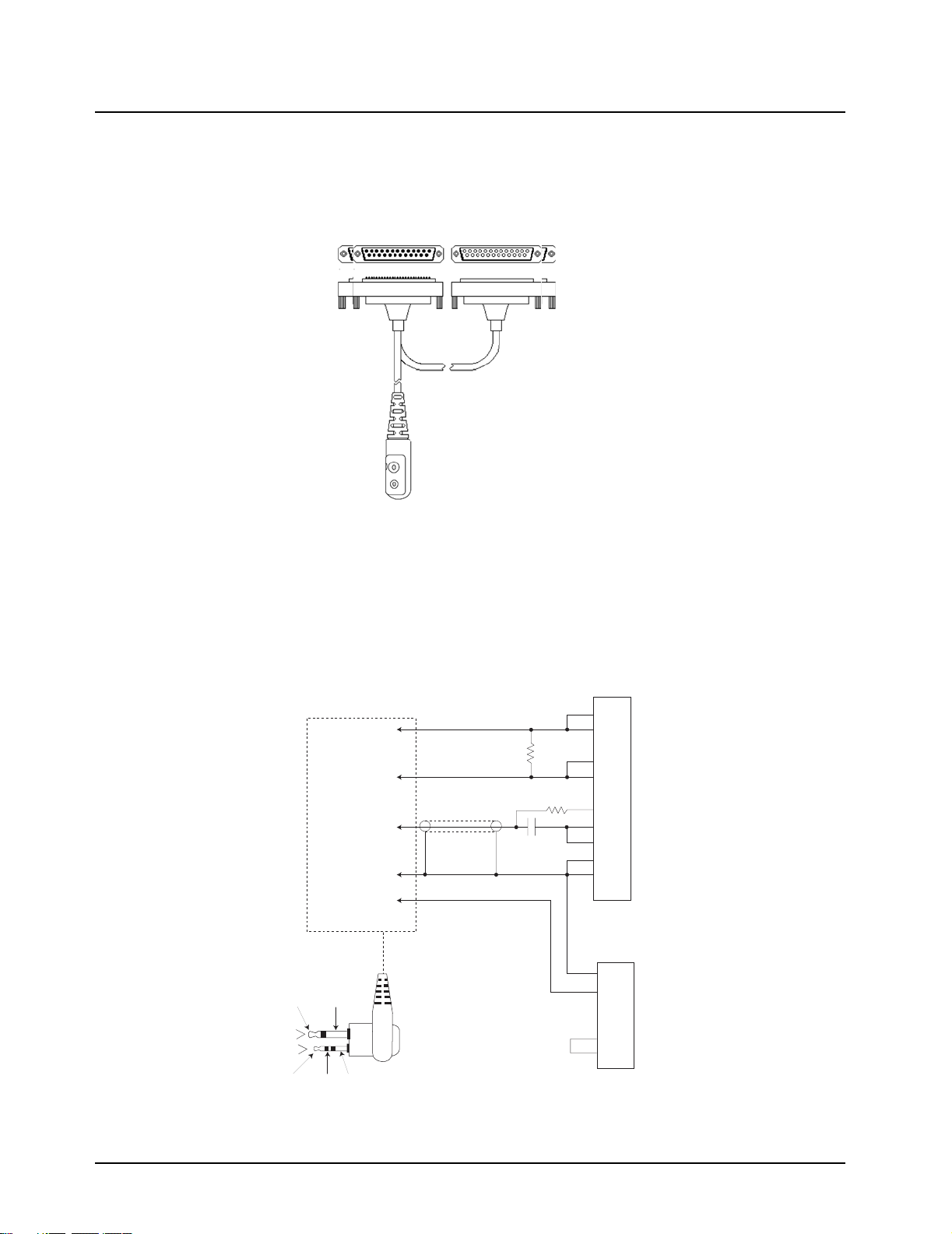
Figure 1-1. Programming/Test Cable...................... ... ... ... .... ... ... ... .... ... ... ... ... ......................................1-4
Figure 1-2. Wiring of the Connectors..................................................................................................1-4
Figure 2-1. DC Power Distribution Block Diagram..............................................................................2-1
Figure 4-1. VHF Receiver Block Diagram...........................................................................................4-1
Figure 4-2. VHF Transmitter Block Diagram.......................................................................................4-3
Figure 4-3. VHF Frequency Generation Unit Block Diagram..............................................................4-5
Figure 4-4. VHF Synthesizer Block Diagram ......................................................................................4-6
Figure 4-5. VHF VCO Block Diagram.............. ... .... ... ... ... .... ... ... ... .... ... ... ... ... .... ... ... ............................4-7
Figure 5-1. VHF Receiver Block Diagram...........................................................................................5-1
Figure 5-2. VHF Transmitter Block Diagram.......................................................................................5-3
Figure 5-3. VHF Frequency Generation Unit Block Diagram..............................................................5-5
Figure 5-4. VHF Synthesizer Block Diagram ......................................................................................5-6
Figure 5-5. VHF VCO Block Diagram.............. ... .... ... ... ... .... ... ... ... .... ... ... ... ... .... ... ... ............................5-7
Figure 7-1. Six-Layer Circuit Board: Copper Steps in Layer Sequence..............................................7-3
Figure 7-2. Speaker and Microphone Schematic................................................................................7-3
Figure 7-3. VHF (136-162 MHz) Radio Circuit Block Interconnect Diagram (8486769Z02-A) ...........7-5
Figure 7-4. VHF (136-162 MHz) Receiver Front End Schematic Diagram (8486769Z02-A)..............7-6
Figure 7-5. VHF (136-162 MHz) Receiver Back End Schematic Diagram (8486769Z02-A) .. ... .... ... ..7-7
Figure 7-6. VHF (136-162 MHz) Synthesizer Schematic Diagram (8486769Z02-A)..........................7-8
Figure 7-7. VHF (136-162 MHz) Voltage Controlled Oscillator Schematic
Diagram (8486769Z02-A).................................................................................................7-9
Figure 7-8. VHF (136-162 MHz) Transmitter and Power Control Schematic
Diagram (8486769Z02-A)..................................... ... ... .... ... ... ... .......................................7-10
Figure 7-9. VHF (136-162 MHz) Controller Interconnect Schematic Diagram (8486769Z02-A)......7-11
Figure 7-10. VHF (136-162 MHz) Microprocessor Circuitry Schematic Diagram (8486769Z02-A)...7-12
Figure 7-11. VHF (136-162 MHz) Audio Circuitry Schematic Diagram (8486769Z02-A) ......... ... .... ...7-13
Figure 7-12. VHF (136-162 MHz) DC Regulation Schematic Diagram (8486769Z02-A) ...................7-14
Figure 7-13. VHF (136-162 MHz) Board Top Side View (8486769Z02-A) .........................................7-15
Figure 7-14. VHF (136-162 MHz) Board Bottom Side View (8486769Z02-A) ....................................7-16
Figure 7-15. VHF (136-162 MHz) Radio Circuit Block Interconnect Diagram (8486769Z04-C) .........7-21
Figure 7-16. VHF (136-162 MHz) Receiver Front End Schematic Diagram (8486769Z04-C)............7-22
Figure 7-17. VHF (136-162 MHz) Receiver Back End Schematic Diagram (8486769Z04-C)............7-23
Figure 7-18. VHF (136-162 MHz) Synthesizer Schematic Diagram (8486769Z04-C)........................7-24
Figure 7-19. VHF (136-162 MHz) Voltage Controlled Oscillator Schematic
Diagram (8486769Z04-C)...............................................................................................7-25
Figure 7-20. VHF (136-162 MHz) Transmitter and Power Control Schematic
Diagram (8486769Z04-C)........................... ............................................. .... ...................7-26
Figure 7-21. VHF (136-162 MHz) Controller Interconnect Schematic Diagram (8486769Z04-C)......7-27
Figure 7-22. VHF (136-162 MHz) Microprocessor Circuitry Schematic Diagram (8486769Z04-C)....7-28
Figure 7-23. VHF (136-162 MHz) Audio Circuitry Schematic Diagram (8486769Z04-C) ...................7-29
Figure 7-24. VHF (136-162 MHz) DC Regulation Schematic Diagram (8486769Z04-C) ...................7-30
Figure 7-25. VHF (136-162 MHz) Board Component Side View (8486769Z04-C).............................7-31
Figure 7-26. VHF (136-162 MHz) Board Solder Side View (8486769Z04-C).....................................7-32
Figure 7-27. VHF (146-174 MHz) Radio Circuit Block Interconnect Diagram (8486342Z09-A) .........7-21
Figure 7-28. VHF (146-174 MHz) Receiver Front End Schematic Diagram (8486342Z09-A)............7-22
Figure 7-29. VHF (146-174 MHz) Receiver Back End Schematic Diagram (8486342Z09-A) ............7-23
Figure 7-30. VHF (146-174 MHz) Synthesizer Schematic Diagram (8486342Z09-A)........................7-24
Figure 7-31. VHF (146-174 MHz) Voltage Controlled Oscillator Schematic
Diagram (8486342Z09-A)...............................................................................................7-25
Figure 7-32. VHF (146-174 MHz) Transmitter and Power Control Schematic
Diagram (8486342Z09-A)..................................... ... ... .... ... ... ... .......................................7-26
June, 2005 6880309N62-C
Page 11

Table of Contents ix
Figure 7-33. VHF (146-174 MHz) Controller Interconnect Schematic Diagram ( 8486342Z09-A)...... 7-27
Figure 7-34. VHF (146-174 MHz) Microprocessor Circuitry Schematic Diagram (8486342Z09-A)...7-28
Figure 7-35. VHF (146-174 MHz) Audio Circuitry Schematic Diagram (8486342Z09-A) ...................7-29
Figure 7-36. VHF (146-174 MHz) DC Regulation Schematic Diagram (8486342Z09-A) ...................7-30
Figure 7-37. VHF (146-174 MHz) Board Component Side View (8486342Z09-A).............................7-31
Figure 7-38. VHF (146-174 MHz) Board Solder Side View (8486342Z09-A).....................................7-32
Figure 7-39. VHF (146-174 MHz) Radio Circuit Block Interconnect Diagram (8486342Z13-C).........7-37
Figure 7-40. VHF (146-174 MHz) Receiver Front End Schematic Diagram (8486342Z13-C) ...........7-38
Figure 7-41. VHF (146-174 MHz) Receiver Back End Schematic Diagram (8486342Z13-C)............7-39
Figure 7-42. VHF (146-174 MHz) Synthesizer Schematic Diagram (8486342Z13-C)........................ 7-40
Figure 7-43. VHF (146-174 MHz) Voltage Controlled Oscillator Schematic
Diagram (8486342Z13-C) .............................................................................................. 7-41
Figure 7-44. VHF (146-174 MHz) Transmitter and Power Control Schematic
Diagram (8486342Z13-C) .............................................................................................. 7-42
Figure 7-45. VHF (146-174 MHz) Controller Interconnect Schematic Diagram ( 8486342Z13-C)...... 7-43
Figure 7-46. VHF (146-174 MHz) Microprocessor Circuitry Schematic Diagram (8486342Z13-C)...7-44
Figure 7-47. VHF (146-174 MHz) Audio Circuitry Schematic Diagram (8486342Z13-C)...................7-45
Figure 7-48. VHF (146-174 MHz) DC Regulation Schematic Diagram (8486342Z13-C)................... 7-46
Figure 7-49. VHF (146-174 MHz) Board Component Side View (8486342Z13-C).............................7-47
Figure 7-50. VHF (146-174 MHz) Board Solder Side View (8486342Z13-C)..................................... 7-48
Figure 7-52. VHF (146-174 MHz) Radio Circuit Block Interconnect Diagram (8486769Z04-C).........7-53
Figure 7-53. VHF (146-174 MHz) Receiver Front End Schematic Diagram (8486769Z04-C) ...........7-54
Figure 7-54. VHF (146-174 MHz) Receiver Back End Schematic Diagram (8486769Z04-C)............7-55
Figure 7-55. VHF (146-174 MHz) Synthesizer Schematic Diagram (8486769Z04-C)........................ 7-56
Figure 7-56. VHF (146-174 MHz) Voltage Controlled Oscillator Schematic
Diagram (8486769Z04-C) .............................................................................................. 7-57
Figure 7-57. VHF (146-174 MHz) Transmitter and Power Control Schematic
Diagram (8486769Z04-C) .............................................................................................. 7-58
Figure 7-58. VHF (146-174 MHz) Controller Interconnect Schematic Diagram ( 8486769Z04-C)...... 7-59
Figure 7-59. VHF (146-174 MHz) Microprocessor Circuitry Schematic Diagram (8486769Z04-C)...7-60
Figure 7-60. VHF (146-174 MHz) Audio Circuitry Schematic Diagram (8486769Z04-C)...................7-61
Figure 7-61. VHF (146-174 MHz) DC Regulation Schematic Diagram (8486769Z04-C)................... 7-62
Figure 7-62. VHF (146-174 MHz) Board Component Side View (8486769Z04-C).............................7-63
Figure 7-63. VHF (146-174 MHz) Board Solder Side View (8486769Z04-C)..................................... 7-64
Figure 8-1. UHF Receiver Block Diagram .......................................................................................... 8-1
Figure 8-2. UHF Transmitter Block Diagram ...................................................................................... 8-3
Figure 8-3. UHF Frequency Generation Unit Block Diagram ............................................................. 8-5
Figure 8-4. UHF Synthesizer Block Diagram...................................................................................... 8-6
Figure 8-5. UHF VCO Block Diagram................................................................................................. 8-7
Figure 9-1. UHF Receiver Block Diagram .......................................................................................... 9-1
Figure 9-2. UHF Transmitter Block Diagram ...................................................................................... 9-3
Figure 9-3. UHF Frequency Generation Unit Block Diagram ............................................................. 9-5
Figure 9-4. UHF Synthesizer Block Diagram...................................................................................... 9-6
Figure 9-5. UHF VCO Block Diagram................................................................................................. 9-7
Figure 10-1. UHF Receiver Block Diagram ........................................................................................10-1
Figure 10-2. UHF Transmitter Block Diagram .................................................................................... 10-3
Figure 10-3. UHF Frequency Generation Unit Block Diagram ...........................................................10-5
Figure 10-4. UHF Synthesizer Block Diagram....................................................................................10-6
Figure 10-5. UHF VCO Block Diagram...............................................................................................10-7
Figure 12-1. Six-Layer Circuit Board: Copper Steps in Layer Sequence ........................................... 12-3
Figure 12-2. Speaker and Microphone Schematic .............................................................................12-3
Figure 12-3. UHF (403-440 MHz) Radio Circuit Block Diagram (8486635Z03-O) ......... ...... ... .... ... ... . 12-5
Figure 12-4. UHF (403-440 MHz) Receiver Front End Schematic Diagram (8486635Z03-O)........... 12-6
Figure 12-5. UHF (403-440 MHz) Receiver Back End Schematic Diagram (8486635Z03-O) ...........12-7
6880309N62-C June, 2005
Page 12

x Table of Contents
Figure 12-6. UHF (403-440 MHz) Synthesizer Schematic Diagram (8486635Z03-O) .......................12-8
Figure 12-7. UHF (403-440 MHz) Voltage Controlled Oscillator Schematic
Diagram (8486635Z03-O) ..............................................................................................12-9
Figure 12-8. UHF (403-44 0 MH z) Trans mit te r an d Pow er Cont ro l Sche m atic
Diagram (8486635Z03-O) ....................................... ... .... ... ... ... ... .... ... ... ... .....................12-10
Figure 12-9. UHF (403-440 MHz) Controller Interconnect Schematic Diagram (8486635Z03-O)....12-11
Figure 12-10. UHF (403-440 MHz) Microprocessor Circuitry Schematic Diagram (8486635Z03-O) 12-12
Figure 12-11. UHF (403-440MHz) Audio Circuitry Schematic Diagram (8486635Z03-O)..................12-13
Figure 12-12. UHF (403-440 MHz) DC Regulation Schematic Diagram (8486635Z03-O).................12-14
Figure 12-13. UHF (403-440 MHz) Board Component Side View (8486635Z03-O) ..........................12-15
Figure 12-14. UHF (403-440 MHz) Board Solder Side View (8486635Z03-O)...................................12-16
Figure 12-15. UHF (438-470 MHz) Radio Circuit Block Diagram (8486348Z09-A)............................12-21
Figure 12-16. UHF (438-470 MHz) Receiver Front End Schematic Diagram (8486348Z09-A)..........12-22
Figure 12-17. UHF (438-470 MHz) Receiver Back End Schematic Diagram (8486348Z09-A)..........12-23
Figure 12-18. UHF (438-470 MHz) Synthesizer Schematic Diagram (8486348Z09-A)......................12-24
Figure 12-19. UHF (438-470 MHz) Voltage Controlled Oscillator Schematic
Diagram (8486348Z09-A).............................................................................................12-25
Figure 12-20. UHF (438-470 MHz) Transmitter and Power Control Schematic
Diagram (8486348Z09-A)..................................... ... ... .... ... ... ... .....................................12-26
Figure 12-21. UHF (438-470 MHz) Controller Interconnect Schematic Diagram (8486348Z09-A)....12-27
Figure 12-22. UHF (438-470 MHz) Microprocessor Circuitry Schematic Diagram (8486348Z09-A) .12-28
Figure 12-23. UHF (438-470 MHz) Audio Circuitry Schematic Diagram (8486348Z09-A) .................12-29
Figure 12-24. UHF (438-470 MHz) DC Regulation Schematic Diagram (8486348Z09-A) .................12-30
Figure 12-25. UHF (438-470 MHz) Board Component Side View (8486348Z09-A)...........................12-31
Figure 12-26. UHF (438-470 MHz) Board Solder Side View (8486348Z09-A)...................................12-32
Figure 12-27. UHF (438-470 MHz) Radio Circuit Block Diagram (8486348Z13-C)............................12-37
Figure 12-28. UHF (438-470 MHz) Receiver Front End Schematic Diagram (8486348Z13-C) ........ .12-38
Figure 12-29. UHF (438-470 MHz) Receiver Back End Schematic Diagram (8486348Z13-C)..........12-39
Figure 12-30. UHF (438-470 MHz) Synthesizer Schematic Diagram (8486348Z13-C)......................12-40
Figure 12-31. UHF (438-470 MHz) Voltage Controlled Oscillator Schematic
Diagram (8486348Z13-C).............................................................................................12-41
Figure 12-32. UHF (438-470 MHz) Transmitter and Power Control Schematic
Diagram (8486348Z13-C)........................... ............................................. .... .................12-42
Figure 12-33. UHF (438-470 MHz) Controller Interconnect Schematic Diagram (8486348Z13-C)....12-43
Figure 12-34. UHF (438-470 MHz) Microprocessor Circuitry Schematic Diagram (8486348Z13-C).12-44
Figure 12-35. UHF (438-470 MHz) Audio Circuitry Schematic Diagram (8486348Z13-C).................12-45
Figure 12-36. UHF (438-470 MHz) DC Regulation Schematic Diagram (8486348Z13-C).................12-46
Figure 12-37. UHF (438-470 MHz) Board Component Side View (8486348Z13-C)...........................12-47
Figure 12-38. UHF (438-470 MHz) Board Solder Side View (8486348Z13-C)...................................12-48
Figure 12-39. UHF (465-495 MHz) Radio Circuit Block Diagram (8486634Z02-O)............................12-53
Figure 12-40. UHF (465-495 MHz) Receiver Front End Schematic Diagram (8486634Z02-O) .........12-54
Figure 12-41. UHF (465-495 MHz) Receiver Back End Schematic Diagram (8486634Z02-O)..........12-55
Figure 12-42. UHF (465-495 MHz) Synthesizer Schematic Diagram (8486634Z02-O) .....................12-56
Figure 12-43. UHF (465-495 MHz) Voltage Controlled Oscillator Schematic
Diagram (8486634Z02-O) ............................................................................................12-57
Figure 12-44. UHF (465-495 MHz) Transmitter and Power Control Schematic
Diagram (8486634Z02-O) ....................................... ... .... ... ... ... ... .... ... ... ... .....................12-58
Figure 12-45. UHF (465-495 MHz) Controller Interconnect Schematic Diagram (8486634Z02-O)....12-59
Figure 12-46. UHF (465-495 MHz) Microprocessor Circuitry Schematic Diagram (8486634Z02-O) 12-60
Figure 12-47. UHF (465-495 MHz) Audio Circuitry Schematic Diagram (8486634Z02-O).................12-61
Figure 12-48. UHF (465-495 MHz) DC Regulation Schematic Diagram (8486634Z02-O).................12-62
Figure 12-49. UHF (465-495 MHz) Board Component Side View (8486634Z02-O) ..........................12-63
Figure 12-50. UHF (465-495 MHz) Board Solder Side View (8486634Z02-O)...................................12-64
June, 2005 6880309N62-C
Page 13

Table of Contents xi
List of Tables
Table 1-1. Recommended Test Equipment.......................................................................................1-1
Table 1-2. Service Aids ..................................................................................................................... 1-2
Table 1-3. Recommended Service Tools.......................................................................................... 1-2
Table 2-1. Voltage Regulators........................................................................................................... 2-2
Table 3-1. Radio Memory Requirements........................................................................................... 3-1
Table 3-2. SPI Bus Signal Definitions................................................................................................ 3-2
Table 6-1. Troubleshooting Table for Receiver................................................................................. 6-1
Table 6-2. Troubleshooting Table for Synthesizer............................................................................. 6-3
Table 6-3. Troubleshooting Table for Transmitter............................................................................. 6-4
Table 6-4. Troubleshooting Table for Board and IC Signals ............................................................. 6-7
Table 11-1. Troubleshooting Table for Receiver............................................................................... 11-1
Table 11-2. Troubleshooting Table for Synthesizer...........................................................................11-3
Table 11-3. Troubleshooting Table for Transmitter........................................................................... 11-4
Table 11-4. Troubleshooting Table for Board and IC Signals ........................................................... 11-6
Related Publications
CP150/CP200 Basic Service Manual .............................................................................................6880309N61
CP150/CP200 User Guide..............................................................................................................6880309N60
6880309N62-C June, 2005
Page 14

xii Table of Contents
June, 2005 6880309N62-C
Page 15
Chapter 1 Test Equipment, Service Aids, and
Service Tools
1.1 Test Equipment
Table 1-1 lists test equipment required to service the CP150/CP200 Radios.
Table 1-1. Recommended Test Equipment
Motorola Part No. Description Characteristics Application
R2600 series System analyzer This item will substitute for
items with an asterisk (*)
*R1074A Fluke 87 digital multi-
meter
Fluke 85 RF probe 500 MHz, 30 VAC max Use with Fluke 87 digital multi-
*R1377A AC voltmeter 1 mV to 300 mV, 10 mega-
R1611A Dual channel
100 MHz oscilloscope (Agillent)
S1339A RF millivolt meter 100 µV to 3V RF, 10 kHz to
*R1013B or
*R1370A
SINAD meter or
SINAD meter with
RMS
True RMS metering,
200 kHz frequency
counter, 32-segment bar
graph with backlit display
ohm input impedance
Two-channel, 100 MHz
bandwidth, 200 M sample
rate/sec, 2 MB memory/
channel
1 GHz frequency range
Without RMS audio voltmeter or
With RMS audio voltmeter
Frequency/deviation meter and
signal generator for wide-range
troubleshooting and alignment
Digital voltmeter is recommended for AC/DC voltage and
current measurements
meter for RF voltage measurements.
Audio voltage measurements
Waveform measurements
RF level measurements
Receiver sensitivity measurements
Page 16
1-2 Test Equipment, Service Aids, and Service Tools: Service Aids
1.2 Service Aids
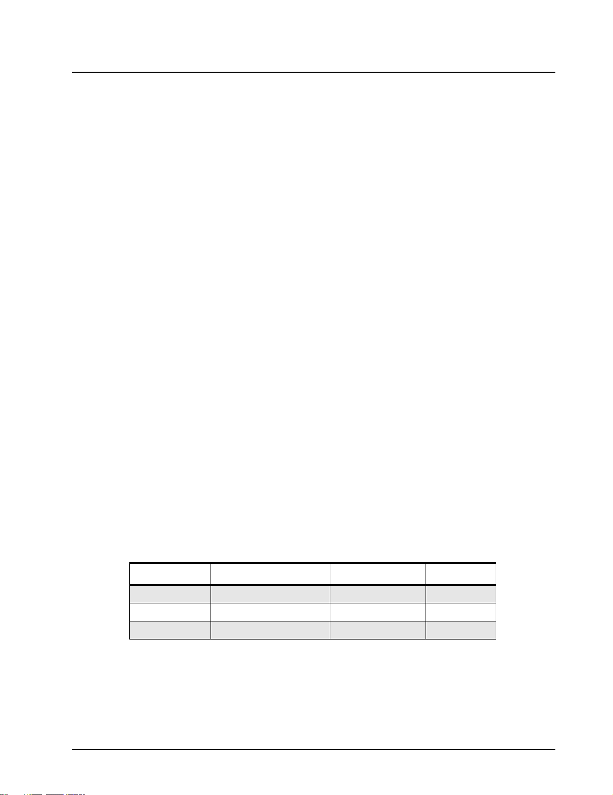
Table 1-2 lists service aids recommended for working on the CP150/CP200 Radios. While all of these
items are available from Motorola, most are standard shop equipment items, and any equivalent item
capable of the same performance may be substituted for the item listed.
Table 1-2. Service Aids
Motorola Part
No.
RLN4460 Por table Test Set Enables connection to the audio/accessory jack.
RLN4510 Battery Interface Regulates DC current and voltage between radio and
RVN4191 Customer Programming Soft-
ware and Global Tuner Software
on CD Rom
AAPMKN4004 Programming Test Cable Connects radio to RIB (PLN4008).
AAPMKN4003 Radio-to-Radio Cloning Cable
RLN4008 Radio Interface Box Enables communications between the radio and the
5886564Z01 RF Adaptor Adapts radio’s antenna port to BNC cabling of test
0180305K08 Shop Battery Eliminator Interconnects radio to power supply.
HSN9412 Wall-Mounted Power Supply Used to supply power to the RIB (120 VAC).
Description Application
Allows switching for radio testing.
power supply.
Program customer option and channel data.
Allows a radio to be duplicated from a master radio by
transferring programmed data from the master radio to
the other.
computer’s serial communications adapter.
equipment.
3080369B71 or
3080369B72
6686533Z01 Knob Remover/Chassis Opener Used to remove the front cover assembly.
HKN9216 IBM Computer Interface Cable Connection from computer to RIB.
8180384N65 Housing Eliminator Allows testing of the radio outside of the housing.
Motorola Part
No.
RSX4043A TORX screwdriver Tighten and remove chassis screws
6680387A70 T6 TORX bit Removable TORX screwdriver bit
R1453A Digital readout solder station Digitally controlled soldering iron
RLN4062A Hot air workstation, 120 V Tool for hot air soldering/desoldering of surface
Computer Interface Cable Use B72 for the IBM PC AT or newer (9-pin serial
port). Use B71 for older models (25-pin serial port).
Connects the computer’s serial communications
adapter to the RIB (PLN4008).
Table 1-3. Recommended Service Tools
Description Application
mounted integrated circuits
June, 2005 6880309N62-C
Page 17
Test Equipment, Service Aids, and Service Tools: Service Aids 1-3
Table 1-3. Recommended Service Tools (Continued)
Motorola Part
No.
Description Application
0180386A78 Illuminated magnifying glass with
lens attachment
Illumination and magnification of components
0180302E51 Master lens system
0180386A82 Anti-static grounding kit Used during all radio assembly and disassembly pro-
cedures
6684253C72 Straight prober
6680384A98 Brush
1010041A86 Solder (RMA type), 63/67,
0.5mm diameter, 1 lb. spool
0180303E45 SMD tool kit (included with
R1319A)
R1319A ChipMaster (110 V) Surface mount removal and assembly of surface
R1321A ChipMaster (220 V)
mounted integrated circuits and/or rework station
shields. Includes 5 nozzles.
ChipMaster Nozzles:
6680332E83 PLCC-28* nozzle
6680332E82 PLCC-44* nozzle
6680332E94 PLCC-52 nozzle
6680332E96 PLCC-84 nozzle
6680334E67 QFP-160 nozzle
6680333E46 SOL-18 nozzle
6680332E84 SOIC-20 nozzle
6680332E87 SOL-20J nozzle
6680333E45 SOL-24 nozzle
6680333E55 TSOP-64 nozzle
* Included with ChipMaster packages
Soldering and Un-soldering IC’s
6880309N62-C June, 2005
Page 18
1-4 Test Equipment, Service Aids, and Service Tools: Service Aids
Programming/Test Cable
3.5mm mono
2.5mm stereo
Figure 1-1. Programming/Test Cable
P1
2.5mm stereo and
3.5mm
3.5mm Tip
(Speaker +)
3.5mm
Sleeve
2.5mm Tip
(Microphone)
2.5mm
2.5mm
Center
1
2
5
3
4
25 POSITION
MALE CONNECTOR
P2 P3
36.0”
CABLE
P1
Orange
1
Blue
2
White
25 POSITION
FEMALE CONNECTOR
36.0”
CABLE
ohm
5
1UF,16V 5%
Spiral
3
Yellow
4
25 pin Male D Connector
P2
Components molded inside
1
5
47
24
7
33K
20
8
+
15
16
9
P3
25 pin Female
D Connector
1
15
4
11
To Test Box
To Test Box
Figure 1-2. Wiring of the Connectors
June, 2005 6880309N62-C
Page 19
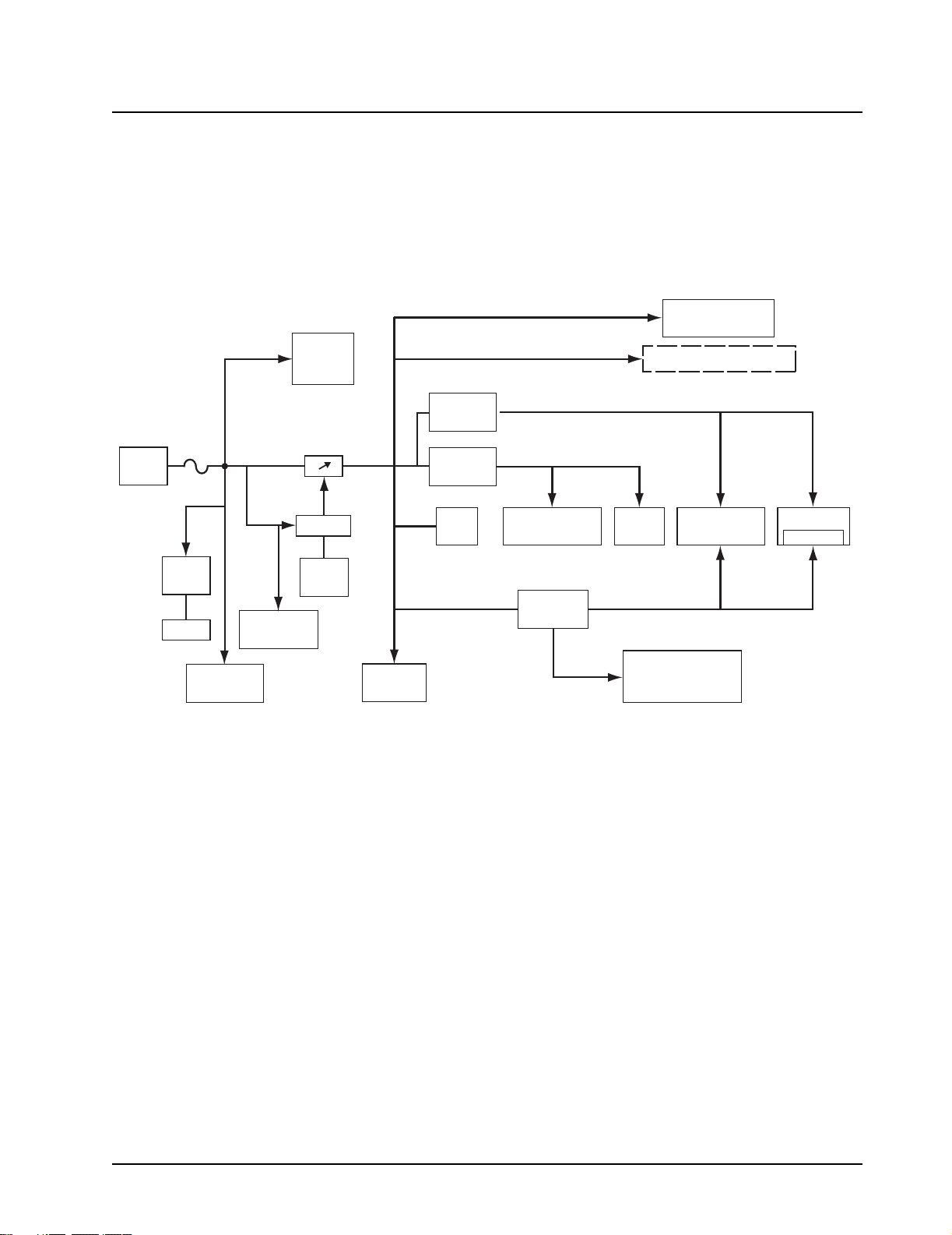
Chapter 2 DC Power Distribution
2.1 DC Regulation and Distribution
A block diagram of the DC power distribution throughout the radio is shown in Figure 2-1.
Audio
Power
Amplifier
Accessories
20 pin Connector
Keypad/Option Board
7.5V
Battery
5V
5V
Vdda
Vddd
LCD
Driver
RF AMP, IF AMP,
ASFIC_CMP
RX/TX Buffers
IFIC
FRACTN
VCOBIC
UNSWB+
Fuse
3.3V
Reg.
LI Ion
PA, Driver
PCIC(ALC)
MECH.
SWB+
Low Battery
Detect
Control
On/Off
Switch
SWB+
Antenna
Switch
Vdda
Regulator
Vddd
Regulator
Tx
Led
MCU, ROM
and EEPROM
Regulator
Figure 2-1. DC Power Distribution Block Diagram
Battery voltage enters at connector J301 and is routed through fuse F301 to become USWB+.
VR301 protects against ESD, and D301 provides reverse polarity protection. This voltage is routed
to:
• FET switch Q170 in the TX power control circuit (turned on during transmit)
• TX power amplifier module U110 (via R150)
• input pins of regulators U310, U320 and U330
• FET switch Q493 (turned on whenever the radio is on)
• on-off switch S444 (part of on-off-volume control) to become SWB+
Page 20
2-2 DC Power Distribution: DC Regulation and Distribution
When the radio is turned on, SWB+ is present and is applied to:
• transistor switch Q494 (pins 1 and 6) which turns on Q4 93
• RX audio power amplifier U490
• voltage divider R420/R421 and port PE0, a microprocessor A/D input which measures battery
voltage and radio on/off status
The output of FET switch Q493 is applied to the control pins of regulators U310, U320 and U330,
turning them on. The following regulators are used:
Table 2-1. Voltage Regulators
Reference No. Description Type
U310 5 V Regulator TK71750S
U320 Digital 3.3 V Regulator LP2986
U330 3 V Regulator TK71730S
The 5 V source is applied to:
• RX back end circuitry
• synthesizer super filter input and charge pump supply
• RED/GRN LEDs
• RX audio buffer U510
• portions of ASFIC U451
The 5 V source is also applied to FET switches Q311 and Q312. Q311 is turned on by Q313 when
RX_ENA (from U401 pin 49) is high, and supplies the "5R" source to the RF front end stages Q21Q22, and the VCO RX injection buffer Q280. Q312 is turned on by Q313 when TX_ENA (from U40 1
pin 50) is high, and supplies the "5T" source to the first transmitter stage Q100.
The digital 3.3 volt source from U320 (D_3.3 V) is applied to:
• microprocessor U401
• EEPROM U402
• flash ROM U404
The 3 V regulated source from U330 is applied to:
• synthesizer IC U201
• VCO/buffer IC U251
• portions of ASFIC U451
• microphone bias circuitry
While the radio is turned on, port PH3 (U401 pin 44) is he ld high. When the radio is turn ed off, SWB+
is removed and port PE0 (U401 pin 67) goes low, initiating a power-down routine. Port PH3 (pin 44)
remains high, keeping the voltage regulators on via Q493 and Q494, until the operating state of the
radio has been stored in EEPROM and other turn-off data functions have been completed. PH3 then
goes low, turning off Q494 and Q493, and all regulated voltages are removed.
June, 2005 6880309N62-C
Page 21
Chapter 3 Controller Theory of Operation
3.1 Controller
The controller provides the following functions:
• interface with controls and indicators
• serial bus control of major radio circuit blocks
• encoding and/or decoding of selective signaling formats such as PL, DPL , MDC1200 a nd QuikCall II
• interface to CPS programming via the microphone connector
• storage of customer-specific information such as channel frequencies, scan lists, and signaling
codes
• storage of factory tuning parame ters such as tra nsmitter powe r and de viation, r eceiver squelch
sensitivity, and audio level adjustments
• power-up, power-down and reset routines
Figure 7-3 (VHF) shows the interconnection between the controller and the various other radio
blocks. Figure 7-9 show the connections between the following circuit areas which comprise the
controller block:
• microprocessor circuitry
• audio circuitry
• DC regulation circuitry (refer to Chapter 2, DC Regulations and Distribution.)
• rotary and pushbutton controls and switches
• option board interface
The majority of the circuitry described below is contained in the (VHF) Mi croprocessor Circuitry
schematic diagrams (Figure 7-10). Portions are also found in the Audio and DC Regulation
schematics (Figures 7-11 and 7-12).
3.1.1 Microprocessor Circuitry
The microprocessor circuitry includes microprocessor (U401) and associated EEPROM, S-RAM (not
used in PR400 models), and Flash ROM memories. The following memory IC's are used:
Table 3-1. Radio Memory Requirements
Reference No. Description Type Size
U402 Serial EEPROM AT25128 16K x 8
U403 Static RAM (not used)
U404 Flash ROM AT49LV001N_70 V 128K x 8
Page 22
3-2 Controller Theory of Operation: Controller
3.1.1.1 Memory Usage
Radio operation is controlled by software that is stored in external Flash ROM memory (U404).
Radio parameters and customer specific information is stored in external EEPROM (U402). The
operating status of the radio is maintained in RAM located within th e microprocessor . When the radio
is turned off, the operating status of the radio is written to EEPROM before operating voltage is
removed from the micropro cessor. See section “3.1.1.7 Microprocessor Power-Up, Power-Down and
Reset Routine” on page 3-3 for a discussion of the power-down routine.
Parallel communication with U403 and U404 is via:
• address lines A(0)-A(16), from U401 port F ADDR0-ADDR13 and port G XA14-XA16
• data lines D(0)-D(7), from U401 port C DATA0-DATA7
• chip-select for U403, from PH6 (U401 pin 41)
• chip-enable for U404, from PH7 (U401 pin 38)
• output enable for U404, from PA7 (U401 pin 86)
• write-enable for both U403 and U404, from PG7_R/W (U401 pin 4)
Serial communication with U402 is via:
• the SPI bus (see section “3.1.1.3 Serial Bus Control of Circuit Blocks” on page 3-2)
• chip-select for U402, from PD6 (U401 pin 3)
3.1.1.2 Control and Indicator Interface
Ports PI3 and PI4 are outputs which control the top-mounted LED indicator. When PI3 is high, the
indicator is red. When PI4 is high, the indicator is green. When both are high, the indicator is amber.
When both are low, the indicator is off.
Pressing the side-mounted PTT button (S441) provides a lo w to port PJ0 (U401 pin 71), which
indicates PTT is asserted. Side-mounted option buttons 1 and 2 (S442 and S443) are connected to
Ports PJ6 (pin 77) and PJ7 (pin 78), respectively.
3.1.1.3 Serial Bus Control of Circuit Blocks
The microprocessor communicates with other circuit blocks via a SPI (serial peripheral interface) bus
using ports PD2 (data into uP), PD3 (data out of uP) and PD4 (clock). The signal names and
microprocessor ports are defined in Table 3-2.
Table 3-2. SPI Bus Signal Definitions
Signal Name Microprocessor Port Microprocessor Pin
SPI-DATA_IN PD2-MISO U401 Pin 99
SPI_DATA_OUT PD3-MOSI U401 pin 100
SPI_CLK PD4-SCK U401 pin 1
These signals are routed to:
• the audio filter IC (U451) to control internal functions such as gain change betwee n 25 kHz and
12.5 kHz channels, transmit or receive mode, volume adjustment, etc.
• the synthesizer IC U201 to load receive and transmit channel frequencies
• option board connector J460-1 for internal option configuration and control
• serial EEPROM U402 (both SPI_DATA_IN and SPI_DATA_OUT are used).
June, 2005 6880309N62-C
Page 23

Controller Theory of Operation: Controller 3-3
In order for each circuit block to respond only to the data intended for it, each peripheral has its o wn
chip select (or chip enable) line. The device will only respond to data when its enable line is pulled
low by one of the microprocessor ports, as follows:
• port PD5 (U401 pin 2) for the audio filter IC
• port PH0 (U401 pin 47) for the synthesizer IC
• port PD6 (U401 pin 3) for the serial EEPROM.
3.1.1.4 Interface to RSS Programming
The radio can be programmed, or the programmed information can be read, using a computer with
CPS (Customer Programming Software) connected to the radio via a RIB (radio interface box) or
with the RIB-less cable. Connection to the radio is made via the microphone connector (part of
accessory connector J471). The SCI line connects the programming contact (J471 pin 6) to ports
PD0_RXD (data into uP, pin 97) and PD1_TXD (data out of uP, pin 98). Transistor Q410 isolates the
input and output functions by allowing PD1 to pull the line low , but does not af fect incoming data from
being read by port PD0. This isolation allows high-speed 2-wire pr ogramm ing via TP401 and TP402
for factory programming and tuning.
3.1.1.5 S t orage of Customer-Specific Information
Information that has been programmed using CPS, such as channel frequencies or selective
signaling codes, are stored in the external EEPROM, where it is retained permanently (unless
reprogrammed) without needing DC power applied to the microprocessor.
3.1.1.6 Sensing of Externally-Connected Accessories
Port PJ1 is used to detect the presence of externally connecte d accessor ies. Port PJ1 (U401 pin 72)
is normally low, unless accessories (lapel speaker microphone, lightweight headset, etc.) are used
with the radio. This port is used to detect an accessory PTT or auto sensing of a VOX accessory.
If VOX is programmed into the radio channe l codeplug information, and PJ1 is high during power-u p,
the radio will activate VOX operation. If a low is present at port PJ1 during power-up, the radio will
use this port as an external PTT indicator.
3.1.1.7 Microprocessor Power-Up, Power-Down and Reset Routine
On power-up, the microprocessor is held in reset until the digital 3.3 V regulator (U320 pin 5)
provides a stable supply voltage. Once the dig ital supply reaches steady st ate and releases the re set
line (U320 pin 7), the microprocessor begins to start up. The ASFIC_CMP (U451) has already
started running and is providing the startup clock to the microprocessor. After reset release by all
circuits, the software within the microprocessor begins executing port assignments, RAM checking,
and initialization. A fixed delay of 100 ms is added to allow the audio circuitry to settle. Next, an alert
beep is generated and the steady state software begins to execute (buttons are read, radio circuits
are controlled).
When the radio is turned off, SWB+ is removed and port PE0 (U401 pin 67) goes low, initiating a
power-down routine. Port PH3 (pin 44) remains high, keeping the voltage regulators on via Q493
and Q494, until the operating state of the radio has been stored in EEPROM. PH3 then goes low,
and all regulated voltages are removed.
6880309N62-C June, 2005
Page 24

3-4 Controller Theory of Operation: Controller
The microprocessor reset line (pin 94) can be controlled directly by the digital 3.3 V regulator (U320
pin 7), the microphone jack (part of accessory connector J471) via Q472 and Q471, and the
microprocessor itself. U320 pulls the reset line low if the digital 3.3 V source loses regulation. This
prevents possible MOS latch-up or overwriting of registers in the microprocessor because the reset
line is higher in voltage than the microprocessor VDD ports (U401 pins 12, 39, 59, 88). The
microprocessor can drive the reset line low if it detects a fault condition such as an expired watchdog
timer, software attempting to execute an infinite loop, unplanned hardware inputs, static discharge,
etc. Finally, the Q471 can pull the reset line low during use of the programming cable and CPS by
the application of a sufficiently negative voltage to the microphone connector tip contact (J471 pin 4),
however this reset method is not utilized.
3.1.1.8 Boot Mode Control
When power-up reset occurs, the microprocessor will boot into either normal or flash mode
depending on the logic level of ports MODA (U401 pin 58) a nd MODB (pin 57). T he Flash Adapter is
a programming accessory which provides negative 9 volts dc via a 1K resistor to microphone
connector J471 pin 4. This turns on Q471 and Q472 via D471 and VR472, pulling MODA and MODB
low and allowing booting in the flash mode by cycling power to reset the radio. Software upgrades
can then performed by loading the new software code into Flash ROM U404.
3.1.1.9 Microprocessor 7.3975 MHz Clock
The 7.3975 MHz clock signal (uP_CLK) is provided from the ASFIC_CMP (U451 pin 28). Upon
startup the 16.8MHz crystal provides the signal to the ASFIC_CMP, which sends out the uP_CLK at
3.8MHz until a steady-state condition is reached and the clock is increased to 7.3975MHz for the
microprocessor.
3.1.1.10 Battery Gauge
Various battery types are available having different capacities. The different battery types contain
internal resistors connected from the BATT_CHARGE contact to ground (which is routed to the
microprocessor as BATT_DETECT). A voltage divider is formed with R255 pro ducing a different DC
voltage for each battery type, which is read by microprocessor port PE2 (pin 65). This allows the
software to recognize the battery chemistry being used and adjust the battery gauge fo r best
accuracy.
3.1.2 Audio Circuitry
3.1.2.1 Transmit and Receive Low-Level Audio Circuitry
The majority of RX and TX audio processing is performed by U451, the Audio Filter IC
(ASFIC_CMP), which provides the following functions:
• Tone PL/Digital PL encode and decode filtering
• Tone PL/Digital PL rejection filter in RX audio path
• TX pre-emphasis amplifier
• TX audio modulation limiter
• Post-limiter (splatter) filter
• TX deviation adjust (digitally-controlled attenuators)
• Programmable microphone gain attenuator
• RX audio volume control (digitally controlled attenuator)
• Carrier squelch adjustment (digitally controlled attenuator)
• Microprocessor output port expansion
June, 2005 6880309N62-C
Page 25

Controller Theory of Operation: Controller 3-5
• 2.5 volt dc reference source
• Microprocessor clock generation (from the 16.8 MHz reference oscillator input)
The parameters of U451 that are programmable are selected by the microprocessor via the CLOCK
(U451 pin 21), DATA (U451 pin 22) and chip enable (U451 pin 20) lines.
RX audio buffer U510 amplifies the audio level from the DEMOD output of the IFIC before being
applied to the audio filter IC input (DISC, U451 p in 2). The buffer is DC coupled to avoid corruption of
low-frequency data waveforms such as DPL. Because such waveforms are polarity sensitive, this
buffer is configured as a single-stage inverting amplifier (U510-1 only) for VHF models where highside first injection is used, or is configured as a two-stage non-inver ting amplifie r (U510-1 and -2 ) for
UHF models using low-side first injection. The gain of the buffer is 1.5 times or 3.5 dB.
U480 and associated components are not used. Stage U480-1 is bypassed by jumper R487.
Volume adjustment is performed by a digital attenuator within U451. The volume control (10KO, part
of S444) is connected to D_3.3 V and ground via R506 and R507. When the volume control is
rotated, it varies the dc volt age applie d to micr oprocessor A/D input por t PE1 (U4 01 pin 66) between
approximately 0 volts dc at minimum volume to 3.3 volts dc at maximum volume. Depending on this
voltage, the appropriate setting of the digital volume attenuator is selected. This technique is less
susceptible to noise than a conventional analog volume control.
3.1.2.2 Audio Power Amplifier
The audio power amplifier IC U490 amplifies receiver audio from U451 pin 41 to a level sufficient to
drive a loudspeaker. U490 is a bridge amplifier delivering 3.46 volts rms between pins 5 and 8
without distortion, which is sufficient to develop 500 milliwatts of audio power into the internal 24 ohm
speaker or an external 24 ohm load. The audio power amplifier is muted whenever speaker audio is
not required to reduce current drain. The audio amp is muted when U451 pin 14 is low. When U451
pin 14 is high, U490 pin 1 is pulled low by Q490, enabling the audio amplifier.
Because the power amplifier is a bridge-type, neither speaker terminal is gro unded. Care should be
taken that any test equipment used to measure the speaker audio voltage does not ground either
speaker output terminal, otherwise damage to the audio power amplifier IC may result. When a 24ohm load resistor is used it should be connected between the tip and the sleeve of accessory jack
J471 (3.5mm port), never to ground. External SPKR plug insertion mechanically disconnects the
internal speaker. Volta ge measurements using test equipment that is not isolated from ground may
be made from one side of the speaker or load r esistor (either the tip or the sle eve of J471) to chassis
ground, in which case the voltage indicated will be one half of the voltage applied to the speaker or
load resistor . The Motorola RLN44 60 Port able Test Set and AAPMKN4004 Programming T est Cable
provide the proper interface between the radio's ungrounded audio output and ground-referenced
test equipment.
3.1.2.3 Internal Microphone Audio Voice Path
Microphone audio from internal microphone is routed from J470-1 via C475, L471, and C470 to the
ASFIC_CMP mic audio input (MICINT, U451 pin 46). During transmit, Q470 is turned on by a low at
U451 pin 35, providing dc bias for the internal MIC via R478. External MIC plug insertion
mechanically disconnects the internal microphone. External MIC audio is coupled through L4 71 and
C470 to the mic audio input. An input level of 10 mV at J471 pin 4 produces 200 mV at the output of
U451 pin 40, which corresponds to 60% deviation.
6880309N62-C June, 2005
Page 26

3-6 Controller Theory of Operation: Controller
3.1.2.4 PTT Circuits
The internal side-mounted PTT switch (S441) is sensed directly by microprocessor port PJ0 (U401
pin 71). External mic PTT is sensed by measuring the current drawn through the accessory
connector (J471-4) by the mic cartridge (which is in series with the accessory PTT switch). This
current is drawn through the base (pin 5) and emitter (pin 4) of a transistor in Q470, causing its
collector (pin 3) to supply a logic-high to microprocessor port PJ1 (pin 72).
3.1.2.5 VOX Operation
VOX audio accessories do not have a PTT switch. Instead, the mic cartridge is wired directly from
J471-4 to ground. If the radio has been programmed for VOX operation an d the VOX accessory is
plugged in prior to turning the radio on, the current drawn by the cartridge will turn on Q470 (pins 34-5) and a logic high will be seen at port PJ1 at turn-on. The microprocessor then assumes VOX
operation, with PTT controlled by the presence of audio at the mic cartridge. A dc voltage
proportional to the audio level at the input of the ASFIC_CMP (U451 pin 46) is fed to a n A/D in put of
microprocessor U401 (pin 62). During VOX operation, PT T is activate d whe n the dc leve l exceeds a
preset threshold.
3.1.2.6 Battery Charging Through Microphone Jack
A wall-type charging power supply may be connected to the 2.5 mm microphone jack (p art of
accessory connector J451). The voltage present at the tip contact (pin 4) is app lied to the center
charging contact of the battery via diode D470. Another diode, internal to the battery, applies this
voltage to the (+) battery terminal. Only the recommended charger and battery type should be
charged in this manner.
Different battery types contain internal resistors connected from the BATT_CHARGE contact to
ground, which is routed to the microprocessor as BATT_DETECT. A voltage divider is formed with
R255 producing a DC voltage which is read by microprocessor port PE2 (pin 65). This allows the
software to recognize the battery chemistry being used and adjust the battery gauge fo r best
accuracy. The value of R255 is chosen so that the voltage at the BATT_CHARGE node (cathode of
D470) is never low enough to turn on the EXT_MIC_PTT sense transistor (part of Q470).
3.1.2.7 Programming and Flashing Through Microphone Jack
The ring contact on the 2.5 mm microphone jack is used for reading, pr ogramming or re-flashing the
radio using CPS. This contact (J471 pin 6) is routed to port s PD0_RXD (data into uP, pin 97) and
PD1_TXD (data out of uP, pin 98). Transistor Q410 isolates the input and output functions by
allowing PD1 to pull the line low, but does not affect incoming data from being read by port PD0.
To re-flash the radio (ov erw rit e th e software in the F lash ROM wi th ne w so ftware), the ra dio mu st
power up in the boot mode. This is accomplished by using a flash adapter acce ssory, which provides
SCI communication with the programming ring contact (J471 pin 6) and also allows a negative
voltage (negative 9 volts dc via a 1K resistor) to be applied to the tip contact (J471 pin 4). This
voltage is sufficient to turn on the base-emitter junction (pins 1 and 2) of Q472 via L471, D471,
VR472 and R471. Pin 6 of Q472 goes high, turning on Q471 (pins 3 and 4) and pulling the
BOOT_ENA line (ports MODA and MODB of the microprocessor) low. Cycling power generates a
reset which causes the radio to boot in the flash mode.
June, 2005 6880309N62-C
Page 27
Chapter 4 136-162 MHz VHF Theory Of Operation
4.1 Introduction
This chapter provides a detailed theory of operation for the radio components. Schematic diagrams
for the circuits described in the following paragraphs are located in Chapter 7 of this manual.
4.2 VHF Receiver
The VHF receiver covers the range of 136-162 MHz and provides switchable IF bandwidth for use
with 12.5 kHz or 20/25 kHz channel spacing systems. The receiver is divided into two major blocks as
shown in Figure 4-1.
•Front End
• Back End
Preselector
RX from
Antenna Switch
from Synthesizer
4.2.1 Receiver Front-End
Incoming RF signals from the antenna are first routed throug h the harmonic filter and ante nna switch,
part of the transmitter circuitry, before being applied to the receiver front end. The receiver front end
consists of a preselector filter, RF amplifier, an interstage filter, and a double-balanced first mixer.
The preselector filter is a fixed-tuned 4-pole design using discrete elements (L1-L4 and C1-C9) in a
series/shunt resonator configuration. It has a 3 dB bandwidth of 43 MHz, an in sertion loss of 2 dB and
image attenuation of 37 dB at 226 MHz, with increasing attenuation at higher frequencies. Diode CR1
protects the RF amplifier by limiting excessive RF levels.
The output of the filter is matched to the base of RF amplifier Q21, which provides 18 dB of gain and
a noise figure of 2 dB. Operating voltage is obtained from the 5R source, which is turned off during
transmit to reduce dissipation in Q21. Current mirror Q22 maintains the operating current of Q21
RF
Filter
First LO
Recovered Audio
Figure 4-1. VHF Receiver Block Diagram
Amp
RSSI
Interstage
Filter
Inj Filter
Ceramic
Resonator
1st Mixer
Demodulator
Crystal
Filter
6G
Switching
6E
IF
Amp
BW_SEL
Cer Fltr
4E
Page 28
4-2 136-162 MHz VHF Theory Of Operation: VHF Receiver
constant at 6.2 mA regardless of device and temperature variations, for optimum dynamic range and
noise figure.
The output of the RF amplifier is applied to the interstage filter, a fixed-tuned 3-pole series-coupled
resonator design having a 3 dB bandwidth of 54 MHz and insertion loss of 1.8 dB. This filter has an
image rejection of 40 dB at 226 MHz, with increasing attenuation at higher frequencies.
The output of the interstage filter is connected to the passive double-balanced mixer consisting of
components T41, T42, and CR41. This mixer has a conversion loss of 7 dB. High-side injection from
the frequency synthesizer is filtered by L40-L41 and C40-C44 to remove second harmonic energy
that may degrade half-IF spurious rejection performance. The injection filter has a 3 dB bandwidth of
52 MHz and an insertion loss of 1.5 dB. The filtered injection signal is applied to T42 at a level of +6
dBm.
The mixer output is applied to a diplexer network (L51-L52, C51, R51) which ma tches the 44 .85 MHz
IF signal to crystal filter FL51, and terminates the mixer into 50Ω at all other frequencies
4.2.2 Receiver Back-End
The receiver back end is a dual conversion design. High IF selectivity is provided by FL51, a 4-pole
fundamental mode 44.85 MHz crystal filter with a minimum 3 dB bandwidth of + 6.7 kHz, a maximum
20 dB bandwidth of ±12.5 kHz, and a maximum insertion loss of 3.5 dB. The output is matched to IF
amplifier stage Q51 by L53 and C93. Q5 1 provides 16 dB of gain and a noise figure of 1.8 dB. The dc
operating current is 1 mA. The output of Q51 is applied to the input of the receiver IFIC U51. Diode
CR51 limits the maximum RF level applied to the IFIC.
The IFIC is a low-voltage monolithic FM IF system incorporating a mixer/oscillator, two limiting IF
amplifiers, quadrature detector, logarithmic received signal strength indicator (RSSI), voltage
regulator and audio and RSSI op amps. The second LO frequency, 44.395 MHz, is determined by
Y51. The second mixer converts the 44.85 MHz high IF frequency to 455 kHz.
Additional IF selectivity is provided by two ceramic filters, FL52 (between the second mixer and IF
amp) and FL53 or FL54 (between the IF amp and the limiter input). The wider filter FL53 is used for
20/25 kHz channel spacing, and the narrower filter FL54 is used for 12.5 kHz channels. When the
BW_SEL line is high, the two upper diodes in packages D51 and D52 are forward biased, selecting
FL53 for 20/25 kHz channels. When the BW_SEL line is low, the two lower diodes in packages D51
and D52 are forward biased, selecting FL54 for 12.5 kHz channels.
FL52 FL53 FL54
Number of Elements: 4 6 6
Insertion Loss: 4 dB 4 dB 4 dB
6 dB Bandwidth: 15 kHz 15 kHz 9 kHz
50 dB Bandwidth: 30 kHz 30 kHz 22 kHz
Stopband Rejection: 27 dB 47 dB 47 dB
Ceramic resonator Y70 provides phase vs. frequency characteristic required by the quadrature
detector, with 90 degree phase shift occurring at 455 kHz. Buffer Q70 provides a lower driving
impedance from the limiter to the resonator, improving the IF waveform and lowering the distortion of
the recovered audio signal. The recovered audio level at the DEMOD output is 120 mV rms (25 kHz
channel, 3 kHz deviation) or 60 mV rms (12.5 kHz chan n el, 1. 5 kHz devia tio n) . An ad dit ion a l RSSI
output provides a DC voltage level that is proportio nal to RF signal level. This volt age is measured by
an A/D converter contained in the microprocessor (PE4_AN4, U401 pin 63).
June, 2005 6880309N62-C
Page 29
136-162 MHz VHF Theory Of Operation: VHF Transmitter 4-3
4.3 VHF Tr ansmitter
The VHF transmitter covers the range of 136-162 MH z. Depen ding on mo del, the output po wer of the
transmitter is either switchable on a per-channel basis between high power (5 watts) and low power
(1 watt), or is factory preset to 2 watts. The transmitter is divided into four major blocks as shown in
Figure 4-2.
• Power Amplifier
• Harmonic Filter
• Antenna Matching Network
• Power Control
USWB+
TX_INJ
(From VCO)
TX_ENA
PWR_SET
5T
Q100
Power Control
VGG
Power Amplifier Module U110
Figure 4-2. VHF Transmitter Block Diagram
4.3.1 Transmit Power Amplifier
The transmitter power amplifier has three stages of amplification. The first stage, Q100, operates in
Class AB from the 5T source. It provides 13 dB of gain and an output of 20 mW. The current drain is
typically 25mA. Components C105-C107 and L103 match the output of Q100 to the 50Ω input of the
module U110.
U110 is a two stage Silicon MOS FET power amplifier module. Drain voltage is obtained from UNSW
B+ after being routed through current-sense resistor R150 in the power control circuit. The output
power of the module is controlled by varying the DC gate bias on U110 pin 2 (VGG).
4.3.2 Antenna Switch
VDD
RX_IN
(To Receiver)
Antenna
Switch
Harmonic Filter
Antenna
Matching
Network
J140 Antenna
Jack
Antenna
The antenna switch consists of two pin diodes, D120 and D121. In the rece ive mode, both diodes are
off. Signals applied at the antenna or at jack J140 are routed, via the harmonic filter, through network
C122-C124 and L121, to the receiver input. In the transmit mode, Q170 is on and TXB+ is present,
forward-biasing both diodes into conduction. The diode current is 50 mA, set by R120-R122. The
transmitter RF from U110 is routed through D120, and via the harmonic filter to the antenna jack.
D121 conducts, shunting RF power and preventing it from reaching the receiver. L121 is selected to
appear as a 1/4 wave at VHF, so that the low impedance of D121 appears as a high impedance at the
junction of D120 and the harmonic filter input. This provides a high series impedance and low shunt
impedance divider between the power amplifier output and receiver input.
4.3.3 Harmonic Filter
The harmonic filter consists of components C130- C136 and L130-L132. The harmonic filter is a
seven-pole elliptical low-pass configuration, optimized for low insertion loss, with a 3 dB frequency of
approximately 180 MHz and typically less than 0.8 dB insertion loss in the passband.
6880309N62-C June, 2005
Page 30

4-4 136-162 MHz VHF Theory Of Operation: VHF Frequency Generation Circuitry
4.3.4 Antenna Matching Network
The harmonic filter presents a 50 Ω impedance to antenna jack J140. A matching network, made up
of C140-C141 and L140, is used to match the antenna impedance to the harmonic filter. This
optimizes the performance of the transmitter and receiver into the impedance presented by the
antenna, significantly improving the antenna's efficiency.
4.3.5 Power Control
The power control circuit is a dc-coupled amplifier whose output is the dc gate bias voltage (VGG)
applied to the two stages of the RF power amplifier U110.
The output power of the transmitter is adjusted by varying the setting of the power-set DAC cont ained
in the ASFICcmp IC (DACG, U451 pin 6). This PWR_SET voltage is applied to U150 pin 3.
Stage U150-2 compares the voltage drop across current sense resistor R150 to the voltage drop
across resistor R151 caused by current flow through Q150, and adjusts its output (pin 7) to maintain
equal voltages at pins 5 and 6. Thus the current flow through Q150, and hence its emitter voltage, is
proportional to the current drawn by stage U110, which is in turn proportional to the transmitter output
power. The emitter voltage of Q150 is applied to U150 pin 2, where it is compared to the power set
voltage PWR_SET at pin 3.
The output of U150 pin 1 is divided by R110 and R111 and applied as a gate voltage to the power
amplifier U110. By varying this gate voltage as needed to keep the voltages at U150 pins 2 and 3
equal, power is maintained at the desired setting. Excessive final current, for example due to antenna
mismatch, causes a lowering of the voltage at U150 pin 6, an increased voltage at pin 2, and a
lowering of the voltage at pin 1 and of the gate voltage VGG. This prevents damage to the final stage
due to excessive current.
4.4 VHF Frequency Generation Circuitry
The frequency generation system, shown in Figure 4-3, is composed of two circuit blocks, the
Fractional-N synthesizer IC U201, the VCO/Buffer IC U251, and associated circuitry. Figure 4-4
shows the peripheral interconnect and support circuitry used in the synthesizer block, and Figure 4-5
details the internal circuitry of the VCOBIC and its interconnections to the surrounding components.
Refer to the schematic to identify reference designators.
The Fractional-N synthesizer is powered by regulated 5 V and 3 V provided by U310 and U330
respectively. 5 V is applied to U201 pins 13 and 30, and 3 V is applied to pins 5, 20, 34 and 36. The
synthesizer in turn generates a super-filtered 4.5 V supply (VSF, from pin 28) to power U251. In
addition to the VCO, the synthesizer also interfaces with the logic and ASFICcmp circuits.
Programming for the synthesizer is accomplished through the microprocessor SPI_DATA_OUT,
SPI_CLK, and SYNTH_CS (chip select) lines (U409 pins 100, 1 and 47 respectively). A logic high
(3 V) from U201 pin 4 indicates to the microprocessor that the synthesizer is locked.
June, 2005 6880309N62-C
Page 31

136-162 MHz VHF Theory Of Operation: VHF Frequency Generation Circuitry 4-5
Transmit modulation from the ASFICcmp (U451 pin 40) is applied to U201 pin 10 (MOD_IN). An
electronic attenuator in the ASFICcmp adjusts overall transmitter deviation by varying the audio level
applied to the synthesizer IC. Internally the audio is digitized by the Fractional-N synthesizer and
applied to the loop divider to provide the low-port modulation. The audio is also routed through an
internal attenuator for the purpose of balancing the low port and high port modulation and reducing
the deviation by 6 dB for 12.5 kHz channels, and is available at U201 pin 41 (VCO_MOD). This audio
signal is routed to the VCO's modulator.
Voltage
Multiplier
VCP
Vmult1
Vmult2
Synthesizer
Aux3
U201
16.8 MHz
Ref. Osc.
MOD Out
Modulating
Signal
Figure 4-3. VHF Frequency Generation Unit Block Diagram
4.4.1 Fractional-N Synthesizer
The Fractional-N synthesizer, shown in Figure 4-4, uses a 16.8 MHz crystal (Y201) to provide the
reference frequency for the system. External components C201-C203, R202 and D201 are also part
of the temperature-compensated oscillator circuit. The dc voltage applied to varactor D201 from U201
pin 25 is determined by a temperature-compensation algorithm within U201, and is specific to each
crystal Y201, based on a unique code assigned to the crystal that identifies its temperature
characteristics. Stability is better than 2.5 ppm over temperatures of -30 to 60 °C. Softwareprogrammable electronic frequency adjustment is achieved by an internal DAC which provides a
frequency adjustment voltage from U201 pin 25 to varact or D201.
The synthesizer IC U201 further divides the 16.8 MHz signal to 2.1 MHz, 2.225 MHz, or 2.4 MHz for
use as reference frequencies. It also provides a buffered 16.8 MHz signal at U201 pin 19 for use by
the ASFICcmp.
To achieve fast locking of the synthesizer, an internal adapt charge pump provides higher current at
U201 pin 45 to quickly force the synthesizer within lock range. The required frequency is then locked
by the normal mode charge pump at pin 43. A lo op filter (C243 -C245 and R243 -R245) removes noise
and spurs from the steering voltage applied to the VCO varactors, with additional filtering located in
the VCO circuit.
Both the normal and adapt charge pumps get their supply from the capa citive volt age multiplie r made
up of C221-C224 and D220-D221. Two 3 V square waves from U201 pins 14-15 provide the drive
signals for the voltage multiplier, which generates 12.1 V at U201 pin 47. This voltage is filtered by
C225-C228.
Loop
Filter
TRB
Rx VCO
Circuit
Tx VCO
Circuit
VCOBIC
U251
Rx Out
Tx Out
Buffer
Q280
To Mixer
To PA Driver
6880309N62-C June, 2005
Page 32

4-6 136-162 MHz VHF Theory Of Operation: VHF Frequency Generation Circuitry
One of the auxiliary outputs of the synthesizer IC (AUX3, U201 pin 2) provides the TRB signal which
determines the operating mode of the VCO, either receive or transmit.
13,30
10
23
25
32
47
7
8
9
DATA
CLK
CEX
MODIN
V
, 5V
CC
, 3V
V
DD
XTAL1
WARP
PREIN
VCP
VMULT2
U201
Low Voltage
Fractional-N
Synthesizer
VMULT1
14
15
Prescaler In
DATA (U401 Pin 100)
CLOCK (U401 Pin 1)
SYNTH_CS (U401 Pin 47)
MOD IN (U451 Pin 40)
+5V (U310 Pin 5)
+3V (U330 Pin 5)
Reference
Oscillator
Voltage
Multiplier
5,20,34,36
Figure 4-4. VHF Synthesizer Block Diagram
4.4.2 Voltage Controlled Oscillator (VCO)
The VCOBIC (U251), shown in Figure 4-5, in conjunction with the Fractional-N synthesizer (U201)
generates RF in both the receive and the transmit modes of operation. The TRB line (U251 pin 19)
determines which oscillator and buffer are enabled. A sample of the RF signal from the enabled
oscillator is routed from U251 pin 12 through a low pass filter, to the prescaler input of the synthesizer
IC (U201 pin 32). After frequency comparison in the synthesizer, a resultant DC control voltage is
used to steer the VCO frequency. When the PLL is locked on frequency, this voltage can vary
between 3 V and 9 V. L251 and C251 further attenuate noise and spurs on the steering line voltage.
In the receive mode, the TRB line (U251 pin 19) is low. This activates the receive VCO and the
receive buffer of U251, which o perate within the ra nge of 180 .85 to 20 6.85 MHz. The VCO frequen cy
is determined by tank inductor L254, C253 -C257, and varactor D251. The buf fered RF signal at U251
pin 8 is further amplified by Q280 and applied as RX_INJ to the low-p ass injection filter in the receiver
front end circuit.
In the transmit mode, U251-19 is driven high by U201 pin 2, enabling the transmit VCO and buffer.
The 136-162 MHz RF signal from U251 pin 10 is applied as TX_INJ to the input of the transmitter
circuit via matching network C290-C291 and L291. TX VCO frequency is deter mined by L264, C263-
LOCK
FREFOUT
GND
IOUT
IADAPT
MODOUT
AUX3
SFOUT
BIAS1
BIAS2
4
19
6,22,23,24
43
45
41
2
28
40
39
LOCK (U401 Pin 56)
FREF (U451 Pin 34)
2-Pole
Loop Filter
VCO
TRB
Filtered 5V
Mod
Steering
Line
LO RF
Injection
Voltage
Controlled
Oscillator
TX RF
Injection
(First Stage of PA)
June, 2005 6880309N62-C
Page 33

136-162 MHz VHF Theory Of Operation: VHF Frequency Generation Circuitry 4-7
C267, and varactor D261. High-port audio modulation from the synthesizer IC is applied as
VCO_MOD to varactor D262 which modulates the transmit VCO.
AUX3 (U201 Pin 2)
TRB_IN
Steer Line
Voltage
(V_STEER)
NC
NC
V_SF (U201 Pin 28)
RX VCO
RX
TX
Circuit
TX VCO
Circuit
Tank
Tank
Pin 7
Pin 13
Pin 3
Pin 4
Pin 5
Pin 6
Pin 16
Pin 15
Pin 18
Vcc-Logic
Pin 20
Vcc-Superfilter
Collector/RF in
RX
TX
Vsens
Circuit
TX/RX/BS
Switching Network
U251
VCOBIC
Rx Active
Bias
Tx Active
Bias
Pin 2
Rx-I adjust
Pin 19
Pin 1
Tx-I adjust
Pin 12
Presc
Pin 8
RX
Pin 14
Pin 10
TX
Pins 9,11,17
Prescaler Out
Buffer
Q280
VCC Buffers
U201 Pin 32
RX INJ
3V (U330 Pin 5)
Matching
Network
TX INJ
3V
(U330 Pin 5)
(U201 Pin 28)
Figure 4-5. VHF VCO Block Diagram
V_SF
6880309N62-C June, 2005
Page 34

4-8 136-162 MHz VHF Theory Of Operation: VHF Frequency Generation Circuitry
Notes:
June, 2005 6880309N62-C
Page 35

Chapter 5 146-174 MHz VHF Theory Of Operation
5.1 Introduction
This chapter provides a detailed theory of operation for the radio components. Schematic diagrams
for the circuits described in the following paragraphs are located in Chapter 7 of this manual.
5.2 VHF Receiver
The VHF receiver covers the range of 146-174 MHz and provides switchable IF bandwidth for use
with 12.5 kHz or 20/25 kHz channel spacing systems. The receiver is divided into two major blocks as
shown in Figure 5-1.
•Front End
• Back End
Preselector
RX from
Antenna Switch
from Synthesizer
5.2.1 Receiver Front-End
Incoming RF signals from the antenna are first routed throug h the harmonic filter and ante nna switch,
part of the transmitter circuitry, before being applied to the receiver front end. The receiver front end
consists of a preselector filter, RF amplifier, an interstage filter, and a double-balanced first mixer.
The preselector filter is a fixed-tuned 4-pole design using discrete elements (L1-L4 and C1-C9) in a
series/shunt resonator configuration. It has a 3 dB bandwidth of 44 MHz, an in sertion loss of 2 dB and
image attenuation of 40 dB at 235 MHz, with increasing attenuation at higher frequencies. Diode CR1
protects the RF amplifier by limiting excessive RF levels.
The output of the filter is matched to the base of RF amplifier Q21, which provides 18 dB of gain and
a noise figure of 2 dB. Operating voltage is obtained from the 5R source, which is turned off during
transmit to reduce dissipation in Q21. Current mirror Q22 maintains the operating current of Q21
RF
Filter
First LO
Recovered Audio
Figure 5-1. VHF Receiver Block Diagram
Amp
RSSI
Interstage
Filter
Inj Filter
Ceramic
Resonator
1st Mixer
Demodulator
Crystal
Filter
6G
Switching
6E
IF
Amp
BW_SEL
Cer Fltr
4E
Page 36

5-2 146-174 MHz VHF Theory Of Operation: VHF Receiver
constant at 6.2 mA regardless of device and temperature variations, for optimum dynamic range and
noise figure.
The output of the RF amplifier is applied to the interstage filter, a fixed-tuned 3-pole series-coupled
resonator design having a 3 dB bandwidth of 58 MHz and insertion loss of 1.8 dB. This filter has an
image rejection of 42 dB at 235 MHz, with increasing attenuation at higher frequencies.
The output of the interstage filter is connected to the passive double-balanced mixer consisting of
components T41, T42, and CR41. This mixer has a conversion loss of 7 dB. High-side injection from
the frequency synthesizer is filtered by L40-L41 and C40-C44 to remove second harmonic energy
that may degrade half-IF spurious rejection performance. The injection filter has a 3 dB bandwidth of
52 MHz and an insertion loss of 1.5 dB. The filtered injection signal is applied to T42 at a level of +6
dBm.
The mixer output is applied to a diplexer network (L51-L52, C51, R51) which ma tches the 44 .85 MHz
IF signal to crystal filter FL51, and terminates the mixer into 50Ω at all other frequencies
5.2.2 Receiver Back-End
The receiver back end is a dual conversion design. High IF selectivity is provided by FL51, a 4-pole
fundamental mode 44.85 MHz crystal filter with a minimum 3 dB bandwidth of + 6.7 kHz, a maximum
20 dB bandwidth of ±12.5 kHz, and a maximum insertion loss of 3.5 dB. The output is matched to IF
amplifier stage Q51 by L53 and C93. Q5 1 provides 16 dB of gain and a noise figure of 1.8 dB. The dc
operating current is 1 mA. The output of Q51 is applied to the input of the receiver IFIC U51. Diode
CR51 limits the maximum RF level applied to the IFIC.
The IFIC is a low-voltage monolithic FM IF system incorporating a mixer/oscillator, two limiting IF
amplifiers, quadrature detector, logarithmic received signal strength indicator (RSSI), voltage
regulator and audio and RSSI op amps. The second LO frequency, 44.395 MHz, is determined by
Y51. The second mixer converts the 44.85 MHz high IF frequency to 455 kHz.
Additional IF selectivity is provided by two ceramic filters, FL52 (between the second mixer and IF
amp) and FL53 or FL54 (between the IF amp and the limiter input). The wider filter FL53 is used for
20/25 kHz channel spacing, and the narrower filter FL54 is used for 12.5 kHz channels. When the
BW_SEL line is high, the two upper diodes in packages D51 and D52 are forward biased, selecting
FL53 for 20/25 kHz channels. When the BW_SEL line is low, the two lower diodes in packages D51
and D52 are forward biased, selecting FL54 for 12.5 kHz channels.
FL52 FL53 FL54
Number of Elements: 4 6 6
Insertion Loss: 4 dB 4 dB 4 dB
6 dB Bandwidth: 15 kHz 15 kHz 9 kHz
50 dB Bandwidth: 30 kHz 30 kHz 22 kHz
Stopband Rejection: 27 dB 47 dB 47 dB
Ceramic resonator Y70 provides phase vs. frequency characteristic required by the quadrature
detector, with 90 degree phase shift occurring at 455 kHz. Buffer Q70 provides a lower driving
impedance from the limiter to the resonator, improving the IF waveform and lowering the distortion of
the recovered audio signal. The recovered audio level at the DEMOD output is 120 mV rms (25 kHz
channel, 3 kHz deviation) or 60 mV rms (12.5 kHz chan n el, 1. 5 kHz devia tio n) . An ad dit ion a l RSSI
output provides a DC voltage level that is proportio nal to RF signal level. This volt age is measured by
an A/D converter contained in the microprocessor (PE4_AN4, U401 pin 63).
June, 2005 6880309N62-C
Page 37

146-174 MHz VHF Theory Of Operation: VHF Transmitter 5-3
5.3 VHF Tr ansmitter
The VHF transmitter covers the range of 146-174 MH z. Depen ding on mo del, the output po wer of the
transmitter is either switchable on a per-channel basis between high power (5 watts) and low power
(1 watt), or is factory preset to 2 watts. The transmitter is divided into four major blocks as shown in
Figure 5-2.
• Power Amplifier
• Harmonic Filter
• Antenna Matching Network
• Power Control
USWB+
TX_INJ
(From VCO)
TX_ENA
PWR_SET
5T
Q100
Power Control
VGG
Power Amplifier Module U110
Figure 5-2. VHF Transmitter Block Diagram
5.3.1 Transmit Power Amplifier
The transmitter power amplifier has three stages of amplification. The first stage, Q100, operates in
Class AB from the 5T source. It provides 13 dB of gain and an output of 20 mW. The current drain is
typically 25mA. Components C105-C107 and L103 match the output of Q100 to the 50Ω input of the
module U110.
U110 is a two stage Silicon MOS FET power amplifier module. Drain voltage is obtained from UNSW
B+ after being routed through current-sense resistor R150 in the power control circuit. The output
power of the module is controlled by varying the DC gate bias on U110 pin 2 (VGG).
5.3.2 Antenna Switch
VDD
RX_IN
(To Receiver)
Antenna
Switch
Harmonic Filter
Antenna
Matching
Network
J140 Antenna
Jack
Antenna
The antenna switch consists of two pin diodes, D120 and D121. In the rece ive mode, both diodes are
off. Signals applied at the antenna or at jack J140 are routed, via the harmonic filter, through network
C122-C124 and L121, to the receiver input. In the transmit mode, Q170 is on and TXB+ is present,
forward-biasing both diodes into conduction. The diode current is 50 mA, set by R120-R122. The
transmitter RF from U110 is routed through D120, and via the harmonic filter to the antenna jack.
D121 conducts, shunting RF power and preventing it from reaching the receiver. L121 is selected to
appear as a 1/4 wave at VHF, so that the low impedance of D121 appears as a high impedance at the
junction of D120 and the harmonic filter input. This provides a high series impedance and low shunt
impedance divider between the power amplifier output and receiver input.
5.3.3 Harmonic Filter
The harmonic filter consists of components C130- C136 and L130-L132. The harmonic filter is a
seven-pole elliptical low-pass configuration, optimized for low insertion loss, with a 3 dB frequency of
approximately 210 MHz and typically less than 0.8 dB insertion loss in the passband.
6880309N62-C June, 2005
Page 38

5-4 146-174 MHz VHF Theory Of Operation: VHF Frequency Generation Circuitry
5.3.4 Antenna Matching Network
The harmonic filter presents a 50 Ω impedance to antenna jack J140. A matching network, made up
of C140-C141 and L140, is used to match the antenna impedance to the harmonic filter. This
optimizes the performance of the transmitter and receiver into the impedance presented by the
antenna, significantly improving the antenna's efficiency.
5.3.5 Power Control
The power control circuit is a dc-coupled amplifier whose output is the dc gate bias voltage (VGG)
applied to the two stages of the RF power amplifier U110.
The output power of the transmitter is adjusted by varying the setting of the power-set DAC cont ained
in the ASFICcmp IC (DACG, U451 pin 6). This PWR_SET voltage is applied to U150 pin 3.
Stage U150-2 compares the voltage drop across current sense resistor R150 to the voltage drop
across resistor R151 caused by current flow through Q150, and adjusts its output (pin 7) to maintain
equal voltages at pins 5 and 6. Thus the current flow through Q150, and hence its emitter voltage, is
proportional to the current drawn by stage U110, which is in turn proportional to the transmitter output
power. The emitter voltage of Q150 is applied to U150 pin 2, where it is compared to the power set
voltage PWR_SET at pin 3.
The output of U150 pin 1 is divided by R110 and R111 and applied as a gate voltage to the power
amplifier U110. By varying this gate voltage as needed to keep the voltages at U150 pins 2 and 3
equal, power is maintained at the desired setting. Excessive final current, for example due to antenna
mismatch, causes a lowering of the voltage at U150 pin 6, an increased voltage at pin 2, and a
lowering of the voltage at pin 1 and of the gate voltage VGG. This prevents damage to the final stage
due to excessive current.
5.4 VHF Frequency Generation Circuitry
The frequency generation system, shown in Figure 5-3, is composed of two circuit blocks, the
Fractional-N synthesizer IC U201, the VCO/Buffer IC U251, and associated circuitry. Figure 5-4
shows the peripheral interconnect and support circuitry used in the synthesizer block, and Figure 5-5
details the internal circuitry of the VCOBIC and its interconnections to the surrounding components.
Refer to the schematic to identify reference designators.
The Fractional-N synthesizer is powered by regulated 5 V and 3 V provided by U310 and U330
respectively. 5 V is applied to U201 pins 13 and 30, and 3 V is applied to pins 5, 20, 34 and 36. The
synthesizer in turn generates a super-filtered 4.5 V supply (VSF, from pin 28) to power U251. In
addition to the VCO, the synthesizer also interfaces with the logic and ASFICcmp circuits.
Programming for the synthesizer is accomplished through the microprocessor SPI_DATA_OUT,
SPI_CLK, and SYNTH_CS (chip select) lines (U409 pins 100, 1 and 47 respectively). A logic high
(3 V) from U201 pin 4 indicates to the microprocessor that the synthesizer is locked.
June, 2005 6880309N62-C
Page 39

146-174 MHz VHF Theory Of Operation: VHF Frequency Generation Circuitry 5-5
Transmit modulation from the ASFICcmp (U451 pin 40) is applied to U201 pin 10 (MOD_IN). An
electronic attenuator in the ASFICcmp adjusts overall transmitter deviation by varying the audio level
applied to the synthesizer IC. Internally the audio is digitized by the Fractional-N synthesizer and
applied to the loop divider to provide the low-port modulation. The audio is also routed through an
internal attenuator for the purpose of balancing the low port and high port modulation and reducing
the deviation by 6 dB for 12.5 kHz channels, and is available at U201 pin 41 (VCO_MOD). This audio
signal is routed to the VCO's modulator.
Voltage
Multiplier
VCP
Vmult1
Vmult2
Synthesizer
Aux3
U201
16.8 MHz
Ref. Osc.
MOD Out
Modulating
Signal
Figure 5-3. VHF Frequency Generation Unit Block Diagram
5.4.1 Fractional-N Synthesizer
The Fractional-N synthesizer, shown in Figure 5-4, uses a 16.8 MHz crystal (Y201) to provide the
reference frequency for the system. External components C201-C203, R202 and D201 are also part
of the temperature-compensated oscillator circuit. The dc voltage applied to varactor D201 from U201
pin 25 is determined by a temperature-compensation algorithm within U201, and is specific to each
crystal Y201, based on a unique code assigned to the crystal that identifies its temperature
characteristics. Stability is better than 2.5 ppm over temperatures of -30 to 60 °C. Softwareprogrammable electronic frequency adjustment is achieved by an internal DAC which provides a
frequency adjustment voltage from U201 pin 25 to varact or D201.
The synthesizer IC U201 further divides the 16.8 MHz signal to 2.1 MHz, 2.225 MHz, or 2.4 MHz for
use as reference frequencies. It also provides a buffered 16.8 MHz signal at U201 pin 19 for use by
the ASFICcmp.
To achieve fast locking of the synthesizer, an internal adapt charge pump provides higher current at
U201 pin 45 to quickly force the synthesizer within lock range. The required frequency is then locked
by the normal mode charge pump at pin 43. A lo op filter (C243 -C245 and R243 -R245) removes noise
and spurs from the steering voltage applied to the VCO varactors, with additional filtering located in
the VCO circuit.
Both the normal and adapt charge pumps get their supply from the capa citive volt age multiplie r made
up of C221-C224 and D220-D221. Two 3 V square waves from U201 pins 14-15 provide the drive
signals for the voltage multiplier, which generates 12.1 V at U201 pin 47. This voltage is filtered by
C225-C228.
Loop
Filter
TRB
Rx VCO
Circuit
Tx VCO
Circuit
VCOBIC
U251
Rx Out
Tx Out
Buffer
Q280
To Mixer
To PA Driver
6880309N62-C June, 2005
Page 40

5-6 146-174 MHz VHF Theory Of Operation: VHF Frequency Generation Circuitry
One of the auxiliary outputs of the synthesizer IC (AUX3, U201 pin 2) provides the TRB signal which
determines the operating mode of the VCO, either receive or transmit.
13,30
10
23
25
32
47
7
8
9
DATA
CLK
CEX
MODIN
V
, 5V
CC
, 3V
V
DD
XTAL1
WARP
PREIN
VCP
VMULT2
U201
Low Voltage
Fractional-N
Synthesizer
VMULT1
14
15
Prescaler In
DATA (U401 Pin 100)
CLOCK (U401 Pin 1)
SYNTH_CS (U401 Pin 47)
MOD IN (U451 Pin 40)
+5V (U310 Pin 5)
+3V (U330 Pin 5)
Reference
Oscillator
Voltage
Multiplier
5,20,34,36
Figure 5-4. VHF Synthesizer Block Diagram
5.4.2 Voltage Controlled Oscillator (VCO)
The VCOBIC (U251), shown in Figure 5-5, in conjunction with the Fractional-N synthesizer (U201)
generates RF in both the receive and the transmit modes of operation. The TRB line (U251 pin 19)
determines which oscillator and buffer are enabled. A sample of the RF signal from the enabled
oscillator is routed from U251 pin 12 through a low pass filter, to the prescaler input of the synthesizer
IC (U201 pin 32). After frequency comparison in the synthesizer, a resultant DC control voltage is
used to steer the VCO frequency. When the PLL is locked on frequency, this voltage can vary
between 3 V and 9 V. L251 and C251 further attenuate noise and spurs on the steering line voltage.
In the receive mode, the TRB line (U251 pin 19) is low. This activates the receive VCO and the
receive buffer of U251, which o perate within the ra nge of 190 .85 to 21 8.85 MHz. The VCO frequen cy
is determined by tank inductor L254, C253 -C257, and varactor D251. The buf fered RF signal at U251
pin 8 is further amplified by Q280 and applied as RX_INJ to the low-p ass injection filter in the receiver
front end circuit.
In the transmit mode, U251-19 is driven high by U201 pin 2, enabling the transmit VCO and buffer.
The 146-174 MHz RF signal from U251 pin 10 is applied as TX_INJ to the input of the transmitter
circuit via matching network C290-C291 and L291. TX VCO frequency is deter mined by L264, C263-
LOCK
FREFOUT
GND
IOUT
IADAPT
MODOUT
AUX3
SFOUT
BIAS1
BIAS2
4
19
6,22,23,24
43
45
41
2
28
40
39
LOCK (U401 Pin 56)
FREF (U451 Pin 34)
2-Pole
Loop Filter
VCO
TRB
Filtered 5V
Mod
Steering
Line
LO RF
Injection
Voltage
Controlled
Oscillator
TX RF
Injection
(First Stage of PA)
June, 2005 6880309N62-C
Page 41

146-174 MHz VHF Theory Of Operation: VHF Frequency Generation Circuitry 5-7
C267, and varactor D261. High-port audio modulation from the synthesizer IC is applied as
VCO_MOD to varactor D262 which modulates the transmit VCO.
AUX3 (U201 Pin 2)
TRB_IN
Steer Line
Voltage
(V_STEER)
NC
NC
V_SF (U201 Pin 28)
RX VCO
RX
TX
Circuit
TX VCO
Circuit
Tank
Tank
Pin 7
Pin 13
Pin 3
Pin 4
Pin 5
Pin 6
Pin 16
Pin 15
Pin 18
Vcc-Logic
Pin 20
Vcc-Superfilter
Collector/RF in
RX
TX
Vsens
Circuit
TX/RX/BS
Switching Network
U251
VCOBIC
Rx Active
Bias
Tx Active
Bias
Pin 2
Rx-I adjust
Pin 19
Pin 1
Tx-I adjust
Pin 12
Presc
Pin 8
RX
Pin 14
Pin 10
TX
Pins 9,11,17
Prescaler Out
Buffer
Q280
VCC Buffers
U201 Pin 32
RX INJ
3V (U330 Pin 5)
Matching
Network
TX INJ
3V
(U330 Pin 5)
(U201 Pin 28)
Figure 5-5. VHF VCO Block Diagram
V_SF
6880309N62-C June, 2005
Page 42

5-8 146-174 MHz VHF Theory Of Operation: VHF Frequency Generation Circuitry
Notes:
June, 2005 6880309N62-C
Page 43

Chapter 6 VHF Troubleshooting Tables
6.1 Troubleshooting Table for Receiver
Table 6-1. Troubleshooting Table for Receiver
Symptom Possible Causes Procedure Corrective Action
Radio Dead (no
turn-on beep, no
LED indication)
1. Battery dead or defective.
2. Defective battery contacts.
3. Blown fuse Check voltage on each side of fuse.
4. DC switching fault Verify battery voltage present at
5. Microprocessor not
starting up.
6. Regulator fault Verify U310-5 is 5 V dc, U320-5 is
Substitute known good battery or
battery eliminator.
Inspect battery contacts for corrosion
or bent terminals.
If blown, 0 VDC after fuse.
S444 pin 5 when radio is on.
Verify Q494-1 is at least 1 V dc,
Q494-6 is ~0.1 V dc, Q493-3 is at
Vbatt.
Verify clock input to U401-90
(EXTAL) is 7.3975 MHz using high
impedance probe. If clock is 3.8
MHz, check for shorts on U401 pins.
Connect RIB to verify communication via CPS.
Verify U401-94 (RESET) is high.
3.3 V dc, U330-5 is 3 V dc.
Charge or replace battery.
Clean/repair/replace J301.
Check for short on output,
check D301, VR301, troubleshoot/repair as needed, replace
fuse.
Check/replace on-off-volume
control S444.
Troubleshoot/replace Q493/4.
Verify 16.8 MHz signal at U451-
34. If OK, troubleshoot/replace
U451. If not present, troubleshoot U201 Synthesizer. Reprogram/reflash as needed.
If RESET is Low, troubleshoot
regulator U320. Check for
shorts at U401 pins. Replace
U401 (depot only). Reprogram/
reflash as needed.
Check for shorts on outputs,
troubleshoot/repair as needed,
replace faulty regulator.
Page 44

6-2 VHF Troubleshooting Tables: Troubleshooting Table for Receiver
Table 6-1. Troubleshooting Table for Receiver (Continued)
Symptom Possible Causes Procedure Corrective Action
No Audio
No Receive
(squelch noise
present)
1. Synthesizer out of lock Verify U201-4 is at 3 V dc. Troubleshoot synthesizer/VCO
circuits.
2. Defective IFIC Veri fy audio is present at U51-8. Check Q70, Y70, U51.
3. RX audio buffer fault Verify audio is present at U451-2. Check U510 and associated
parts.
4. ASFIC fault Verify audio is present at U451-41.
Verify U451-14 is high.
5. Audio PA fault Verify U490-1 is <0.2 V dc.
Verify audio is present at U490-5
and 8.
6. Defective speaker Verify audio is present at speaker
terminals.
1. No first injection Check that RF level at T42-6 is
approx +6 dBm.
Check that RF level at U251-8 is at
least -8 dBm.
2. No 5R source. Verify U401-49 is high in RX.
Check squelch setting, PL/DPL
programming. Troubleshoot/
replace U451.
Check Q490.
Check/replace U490.
If not, check continuity of J471-2
and 3. Check J491. If yes,
replace speaker.
Check injection filter C40-44,
L40-41.
If yes, check Q280 and associated parts. If no, check U251
and components on pins 5 and
6.
Check/replace U401
Verify Q311 gate is 0 V dc in RX
Verify Q311 drain is 5 V dc in RX.
3. Harmonic filter or
antenna switch fault
4. Back end fault Apply on-channel 100 mV RF signal
5. No second injection Measure RF level at U51-3, verify
Apply on-channel 100 mV RF signal
at antenna port. Verify RF level at jct.
C1/C2 per schematic.
at antenna port. Measure RF levels
from FL51 through U51.
approx. 280 mV rms.
Check/replace Q313.
Check for shorts, check/replace
Q311.
Check TX harmonic filter, D120-
121. Should be 0 V dc on D120-
121.
Check components prior to loss-
of-signal point.
If dc voltages at U51-3 and 4
are OK, check Y51 and associated parts. If not replace U51.
June, 2005 6880309N62-C
Page 45

VHF Troubleshooting Tables: Troubleshooting Table for Synthesizer 6-3
6.2 Troubleshooting Table for Synthesizer
Table 6-2. Troubleshooting Table for Synthesizer
Symptom Possible Causes Procedure Corrective Action
Synthesizer Out of
Lock (RX mode
only)
Synthesizer Out of
Lock (TX mode
only)
Synthesizer Out of
Lock (RX and TX
modes)
1. VCO fault V erify oscillator is working, check RF
level at U251-10 per schematic.
Check dc voltages at U251 pin 2
through 6 and 10 per
Verify steering line voltage is
between ~3 V and 10 V.
2. Synthesizer fault Verify TRB line (from U201-2 to
U251-19) is low in RX mode
3. Programming fault Verify RX channel programming is
correct.
1. VCO fault Verify oscillator is working, check RF
level at U251-10 per schematic.
Check dc voltages at U251 pins
1,3,4,10,15,16 per Ta b l e 6 - 4 .
Verify steering line voltage is
between ~3 V and 10 V.
2. Synthesizer fault Verify TRB line (U201-2 to U251-19)
is high (3 V) in TX mode
3. Programming fault Verify TX channel programming is
correct.
1. VCO fault Check that RF level at U251-12 is at
least 150 mV (VHF) or -12 to -20
dBm (UHF)
2. Synthesizer fault Check that RF level at U201-32 is at
least 150 mV (VHF) or -12 to -20
dBm (UHF).
Table 6-4.
Check VCO tank components
connected to U251-5 and 6.
Check for shorts/opens, replace
U251.
Check D251 and associated
components.
Check for shorts, check U201
voltages per
U201 if incorrect.
Re-program if necessary .
Check VCO tank components
connected to U251-15 and 16.
Check for shorts/opens, replace
U251.
Check D261 and associated
components.
Check for shorts, check U201
voltages per
U201 if incorrect.
Re-program if necessary .
If low/missing, check L276,
C276-7, R276.
If correct, check/replace U201.
If incorrect, check R248 and
C241.
Ta b le 6 - 4 , replace
Ta b le 6 - 4 , replace
Verify steering line voltage is
between ~3 V and 10 V.
3. DC voltage fault Verify 4.5 V dc at U201-28.
Verify 12.1 V dc at U201-47
4. Programming fault Verify channel programming is correct.
6880309N62-C June, 2005
Check loop filter components
R243-5 and C243-5.
Check C231-233, etc., for
shorts. If OK check/replace
U201.
Check for 3 V 1.05 MHz sq
waves at U201-14 and 15.
Check C218-228, D220-221.
Re-program if necessary .
Page 46

6-4 VHF Troubleshooting Tables: Troubleshooting Table for Transmitter
6.3 Troubleshooting Table for Transmitter
Table 6-3. Troubleshooting Table for Transmitter
Symptom Possible Causes Procedure Corrective Action
No Transmit (no TX
LED indication)
No Transmit (TX
LED indication OK)
1. PTT switch defective. Verify U401-71 goes low when PTT
is pressed.
2. EXT MIC PTT fault Verify U401-72 goes low when J4714 is grounded.
1. Synthesizer out of lock Refer to Table 6-2. Refer to Table 6-2.
2. No TX_ENABLE Verify U401-50 is high when pin 71
or 72 is low.
3. TX DC switch fault Verify Q171-C is 0 V in TX.
Verify Q170-C is at Vbatt in TX.
4. Power control fault Check Q150 and U150 dc voltages
per schematic and
5. No TX injection Check that RF level at jct. R100/
R101 per schematic.
6. No 5T source Verify Q312 gate is 0 V dc in TX
Verify Q312 drain is 5 V dc in TX.
7. TX gain stage failure Check RF levels at Q100 and U110
per schematic.
8. Antenna switch failure Verify dc voltage at jct. R122/L120 is
approx 1.5 V .
Table 6-4.
Replace PTT switch S441.
Check/replace Q470, L471 etc.
Check/replace U401.
Replace Q171.
Check for shorts, replace Q170.
Repair/replace defective components
Check U251, L291-292, C290-
291.
Check/replace Q313.
Check for shorts, check/replace
Q312.
Troubleshoot Q100/U110 and
associated circuitry.
Check/replace D120-121, L120121, R120-122, etc.
June, 2005 6880309N62-C
Page 47

VHF Troubleshooting Tables: Troubleshooting Table for Transmitter 6-5
Table 6-3. Troubleshooting Table for Transmitter (Continued)
Symptom Possible Causes Procedure Corrective Action
Low Power
Poor TX range,
conducted power
OK
1. Low TX injection Check that RF level at jct. R100/
R101 per schematic.
2. Low gain in TX stage Verify dc voltage at Q100-E is ~1.3 V
(VHF) or ~0.5 V (UHF).
Verify that RF level at U110-1 is
approx. 1 V (VHF) or 1.6 V (UHF).
3. Incorrect control volt-
age
4. Antenna switch defect Verify dc voltage at jct. R122/L120
5. Harmonic filter defect Visually inspect components C130-
1. RF test jack defective Verify continuity of J140 pins 3 and 4
2. Antenna matching net-
work fault
3. Defective or wrong
antenna
Verify that the dc voltage at
PWR_SET (R162) is approx 1.8 V
dc (at 1 watt) to 2.6 V dc (at 4-5
watts).
Verify that the dc voltage at U110-2
is approx 2-3 V dc (at 1 watt) to 3-4
V dc (at 4-5 watts). (See schematic.)
(VHF) or R121/L120 (UHF) is approx
1.7 V. Note: Do not attempt to mea-
sure RF or DC voltages at the
diodes. Damage to test equipment
may occur.
137, L130-132. Check dc continuity
of L130-132 in RX mode only.
in RX mode only.
Visually inspect components C140-
141, L140 or L141. Check dc continuity of L140 or L141in RX mode
only.
Verify correct antenna is installed.
Try another antenna.
Check U251, L291-292, C290-
291.
Verify 5T voltage is correct.
Troubleshoot Q100 circuitry.
Troubleshoot Q100 circuitry.
Check/replace Q100.
Check programming. Trouble-
shoot controller circuitry. Check/
replace U451.
Troubleshoot U150, Q150 and
associated circuitry.
Check/replace D120-121, L120121, R120-122, etc.
Repair/replace if necessary.
Replace J140.
Repair/replace if necessary.
Replace antenna.
No internal mic
audio (EXT MIC
audio OK)
6880309N62-C June, 2005
1. Mic bias fault Verify U451-35 is low when side PTT
is pressed.
Verify Q470-6 is high when side PTT
button is pressed.
2. Defective mic Verify approx 1.8 V dc across cartridge when side PTT button is
pressed. Verify audio present (~10
mV rms) when speaking into mic.
3. Defective mic jack Verify continu ity between J471 pins
4 and 5.
Check/replace U451.
Check/replace R474, R476, and
Q470.
Check mic connector and R478.
Replace mic cartridge.
Replace J471.
Page 48

6-6 VHF Troubleshooting Tables: Troubleshooting Table for Transmitter
Table 6-3. Troubleshooting Table for Transmitter (Continued)
Symptom Possible Causes Procedure Corrective Action
No EXT MIC audio 1. Mic bias fault Verify approx 1.8 V dc across EXT
MIC cartridge in TX mode. Verify
audio present (~10 mV rms) when
speaking into mic.
2. Audio path fault Verify mic audio present (~10 mV
rms) at U451-46.
Verify amplified mic audio present
(~200 mV rms) at U451-40.
3. Defective audio acces-
sory
Try another accessory. Replace defective accessory.
Check Q470. R475, R477,
L471. Check VR473, VR475,
D470 for shorts.
Check L471, C470.
Check/replace U451.
June, 2005 6880309N62-C
Page 49

VHF Troubleshooting Tables: Troubleshooting Table for Board and IC Signals 6-7
6.4 Troubleshooting Table for Board and IC Signals
Table 6-4. Troubleshooting Table for Board and IC Signals
IC Designator Pin Pin Function DC Voltage Comments (Condition)
U51
IFIC
1 RF input 44.85 MHz 1.20
2 RF input decoupling 1.20
3 2nd LO osc output 4.02
4 2nd LO osc input 4.60
5 RSSI output 0.74 (no received signal)
6 Vcc 4.70
7 Audio feedback 0.89
8 Audio output 1.44 DEMOD to stage U510
9 RSSI feedback 0.74 (no received signal)
10 Quad detector input 2.22
11 Limiter output 1.25
12 Limiter decoupling 2 1.30
13 Limiter decoupling 1 1.30
14 Limiter input 1.28
15 Ground GND
16 IF amp output 1.22
17 IF amp decoupling 2 1.26
18 IF amp input 1.26
19 IF amp decoupling 1 1.26
20 2nd mixer output 3.09
U52
BW Select Switch
6880309N62-C June, 2005
1 Inverter 1 input 0 (25 kHz mode)
2 Inverter 2 output 0 (25 kHz mode)
3 Inverter 3 input (NU) GND
4 Ground GND
5 Inverter 3 output (NU) 4.96
6 Inverter 2 input 3.00 (25 kHz mode)
7 Inverter 1 output 4.95 (25 kHz mode)
8 Vcc 4.96
Page 50

6-8 VHF Troubleshooting Tables: Troubleshooting Table for Board and IC Signals
Table 6-4. Troubleshooting Table for Board and IC Signals (Continued)
IC Designator Pin Pin Function DC Voltage Comments (Condition)
U110
RF Power Amp
U150
Dual Opamp
U201
Freq Synthesizer
1 RF input 0 (TX mode)
2 Vgg (gate bias) 2.65 (typ) (TX mode) (4.25 V typ at VHF)
3 Vdd 6.59 (TX mode)
4 RF output -- Do not measure
5 Ground GND
1 Unit 1 output 4.20 (typ) (TX mode) (5.8 V typ at VHF)
2 Unit 1 (-) input 2.39 (typ) (TX mode)
3 Unit 1 (+) input 2.39 (typ) ( TX mode)
4 Ground GND
5 Unit 2 (+) input 3.30 (typ) ( TX mode)
6 Unit 2 (-) input 3.35 (typ) (TX mode)
7 Unit 2 output 2.23 (typ) (TX mode)
8 Vcc 6.79 (TX mode)
1 AUX2 output (NU) 0
2 AUX3 output (TRB) 0.03 To U251-19 (RX mode)
3 AUX4 output (NU) 0
4 Lock detect output 2.98 To U401-56
5PD Vdd 2.98
6 Digital ground GND
7 Serial data input 3.23
8 Serial clock input 0
9 Synth chip select 3.23 From U401-47
10 Modulation input 1.50 From U451-40
11 VMULT4 (NU) 2.98
12 VMULT3 (NU) 0
13 VRO 4.96
14 VMULT2 1.49
15 VMULT1 1.49
16 INDMULT (NU) 0
17 NC1 0
18 Ref select (NU) 0
19 Buffered 16.8 MHz out 1.54
20 Analog Vdd 3.00
21 V bypass (NU) 1.55
22 Analog ground GND
23 Ref osc XTAL1 2.07
June, 2005 6880309N62-C
Page 51

VHF Troubleshooting Tables: Troubleshooting Table for Board and IC Signals 6-9
Table 6-4. Troubleshooting Table for Board and IC Signals (Continued)
IC Designator Pin Pin Function DC Voltage Comments (Condition)
U201
Freq Synthesizer
24 Ref osc XTAL2 0
25 Ref osc warp output 3.00
26 Superfilter cap 4.48
27 Superfilter base (NU) 3.76
28 Superfilter output 4.52
29 NC2 0
30 Superfilter input 4.96
31 NC3 0
32 Prescaler input 1.97
33 Prescaler ground GND
34 Prescaler Vdd 2.99
35 Prescaler Vref (NU) 1.97
36 Digital Vdd 2.99
37 TEST1 (NU) 0.01
38 TEST2 (NU) 0
39 Bias 2 3.38 (typ) (1.34 V in TX mode)
40 Bias 1 1.50 (typ) (3.20 V in TX mode)
41 Modulation output 3.42 (typ) (1.62 V typ in TX mode)
42 CCOMP (NU) 0.05
43 Steering line IOUT 9.62 (typ) Depends on frequency
U251
VCO / Buffer
44 PD ground GND
45 Steering line IADAPT 9.62 (typ) Depends on frequency
46 Adapt switch (NU) 0
47 Voltage from charge pump 12.8
48 AUX1 output (NU) 2.98
1 TX VCO current adjust 4.50
2 RX VCO current adjust 4.35
3 Superfiltered input 4.51
4 Collector RF in amp 4.35
5 RX VCO base 1.27
6 RX VCO emitter 0.48
7 RX switch output (NU) 0
8 RX buffered VCO output 3.36
9 GND_FLAG GND
10 TX buffered VCO output 3.36
11 GND_BUFFERS GND
6880309N62-C June, 2005
Page 52

6-10 VHF Troubleshooting Tables: Troubleshooting Table for Board and IC Signals
Table 6-4. Troubleshooting Table for Board and IC Signals (Continued)
IC Designator Pin Pin Function DC Voltage Comments (Condition)
U251
VCO / Buffer
U310
5 V Regulator
U320
3.3 V Regulator
12 Prescaler output 2.26
13 TX switch output (NU) 0.06
14 Vcc_BUFFERS 3.00
15 TX VCO emitter 0 (RX mode)
16 TX VCO base 0 (RX mode)
17 GND_LOGIC GND
18 Vcc_LOGIC 3.00
19 TRB input 0.03 From U201-2 (RX mode)
20 FLIP input GND
1 Vin 7.48
2 Ground GND
3 Control input 7.48
4 Bypass capacitor 1.26
5Vout 4.96
1 Ground GND
2 Feedback 1.23
3 Tap (NU) 0
4 Vin 7.48
5 Vout 3.23
6 Sense (NU) 0
U330
3 V Regulator
U401
Microprocessor
7 Error (reset output) 3.20
8 Shutdown input 7.48
1 Vin 7.48
2Ground GND
3 Control input 7.48
4 Bypass capacitor 1.26
5 Vout 3.00
1 PD4_SCK serial clock input 0
2 PD5_SS 3.23 ASFIC chip select
3 PD6_VLIN 3.23 EEPROM chip select
4 PG7_R_W 3.21
5 PG6_AS 3.23
6 PG0_XA13 3.23
7 PB7_ADDR15 0.026
8 PB6_ADDR14 0.028
9 PB3_ADDR11 3.06
June, 2005 6880309N62-C
Page 53

VHF Troubleshooting Tables: Troubleshooting Table for Board and IC Signals 6-11
Table 6-4. Troubleshooting Table for Board and IC Signals (Continued)
IC Designator Pin Pin Function DC Voltage Comments (Condition)
U401
Microprocessor
10 PB1_ADDR9 3.05
1 1 PB2_ADDR10 0.16
12 VDD 3.23
13 VSS GND
14 PBO_ADDR8 3.05
15 PB5_ADDR13 0.13
16 PG1_XA14 0.20
17 PG4_XA17 3.17
18 PG5_XA18 0
19 PG3_XA16 3.21
20 PG2_XA15 0.30
21 PB4_ADDR12 0.22
22 PF7_ADDR7 3.03
23 PF6_ADDR6 3.08
24 PF5_ADDR5 3.06
25 PF4_ADDR4 0.16
26 PF3_ADDR3 0.26
27 PF2_ADDR2 3.06
28 PF1_ADDR1 3.06
29 PFO_ADDR0 3.05
30 PC0_DATA0 0.69
31 PC1_DATA1 0.96
32 PC2_DATA2 1.10
33 PC3_DATA3 0.81
34 PC4_DATA4 0.62
35 PC5_DATA5 0.68
36 PC6_DATA6 0.67
37 PC7_DATA7 0.73
38 PH7_CSPROG 3.05
39 VDDL 3.23
40 VSSL GND
41 PH6_CSGP2 3.23
42 PH5_CSGP1 3.23
43 PH4_CSIO 0
44 PH3_PW4 3.21 On/off control output
45 PH2_PW3 0
6880309N62-C June, 2005
Page 54

6-12 VHF Troubleshooting Tables: Troubleshooting Table for Board and IC Signals
Table 6-4. Troubleshooting Table for Board and IC Signals (Continued)
IC Designator Pin Pin Function DC Voltage Comments (Condition)
U401
Microprocessor
46 PH1_PW2 3.00
47 PH0_PW1 3.23 Synth chip select
48 XIRQ 3.00
49 PI7 1.48 RX enable
50 PI6 0.01 TX enable
51 PI5 3.23
52 PI4 0 Green LED enable
53 PI3 0 Red LED enable
54 PI2 0
55 PI1 0
56 PI0 2.98 Lock detect from U201-4
57 MODB_VSTBY 3.22 Boot mode enable
58 MODA_LIR 3.12
59 AVDD 3.23
60 PE7_AN7 3.20
61 PE6_AN6 3.20
62 PE5_AN5 2.91 VOX threshold detect
63 PE4_AN4 0.73 RSSI input
64 PE3_AN3 0.14
65 PE2_AN2 1.62
66 PE1_AN1 0 - 3.3 V Volume control wiper
67 PE0_AN0 2.48 33% of battery voltage
68 VRL 0
69 VRH 3.20
70 AVSS GND
71 PJ0_CSGP3 3.23 Side PTT button
72 PJ1_CSGP4 0 External MIC PTT
73 PJ2 3.23
74 PJ3 3.23
75 PJ4 3.23
76 PJ5 0
77 PJ6 3.23 Bottom option button
78 PJ7 3.23 Top option button
79 PA0_IC3 0
80 PA1_IC2 1.57
81 PA2_IC1 3.00
June, 2005 6880309N62-C
Page 55

VHF Troubleshooting Tables: Troubleshooting Table for Board and IC Signals 6-13
Table 6-4. Troubleshooting Table for Board and IC Signals (Continued)
IC Designator Pin Pin Function DC Voltage Comments (Condition)
U401
Microprocessor
U402
EEPROM
82 PA3_IC4_OC5_OC1 3.00
83 PA4_OC4_OC1 0 Squelch detect input
84 PA5_OC3_OC1 0 Channel activity input
85 PA6_OC2_OC1 0
86 PA7_PA1_OC1 0
87 VSSR GND
88 VDDR 3.23
89 ECLK (NU) 1.60
90 EXTAL 1.70 Clock from U451-28
91 XTAL 1.40 Not used
92 VDDSYN 0
93 XFC (NU) 0
94 RESET 3.20 From U320
95 LVOUT 0
96 IRQ 3.20
97 PD0_RXD 3.23
98 PD1_TXD 1.9
99 PD2_MISO 0
100 PD3_MOSI 3.23
1 Chip select 3.23 From U401 -3
2 Serial data out 0
3 Write protect 3.23
4 Vss GND
5 Serial data in 3.23
6 Serial clock 0
7Hold 3.23
8 Vcc 3.23
U404
Flash ROM
6880309N62-C June, 2005
1 A11 3.06
2 A9 3.08
3A8 3.05
4 A13 0.13
5 A14 0.31
6 NC 3.17
7 EN_WE 3.21 From U401-4
8 Vcc 3.23
9 RESET 3.20
Page 56

6-14 VHF Troubleshooting Tables: Troubleshooting Table for Board and IC Signals
Table 6-4. Troubleshooting Table for Board and IC Signals (Continued)
IC Designator Pin Pin Function DC Voltage Comments (Condition)
U404
Flash ROM
10 A16 3.17
11 A15 0.30
12 A12 0.22
13 A7 3.03
14 A6 3.08
15 A5 3.06
16 A4 0
17 A3 0.24
18 A2 3.08
19 A1 3.05
20 A0 3.05
21 D0 0.69
22 D1 0.94
23 D2 1.08
24 GND GND
25 D3 0.78
26 D4 0.59
27 D5 0.66
28 D6 0.67
29 D7 0.75
U451
ASFIC_CMP
30 EN_CE 3.01 From U401-38
31 A10 0.16
32 EN_OE 0 From U401-86
1 VDD for analog circuits 3.00
2 DISC audio input 1.34 From U510
3 Ground for analog circuits GND
4 DACU output 0
5 DACR output 0
6 DACG output 2.38 (typ) Power set (TX mode)
7 VOX peak detector output 2.91
8 PLCAP for DC integrator 0.40
9 SQIN 0.01
10 Universal audio input/output 0
11 VDD for DACs 4.95
12 SQCAP 0
13 GCB2 general purpose output 0 Audio PA_EN (unsquelched)
June, 2005 6880309N62-C
Page 57

VHF Troubleshooting Tables: Troubleshooting Table for Board and IC Signals 6-15
Table 6-4. Troubleshooting Table for Board and IC Signals (Continued)
IC Designator Pin Pin Function DC Voltage Comments (Condition)
U451
ASFIC_CMP
14 GCB1 general purpose output 0
15 GCB0 general purpose output 3.00 BW select (25 kHz mode)
16 Squelch channel activity output 0 To U401-84
17 Squelch detect digital output 0 To U401-83
18 PL/low speed data I/O 1.50
19 High speed data I/O 3.00
20 Chip select 3.23 From U401-2
21 Serial clock input 0
22 Serial data input 3.23
23 Ground for clock synthesizer GND
24 Loop filter cap for clock syn 0.74
25 PLCAP2 for LS integrator 1.17
26 Not used 0
27 Vdd for clock synthesizer 3.00
28 Clock synthesizer output 1.70
29 1200 Hz ref for MDC decode 3.00
30 GNDDO GND
31 Ground for digital circuits GND
32 Vdd for analog switches 4.96
33 Vdd for digital circuits 3.00
34 16.8 MHz master clock input 1.54
35 GCB3 general purpose output 3.00 Internal MIC enable
36 TX audio return from option 0
37 GCB4 general purpose output 0
38 GCB5 general purpose output 0
39 RX audio send to option 1.48
40 Modulation output 1.50 To U201-10
41 RX audio out to power amp 1.51
42 Flat TX audio return from option 0.20
43 RX audio return to option 1.50
44 Flat TX audio send to option 1.50
45 Vdd for audio path I/O filters 3.00
46 Mic audio input 1.50
47 Ground for audio path I/O filters GND
48 Ext mic audio input (not used) 0
6880309N62-C June, 2005
Page 58

6-16 VHF Troubleshooting Tables: Troubleshooting Table for Board and IC Signals
Notes:
Table 6-4. Troubleshooting Table for Board and IC Signals (Continued)
IC Designator Pin Pin Function DC Voltage Comments (Condition)
U480
Dual Opamp
U490
Audio Power Amp
U510
Dual Opamp
1 Unit 1 output 2.48
2 Unit 1 (-) input 2.48
3 Unit 1 (+) input 2.46
4 Ground GND
5 Unit 2 (+) input 0.28
6 Unit 2 (-) input 0.29
7 Unit 2 output 0
8 Vcc 4.96
1 Enable/shutdown 0.12 (Unsquelched)
2 Bias reference 3.26 (Unsquelched)
3 (+) input 3.26 (Unsquelched)
4 (-) input 3.27 (Unsquelched)
5 (-) output 3.25 (Unsquelched)
6 Vcc 7.48 (Unsquelched)
7Ground GND
8 (+) output 3.29 (Unsquelched)
1 Unit 1 output 1.75
2 Unit 1 (-) input 1.56
3 Unit 1 (+) input 1.55
4 Ground GND
5 Unit 2 (+) input 1.55
6 Unit 2 (-) input 1.56
7 Unit 2 output 1.38
8 Vcc 4.96
1. All voltages are measured with a high-impedance digital voltmeter and expressed in volts DC relative to ground (0 V).
2. Voltages are measured with a DC input voltage of 7.50 + .02 volts DC applied to the battery connector (J301).
3. All voltages are measured in the squelched receive mode, unless otherwise indicated.
4. Voltages are identical for VHF and UHF models unless otherwise indicated.
June, 2005 6880309N62-C
Page 59

VHF (136-162 MHz) Schematic Diagrams, Overlays, and Parts Lists (8486769Z02-A) 7-5
Chapter 7 VHF (136-162 MHz) Schematic Diagrams, Overlays, and Parts Lists (8486769Z02-A)
USWB+
5V 3V5R
5T
USWB+
5T
5V
5T
USWB+
CONTROLLER
3V
5R
TX_ENA
PWR_SET
DEMOD
BW_SEL
RSSI
MOD_OUT
16_8_MHZ
SYNTH_CS
SPI_CLK
SPI_DATA_OUT
LOCK
MOD_IN
16_8_MHZ
SYNTH_CS
SYNTH_VHF_R1
SPI_CLK
SPI_DATA_OUT
LOCK
3V
5V
3V
5V
DEMOD
BW_SEL
RSSI
PRESC
V_STEER
V_SF
VCO_MOD
TRB
5V 5R
5V
RX_BE
IF_IN
PRESC
V_STEER
V_SF
VCO_VHF_R1
VCO_MOD
TRB
5R
IF_OUT RX_IN
RX_FE_VHF_R1
3V5R
3V
RX_INJ
TX_INJ
5R
RX_INJ
TX_ENA
PWR_SET
RX_OUT
5T
USWB+
TX_VHF_R1
TX_INJ
Figure 7-3. VHF (136-162 MHz) Radio Circuit Block Interconnect Diagram (8486769Z02-A)
6880309N62-C June, 2005
Page 60

7-6 VHF (136-162 MHz) Schematic Diagrams, Overlays, and Parts Lists (8486769Z02-A)
5.0V (Rx)
R22
6.8K
C23
1000pF
125 mV (RF)
C24
NU
0V (Tx)
2.0V (Rx)
0.74V (Rx)
C99
0.1uF
R24
750
R25
5.6K
C26
R21
1000pF
100
3.95V (Rx)
R51
L51
150nH
51
IO3
3
C25
L22
1000pF
100nH
3.9V (Rx)
700mV (RF)
L41
68nH
L32
68nH
C34
68pF
C35
33pF
C43
15pF
C44
20pF
L33
68nH
485mV (RF)
C36
30pF
445mV (RF)
4
6
RF BALUN
T41
4
6
IF BALUN
T42
R40
1K
1
TP1
3
2
1
5
NC
NC
3
2
1
5
NC
NC
C30
30pF
C31
36pF
C29
10pF
3
1
2
Q21
BFS540
705mV (RF)
RX_INJ
FE_RF_INJ
C40
20pF
L31
68nH
C41
15pF
C32
68pF
L40
68nH
C33
27pF
C42
36pF
L52
560nH
C51
82pF
IO1
IO2
1
2
500mV (RF)
FE_IF_OUT
IO4
4
CR41
HSMS2829
IF_OUT
RX_IN
128 mV (RF)
FE_RF_IN
5R
FE_5R
R20
6.8K
1%
3.95V (Rx)
Q22
14
UMT1
25
63
3.38V (Rx)
C20
1000pF
C4
C2
43pF
C1
27pF
L1
68nH
18pF
C3
47pF
C5
3.3pF
L2
68nH
C6
22pF
L3
68nH
L4
68nH
C7
33pF
C8
R26
30pF
0
132
CR1
MMBD352
C9
NU
R23
22K
C22
1000pF
L21
NU
TP2
1
SH1
SHIELD
1
SH40
SHIELD
1
Figure 7-4. VHF (136-162 MHz) Receiver Front End Schematic Diagram (8486769Z02-A)
June, 2005 6880309N62-C
Page 61

VHF (136-162 MHz) Schematic Diagrams, Overlays, and Parts Lists (8486769Z02-A) 7-7
RX Back End (Overtone)
7
1
BW_SE L
5V
IF_IN
IF_BAND_SEL
U52-4
PWR_GND
IF_5
IF_IN
R90
51
2.4K
C61
47pF
R57
4.7K
C82
36pF
1%
R60
C81
33pF
1%
C68
0.1uF
3
C91
10uF
R81
1K
R82
NU
D51
2
1
C62
0.1uF
0.1uF
C92
0.1uF
R80
5.1K
TSS2_44_395MHZ
3
R65
39K
R63
39K
C64
0.1uF
6
VCC
C80
22pF
1%
Y51
44.395MHz
OUT IN
GND
GND1
4
U52-1
TC7W04F
5V
R61
100K
5V for 25kHz
0V for 12.5kHz
5V
8
VCC
GND
4
5V
V
C52
22pF
C53
9.1pF
1.1%
U52-3
TC7W04F
35
FL51
MXF45
44.85MHz
IN
3
2
CC1
5
CC2
GND1
1
SH50
OUT
6
SHIELD
1
C93
3.6pF
NU
L53
120pF
NC
GND2
4
R91
1.6K
R52
12K
SHIELD
C55
0.1uF
SH52
1
3.39V
C56
0.1uF
R53
33K
R54
5.1K
0.74V
PBR941
1
Q51
3
2
R55
330
3.05V
TC7W04F
6
C57
0.1uF
1
U52-2
CR51
3
2
2
C58
3.9pF
2.7pF
C69
0.1uF
FL52
FLTR
9180468V04
IN1OU T
3
C90
0.1uF
C59
1.2uH
0.1uF
GND
L54
2%
C60
R62
3.3K
5V
L81
1uH
2
1
1
C65
19
20
MIXOUT
RFIN
RFIN_DEC
2
1
2
FL53
CFWC455E
IN
OUT
GND1
3
FL54
CFWC455G
IN2OUT
GND1
3
18
16
17
IFAMPIN
IFAMPOUT
IFAMP_DEC1
IFAMP_DEC2
U5
SA616
OSCIN
OSCOUT
5
4
3
1
R76
12K
GND2
GND2
14
1
RSSIOUT
1%
4
4
13
LIMIN
7
2
R64
20K
C66
0.1uF
11
12
LIMOUT
LIM_DEC1
LIM_DEC2
GND
RSSI_FEED
AUDIOOUT
AUDIO_FEED
9
8
R77
8.2K
1%
R66
20K
QUADIN
10
R75
12K
1
2
0.1uF
C67
0.1uF
15
D52
3
C63
5V
1
C70
130pF
2.1V When -47 dBm @ antenna
C73
4700pF
R78
680
R73
1.8K
R67
20K
R72
390
3
Q70
MMBT3904
2
1.2K
45B02
455KHz
1.5V
R74
Y70
C74
47pF
21
C71
3
0.1uF
IF_RSSI
C72
0.1uF
IF_DEMOD
RSSI
DEMOD
Figure 7-5. VHF (136-162 MHz) Receiver Back End Schematic Diagram (8486769Z02-A)
6880309N62-C June, 2005
Page 62

7-8 VHF (136-162 MHz) Schematic Diagrams, Overlays, and Parts Lists (8486769Z02-A)
PRESC
SPI_DATA_OUT
MOD_IN
SYNTH_CS
FN_PRESC
FN_DATA
FN_MOD
FN_SYNTH_CS
SPI_CLK
Reference Oscillator
C201
C202
C203
C206
R202
R206
D201
Y201
Y202
Crystal
220pF
62pF
2.7pF
NU
150k
NU
1SV232
14R06 NU
NU
TCXO
NU
NU
NU
0.01uF
47k
100
NU
45J68
FN_CLK
C203
2.7pF
3.7%
V_SF
4.5V
C204
470pF
107 mV (RF)
C293
470pF
FN_LOCK
R205
LOCK
LOCK: 3V
UNLOCK: 0V
NC
C244
1200pF
FN_V_STEER
R245
1.5K
C243
0.1uF
FN_VCO_MOD
100
FN_16_8
C205
NU
VCO_MOD
R220
150
R221
150
16_8_MHZ
C220
22pF
3V
C221
.01uF
C222
.01uF
0V
3V
0V
C223
.01uF
C224
.01uF
R243
1.8K
R244
51
TP240
1
C245
1uF
3
K3
2
K2
1
K1
4
A3
5
A2
6
A1
D220
3
NC
K3
2
K2
1
K1
4
A3
5
A2
6
A1
3.0V to 8.0V
R223
100
C218
2.2uF
V_STEER
C219
0.1uF
D221
R227
150K
C228
0.1uF
C227
1000pF
C226
10uF
C225
10uF
FN_V_SF
TP200
1
16.8MHz
1SV232
D201
C233
4.7uF
R246
100K
4
VCC
VCON
GND
2
2.4 V (TYP)
R202
150K
1
C232
C231
1000pF
C211
0.1uF
TX: 3V
RX: 0V
0.1uF
TRB
5V
R230
110K
C241
1200pF
R248
51
C230
2.2uF
C208
C207
470pF
470pF
C209
470pF
R247
160K
C210
470pF
NC3
NC2
NC1
CCOMP
REFSEL
PREIN
SFBASE
SFCAP
BIAS2
BIAS1
VBPASS
PVREF
SFIN
DATA
MODIN
CEX
CLK
5
DGND
PRE_VDD
PD_VDD
34
22
U201
20
AGND
63A27
AVDD
36
31
NC
29
NC
17
NC
42
NC
18
NC
32
27
NC
26
39
40
21
NC
35
NC
30
7
10
9
8
PD_GND
PRE_GND
ADAPTSW
VRO
DVDD
47
13
WARP
INDMULT
SFOUT
LOCK
IADAPT
IOUT
TEST2
TEST1
AUX4
AUX3
AUX2
AUX1
VMULT4
VMULT3
VMULT2
VMULT1
MODOUT
FREFOUT
XTAL2
XTAL1
VCP
25
16
NC
28
46
NC
4
45
43
38
NC
37
NC
3
NC
2
1
NC
NC
NC
NC
44 mV (RF)
FN_TRB
C201
220pF
48
11
12
14
15
41
19
24
23
C202
62pF
1%
33
44
6
205 mV (RF)
3
IN
R206
NU
1
Y201
14R06
Y202
45J68
NU
OUT
3V
FN_3V
L211
560nH
C212
2.2uF
C213
.01uF
C214
1000pF
C206
NU
16.8MHz
3
OUT
GND2GND1
4
5V
SH200
SHIELD
5V
SH201
SHIELD
FN_5V
C215
2.2uF
R212
0
C216
0.1uF
C217
1000pF
1
1
Figure 7-6. VHF (136-162 MHz) Synthesizer Schematic Diagram (8486769Z02-A)
June, 2005 6880309N62-C
Page 63

VHF (136-162 MHz) Schematic Diagrams, Overlays, and Parts Lists (8486769Z02-A) 7-9
V_SF
V_STEER
3.0V to 8.0V
VCO_V_STEER
L251
560nH
C251
.01uF
L252
560nH
L262
560nH
D251
D261
100nH
L253
L263
100nH
V_SF
C253
16pF
C263
27pF
1%
VCO_MOD
4.5V
1%
C254
6pF
C264
10pF
L254
33nH
L264
47nH
VCO_MOD
VCO_VSF
R261
36K
C255
18pF
1%
C268
2.7pF
3.7%
C257
36pF
1%
L270
560nH
C270
1200pF
D262
1SV229
C271
.01uF
C256
10pF
1.0%
V_SF
R273
300
R270
18
C273
C258
1200pF
R264
220
R263
30
.01uF
R274
R254
220
R253
47
L255
330nH
C265
15pF
1%
R262
6.8K
33
C266
10pF
1.0%
C267
36pF
1%
L271
NU
L265
330nH
3V
R271
8.2K
C269
1500pF
VCO_3V
R272
9.1K
1
TX_IADJ
2
RX_IADJ
3
SUPER_FLTR
4
COLL_RFIN
5
RX_BASE
6
RX_EMITTER
16
TX_BASE
15
TX_EMITTER
20
FLIP_IN
19
TRB_IN
C272
0.1uF
14
VCC_BUFFERS
U251
GND_BUFFERS
GND_FLAG
9
11
1817
VCC_LOGIC
GND_LOGIC
50U54
TX_OUT
RX_OUT
PRESC_OUT
RX_SWITCH
TX_SWITCH
V_SF
C274
C285
0.1uF0.1uF
L282
47nH
10
8
12
7
NC
13
NC
R276
1K
C276
5.1pF
L276
100nH
206 mV (RF)
5R
C286
11pF
C277
1200pF
VCO_5R
L283
NU
R284
680
C284
1200pF
VCO_PRESC
C292
1200pF
R286
0
L292
68nH
L281
68nH
R281
9.1K
C290
51pF
PRESC
R280
6.8K
L291
27nH
C281
1200pF
1.89 V (Rx)
R282
750
1
R283
180
1200 mV (RF)
VCO_TX_INJ
C291
43pF
3
Q280
BFS540
2
C282
9.1pF
C283
1200pF
TX_INJ
850 mV (RF)
VCO_RX_INJ
1.35 V (Rx)
RX_INJ
SH250
SHIELD
1
SH251
SHIELD
1
SH253
SHIELD
1
TRB
TX: 3V
RX: 0V
VCO_TRB
R275
0
C275
1200pF
Figure 7-7. VHF (136-162 MHz) Volt age Co ntrolled Oscillator Schematic Diagram (8486769Z02-A)
6880309N62-C June, 2005
Page 64

7-10 VHF (136-162 MHz) Schematic Diagrams, Overlays, and Parts Lists (8486769Z02-A)
TX_INJ
TX_ENA
820 mV (RF)
PA_TX_INJ
R100
300
0 V (Rx)
PA_TX_ENA
1.8V (Tx)
5T
R101
18
R158
1.5K
1
R111
NU
7.5 V
C170
0.1uF
64
5
1
23
C172
1500pF
Q150
3
2
R156
330
2.5 V (Low)
3.0 V (Hi)
VR110
4.3V
0 V (Rx)
7.3 V (Tx)
1
C153
0.47uF
7
C157
0.1uF
C154
R157
5.6K
C159
1500pF
1500pF
C112
1500pF
C155
0.1uF
8
2
3
4
U150-1
LM2904
R162
10K
C158
1500pF
L110
560nH
C110
0.1uF
2
L103
30nH
C106
1500pF
VGG
1
RFIN
1100 mV (RF)
C107
10pF
8
4
U150-2
LM2904
3
VDD
RFOUT
GND
5
U110
RA07M1317M_VHF
0 V (Rx)
7.25 V (Tx)
C151
1500pF
6
5
C152
1500pF
C113
1500pF
DO NOT MEASURE
4
C117
1000pF
C150
1500pF
C115
1uF
D120
MA4PH261
0 V (Rx)
0.9 V (Tx)
R152
100K
1%
R153
100K
1%
R154
100K
1%
R155
100K
1%
C116
0.1uF
C131
10pF
C130
15pF
L121
47nH
C122
15pF
D121
MA4PH261
R151
22
L130
43.67nH
C132
15pF
U151
57R01
R150
0.1
L120
560nH
C133
2.4pF
L131
43.67nH
C123
20pF
C134
13pF
C124
1500pF
R120
150
R121
150
PA_RX_OUT
C135
10pF
L132
43.67nH
C136
6.2pF
C120
1500pF
C121
1500pF
0 V (Rx)
1.6 V (Tx)
RX_OUT
C137
200pF
C140
16pF
C141
22pF
NC
L140
30.54nH
S1
S2
G1
G2
T1
T2
M140
ANTENNA_NUT
1
TAB1
2
TAB2
J140
TAB3
TAB4
3
NC
4
NC
USWB+
R171
6.8K
R524
10K
3
1
Q171
MMBT3904
2
PA_USWB+
7.4 V (Rx)
0.15 V (Tx)
2.5 V (Low)
Q170
EMB10
C156
.01uF
3.0 V (Hi)
TP150
1
2.4 V (Hi)
1.06 V (Low)
L100
560nH
3
2
R104
51
Q100
BFS540
PA_PWR_SET
1500 mV (RF)
4.9 V (Tx)
C101
1500pF
C111
NU
R110
360
C105
NU
C108
0.1uF
PA_5T
C100
1500pF
R102
300
C109
0.1uF
C104
NU
C103
1500pF
L102
100nH
C114
1500pF
C171
2.7pF
R106
4.7K
L101
560nH
PWR_SET
R105
1.2K
R103
3.3K
C102
0.1uF
R107
150
1.5 V (Tx)
1
SH100
SHIELD
1
Figure 7-8. VHF (136-162 MHz) Transmitter and Power Control Schematic Diagram (8486769Z02-A)
June, 2005 6880309N62-C
Page 65

VHF (136-162 MHz) Schematic Diagrams, Overlays, and Parts Lists (8486769Z02-A) 7-11
3V
SW_B+
5V
3V
5V
VOX
SW_B+
AUDIO
LSIO
HSIO
EXT_MIC_PTT
BOOT_ENA
F1200
uP_CLK
ASFIC_CS
RESET
SCI
PWR_SET
DEMOD
BW_SEL
MOD_OUT
16_8_MHZ
BATT_CHARGE
TP403
TP404
CNTL_PWR_SET
CNTL_DEMOD
CNTL_BW_SEL
CNTL_MOD_OUT
CNTL_16_8_MHZ
CNTL_SPI_CLK
CNTL_SPI_DATA_OUT
CNTL_SYNTH_CS
CNTL_LOCK
CNTL_RSSI
CNTL_TX_ENA
PWR_SET
DEMOD
BW_SEL
MOD_OUT
16_8_MHZ
SPI_CLK
SPI_DATA_OUT
SYNTH_CS
LOCK
RSSI
TX_ENA
SW_B+
C503
1000pF
D3_3V
28
27
25
26
24
23
22
21
20
19
17
18
1516
13
14
11
12
10
9
8
7
6
5
3
4
1
2
29
30
31
32
J460-1
ACCESSORY/KEYPAD
CONNECTOR
C405
100pF
C406
100pF
C500
1000pF
3V
E500
BK1005HM471
C501
1uF
OPT_MIC
OPT_TX_AUD_FLAT_RETURN
OPT_TX_AUD_RETURN
OPT_TX_AUD_SEND
OPT_RX_AUD_SEND_DETECTOR
OPT_RX_AUD_SEND_UNMUTED
OPT_RX_AUD_RETURN
VS_AUDIO_SEL
VS_GAIN_SEL
SPI_CLK
SPI_DATA_OUT
SQ_DET
CH_ACT
R502
R504
100
R505
100
100
R501
100
C505
1000pF
C403
C504
100pF
1000pF
C402
C506
C507
1000pF
1000pF
1000pF 1000pF
C408
1000pF
C409
1000pF
R503
100
SW_B+
SW_B+
D3_3V
3VD3_3V
5T
5V
5R
SW_B+
3V
SPI_CLK
SPI_DATA_IN
SPI_DATA_OUT
SQ_DET
CH_ACT
VOX
LSIO
HSIO
BOOT_ENA
EXT_MIC_PTT
F1200
uP_CLK
MICROPROCESSOR
ASFIC_CS
RESET
SCI
BATT_DETECT
SYNTH_CS
LOCK
RSSI
TX_ENA
RX_ENA
VOLUME
ON_OFF
USWB+
TP301
SWB+
USWB+
RESET
BATT_CHARGE
RX_ENA
DC_REGULATION
VOLUME
ON_OFF
TX_ENA
5V
3V
D3_3V
CNTL_USWB+
CNTL_5V
CNTL_5R
CNTL_5T
CNTL_3V
3V
5T
5R
D3_3V
USWB+
5V
5R
5T
3V
5V
5V
VS_RAC
OPT_DATA_READY
BACKLIGHT
KEYPAD_ROW
KEYPAD_COL
NC
DISPL_COM_DATA_SEL
DISP_ENA
OPT_ENA
VS_CS
VS_INT
C404
C407
1000pF
1
3
1
3
1
3
A1
A2
S441
SWITCH
A1
A2
S442
SWITCH
A1
A2
S443
SWITCH
2
B1
4
B2
2
B1
4
B2
S440
SWITCH
2
B1
4
B2
1
PC0
2
PC1
4
8
PC2
PC3
C0
C0
C1
C1
GND7GND1
9
PTT
OPT_BUTTON_1
OPT_BUTTON_2
FREQ_SEL_0
FREQ_SEL_1
FREQ_SEL_2
FREQ_SEL_3
Figure 7-9. VHF (136-162 MHz) Controller Interconnect Schematic Diagram (8486769Z02-A)
6880309N62-C June, 2005
Page 66

7-12 VHF (136-162 MHz) Schematic Diagrams, Overlays, and Parts Lists (8486769Z02-A)
D3_3V
SH400
SHIELD
R416
20K
1
1
D3_3V
R410
10K
D3_3V
C411
C410
0.1uF
10uF
C412
1000pF
R412
100K
6
1
3
7
5
U402
X25128-2.7
8
SCK
VCC
CS
2
SO
WP
HOLD
SI
VSS
4
EEPROM
TP402
C413
0.1uF
SPI_DATA_IN
SPI_DATA_OUT
SPI_CLK
C400
R400
NU
DISPL_COM_DATA_SEL
ASFIC_CS
SYNTH_CS
SW_B+
3
30
32
7
9
20
19
18
17
16
15
14
13
3
2
31
1
12
4
5
11
10
C431
1000pF
2
Q403
R446
10K
1
R445
4.7K
A(0)
A(1)
A(2)
A(3)
A(4)
A(5)
A(6)
A(7)
A(8)
A(9)
A(10)
A(11)
A(12)
A(13)
A(14)
A(15)
A(16)
R432
0
A(17)
A(18)
R434
NU
BACKLIGHT
ON_OFF
DISP_ENA
D3_3V
C430
0.1uF
U404
AT49LV001N_70VI
D(0)
D(1)
D(2)
D(3)
D(4)
D(5)
D(6)
D3_3V
D(7)
R431
NU
SH401
SHIELD
1
1
R433
100K
FLASH
8
VCC
EN_CE
EN_OE
EN_WE
RESET
21
D0
22
D1
A0
23
D2
A1
25
D3
A2
26
D4
A3
27
D5
A4
28
D6
A5
29
A6
D7
A7
6
NC
A8
A9
A10
A11
A12
A13
A14
A15
A16
GND
24
NU
2
97
98
99
100
1
3
6
NC
PG0_XA13
16
PG1_XA14
A(14)
20
PG2_XA15
A(15)
19
PG3_XA16
A(16)
17
PG4_XA17
A(17)
18
PG5_XA18
A(18)
5
NC
PG6_AS
47
3
Q402
1
2
PH0_PW1
46
PH1_PW2
45
PH2_PW3
44
PH3_PW4
43
PH4_CSIO
42
PH5_CSGP1
41
PH6_CSGP2
38
PH7_CSPROG
30
PC0_DATA0
D(0)
31
PC1_DATA1
D(1)
32
PC2_DATA2
D(2)
33
PC3_DATA3
D(3)
34
PC4_DATA4
D(4)
35
PC5_DATA5
D(5)
36
PC6_DATA6
D(6)
37
PC7_DATA7
D(7)
D(7:0)
A(18:0)
PD6_LVIN
PD5_SS
PD4_SCK
A(7)
PD3_MOSI
A(6)
PD1_TXD
PD2_MISO
A(5)
PD0_RXD
A(4)
86
A(2)
A(3)
84
85
PA7_PA1_OC1
PA5_OC3_OC1
PA6_OC2_OC1
PF1_ADDR127PF2_ADDR226PF3_ADDR325PF4_ADDR424PF5_ADDR523PF6_ADDR622PF7_ADDR729PFO_ADDR0
28
A(0)
A(1)
82
83
PA4_OC4_OC1
PA3_IC4_OC5_OC1
NC
NC
D3_3V
C432
0.1uF
R430
100K
11
D(0)
12
D(1)
13
D(2)
15
D(3)
16
D(4)
17
D(5)
18
D(6)
19
D(7)
U403
NU
SRAM
C433
1000pF
28
10
A(0)
A0
9
VDD
A(1)
A1
8
A(2)
A2
7
A(3)
A3
6
A(4)
A4
5
A(5)
A5
4
D1
D2
D3
D4
D5
D6
D7
D8
A(6)
A6
3
A(7)
A7
25
A(8)
A8
24
A(9)
A9
21
A(10)
A10
23
A(11)
A11
2
A(12)
A12
26
A(13)
A13
1
A(14)
A14
20
CS
22
OE
27
WE
VSS
14
5V
Q440-2
RED LED
1
Q440-1
4
6
2
3
R442
R443
220
120
GREEN LED
D440
BRPY1204W
TP405
1
2
3
79
PA0_IC380PA1_IC281PA2_IC1
U401
MC68HC11FL0
PB3_ADDR1121PB4_ADDR1215PB5_ADDR138PB6_ADDR147PB7_ADDR15
9
A(11)
A(12)
A(13)
5
R417
10K
6
4
Q410
C418
0.1uF
C419
1000pF
SCI
R401
300K
C425
1uF
R411
820
R419
4.7K
1
TP401
LSIO
CH_ACT
SQ_DET
D3_3V
D3_3V
NC
Q425
R402
10K
R403
10K
C426
1uF
D3_3V
D425
R406
220K
Q426
100K
R407
D3_3V
U425
4
2
LMC7101BI
1
3
R405
300K
R404
51K
5
D3_3V
D3_3V
R408
100K
Q427
P13
R409
18K
HSIO
OPT_DATA_READY
uP_CLK
D3_3V
R418
100K
C414
0.1uF
NC
68
PBO_ADDR8
14
A(8)
NC
12
39
88
92
69
95
93
VRL
XFC
VDD
VRH
VDDSYN
LVOUT
56
PI055PI154PI253PI352PI451PI550PI649PI7
VDDL
VDDR
MODB_VSTBY
PJ0_CSGP3
PJ1_CSGP4
VSS
13
NC
90
91
XTAL
EXTAL
PB1_ADDR911PB2_ADDR10
10
A(9)
A(10)
R440
4.7K
R441
4.7K
59
AVDD
ECLK
PG7_R_W
MODA_LIR
PE0_AN0
PE1_AN1
PE2_AN2
PE3_AN3
PE4_AN4
PE5_AN5
PE6_AN6
PE7_AN7
RESET
40
C415
1000pF
89
NC
96
IRQ
48
XIRQ
94
4
58
57
71
72
73
PJ2
74
PJ3
75
PJ4
76
PJ5
77
PJ6
78
PJ7
67
66
65
64
VS_RAC
63
62
61
60
AVSS
VSSL87VSSR
70
C416
1000pF
R413
100K
P13
RSSI
D3_3V
R422
100K
R423
100K
VOX
KEYPAD_COL
KEYPAD_ROW
LOCK
R415
33K
NC
D414
C445C446
.01uF
.01uF
R420
200K
1%
C420
R421
.01uF
100K
1%
C422
.01uF
C421
.01uF
R414
33K
SW_B+
R425
100K
1%
C440
.01uF
C447
0.1uF
D424
RB520S-30
C417
1000pF
C441
.01uF
VOLUME
R424
200K
1%
C442
.01uF
SW_B+
3V
BATT_DETECT
F1200
RESET
BOOT_ENA
PTT
EXT_MIC_PTT
FREQ_SEL_0
FREQ_SEL_1
FREQ_SEL_2
FREQ_SEL_3
OPT_BUTTON_1
OPT_BUTTON_2
C401
C443
.01uF
0.1uF
C444
.01uF
VS_INT
VS_CS
OPT_ENA
TX_ENA
RX_ENA
Figure 7-10. VHF (136-162 MHz) Microprocessor Circuitry Schematic Diagram (8486769Z02-A)
June, 2005 6880309N62-C
Page 67

VHF (136-162 MHz) Schematic Diagrams, Overlays, and Parts Lists (8486769Z02-A) 7-13
R513
Not Placed
R515
Not Placed 0
R516
Not Placed
R517 0
DEMOD
VHF UHF
100k
Not Placed
Not Placed
150 mV RMS (25 kHz) (Rx)
75 mv RMS (12.5 kHz) (Rx)
R516
C512
6.8pF
R511
100K
5V_A
R518
220K
R519
100K
C511
220pF
C519
1uF
2
3
U510-1
LM2904
2.3 V
VS_AUDIO_SEL
VS_GAIN_SEL
PWR_SET
NU
R512
150K
8
R513
1
4
C513
220pF
VOX
BW_SEL
CH_ACT
SQ_DET
LSIO
HSIO
ASFIC_CS
SPI_CLK
SPI_DATA_OUT
C514
16pF
6
5
U510-2
LM2904
R514
100K
8
R515
7
4
5V_A
C518
0.1uF
C460
0.1uF
1
5
6
Q520-1
IMX1
R521
R517
3V_A
C451
0.1uF
3V
C452
0.1uF
C453
5V_A
4.7uF
C455
.022uF
11
7
8
9
10
12
UIO
VOX
SQIN
PLCAP
SQCAP
13
VDDDAC
GCB2
14
GCB1
15
GCB0
16
CHACT
17
SQDET
18
LSIO
30C53
19
20
21
22
23
24
C457
C456
0.1uF
0.1uF
R451
3V_A
3V
E451
BK1005HM471
47K
5V_B
5V
E452
5V
BK1005HM471
HSIO
CSX
CLK
DATA
GNDSYN
LCAP
C459
0.1uF
C458
0.1uF
E453
BK1005HM471
25
PLCAP2
U451
VDDSYN
NC
F1200
SYN
27
26
29
28
NC
5V_A
C454
0.1uF
1
3
6
5
2
DISC
VDDA
DACR4DACU
GNDA
DACG
GNDD30GNDDO
31
48
NC
MICEXT
47
GNDRC
46
MICINT
45
VDDRC
44
TXSND
43
RXRTN
42
AUXTN
41
AUDIO
40
MOD
39
RXSND
38
NC
GCB5
37
GCB4
VDDD
GCB3
CLK168
TXRTN
VDDCP
33
35
34
36
32
114 mV (RF)
F1200
uP_CLK
C497
0.1uF
R522
100K
R520
100K
3V_A
R460
24K
R462
24K
3V_A
Not_Placed:NU
Q481
Not_Placed:NU
R523
10K
4
2
3
Q520-2
IMX1
OPT_RX_AUD_SEND_DETECTOR
OPT_RX_AUD_RETURN
OPT_RX_AUD_SEND_UNMUTED
OPT_TX_AUD_FLAT_RETURN
OPT_TX_AUD_SEND
OPT_TX_AUD_RETURN
R474
330
R491
0
R490
2.2K
Not_Placed:NU
R495
5.6K
1.5 V
25
R476
100K
C472
0.1uF
0 V (Rx)
3 V (Tx)
SW_B+16_8_MHZ
C493
1000pF
C499
82pF
R493
330K
R492
24K
C498
1uF
1
4
3
6
0.15 V (UNSQ)
Q470
R479
100K
R494
330K
C470
0.1uF
R475
180K
R477
2.2K
C474
150pF
EXT_MIC_PTT
C494
2.2uF
DC Level 0.3 - 0.4 V low
Supply = 7.42
1/2 Supply = 3.22
C479
150pF
C492
10uF
7.5 V
1
3
2
4
D471
L471
390nH
VR473
MMBZ5250B
20V
C473
150pF
VR475
MMBZ5245B
15V
6
MODE
VCC
INPOS
OUTNEG
OUTPOS
SVR
INNEG
GND
7
U490
TDA8541
R498
C495
1uF
C461
4.7uF
3V
C463
C462
0.1uF
0.1uF
R464
30K
C464
0.1uF
R463
24K
1.5 V
5V_B
R481
R482
C481
.01uF
C482
2
3
1
R486
2
3
R483
1
5V_B
2
3
Q490
R488
UMG5
330K
C490
470pF
C465
1000pF
C467
1200pF
C471
2.2uF
200 mV RMS
MOD_OUT
A_MOD_OUT
C466
NU
145 mV RMS
R487
R484
2.2K
Not_Placed:NU
Q482
1
0
C484
.033uF
Not_Placed:NU
3
2
1
2
3
C483
0.1uF
6
4
U511
UMG5
5V_B
8
1
U480-1
4
R485
6
4
3 V (UNSQ)
R470
2.2K
VR471
NC
VR472
NC
5V
R255
3.9K
1%
D470
R478
2.2K
R472
680
2
R471
2.2K
BATT_CHARGE
NC
NC
C475
.022uF
C476
.022uF
C478
150pF
3V_A
R480
0
1
4
3
6
C477
0.1uF
SCI
R473
680
5
Q472
1
2
3
10 mV RMS (Tx)
VR474
MMBZ5250B
20V
1
2
J470-1
MICROPHONE CONNECTOR
RESET
6
BOOT_ENA
4
Q471
OPT_MIC
S2
4
S4
5
S3
6
S1
7
NC
M2
2
M3
3
M1
1
J471
ACCESSORY CONNECTOR
1
2
J491-1
INTERNAL SPEAKER
3
J491-3
J491-44
3.5V (UNSQ)
C488
470pF
C480
R469
0.1uF
R497
U480-2
3.5V (UNSQ)
6
5
10
R496
10K
Not_Placed:NU
5V_B
R499
C496
1uF
R489
5
8
C489
470pF
8
7
4
D491
NC
3.46 V RMS (Rx)(0.5 W@24 OHMS
Figure 7-11. VHF (136-162 MHz) Audio Circuitry Schematic Diagram (8486769Z02-A)
6880309N62-C June, 2005
Page 68

7-14 VHF (136-162 MHz) Schematic Diagrams, Overlays, and Parts Lists (8486769Z02-A)
BATT_CHARGE
POS
NEG
DATA
J301
C302
390pF
VOLUME
ON_OFF
F301
C305
100pF
3A
R506
100
R507
100
D3_3V
C306
.01uF
3
2
1
C301
390pF
HIGH
LOW
TAB16TAB2
3.3 V (ON)
0 V (OFF)
7
7.5 V
NC
VR302
MMBZ5250B
20V
S444
SWITCH
4
5
NC
7.5 V (ON)
0 V (OFF)
R510
330K
VR301
MMBZ5250B
20V
SWB+
1
2
3
D301
Q494
R508
100K
6
4
2
0 V (ON)
7.5 V (OFF)
USWB+
C303
33uF
1
Q493
U310
1
2
GND
GND
OUTPUT
ERROR
FEEDBACK
TK71750S
5
R313
5.1K
5
2
D3_3V
0 V (Rx)
3.3 V (Tx)
7
C311
.018uF
3.3 V (Rx)
0 V (Tx)
R312
20K
C320
.018uF
1
VIN VOUT
3
CTRL
4
BYPASS
C304
.01uF
C310
.01uF
RX_ENA
TX_ENA
3
R509
100K
7.5 V (ON)
0 V (OFF)
NC
NC
4
8
6
3
U320
LP2986
INPUT
SHUTDOWN
SENSE
TAP
C312
10uF
R322
100K
R320
330K
1%
5 V
3.3 V
Q313
C313
.01uF
C323
150pF
C321
10uF
5 V (Rx)
0 V (Tx)
D3_3V
C322
.01uF
C314
1200pF
0 V (Rx)
5 V (Tx)
R311
100K
3.3 V
R310
100K
Q312
C316
1200pF
C315
1200pF
RESET
D3_3V
Q311
0 V (Rx)
5 V (Tx)
5V
5R
5 V (Rx)
0 V (Tx)
5T
R321
200K
1%
TP302
1
1
VIN VOUT
3
CTRL
4
BYPASS
C331
.01uF
U330
TK71730S
5
GND
2
C334
10uF
C333
.01uF
3 V
3V
Figure 7-12. VHF (136-162 MHz) DC Regulation Schematic Diagram (8486769Z02-A)
June, 2005 6880309N62-C
Page 69

VHF (136-162 MHz) Schematic Diagrams, Overlays, and Parts Lists (8486769Z02-A) 7-15
R407
R445 R446
C500
C404
C409
C461
R462
R521
C408
C506
C503
E500
R473
Q403
C504
C407
R503
Q402
C402
C400
C460
C406
C501
R522
R470
Q472
C403
C505
R504
C507
R400
R472
R471
C477
R414
8
7
R480
C513
VR471
VR472
Q440
C410
C454
R442
U403
1
R514
R513
C470
D471
R443
C465
R463
R425
R424
C430 C431
21
22
C433
C432
C413
37
1
D424
C421
C422
32
SH401
1
R431
R410
C458
25
U451
13
C455
4
58
U402
1
17 16
U404
C418
R419
C412
R417
C419
C446
R401
Q427
R409
C209
C425
C204
C210
C218
L211
C245
C207
C208
Q425
C264
R223
C213
L265
L263
C219
D261
R402
C269
D262
R245
Q426
SH250
R247
37
C202
C258
L251
C293
25
C257
R261
L252
C244
C256
C255
C201
R254
C253
C212
R408
R403
R253
L254
L253
D251
C215
C241
C230
D425
R264
R263
C267
L264
C266
C265
R262
C263
C268
L262
C251
C243
R244
R243
R230
1
SH201
U201
13
C214
R220
R205
R221
C205
L255
R248
C217
C216
C232
C231
U425
R212
C233
C254
R404
R406
R405
C426
SH1
CR1
3
4
L4
C6
C7
L3
C303
43
FL54
2
C69
4
R63
U52
58
C282
R280
C286
R281
C281
R282
L283
C283
R283
C35
L33
C284
Q280
SH253
L281
L32
C33
C32
R286
C34
C36
R61
3
Y70
2
C91
C30
C25
L22
C29
R25
C31
L31
Q21
C92
C23
R24
R22
C22
C24
R26
C8
L21
C9
2
FL53
VR301
F301
3
J301
2
L1
C4
C5
L2
C305
C306
C2
C3
C1
D301
C301
C476
C478
J470
C302
Q171
R171
R524
5 U110
6
5
D470
VR302
C473
L471
7
J471
4
VR473
3
C117
VR110
C112
C113
2
VR475
1
2
3
4
C480
C488
R496
R469
C489
E452
2C8
3
5
2
4
R483
4
1
U480
R489
58
4
S440
C
M140
J140
S444
R481
C482
R482
3
1
S443
4
2
3
1
S442
4
2
3
1
S441
4
2
Figure 7-13. VHF (136-162 MHz) Board Top Side View (8486769Z02-A)
6880309N62-C June, 2005
Page 70

7-16 VHF (136-162 MHz) Schematic Diagrams, Overlays, and Parts Lists (8486769Z02-A)
C20
C495
R499
2
R507
D440
R498
R23
C140
C141
L140
4
3
C496
R497
D491
4
Q494
3
Q493
C494
R508
R488
C493
Q490
4
R510
C137
C136
C490
3
R509
L132
C135
C481
U511
R494
C134
TP150
3
4
Q481
R495
VR474
C132
C131
L131
R490
C483
R484
L130
C498
R492
R491
R486
Q482
C133
C123
SH100
C110
R111
C107
C105
L103
1
C130
L121
D121
C124
C115
C116
L110
C106
C102
Q100
C479
U490
R487
C484
R110
L100
R485
R107
C122
C108
4
58
R120
C158
R162
R105
C101
D120
R493
C111
C114
L101
R104
C499
R106
L120
C156
C492
2
J491
4
C155
C109
C103
C474
R477
R121
R103
1
R158
U150
C171
L102
C159
R475
R474
58
C153
C121
Q470
R479
R150
C157
C154
C104
R476
U151
R154
R157
R156
C172
C100
R102
C150
R152
Q150
3
1
4
6
C472
R151
R101
R100
C152
R155
C151
Q170
C471
R478
R153
C170
C120
C475
R52
CR51
R54
C55
R53
C57
C56
R55
C58
C59
R91
C80
R80
4
Y51
3
R81
L81
R82
C82
C61
L53
6
Q51
C93
C90
C60
C81
C316
R90
R76
R77
R57
1
SH50 SH52
U51
20
C63
C65
C62
C64
R67
D51
R62
R60
2
FL52
R312
Q312
R311
C314
L54
2
R20
C26
C99
Q22
C53
2
FL51
5
C73
C72
R75
C71
R74
R78
10
11
C66
C67
D52
C74
3
R313
3
4
Q313
Q311
R310
R21
TP401
TP405
R206
C285
L292
R270
R321
C206
2
3
Y201
Y202
4
C211
R202
TP200
L291
C290
10
L282
R273
R271
R272
R274
L271
C321
C322
C52
3
4
C70
R73
Q70
R72
R65
C68
R66
R64
C333
C334
C331
C313
C311
C310
R255
C312
C315
U330
U310
R51
C44
R40
C42
C41
C40
TP404
SH40
L51
R322
4
3
6
C43
CR41
C323
R506
L52
C51
C304
T41
T42
L41
L40
6
3
4
U320
58
4
C203
D201
TP2
R246
TP1
R284
C292
L270
C274
C270
C273
C271
C320
R320
TP240
C291
1
SH251
U251
C222
C221
R276
11
20
C228
C220
R275
C275
C226
D221
L276
C272
D220
R227
C227
C277
C276
SH200
C223
C224
C225
E453
E451
R413
R430
C445
R502
R501
C416
C457
R412
C452
R411
C440
C441
C453
C451
C456
C411
C442
TP402
R416
R418
C497
R415
R433
R420
C420
SH400
R421
C459
R464
U401
C464
R422
R460
C417
R517
C462
C518
R432
R434
R423
TP301
R515
C512
R512
1
R441
C447
U510
C401
26
C511
51
C514
R440
TP302
31
32
2
J460
29
28
29
30
R505
Q471
C405
Q520
R520
3
4
TP403
R523
C467
R519
C519
4
58
R518
D414
Q410
3
4
1
76
C444
C414
C443
C415
R511
R516
C463
C466
R451
Figure 7-14. VHF (136-162 MHz) Board Bottom Side View (8486769Z02-A)
June, 2005 6880309N62-C
Page 71

VHF (136-162 MHz) Schematic Diagrams, Overlays, and Parts Lists (8486769Z02-A) 7-17
VHF (136-162 MHz) Radio Parts List (8486769Z02-A)
Circuit
Ref
C1 2109445U43 CAP, 27pF
C2 2109445U48 CAP, 43pF
C3 2109445U49 CAP, 47pF
C4 2109445U39 CAP, 18pF
C5 2109445U15 CAP, 3.3pF
C6 2109445U41 CAP, 22pF
C7 2109445U45 CAP, 33pF
C8 2109445U44 CAP, 30pF
C9 Not_Placed CAP, 24pF
C20 2113743L17 CAP, 1000pF
C22 2113743L17 CAP, 1000pF
C23 2113743L17 CAP, 1000pF
C24 Not_Placed CAP, 6.2pF
C25 2113743L17 CAP, 1000pF
C26 2113743L17 CAP, 1000pF
C29 2109445U27 CAP, 10pF
C30 2109445U44 CAP, 30pF
C31 2109445U46 CAP, 36pF
C32 2109445U53 CAP, 68pF
C33 2109445U43 CAP, 27pF
C34 2109445U53 CAP, 68pF
C35 2109445U45 CAP, 33pF
C36 2109445U44 CAP, 30pF
C40 2109445U40 CAP, 20pF
C41 2109445U37 CAP, 15pF
C42 2109445U46 CAP, 36pF
C43 2109445U37 CAP, 15pF
C44 2109445U40 CAP, 20pF
C51 2113743N48 CAP, 82pF
C52 2109445U41 CAP, 22pF
C53 2109445U26 CAP, 9.1pF
C55 2113743M24 CAP, 0.1uF
C56 2113743E20 CAP, 0.1uF
C57 2113743M24 CAP, 0.1uF
C58 2113743N16 CAP, 3.9pF
C59 2113743N12 CAP, 2.7pF
C60 2113743M24 CAP, 0.1uF
C61 2113743N46 CAP, 68pF
C62 2113743M24 CAP, 0.1uF
C63 2113743M24 CAP, 0.1uF
C64 2113743M24 CAP, 0.1uF
C65 2113743M24 CAP, 0.1uF
C66 2113743M24 CAP, 0.1uF
C67 2113743M24 CAP, 0.1uF
C68 2113743M24 CAP, 0.1uF
C69 2113743M24 CAP, 0.1uF
C70 2113743N53 CAP, 130pF
C71 2113743E20 CAP, 0.1uF
C72 2113743M24 CAP, 0.1uF
C73 2113743L33 CAP, 4700pF
Motorola
Part No.
Description
Circuit
Ref
C74 2113743N42 CAP, 47pF
C80 2109445U41 CAP, 22pF
C81 2109445U45 CAP, 33pF
C82 2109445U46 CAP, 36pF
C90 2113743M24 CAP, 0.1uF
C91 2311049A57 CAP, 10uF
C92 2113743E20 CAP, 0.1uF
C93 Not_Placed CAP, 3.6pF
C99 2113743M24 CAP, 0.1uF
C100 2113743L21 CAP, 1500pF
C101 2113743L21 CAP, 1500pF
C102 2113743M24 CAP, 0.1uF
C103 2113743L21 CAP, 1500pF
C104 Not_Placed CAP, 27pF
C105 Not_Placed CAP, 10pF
C106 2113743L21 CAP, 1500pF
C107 2113743N26 CAP, 10pF
C108 2113743M24 CAP, 0.1uF
C109 2113743M24 CAP, 0.1uF
C110 2113743M24 CAP, 0.1uF
C111 Not_Placed CAP, 1500pF
C112 2113743L21 CAP, 1500pF
C113 2113743L21 CAP, 1500pF
C114 2113743L21 CAP, 1500pF
C115 2311049A07 CAP, 1uF
C116 2113743M24 CAP, 0.1uF
C117 2113741F25 CAP, 1000pF
C120 2113743L21 CAP, 1500pF
C121 2113743L21 CAP, 1500pF
C122 2113740F31 CAP, 15pF
C123 2113740F34 CAP, 20pF
C124 2113743L21 CAP, 1500pF
C130 2113740F31 CAP, 15pF
C131 2113740F27 CAP, 10pF
C132 2113740F31 CAP, 15pF
C133 2113740F12 CAP, 2.4pF
C134 2113740F30 CAP, 13pF
C135 2113740F27 CAP, 10pF
C136 2113740F22 CAP, 6.2pF
C137 2113740F58 CAP, 200pF
C140 2113740F32 CAP, 16pF
C141 2113740F35 CAP, 22pF
C150 2113743L21 CAP, 1500pF
C151 2113743L21 CAP, 1500pF
C152 2113743L21 CAP, 1500pF
C153 2113743K18 CAP, 0.47uF
C154 2113743L21 CAP, 1500pF
C155 2113743E20 CAP, 0.1uF
C156 2113743L41 CAP, .01uF
C157 2113743M24 CAP, 0.1uF
C158 2113743L21 CAP, 1500pF
Motorola
Part No.
Description
Circuit
Ref
C159 2113743L21 CAP, 1500pF
C170 2113743M24 CAP, 0.1uF
C171 2113743N12 CAP, 2.7pF
C172 2113743L21 CAP, 1500pF
C201 2113740F59 CAP, 220pF
C202 2109445U52 CAP, 62pF
C203 2109445U13 CAP, 2.7pF
C204 2113743L09 CAP, 470pF
C205 Not_Placed CAP, 2.7pF
C206 Not_Placed CAP, 1000pF
C207 2113743L09 CAP, 470pF
C208 2113743L09 CAP, 470pF
C209 2113743L09 CAP, 470pF
C210 2113743L09 CAP, 470pF
C211 2113743E20 CAP, 0.1uF
C212 2113743F18 CAP, 2.2uF
C213 2113743L41 CAP, .01uF
C214 2113743L17 CAP, 1000pF
C215 2113743F18 CAP, 2.2uF
C216 2113743E20 CAP, 0.1uF
C217 2113743L17 CAP, 1000pF
C218 2113743F18 CAP, 2.2uF
C219 2113743E20 CAP, 0.1uF
C220 2113743N34 CAP, 22pF
C221 2113743L41 CAP, .01uF
C222 2113743L41 CAP, .01uF
C223 2113743L41 CAP, .01uF
C224 2113743L41 CAP, .01uF
C225 2311049A57 CAP, 10uF
C226 2311049A57 CAP, 10uF
C227 2113743L17 CAP, 1000pF
C228 2113743E20 CAP, 0.1uF
C230 2113743F18 CAP, 2.2uF
C231 2113743L17 CAP, 1000pF
C232 2113743E20 CAP, 0.1uF
C233 2311049A56 CAP, 4.7uF
C241 2113743L19 CAP, 1200pF
C243 2113741M69 CAP, 0.1uF
C244 2113741F27 CAP, 1200pF
C245 2311049A08 CAP, 1uF
C251 2113741F49 CAP, .01uF
C253 2109445U38 CAP, 16pF
C254 2109445U30 CAP, 6pF
C255 2109445U39 CAP, 18pF
C256 2109445U27 CAP, 10pF
C257 2109445U46 CAP, 36pF
C258 2113743L19 CAP, 1200pF
C263 2109445U43 CAP, 27pF
C264 2109445U27 CAP, 10pF
C265 2109445U37 CAP, 15pF
C266 2109445U27 CAP, 10pF
Motorola
Part No.
Description
Circuit
Ref
C267 2109445U46 CAP, 36pF
C268 2109445U13 CAP, 2.7pF
C269 2113743L21 CAP, 1500pF
C270 2113743L19 CAP, 1200pF
C271 2113743L41 CAP, .01uF
C272 2113743E20 CAP, 0.1uF
C273 2113743L41 CAP, .01uF
C274 2113743E20 CAP, 0.1uF
C275 2113743L19 CAP, 1200pF
C276 2113743N19 CAP, 5.1pF
C277 2113743L19 CAP, 1200pF
C281 2113743L19 CAP, 1200pF
C282 2113743N25 CAP, 9.1pF
C283 2113743L19 CAP, 1200pF
C284 2113743L19 CAP, 1200pF
C285 2113743E20 CAP, 0.1uF
C286 2113743N27 CAP, 11pF
C290 2113743N43 CAP, 51pF
C291 2109445U48 CAP, 43pF
C292 2113743L19 CAP, 1200pF
C293 2113743L09 CAP, 470pF
C301 2113743L07 CAP, 390pF
C302 2113743L07 CAP, 390pF
C303 2311049A97 CAP, 33uF
C304 2113743L41 CAP, .01uF
C305 2113743N50 CAP, 100pF
C306 2113741F49 CAP, .01uF
C310 2113743L41 CAP, .01uF
C311 2113743E05 CAP, .018uF
C312 2311049A57 CAP, 10uF
C313 2113743L41 CAP, .01uF
C314 2113743L19 CAP, 1200pF
C315 2113743L19 CAP, 1200pF
C316 2113743L19 CAP, 1200pF
C320 2113743E05 CAP, .018uF
C321 2311049A57 CAP, 10uF
C322 2113743L41 CAP, .01uF
C323 2113743N54 CAP, 150pF
C331 2113743L41 CAP, .01uF
C333 2113743L41 CAP, .01uF
C334 2311049A57 CAP, 10uF
C400 Not_Placed CAP, .022uF
C401 2113743M24 CAP, 0.1uF
C402 2113743L17 CAP, 1000pF
C403 2113743N50 CAP, 100pF
C404 2113743L17 CAP, 1000pF
C405 2113743N50 CAP, 100pF
C406 2113743N50 CAP, 100pF
C407 2113743L17 CAP, 1000pF
C408 2113743L17 CAP, 1000pF
C409 2113743L17 CAP, 1000pF
Motorola
Part No.
Description
6880309N62-C June, 2005
Page 72

7-18 VHF (136-162 MHz) Schematic Diagrams, Overlays, and Parts Lists (8486769Z02-A)
Circuit
Ref
C410 2311049A57 CAP, 10uF
C411 2113743M24 CAP, 0.1uF
C412 2113743L17 CAP, 1000pF
C413 2113743M24 CAP, 0.1uF
C414 2113743M24 CAP, 0.1uF
C415 2113743L17 CAP, 1000pF
C416 2113743L17 CAP, 1000pF
C417 2113743L17 CAP, 1000pF
C418 2113743M24 CAP, 0.1uF
C419 2113743L17 CAP, 1000pF
C420 2113743L41 CAP, .01uF
C421 2113743L41 CAP, .01uF
C422 2113743L41 CAP, .01uF
C425 2113743F16 CAP, 1.0uF
C426 2311049A07 CAP, 1.0uF
C430 2113743M24 CAP, 0.1uF
C431 2113743L17 CAP, 1000pF
C432 2113743M24 CAP, 0.1uF
C433 2113743L17 CAP, 1000pF
C440 2113743L41 CAP, .01uF
C441 2113743L41 CAP, .01uF
C442 2113743L41 CAP, .01uF
C443 2113743L41 CAP, .01uF
C444 2113743L41 CAP, .01uF
C445 2113743L41 CAP, .01uF
C446 2113743L41 CAP, .01uF
C447 2113743M24 CAP, 0.1uF
C451 2113743M24 CAP, 0.1uF
C452 2113743E20 CAP, 0.1uF
C453 2311049A56 CAP, 4.7uF
C454 2113743E20 CAP, 0.1uF
C455 2113743L48 CAP, .022uF
C456 2113743E20 CAP, 0.1uF
C457 2113743E20 CAP, 0.1uF
C458 2113743E20 CAP, 0.1uF
C459 2113743E20 CAP, 0.1uF
C460 2113743E20 CAP, 0.1uF
C461 2113928C04 CAP, 4.7uF
C462 2113743E20 CAP, 0.1uF
C463 2113743E20 CAP, 0.1uF
C464 2113743E20 CAP, 0.1uF
C465 2113743L17 CAP, 1000pF
C466 Not_Placed CAP, 470pF
C467 2113743L19 CAP, 1200pF
C470 2113743E20 CAP, 0.1uF
C471 2113743F18 CAP, 2.2uF
C472 2113743E20 CAP, 0.1uF
C473 2113743N54 CAP, 150pF
C474 2113743N54 CAP, 150pF
C475 2113743L48 CAP, .022uF
C476 2113743L48 CAP, .022uF
Motorola
Part No.
Description
Circuit
Ref
C477 2113743M24 CAP, 0.1uF
C478 2113743N54 CAP, 150pF
C479 2113743N54 CAP, 150pF
C480 2113743E20 CAP, 0.1uF
C481 Not_Placed CAP, .01uF
C482 Not_Placed CAP, .01uF
C483 2113928H02 CAP, 0.22uF
C484 Not_Placed CAP, .033uF
C488 2113743L09 CAP, 470pF
C489 2113743L09 CAP, 470pF
C490 2113743L09 CAP, 470pF
C492 2113928J08 CAP, 10uF
C493 2113743L17 CAP, 1000pF
C494 2113743F18 CAP, 2.2uF
C495 2113743F16 CAP, 1uF
C496 2113743F16 CAP, 1uF
C497 2113743E20 CAP, 0.1uF
C498 2113743F16 CAP, 1uF
C499 2113743N40 CAP, 39pF
C500 2113743L17 CAP, 1000pF
C501 2113743F16 CAP, 1uF
C503 2113743L17 CAP, 1000pF
C504 2113743L17 CAP, 1000pF
C505 2113743L17 CAP, 1000pF
C506 2113743L17 CAP, 1000pF
C507 2113743L17 CAP, 1000pF
C511 2113740F59 CAP, 220pF
C512 2113743N22 CAP, 6.8pF
C513 2113740F59 CAP, 220pF
C514 2113743N31 CAP, 16pF
C518 2113743E20 CAP, 0.1uF
C519 2113743F16 CAP, 1uF
CR1 4813825A19 dual Schottky, MMBD352
CR41 4802246J04 quad ring diode, HSMS2829
CR51 4813825A19 dual Schottky, MMBD352
D51 4802245J97 dual silicon DAN235ETL
D52 4802245J97 dual silicon DAN235ETL
D120 4880973Z02 silicon PIN, MA4PH261
D121 4880973Z02 silicon PIN, MA4PH261
D201 4862824C03 varactor, 1SV232
D220 4802233J09 triple diode, IMN10
D221 4802233J09 triple diode, IMN10
D251 4805649Q13 dual varactor, 1SV228
D261 4805649Q13 dual varactor, 1SV228
D262 4862824C01 varactor, 1SV229
D301 4813833A19 silicon, reverse polarity,
D414 4805129M41 Schottky, MMBD501
D424 4809924D18 Schottky, RB520S-30
D425 4805129M41 SOT SMBD1022 RH29M19
Motorola
Part No.
Description
MBRM120ET3
LH
Circuit
Ref
D440 4805729G49 dual LED red/green,
D470 4809924D18 Schottky, RB520S-30
D471 4809924D18 Schottky, RB520S-30
D491 Not_Placed Schottky, MMBD501
E451 2480640Z01 bead, BK1005HM471
E452 2480640Z01 bead, BK1005HM471
E453 2480640Z01 bead, BK1005HM471
E500 2480640Z01 bead, BK1005HM471
F301 6580542Z01 fuse, 3 amp
FL51 9186801Z01 OSC,XTAL,,44.85MHZ
FL52 9180468V04 4-pole ceramic filter, 455 kHz,
FL53 9180469V05 6-pole ceramic, filter, 455 kHz,
FL54 9180469V03 6-pole ceramic filter, 455 kHz,
J140 0986428Z01 connector, external antenna
J301 0986565Z01 battery contact assembly
J460 Not_Placed CONN,ZIF,28 CONT TIN CBL
J470 0985818A01 connector, 2-pin internal mic
J471 0980683Z03 connector, 2.5 / 3.5mm,
J491 2809926G01 connector, 2-pin internal
L1 2413923C09 IDCTR, 68nH
L2 2413923C09 IDCTR, 68nH
L3 2413923C09 IDCTR, 68nH
L4 2413923C09 IDCTR, 68nH
L21 Not_Placed IDCTR, 39nH
L22 2413926N24 IDCTR, 100nH
L31 2413923C09 IDCTR, 68nH
L32 2413923C09 IDCTR, 68nH
L33 2413923C09 IDCTR, 68nH
L40 2413923C09 IDCTR, 68nH
L41 2413923C09 IDCTR, 68nH
L51 2413926N26 IDCTR, 150nH
L52 2462587V43 IDCTR, 560nH
L53 2113743N52 CAP, 120pF
L54 2413923A25 IDCTR, 1.2uH
L81 2413923A19 IDCTR, 1uH
L100 2413926K32 IDCTR, 560nH
L101 2413926K32 IDCTR, 560nH
L102 2409377M17 IDCTR, 100nH
L103 2409377M31 IDCTR, 30nH
L110 2413926K32 IDCTR, 560nH
L120 2413926K32 IDCTR, 560nH
L121 2462587N49 IDCTR, 47nH
L130 2479990N01 IDCTR, 43.67nH
L131 2479990N01 IDCTR, 43.67nH
L132 2479990N01 IDCTR, 43.67nH
Motorola
Part No.
Description
BRPY1204W
CFU455F
CFWC455E
CFWC455G
accessories
speaker
Circuit
Ref
L140 2479990M01 IDCTR, 30.54nH
L211 2413926K32 IDCTR, 560nH
L251 2413926K32 IDCTR, 560nH
L252 2413926K32 IDCTR, 560nH
L253 2409377M17 IDCTR, 100nH
L254 2413923C05 IDCTR, 33nH
L255 2413926K29 IDCTR, 330nH
L262 2413926K32 IDCTR, 560nH
L263 2409377M17 IDCTR, 100nH
L264 2413923C07 IDCTR, 47nH
L265 2413926K29 IDCTR, 330nH
L270 2413926K32 IDCTR, 560nH
L271 Not_Placed IDCTR, 560nH
L276 2413926N24 IDCTR, 100nH
L281 2413926N22 IDCTR, 68nH
L282 2413926N20 IDCTR, 47nH
L283 Not_Placed IDCTR, 270nH
L291 2413926N17 IDCTR, 27nH
L292 2413926N22 IDCTR, 68nH
L471 2413926K30 IDCTR, 390nH
M140 0286427Z01 antenna nut
Q21 4802245J95 silicon NPN, BFS540
Q22 4805723X02 dFcual silicon PNP, UMT1
Q51 4802197J95 silicon NPN, PBR941
Q70 4880214G02 silicon NPN, MMBT3904
Q100 4802245J95 silicon NPN, BFS540
Q150 4880214G02 silicon NPN, MMBT3904
Q170 4809939C34 dual silicon PNP, EMB10
Q171 4880214G02 silicon NPN, MMBT3904
Q280 4802245J95 silicon NPN, BFS540
Q311 4809579E18 P-channel MOSFET, TP0101T
Q312 4809579E18 P-channel MOSFET, TP0101T
Q313 4802245J54 dual digit NPN, UMG5
Q402 4880048M01 digital NPN, DTC144EKA
Q403 4813824A17 silicon PNP, MMBT3906
Q410 4802245J54 dual digit NPN, UMG5
Q425 4809579E18 TSTR MOSFET P-CHAN
Q426 4809579E18 TSTR MOSFET P-CHAN
Q427 4809579E18 TSTR MOSFET P-CHAN
Q440 5180159R01 dual NPN, IMX1
Q470 4805723X02 dual silicon PNP, UMT1
Q471 4802245J54 dual digital NPN, UMG5
Q472 4805723X02 dual silicon PNP, UMT1
Q481 Not_Placed MMBT3906
Q482 Not_Placed MMBT3904
Q490 4802245J54 dual digital NPN, UMG5
Q493 4809579E18 P-channel MOSFET, TP0101T
Q494 4802245J54 dual digital NPN, UMG5
Motorola
Part No.
Description
TP010IT
TP010IT
TP010IT
June, 2005 6880309N62-C
Page 73

VHF (136-162 MHz) Schematic Diagrams, Overlays, and Parts Lists (8486769Z02-A) 7-19
Circuit
Ref
Q520 5180159R01 dual NPN, IMX1
R20 0662057U97 RES, 6.8K
R21 0662057M50 RES, 100
R22 0662057M94 RES, 6.8K
R23 0662057V11 RES, 22K
R24 0662057M71 RES, 750
R25 0662057M92 RES, 5.6K
R26 0662057M01 RES, 0
R40 0662057M74 RES, 1K
R51 0662057M43 RES, 51
R52 0662057N01 RES, 12K
R53 0662057N11 RES, 33K
R54 0662057M91 RES, 5.1K
R55 0662057M62 RES, 330
R57 0662057M90 RES, 4.7K
R60 0662057M83 RES, 2.4K
R61 0662057N23 RES, 100K
R62 0662057M86 RES, 3.3K
R63 0662057N13 RES, 39K
R64 0662057N06 RES, 20K
R65 0662057N13 RES, 39K
R66 0662057N06 RES, 20K
R67 0662057N06 RES, 20K
R72 0662057M64 RES, 390
R73 0662057M80 RES, 1.8K
R74 0662057M76 RES, 1.2K
R75 0662057N01 RES, 12K
R76 0662057V04 RES, 12K
R77 0662057U99 RES, 8.2K
R78 0662057M70 RES, 680
R80 0662057M91 RES, 5.1K
R81 0662057M74 RES, 1K
R82 Not_Placed RES, 0
R90 0662057M43 RES, 51
R91 0662057M79 RES, 1.6K
R100 0662057M61 RES, 300
R101 0662057M32 RES, 18
R102 0662057M61 RES, 300
R103 0662057M86 RES, 3.3K
R104 0662057A18 RES, 51
R105 0662057M76 RES, 1.2K
R106 0662057M90 RES, 4.7K
R107 0662057M54 RES, 150
R110 0662057M63 RES, 360
R111 Not_Placed RES, 2.7K
R120 0662057C55 RES, 150
R121 0662057C55 RES, 150
R150 0680539Z01 RES, 0.1
R151 0662057A09 RES, 22
R152 0662057V27 RES, 100K
R153 0662057V27 RES, 100K
Motorola
Part No.
Description
Circuit
Ref
R154 0662057V27 RES, 100K
R155 0662057V27 RES, 100K
R156 0662057M62 RES, 330
R157 0662057M92 RES, 5.6K
R158 0662057M78 RES, 1.5K
R162 0662057M98 RES, 10K
R171 0662057M94 RES, 6.8K
R202 0662057N27 RES, 150K
R205 0662057M50 RES, 100
R206 Not_Placed RES, 100
R212 0662057C01 RES, 0
R220 0662057M54 RES, 150
R221 0662057M54 RES, 150
R223 0662057M50 RES, 100
R227 0662057N27 RES, 150K
R230 0662057N24 RES, 110K
R243 0662057M80 RES, 180
R244 0662057M43 RES, 51
R245 0662057M78 RES, 1.5K
R246 0662057N23 RES, 100K
R247 0662057N28 RES, 160K
R248 0662057M43 RES, 51
R253 0662057M42 RES, 47
R254 0662057M58 RES, 220
R255 0662057U91 RES, 3.9K
R261 0662057N12 RES, 36K
R262 0662057M94 RES, 6.8K
R263 0662057M37 RES, 30
R264 0662057M58 RES, 220
R270 0662057M32 RES, 18
R271 0662057M96 RES, 8.2K
R272 0662057M97 RES, 9.1K
R273 0662057M61 RES, 300
R274 0662057M38 RES, 33
R275 0662057M01 RES, 0
R276 0662057M74 RES, 1K
R280 0662057M94 RES, 6.8K
R281 0662057M97 RES, 9.1K
R282 0662057M71 RES, 750
R283 0662057M56 RES, 180
R284 0662057M70 RES, 680
R286 0662057M01 RES, 0
R310 0662057N23 RES, 100K
R311 0662057N23 RES, 100K
R312 0662057N06 RES, 20K
R313 0662057M91 RES, 5.1K
R320 0662057V43 RES, 330K
R321 0662057V35 RES, 200K
R322 0662057N23 RES, 100K
R400 Not_Placed RES, 100K
R401 0662057N34 RES, 300K
Motorola
Part No.
Description
Circuit
Ref
R402 0662057M98 RES, 10K
R403 0662057M98 RES, 10K
R404 0662057N16 RES, 51K
R405 0662057N34 RES, 300K
R406 0662057N31 RES, 220K
R407 0662057N23 RES, 100K
R408 0662057N23 RES, 100K
R409 0662057N05 RES, 18K
R410 0662057M98 RES, 10K
R411 0662057M72 RES, 820
R412 0662057N23 RES, 100K
R413 0662057N23 RES, 100K
R414 0662057N11 RES, 33K
R415 0662057N11 RES, 33K
R416 0662057N06 RES, 20K
R417 0662057M98 RES, 10K
R418 0662057N23 RES, 100K
R419 0662057M90 RES, 4.7K
R420 0662057V35 RES, 200K
R421 0662057V27 RES, 100K
R422 0662057N23 RES, 100K
R423 0662057N23 RES, 100K
R424 0662057V35 RES, 200K
R425 0662057V27 RES, 100K
R430 0662057N23 RES, 100K
R431 Not_Placed RES, 100K
R432 0662057M01 RES, 0
R433 0662057N23 RES, 100K
R434 Not_Placed RES, 100K
R440 0662057M90 RES, 4.7K
R441 0662057M90 RES, 4.7K
R442 0662057A33 RES, 220
R443 0662057A27 RES, 120
R445 0662057M90 RES, 4.7K
R446 0662057M98 RES, 10K
R451 0662057N15 RES, 47K
R460 0662057N08 RES, 24K
R462 0662057N08 RES, 24K
R463 0662057N08 RES, 24K
R464 0662057N10 RES, 30K
R469 0662057M26 RES, 10
R470 0662057M82 RES, 2.2K
R471 0662057M82 RES, 2.2K
R472 0662057M70 RES, 680
R473 0662057M70 RES, 680
R474 0662057A37 RES, 330
R475 0662057N29 RES, 180K
R476 0662057N23 RES, 100K
R477 0662057M82 RES, 2.2K
R478 0662057M82 RES, 2.2K
R479 0662057N23 RES, 100K
Motorola
Part No.
Description
Circuit
Ref
R480 0662057B47 RES, 0
R481 Not_Placed RES, 100K
R482 Not_Placed RES, 330K
R483 Not_Placed RES, 150K
R484 Not_Placed RES, 2.2K
R485 Not_Placed RES, 100K
R486 Not_Placed RES, 100K
R487 0662057M01 RES, 0
R488 0662057N35 RES, 330K
R489 Not_Placed RES, 91K
R490 Not_Placed RES, 2.2K
R491 0662057M01 RES, 0
R492 0662057N08 RES, 24K
R493 0662057N35 RES, 330K
R494 0662057V43 RES, 330K
R495 0662057M92 RES, 5.6K
R496 Not_Placed RES, 10K
R497 Not_Placed RES, 1MEG
R498 Not_Placed RES, 47K
R499 Not_Placed RES, 270K
R501 0662057M50 RES, 100
R502 0662057M50 RES, 100
R503 0662057M50 RES, 100
R504 0662057M50 RES, 100
R505 0662057M50 RES, 100
R506 0662057M50 RES, 100
R507 0662057M50 RES, 100
R508 0662057N23 RES, 100K
R509 0662057N23 RES, 100K
R510 0662057N35 RES, 330K
R511 0662057N23 RES, 100K
R512 0662057N27 RES, 150K
R513 Not_Placed RES, 100K
R514 0662057N23 RES, 100K
R515 Not_Placed RES, 0
R516 Not_Placed RES, 0
R517 0662057M01 RES, 0
R518 0662057N31 RES, 220K
R519 0662057N23 RES, 100K
R520 0662057N23 RES, 100K
R521 Not_Placed RES, 100K
R522 0662057N23 RES, 100K
R523 0662057M98 RES, 10K
R524 0662057M98 RES, 10K
S440 4080710Z22 &
S441 4070354A01 pushbutton switch, PTT
S442 4070354A01 pushbutton switch, side option
S443 4070354A01 pushbutton switch, side option
Motorola
Part No.
4080710Z15
Description
switch, rotary, 16 and 32/64 channel select
(lower)
(upper)
6880309N62-C June, 2005
Page 74

7-20 VHF (136-162 MHz) Schematic Diagrams, Overlays, and Parts Lists (8486769Z02-A)
Circuit
Ref
S444 1880619Z02 switch, rotary on-off, with 10K
SH1 2686421Z01 shield, comp side, RF front
SH40 2686419Z01 shield, solder side, first mixer
SH50 2686423Z01 shield, solder side, IFIC and
SH52 2686424Z01 shield, solder side, high IF
SH100 2686418Z01 shield, solder side, transmitter
SH200 2686424Z01 shield, solder side, synthe-
SH201 2686423Z01 shield, comp side, synthesizer
SH250 2686425Z01 shield, comp side, VCO tank
SH251 2686425Z01 shield, solder side, VCOBIC
SH253 2686422Z01 shield, comp side, VCO RX
SH400 2686420Z02 shield, solder side, micropro-
SH401 2686420Z01 shield, comp side, memory
T41 2580541Z02 transformer, balun
T42 2580541Z02 transformer, balun
U51 5186144B01 receiver system (IFIC), SA616
U52 5109522E10 triple inverter, TC7W04F
U110 0186438Z01 transmitter PA module,
U150 5113818A01 dual op amp, LM2904
U151 2484657R01 bead, 57R01
U201* 5185963A27 frequency synthesizer, 63A27
U251 5105750U54 VCO/buffer, 50U54
U310 5102478J01 5 V voltage regulator,
U320 5185963A55 adjustable voltage regulator w/
U330 5102479J01 3 V voltage regulator,
U403 Not_Placed SRM2B256
U425 5162852A09 LOW PWR OP AMP W/RAIL
U451 5185130C53 audio filter (ASFIC.cmp),
U480 Not_Placed LM2904
U490 5108858K99 audio power amplifier,
U510 5113818A01 dual op amp, LM2904
U511 4802245J54 dual digital NPN, UMG5
U401* 5102226J56 microprocessor,
U402* 5102463J64 serial EEPROM 16Kx8,
Motorola
Part No.
Description
volume control
end
2nd LO crystal
crystal filter
sizer charge pump
circuits
injection buffer
cessor
RA07M1317M_VHF
TK71750S
reset, LP2986
TK71730S
TO RAIL
30C53
TDA8541
MC68HC11FL0
X25128-2.7
Circuit
Ref
U404* 5102480J01 Flash ROM 128Kx8,
VR110 4813830A82 zener diode, 4.3 V,
VR301 4813830A33 zener diode, 20 V,
VR302 4813830A33 zener diode, 20 V,
VR471 4813830A18 zener diode, 6.8 V,
VR472 4813830A09 zener diode, 3.3 V,
VR473 4813830A33 zener diode, 20 V,
VR474 4813830A33 zener diode, 20 V,
VR475 4880140L20 zener diode, 15 V,
Y51 4802245J84 crystal, 44.395 MHz
Y70 9186145B02 ceramic discriminator, 455
Y201* 4880114R06 crystal, 16.8 MHz, 14R06
Y202 Not_Placed 45J68
Motorola
Part No.
AT49LV001N_70VI
MM3Z4V3T1
MMBZ5250B
MMBZ5250B
MMBZ5235B
MMBZ5226B
MMBZ5250B
MMBZ5250B
MMBZ5245B
kHz, 45B02
* Motorola Depot Servicing only
Description
June, 2005 6880309N62-C
Page 75

VHF 136-162 MHz Schematic Diagrams, Overlays, and Parts Lists (8486769Z04-C) 7-21
Chapter 7 VHF 136-162 MHz Schematic Diagrams, Overlays, and Parts Lists (8486769Z04-C)
USWB+
5V 3V5R
5T
USWB+
5T
5V
5T
USWB+
CONTROLLER
3V
5R
TX_ENA
PWR_SET
DEMOD
BW_SEL
RSSI
MOD_OUT
16_8_MHZ
SYNTH_CS
SPI_CLK
SPI_DATA_OUT
LOCK
MOD_IN
16_8_MHZ
SYNTH_CS
SYNTH_VHF_R1
SPI_CLK
SPI_DATA_OUT
LOCK
3V
5V
3V
5V
DEMOD
BW_SEL
RSSI
PRESC
V_STEER
V_SF
VCO_MOD
TRB
5V 5R
5V
RX_BE
IF_IN
PRESC
V_STEER
V_SF
VCO_VHF_R1
VCO_MOD
TRB
5R
IF_OUT RX_IN
RX_FE_VHF_R1
3V5R
3V
RX_INJ
TX_INJ
5R
RX_INJ
TX_ENA
PWR_SET
RX_OUT
5T
USWB+
TX_VHF_R1
TX_INJ
Figure 7-15. VHF (136-162 MHz) Radio Circuit Block Interconnect Diagram (8486769Z04-C)
6880309N62-C June, 2005
Page 76

7-22 VHF 136-162 MHz Schematic Diagrams, Overlays, and Parts Lists (8486769Z04-C)
C20
C4
18pF
C3
47pF
C5
3.3pF
L2
68nH
C6
22pF
L3
68nH
L4
68nH
C7
33pF
1000pF
C8
R26
30pF
0
132
CR1
MMBD352
C9
NU
R23
R22
22K
6.8K
C22
1000pF
L21
NU
1000pF
125 mV (RF)
C24
NU
C23
0.74V (Rx)
C99
0.1uF
R24
750
R25
5.6K
L51
3.9V (Rx)
700mV (RF)
C42
36pF
L41
68nH
L32
68nH
C30
30pF
FE_RF_INJ
C31
36pF
705mV (RF)
C29
10pF
3
1
2
Q21
BFS540
RX_INJ
C40
20pF
L31
68nH
C41
15pF
C32
68pF
L40
68nH
C33
27pF
C34
68pF
C35
33pF
C43
15pF
C44
20pF
L33
68nH
485mV (RF)
C36
30pF
445mV (RF)
4
6
RF BALUN
T41
4
6
IF BALUN
T42
R40
1K
1
TP1
TP2
1
3
2
1
5
NC
3
2
1
5
NC
150nH
NC
NC
C51
82pF
1
IO1
IO3
3
IO4
4
IO2
2
CR41
HSMS2829
SH1
SHIELD
1
SH40
SHIELD
1
Figure 7-16. VHF (136-162 MHz) Receiver Front End Schematic Diagram (8486769Z04-C)
June, 2005 6880309N62-C
Page 77

VHF 136-162 MHz Schematic Diagrams, Overlays, and Parts Lists (8486769Z04-C) 7-23
RX Back End (Overtone)
TC7W04F
R62
3.3K
GND
5V
L54
2%
C60
0.1uF
1uH
U52-1
L81
7
C68
0.1uF
D51
3
R60
2.4K
2
C61
47pF
C62
0.1uF
2
1
0.1uF
C64
R65
39K
R63
39K
C65
0.1uF
20
R90
51
C91
10uF
C92
0.1uF
6
VCC
1
R57
4.7K
33pF
C82
36pF
C81
1%
R81
1K
R82
NU
R80
5.1K
TSS2_44_395MHZ
22pF
Y51
44.395MHz
3
OUT IN
GND1
4
C80
1%
GND
CFWC455E
1
IN
3
CFWC455G
1
IN
3
18
19
MIXOUT
IFAMP_DEC1
RFIN
RFIN_DEC
2
3
1
2
FL53
OUT
GND1
GND2
FL54
OUT
GND1
GND2
16
17
IFAMPIN
IFAMPOUT
IFAMP_DEC2
U5
1
SA616
RSSIOUT
OSCIN
OSCOUT
5
4
R76
12K
1%
2
4
R64
20K
2
4
C66
0.1uF
14
13
12
LIMIN
LIM_DEC1
LIM_DEC2
AUDIOOUT
AUDIO_FEED
8
7
R77
8.2K
R66
20K
11
LIMOUT
GND
RSSI_FEED
QUADIN
9
10
1%
R75
12K
1
2
0.1uF
C67
0.1uF
15
D52
3
C63
1
R73
1.8K
2.1V When -47 dBm @ antenna
R78
680
C70
130pF
C73
4700pF
R67
20K
5V
R72
390
3
2
Q70
MMBT3904
R74
1.2K
Y70
45B02
455KHz
3
1.5V
C74
47pF
21
C71
0.1uF
C72
0.1uF
IF_RSSI
IF_DEMOD
RSSI
DEMOD
BW_SE L
5V
IF_IN
IF_BAND_SEL
U52-4
PWR_GND
IF_5
IF_IN
1
5V
R61
100K
5V for 25kHz
0V for 12.5kHz
5V
8
VCC
GND
4
5V
V
C52
22pF
C53
9.1pF
1.1%
U52-3
TC7W04F
35
44.85MHz
IN
3
2
CC1
5
CC2
1
FL51
MXF45
GND1
SH50
6
SHIELD
1
C93
3.6pF
NU
1.6K
L53
120pF
NC
OUT
GND2
4
R91
R52
12K
SHIELD
C55
0.1uF
SH52
1
0.74V
R53
33K
3.39V
C56
0.1uF
R54
5.1K
Q51
PBR941
R55
330
3
1
2
3.05V
TC7W04F
6
C57
0.1uF
1
U52-2
3
2
3.9pF
CR51
2
9180468V04
IN1OU T
C58
C59
2.7pF
C69
0.1uF
FL52
FLTR
3
C90
0.1uF
1.2uH
Figure 7-17. VHF (136-162 MHz) Receiver Back End Schematic Diagram (8486769Z04-C)
6880309N62-C June, 2005
Page 78

7-24 VHF 136-162 MHz Schematic Diagrams, Overlays, and Parts Lists (8486769Z04-C)
PRESC
SPI_DATA_OUT
MOD_IN
SYNTH_CS
FN_PRESC
FN_DATA
FN_MOD
FN_SYNTH_CS
SPI_CLK
Reference Oscillator
C201
C202
C203
C206
R202
R206
D201
Y201
Y202
Crystal
220pF
62pF
2.7pF
NU
150k
NU
1SV232
14R06 NU
NU
TCXO
NU
NU
NU
0.01uF
47k
100
NU
45J68
FN_CLK
C203
2.7pF
3.7%
V_SF
4.5V
C204
470pF
107 mV (RF)
C293
470pF
FN_LOCK
R205
100
LOCK
LOCK: 3V
UNLOCK: 0V
FN_VCO_MOD
FN_16_8
C205
NU
C244
1200pF
FN_V_STEER
R245
1.5K
C243
0.1uF
VCO_MOD
R220
150
R221
150
R243
1.8K
R244
51
1
C245
1uF
TP240
V_STEER
3.0V to 8.0V
16_8_MHZ
R227
150K
C228
0.1uF
C220
22pF
3V
0V
3V
0V
C227
1000pF
C226
10uF
C221
.01uF
C222
.01uF
C223
.01uF
C224
.01uF
C225
10uF
3
K3
2
K2
1
K1
D220
3
K3
NC
2
K2
1
K1
4
A3
5
A2
6
A1
4
A3
NC
5
A2
6
A1
R223
100
C218
2.2uF
C219
0.1uF
D221
FN_V_SF
TP200
1
16.8MHz
D201
1SV232
R246
100K
4
VCC
VCON
GND
2
2.4 V (TYP)
C233
4.7uF
R202
150K
1
C232
C231
1000pF
TX: 3V
C211
0.1uF
0.1uF
TRB
RX: 0V
5V
R230
110K
C241
1200pF
R248
51
C230
2.2uF
C208
C207
470pF
470pF
C209
470pF
R247
160K
C210
470pF
NC3
NC2
NC1
CCOMP
REFSEL
PREIN
SFBASE
SFCAP
BIAS2
BIAS1
VBPASS
PVREF
SFIN
DATA
MODIN
CEX
CLK
5
DGND
PRE_VDD
PD_VDD
34
22
U201
20
AGND
63A27
AVDD
36
31
NC
29
NC
17
NC
42
NC
18
NC
32
27
NC
26
39
40
21
NC
35
NC
30
7
10
9
8
PD_GND
PRE_GND
ADAPTSW
VRO
DVDD
47
13
WARP
INDMULT
SFOUT
LOCK
IADAPT
IOUT
TEST2
TEST1
AUX4
AUX3
AUX2
AUX1
VMULT4
VMULT3
VMULT2
VMULT1
MODOUT
FREFOUT
XTAL2
XTAL1
VCP
25
16
NC
28
46
NC
4
45
43
38
NC
37
NC
3
NC
2
1
NC
NC
NC
NC
44 mV (RF)
FN_TRB
C201
220pF
48
11
12
14
15
41
19
24
23
C202
62pF
1%
33
44
6
205 mV (RF)
3
R206
NU
1
Y201
14R06
Y202
45J68
NU
OUT
3V
FN_3V
L211
560nH
C212
2.2uF
C213
.01uF
C214
1000pF
C206
NU
16.8MHz
3
OUT
IN
GND2GND1
4
5V
SH200
SHIELD
5V
SH201
SHIELD
FN_5V
C215
2.2uF
R212
0
C216
0.1uF
C217
1000pF
1
1
Figure 7-18. VHF (136-162 MHz) Synthesizer Schematic Diagram (8486769Z04-C)
June, 2005 6880309N62-C
Page 79

VHF 136-162 MHz Schematic Diagrams, Overlays, and Parts Lists (8486769Z04-C) 7-25
V_SF
V_STEER
3.0V to 8.0V
VCO_V_STEER
L251
560nH
C251
.01uF
L252
560nH
L262
560nH
D251
D261
100nH
L253
L263
100nH
V_SF
C253
16pF
C263
27pF
1%
VCO_MOD
4.5V
1%
C254
6pF
C264
10pF
L254
33nH
L264
47nH
VCO_MOD
VCO_VSF
R261
36K
C255
18pF
1%
C268
2.7pF
3.7%
C257
36pF
1%
L270
560nH
1SV229
C270
1200pF
.01uF
C256
10pF
1.0%
D262
C271
V_SF
R273
300
R270
18
C273
C258
1200pF
R264
220
R263
30
.01uF
R274
R254
220
R253
47
L255
330nH
C265
15pF
1%
R262
6.8K
33
C267
36pF
1%
C266
10pF
1.0%
L271
NU
L265
330nH
3V
R271
8.2K
C269
1500pF
VCO_3V
R272
9.1K
1
TX_IADJ
2
RX_IADJ
3
SUPER_FLTR
4
COLL_RFIN
5
RX_BASE
6
RX_EMITTER
16
TX_BASE
15
TX_EMITTER
20
FLIP_IN
19
TRB_IN
C272
0.1uF
14
VCC_BUFFERS
U251
GND_BUFFERS
GND_FLAG
9
11
1817
VCC_LOGIC
GND_LOGIC
50U54
TX_OUT
RX_OUT
PRESC_OUT
RX_SWITCH
TX_SWITCH
V_SF
C274
C285
0.1uF0.1uF
L282
47nH
10
8
12
7
NC
13
NC
R276
1K
C276
5.1pF
L276
100nH
206 mV (RF)
5R
C286
11pF
C277
1200pF
VCO_5R
L283
NU
R284
680
C284
1200pF
VCO_PRESC
C292
1200pF
R286
0
L292
68nH
L281
68nH
R281
9.1K
C290
51pF
PRESC
R280
6.8K
L291
27nH
C281
1200pF
1.89 V (Rx)
R282
750
1
R283
180
1200 mV (RF)
VCO_TX_INJ
C291
43pF
3
Q280
BFS540
2
C282
9.1pF
C283
1200pF
TX_INJ
850 mV (RF)
VCO_RX_INJ
1.35 V (Rx)
RX_INJ
SH250
SHIELD
1
SH251
SHIELD
1
SH253
SHIELD
1
TRB
TX: 3V
RX: 0V
VCO_TRB
R275
0
C275
1200pF
Figure 7-19. VHF (136-162 MHz) Voltage Controlled Oscillator Schematic Diagram (8486769Z04-C)
6880309N62-C June, 2005
Page 80

7-26 VHF 136-162 MHz Schematic Diagrams, Overlays, and Parts Lists (8486769Z04-C)
TX_INJ
TX_ENA
820 mV (RF)
PA_TX_INJ
R100
R158
1.5K
1
R111
NU
7.5 V
C170
0.1uF
64
5
1
23
C172
1500pF
Q150
3
2
R156
330
2.5 V (Low)
3.0 V (Hi)
VR110
4.3V
0 V (Rx)
7.3 V (Tx)
1
C153
0.47uF
7
C157
0.1uF
C154
R157
5.6K
C159
1500pF
1500pF
C112
1500pF
C155
0.1uF
8
2
3
4
U150-1
LM2904
R162
10K
C158
1500pF
L110
560nH
C110
0.1uF
2
L103
30nH
C106
1500pF
VGG
1
RFIN
1100 mV (RF)
C107
10pF
8
4
U150-2
LM2904
3
VDD
RFOUT
GND
5
U110
RA07M1317M_VHF
0 V (Rx)
7.25 V (Tx)
C151
1500pF
6
5
C152
1500pF
C113
1500pF
DO NOT MEASURE
4
C117
1000pF
C150
1500pF
C115
1uF
D120
MA4PH261
0 V (Rx)
0.9 V (Tx)
R152
100K
1%
R153
100K
1%
R154
100K
1%
R155
100K
1%
C116
0.1uF
C131
10pF
C130
15pF
L121
47nH
C122
15pF
D121
MA4PH261
R151
22
L130
43.67nH
C132
15pF
U151
57R01
R150
0.1
L120
560nH
C133
2.4pF
L131
43.67nH
C123
20pF
C134
13pF
C124
1500pF
R120
150
R121
150
PA_RX_OUT
C135
10pF
L132
43.67nH
C120
1500pF
C121
1500pF
C136
6.2pF
0 V (Rx)
1.6 V (Tx)
RX_OUT
C137
200pF
C140
16pF
C141
22pF
NC
L140
30.54nH
S1
S2
G1
G2
T1
T2
M140
ANTENNA_NUT
1
TAB1
2
TAB2
J140
TAB3
TAB4
3
NC
4
NC
PA_USWB+
7.4 V (Rx)
0.15 V (Tx)
2.5 V (Low)
Q170
EMB10
C156
.01uF
0 V (Rx)
PA_TX_ENA
1.8V (Tx)
USWB+
R171
6.8K
R524
10K
3
1
Q171
MMBT3904
2
3.0 V (Hi)
TP150
1
2.4 V (Hi)
1.06 V (Low)
L100
560nH
3
2
R104
51
Q100
BFS540
PA_PWR_SET
1500 mV (RF)
4.9 V (Tx)
C101
1500pF
C111
NU
R110
360
C105
NU
C108
0.1uF
PWR_SET
5T
R101
18
300
PA_5T
C100
1500pF
R102
300
C109
0.1uF
C104
NU
C103
1500pF
L102
100nH
C114
1500pF
C171
2.7pF
R106
4.7K
L101
560nH
R105
1.2K
R103
3.3K
C102
0.1uF
R107
150
1.5 V (Tx)
1
SH100
SHIELD
1
Figure 7-20. VHF (136-162 MHz) Transmitter and Power Control Schematic Diagram (8486769Z04-C)
June, 2005 6880309N62-C
Page 81

VHF 136-162 MHz Schematic Diagrams, Overlays, and Parts Lists (8486769Z04-C) 7-27
5V
3V
SW_B+
3V
5V
VOX
SW_B+
AUDIO
LSIO
HSIO
EXT_MIC_PTT
BOOT_ENA
F1200
uP_CLK
ASFIC_CS
RESET
SCI
PWR_SET
DEMOD
BW_SEL
MOD_OUT
16_8_MHZ
BATT_CHARGE
TP403
TP404
CNTL_PWR_SET
CNTL_DEMOD
CNTL_BW_SEL
CNTL_MOD_OUT
CNTL_16_8_MHZ
CNTL_SPI_CLK
CNTL_SPI_DATA_OUT
CNTL_SYNTH_CS
CNTL_LOCK
CNTL_RSSI
CNTL_TX_ENA
PWR_SET
DEMOD
BW_SEL
MOD_OUT
16_8_MHZ
SPI_CLK
SPI_DATA_OUT
SYNTH_CS
LOCK
RSSI
TX_ENA
SW_B+
C503
1000pF
D3_3V
27
28
26
25
24
23
21
22
19
20
18
17
1516
14
13
12
11
9
10
8
7
5
6
4
3
2
1
30
29
32
31
J460-1
ACCESSORY/KEYPAD
CONNECTOR
C405
100pF
C406
100pF
C500
1000pF
3V
E500
BK1005HM471
C501
1uF
OPT_MIC
OPT_TX_AUD_FLAT_RETURN
OPT_TX_AUD_RETURN
OPT_TX_AUD_SEND
OPT_RX_AUD_SEND_DETECTOR
OPT_RX_AUD_SEND_UNMUTED
OPT_RX_AUD_RETURN
VS_AUDIO_SEL
VS_GAIN_SEL
SPI_CLK
SPI_DATA_OUT
R502
R504
100
R505
100
100
R501
100
SQ_DET
CH_ACT
C505
1000pF
C403
C504
100pF
1000pF
C402
C507
C506
1000pF
1000pF 1000pF
1000pF
C408
1000pF
C409
1000pF
R503
100
5V
SW_B+
3VD3_3V
3V
USWB+
TP301
USWB+
RESET
BATT_CHARGE
RX_ENA
DC_REGULATION
VOLUME
ON_OFF
TX_ENA
SW_B+
D3_3V
3V
SPI_CLK
SPI_DATA_IN
SPI_DATA_OUT
SQ_DET
CH_ACT
VOX
LSIO
HSIO
BOOT_ENA
EXT_MIC_PTT
F1200
uP_CLK
MICROPROCESSOR
ASFIC_CS
RESET
SCI
BATT_DETECT
SYNTH_CS
LOCK
RSSI
TX_ENA
RX_ENA
VOLUME
ON_OFF
5V
VS_RAC
OPT_DATA_READY
BACKLIGHT
KEYPAD_ROW
KEYPAD_COL
NC
DISPL_COM_DATA_SEL
DISP_ENA
OPT_ENA
VS_CS
VS_INT
C404
C407
1000pF
1
3
1
3
1
3
A1
A2
S441
SWITCH
A1
A2
S442
SWITCH
A1
A2
S443
SWITCH
2
B1
4
B2
2
B1
4
B2
S440
SWITCH
2
B1
4
B2
1
PC0
2
PC1
4
8
PC2
PC3
C0
C0
C1
C1
GND7GND1
9
PTT
OPT_BUTTON_1
OPT_BUTTON_2
FREQ_SEL_0
FREQ_SEL_1
FREQ_SEL_2
FREQ_SEL_3
SW_B+
SWB+
5R
5V
5V
5R
D3_3V
5T
CNTL_USWB+
CNTL_5V
CNTL_5R
CNTL_5T
CNTL_3V
3V
5T
D3_3V
USWB+
5V
5R
5T
3V
Figure 7-21. VHF (136-162 MHz) Controller Interconnect Schematic Diagram (8486769Z04-C)
6880309N62-C June, 2005
Page 82

7-28 VHF 136-162 MHz Schematic Diagrams, Overlays, and Parts Lists (8486769Z04-C)
D3_3V
SH400
SHIELD
D3_3V
R410
10K
D3_3V
C412
1000pF
R412
100K
6
1
3
7
5
U402
X25128-2.7
8
SCK
VCC
CS
2
SO
WP
HOLD
SI
VSS
4
EEPROM
C411
C410
0.1uF
10uF
TP402
C413
0.1uF
R416
20K
1
1
SPI_DATA_IN
SPI_DATA_OUT
SPI_CLK
C400
R400
NU
DISPL_COM_DATA_SEL
ASFIC_CS
SYNTH_CS
SW_B+
3
BACKLIGHT
ON_OFF
DISP_ENA
D3_3V
C430
0.1uF
U404
AT49LV001N_70VI
D(0)
D(1)
D(2)
D(3)
D(4)
D(5)
D(6)
D3_3V
D(7)
R431
NU
SH401
SHIELD
1
1
R433
100K
FLASH
8
VCC
EN_CE
EN_OE
EN_WE
RESET
21
D0
22
D1
A0
23
D2
A1
25
D3
A2
26
D4
A3
27
D5
A4
28
D6
A5
29
D7
A6
A7
6
NC
A8
A9
A10
A11
A12
A13
A14
A15
A16
GND
24
2
Q403
R446
10K
1
R445
4.7K
C431
1000pF
30
32
7
9
20
19
18
17
16
15
14
13
3
2
31
1
12
4
5
11
10
A(0)
A(1)
A(2)
A(3)
A(4)
A(5)
A(6)
A(7)
A(8)
A(9)
A(10)
A(11)
A(12)
A(13)
A(14)
A(15)
A(16)
R432
0
A(17)
A(18)
R434
NU
NU
2
97
98
99
100
1
3
6
NC
PG0_XA13
16
PG1_XA14
A(14)
20
PG2_XA15
A(15)
19
PG3_XA16
A(16)
17
PG4_XA17
A(17)
18
PG5_XA18
A(18)
5
NC
PG6_AS
47
3
Q402
1
2
PH0_PW1
46
PH1_PW2
45
PH2_PW3
44
PH3_PW4
43
PH4_CSIO
42
PH5_CSGP1
41
PH6_CSGP2
38
PH7_CSPROG
30
PC0_DATA0
D(0)
31
PC1_DATA1
D(1)
32
PC2_DATA2
D(2)
33
PC3_DATA3
D(3)
34
PC4_DATA4
D(4)
35
PC5_DATA5
D(5)
36
PC6_DATA6
D(6)
37
PC7_DATA7
D(7)
D(7:0)
A(18:0)
PD5_SS
PD6_LVIN
PD4_SCK
PD3_MOSI
A(7)
PD2_MISO
A(6)
A(5)
PD1_TXD
A(4)
PD0_RXD
86
A(2)
A(3)
84
85
PA7_PA1_OC1
PA5_OC3_OC1
PA6_OC2_OC1
PF1_ADDR127PF2_ADDR226PF3_ADDR325PF4_ADDR424PF5_ADDR523PF6_ADDR622PF7_ADDR729PFO_ADDR0
28
A(0)
A(1)
82
83
PA4_OC4_OC1
PA3_IC4_OC5_OC1
PB7_ADDR15
7
NC
NC
D3_3V
C432
0.1uF
R430
100K
11
D(0)
12
D(1)
13
D(2)
15
D(3)
16
D(4)
17
D(5)
18
D(6)
19
D(7)
U403
NU
SRAM
C433
1000pF
28
10
A(0)
A0
9
VDD
A(1)
A1
8
A(2)
A2
7
A(3)
A3
6
A(4)
A4
5
A(5)
A5
4
D1
D2
D3
D4
D5
D6
D7
D8
A(6)
A6
3
A(7)
A7
25
A(8)
A8
24
A(9)
A9
21
A(10)
A10
23
A(11)
A11
2
A(12)
A12
26
A(13)
A13
1
A(14)
A14
20
CS
22
OE
27
WE
VSS
14
5V
Q440-2
RED LED
1
Q440-1
6
4
2
3
R443
R442
120
220
GREEN LED
D440
BRPY1204W
TP405
1
2
3
79
PA0_IC380PA1_IC281PA2_IC1
U401
MC68HC11FL0
A(11)
A(12)
A(13)
5
R417
10K
6
4
Q410
C418
0.1uF
C419
1000pF
SCI
R401
300K
C425
1uF
R411
820
R419
4.7K
1
TP401
LSIO
CH_ACT
SQ_DET
D3_3V
D3_3V
NC
Q425
R402
10K
R403
10K
C426
1uF
D3_3V
D425
R406
220K
Q426
100K
R407
D3_3V
U425
4
2
LMC7101BI
1
3
R405
300K
R404
51K
5
D3_3V
D3_3V
R408
100K
Q427
P13
R409
1.0K
HSIO
OPT_DATA_READY
uP_CLK
D3_3V
R418
100K
C414
0.1uF
NC
68
VRL
PBO_ADDR8
14
A(8)
NC
93
95
12
39
88
92
69
XFC
VDD
VRH
VDDSYN
LVOUT
PI055PI154PI253PI352PI451PI550PI649PI7
56
VDDR
MODB_VSTBY
13
NC
91
90
XTAL
EXTAL
PB1_ADDR911PB2_ADDR109PB3_ADDR1121PB4_ADDR1215PB5_ADDR138PB6_ADDR14
10
A(9)
A(10)
R440
4.7K
R441
4.7K
59
VDDL
AVDD
ECLK
PG7_R_W
MODA_LIR
PJ0_CSGP3
PJ1_CSGP4
PE0_AN0
PE1_AN1
PE2_AN2
PE3_AN3
PE4_AN4
PE5_AN5
PE6_AN6
PE7_AN7
VSS
C415
1000pF
89
NC
96
IRQ
48
XIRQ
94
RESET
4
58
57
71
72
73
PJ2
74
PJ3
75
PJ4
76
PJ5
77
PJ6
78
PJ7
67
66
65
64
VS_RAC
63
62
61
60
VSSL87VSSR
AVSS
40
70
C416
1000pF
R413
100K
P13
RSSI
D3_3V
R422
100K
R423
100K
VOX
KEYPAD_COL
KEYPAD_ROW
LOCK
R415
33K
NC
D414
C445C446
.01uF
.01uF
R420
200K
1%
C420
R421
.01uF
100K
1%
C422
.01uF
C421
.01uF
R414
33K
SW_B+
R425
100K
1%
C440
.01uF
C447
0.1uF
D424
RB520S-30
C417
1000pF
C441
.01uF
VOLUME
R424
200K
1%
C442
.01uF
SW_B+
3V
BATT_DETECT
F1200
RESET
BOOT_ENA
PTT
EXT_MIC_PTT
FREQ_SEL_0
FREQ_SEL_1
FREQ_SEL_2
FREQ_SEL_3
OPT_BUTTON_1
OPT_BUTTON_2
C401
0.1uF
C444
C443
.01uF
.01uF
VS_INT
VS_CS
OPT_ENA
TX_ENA
RX_ENA
Figure 7-22. VHF (136-162 MHz) Microprocessor Circuitry Schematic Diagram (8486769Z04-C)
June, 2005 6880309N62-C
Page 83

VHF 136-162 MHz Schematic Diagrams, Overlays, and Parts Lists (8486769Z04-C) 7-29
R513
Not Pla ce d
R515
Not Pla ce d 0
R516
Not Pla ce d
R517 0
DEMOD
VHF UHF
100k
Not Pla ce d
Not Pla ce d
150 mV RMS (25 kHz) (Rx)
75 mv RMS (12.5 kHz) (Rx)
R516
C512
6.8pF
R511
100K
5V_A
R518
220K
R519
100K
C511
220pF
C519
1uF
2
3
U510-1
LM2904
2.3 V
VS_AUDIO_SEL
VS_GAIN_SEL
PWR_SET
BW_SEL
CH_ACT
SQ_DET
ASFIC_CS
SPI_CLK
SPI_DATA_OUT
NU
R512
150K
8
R513
1
4
C513
220pF
C514
16pF
6
5
U510-2
LM2904
R514
100K
8
R515
7
4
5V_A
C518
0.1uF
1
6
Q520-1
C460
0.1uF
IMX1
R521
R517
LSIO
HSIO
VOX
C451
0.1uF
3V
C452
0.1uF
C453
5V_A
4.7uF
C455
.022uF
11
10
12
SQCAP
13
VDDDAC
GCB2
14
GCB1
15
GCB0
16
CHACT
17
SQDET
18
LSIO
19
HSIO
20
CSX
21
CLK
22
DATA
23
GNDSYN
24
LCAP
PLCAP2
NC
25
27
26
R451
47K
E452
BK1005HM471
NC
C457
0.1uF
C458
0.1uF
C459
0.1uF
E453
BK1005HM471
C456
0.1uF
3V_A
3V
E451
BK1005HM471
5V_B
5V
5V
UIO
VDDSYN
3V_A
C454
0.1uF
7
8
9
1
3
6
5
2
VOX
DISC
SQIN
SYN
28
VDDA
DACR4DACU
GNDA
DACG
PLCAP
30C53
U451
F1200
29
31
48
NC
MICEXT
47
GNDRC
46
MICINT
45
VDDRC
44
TXSND
43
RXRT N
42
AUXT N
41
AUDI O
40
MOD
39
RXSND
38
NC
GCB5
37
GCB4
VDDD
GCB3
CLK168
TXRT N
VDDCP
GNDD30GNDDO
33
35
34
36
32
114 mV (RF)
F1200
uP_CLK
5V_A
C497
0.1uF
R522
100K
5
R520
100K
3V_A
R460
24K
R462
24K
3V_A
R523
10K
4
2
3
Q520-2
IMX1
OPT_RX_AUD_SEND_DETECTOR
OPT_RX_AUD_RETURN
OPT_RX_AUD_SEND_UNMUTED
OPT_TX_AUD_FLAT_RETURN
OPT_TX_AUD_SEND
OPT_TX_AUD_RETURN
C461
4.7uF
3V
C462
C463
0.1uF
0.1uF
R464
30K
C464
0.1uF
R463
24K
1.5 V
5V_B
R481
R482
C481
NU
C482
2
3
Q481
NU
1
R486
2
3
R483
1
5V_B
2
3
Q490
R488
UMG5
330K
C490
470pF
C465
1000pF
C467
1200pF
C471
2.2uF
200 mV RMS
MOD_OUT
A_MOD_OUT
C466
NU
145 mV RMS
R487
5V_B
8
1
U480-1
4
R485
6
4
0
C483
0.1uF
R484
NU
C484
NU
3
1
2
Q482
6
1
2
4
3
U511
UMG5
3 V (UNSQ)
1.5 V
R474
330
25
R476
100K
C472
0.1uF
0 V (Rx)
3 V (Tx)
C470
0.1uF
1
4
3
6
Q470
R479
100K
SW_B+16_8_MHZ
R494
C493
1000pF
C499
82pF
R493
330K
R492
R491
24K
0
R490
NU
330K
C494
2.2uF
DC Level 0.3 - 0.4 V low
Supply = 7.42
1/2 Supply = 3.22
R475
180K
R477
2.2K
C474
150pF
EXT_MIC_PTT
C479
150pF
D471
L471
390nH
C473
150pF
7.5 V
6
1
MODE
VCC
3
INPOS
OUTNEG
2
OUTPOS
SVR
4
INNEG
GND
7
U490
TDA8541
C492
10uF
R498
C495
1uF
R495
5.6K
C498
1uF
0.15 V (UNSQ)
VR473
MMBZ5250B
20V
VR475
MMBZ5245B
15V
5
8
NC
R470
2.2K
VR471
NC
VR472
NC
5V
R255
3.9K
1%
D470
R478
2.2K
R472
680
2
R471
2.2K
BATT_CHARGE
NC
NC
C475
.022uF
C476
.022uF
C478
150pF
3V_A
1
6
R480
0
4
3
Q472
C477
0.1uF
SCI
R473
680
5
1
2
3
10 mV RMS (Tx)
VR474
MMBZ5250B
20V
1
2
J470-1
MICROPHONE CONNECTOR
RESET
6
BOOT_ENA
4
Q471
OPT_MIC
S2
4
S4
5
S3
6
S1
7
NC
M2
2
M3
3
M1
1
J471
ACCESSOR Y C ONNECTOR
1
2
J491-1
INTERNAL SPEAKER
3
J491-3
J491-44
3.5V (UNSQ)
C488
470pF
C480
R469
0.1uF
10
3.5V (UNSQ)
C489
470pF
8
7
4
D491
R497
U480-2
R496
NU
5V_B
6
R499
C496
5
1uF
R489
3.46 V RMS (Rx)(0.5 W@24 OHMS
Figure 7-23. VHF (136-162 MHz) Audio Circuitry Schematic Diagram (8486769Z04-C)
6880309N62-C June, 2005
Page 84

7-30 VHF 136-162 MHz Schematic Diagrams, Overlays, and Parts Lists (8486769Z04-C)
BATT_CHARGE
POS
NEG
DATA
J301
C302
390pF
VOLUME
ON_OFF
F301
C305
100pF
3A
R506
100
R507
100
D3_3V
C306
.01uF
3
2
1
C301
390pF
HIGH
LOW
TAB16TAB2
3.3 V (ON)
0 V (OFF)
7
7.5 V
NC
NC
VR302
MMBZ5250B
20V
S444
SWITCH
4
5
7.5 V (ON)
0 V (OFF)
R510
330K
VR301
MMBZ5250B
20V
SWB+
1
2
3
D301
Q494
6
4
R508
100K
2
0 V (ON)
7.5 V (OFF)
USWB+
C303
33uF
1
Q493
U310
TK71750S
1
2
GND
FEEDBACK
GND
5
OUTPUT
ERROR
R313
5.1K
D3_3V
3.3 V (Tx)
5
7
2
0 V (Rx)
C311
.018uF
3.3 V (Rx)
0 V (Tx)
R312
20K
C320
.018uF
1
VIN VOUT
3
CTRL
4
BYPASS
C304
.01uF
C310
.01uF
RX_ENA
TX_ENA
3
R509
100K
7.5 V (ON)
0 V (OFF)
NC
NC
U320
LP2986
4
INPUT
8
SHUTDOWN
6
SENSE
3
TAP
C312
10uF
R322
100K
R320
330K
1%
5 V
Q313
3.3 V
C313
.01uF
C323
150pF
C321
10uF
5 V (Rx)
0 V (Tx)
D3_3V
C322
.01uF
C314
1200pF
0 V (Rx)
5 V (Tx)
R311
100K
3.3 V
R310
100K
C316
1200pF
Q312
RESET
D3_3V
Q311
C315
1200pF
0 V (Rx)
5 V (Tx)
5V
5R
5 V (Rx)
0 V (Tx)
5T
R321
200K
1%
TP302
1
1
VIN VOUT
3
CTRL
4
BYPASS
C331
.01uF
U330
TK71730S
5
GND
2
C334
10uF
C333
.01uF
3 V
3V
Figure 7-24. VHF (136-162 MHz) DC Regulation Schematic Diagram (8486769Z04-C)
June, 2005 6880309N62-C
Page 85

VHF 136-162 MHz Schematic Diagrams, Overlays, and Parts Lists (8486769Z04-C) 7-31
E500
R521
R462
R445
R446
C500
C409
C461
C404
C403
C408
C506
C503
C505
R504
R473
Q403
C407
Q472
C460
R503
Q402
C402
C400
C406
R470
R522
C504
C501
C507
R472
R471
R400
R414
C477
SH401
R480
C513
VR471 VR472
8
7
Q440
C410
C454
R513
D471
R442
U403
1
R514
C470
R443
C433
C432
C465
R463
D424
R425
R424
C430C431
21
22
C421
C413
37
U451
1
58
C422
32
1
R431
C418
C412
R410
R419
R417
U402
U404
R407
R402
R401
R409
Q427
C425
C210
C209
L211
C204
C218
Q425
C245
C207 C208
R223
C264
C213
C219
L265
L264
L263
R244
1
13
R220
D425
C263
C243
R243
R221
R263
R205
R264
C267
C266
C265
C268
L262
U201
C269
R262
C214
C205
C251
R230
Q426
D262
R245
R247
C258
C257
R261
L252
L251
C293
37
25
C202
R254
C256
C244
C201
C255
C253
C212
R408
R403
R253
L255
L253
C241
C230
C458
25
13
C455
4
1
C446
17 16
C419
D251D261
C215
R248
C217
C231
U425
L254
R212
C233
C254
C216
C232
R406
R405
R404
SH250
SH201
C426
SH1
L283
C283
R283
C34
C36
C286
R286
C303
R280
C281
C284
C35
L33
R281
R282
L281
L32
43
FL54
C69
SH253
C30
C31
L31
C25
C29
R61
Y70
C91
L22
R25
C282
Q280
C33
C32
4
U52
58
3
2
R24
Q21
C22
C24
L21
2
R22
C9
C92
C8
R63
C23
R26
CR1
FL53
43
32
J301
C6
L4
C4
L1
C5
C7
L2
L3
D301
2
VR301
F301
C305
C2
C3
C1
C476
C301
C306
C478
6
J470
5
C473
L471
D470
Q171
VR302
5U110
R171
R524
C302
7
J471
VR473
3
E452
2C8
5
4
R483
4
U480
R489
58
S440
M140
J140
2
4
C
S444
R481
C482
1
R482
C488
C480
R469
C112
C113
2
VR475
1
2
3
4
R496
C489
4
3
VR110
C117
3
4
S443
1
2
3
1
S442
4
2
3
1
S441
4
2
ZMY30000-O
Figure 7-25. VHF (136-162 MHz) Board Component Side View (8486769Z04-C)
6880309N62-C June, 2005
Page 86

7-32 VHF 136-162 MHz Schematic Diagrams, Overlays, and Parts Lists (8486769Z04-C)
Q22
TP402
TP401
TP405
R21
C26
R20
C99
C20
R23
TP302
R520
TP403
C405
Q520
3
4
Q471
31
32
2
J460
29
28
30
29
R505
R523
D414
C467
C519
SH400
R519
R518
4
R440
C511
26
51
U510
C514
C447
C401
C512
R512
R441
R423
TP301
1
85
R434
R517
R515
C462
C518
C417
R432
R460
U401
R422
C459
R416
R433
R420
R421
C420
C464
R464
R516
C497
R418
R415
C463
C466
C414
C415
R511
C206
TP240
L291
10
1
C321
3
4
R202
C290
R272
R274
L271
R206
Y201
Y202
C211
R273
R271
C285
L282
L270
R270
C271
C322
2
R246
C274
R321
D201
TP200
L292
R284
C292
C270
C273
R320
C203
C320
TP2
TP1
4
R227
C227
C225
SH251
D220
C277
L276
C276
C220
C272
C222
C221
D221
C228
C226
R276
C275
11
20
R275
C291
U251
R411
Q410
4
3
C444
1
C443
C451
R451
76
C442
C453
C452
R502
R501
C440
C441
C411
C456
R430
C445
R412
C416
C457
R413
E451
E453
C223
SH200
C224
6
T41
CR41
3
4
L41
L40
85
U320
L52
C51
T42
C304
R322
R506
4
3
6
C43
C42
C40
C323
L51
R51
SH40
C44
R40
C41
U330
U310
C312
TP404
C331
C310
C315
R73
C333
C313
R255
C70
R72
R65
C68
R66
R64
C311
C52 C53
3
4
C72
C71
Q70
C334
Q311
R74
C66
C67
D52
C73
R75
2
FL51
5
10
11
R313
R310
R78
3
C90
R76
C74
3
4
R77
C63
R67
U51
Q313
C314
6
R90
C62
D51
FL52
L53
C93
C60
R57
R312
R311
R52
C55
R53
1
20
C65
C64
R60
Q312
C316
R62
2
Q51
L54
C81
R54
C57
R55
2
L81
C61
Y51
C80
R80
C58
C59
R91
4
3
C82
CR51
C56
R81
R82
SH52
SH50
C152
R155
R153
C151
R101
R100
C475
R151
R154
Q150
C170
C120
R478
C471
C472
U151
4
6
C100
R102
C172
R150
C150
R152
3
1
Q470
R476
R157
R156
Q170
C104
R479
C121
C157
5
8
C159
C154
L102
R121
C155
C153
R158
C171
R103
U150
C109
C103
R475
R474
L120
1
4
C114
R104
C499
J491
C156
R106
L101
C474
R477
C492
R493
2
D120
R120
C122
C158
R162
C111
R110
R107
R105
C101
L100
C102
C108
C479
4
C124
U490
R485
C130
L121
D121
C115
L110
C106
Q100
R487
C484
L130
C123
C116
C110
R111
C107
C105
R484
Q482
C133
L103
C498
1
85
C131
R491
R486
C132
SH100
R492
R490
C483
L131
R495
Q481
VR474
L132
C135
C134
TP150
U511
3
4
R494
C481
C490
Q490
R509
C493
C137
C136
3
R510
4
R488
Q493
C494
C140
R508
Q494
L140
C496
R497
D491
4
3
C141
4
3
D440
R499
R498
2
C495
R507
ZMY30001-O
Figure 7-26. VHF (136-162 MHz) Board Solder Side View (8486769Z04-C)
June, 2005 6880309N62-C
Page 87

VHF 136-162 MHz Schematic Diagrams, Overlays, and Parts Lists (8486769Z04-C) 7-33
VHF (136-162 MHz) Radio Parts List (8486769Z04-C)
Circuit
Ref
C1 2115153H43 CAP, 22pF
C2 2115153H48 CAP, 36pF
C3 2115153H49 CAP, 47pF
C4 2115153H39 CAP, 18pF
C5 2115153H15 CAP, 3.3
C6 2115153H41 CAP, 22pF
C7 2115153H45 CAP, 33pF
C8 2115153H44 CAP, 30pF
C9 Not_Placed C20 2113945A09 CAP, 1000pF
C22 2113945A09 CAP, 1000pF
C23 2113945A09 CAP, 1000pF
C24 Not_Placed C25 2113945A09 CAP, 1000pF
C26 2113945A09 CAP, 1000pF
C29 2115153H27 CAP, 10pF
C30 2115153H44 CAP, 30pF
C31 2115153H46 CAP, 36pF
C32 2115153H53 CAP, 68pF
C33 2115153H43 CAP, 27pF
C34 2115153H53 CAP, 68pF
C35 2115153H45 CAP, 33pF
C36 2115153H44 CAP, 30pF
C40 2115153H40 CAP, 20pF
C41 2115153H37 CAP, 15pF
C42 2115153H46 CAP, 36pF
C43 2115153H37 CAP, 15pF
C44 2115153H40 CAP, 20pF
C51 2113944A38 CAP, 82pF
C52 2115153H41 CAP, 22pF
C53 2115153H26 CAP, 9.1pF
C55 2113946K02 CAP, 100000pF
C56 2113945C31 CAP, 0.10uF
C57 2113946K02 CAP, 100000pF
C58 2113944A15 CAP, 25pF
C59 2113944A11 CAP, 2.7pF
C60 2113946K02 CAP, 100000pF
C61 2113944A36 CAP, 68pF
C62 2113946K02 CAP, 100000pF
C63 2113946K02 CAP, 100000pF
C64 2113946K02 CAP, 100000pF
C65 2113946K02 CAP, 100000pF
C66 2113946K02 CAP, 100000pF
C67 2113946K02 CAP, 100000pF
C68 2113946K02 CAP, 100000pF
C69 2113946K02 CAP, 100000pF
C70 2113944A87 CAP, 130pF
C71 2113945C31 CAP, 0.10uF
C72 2113946K02 CAP, 100000pF
C73 2113945A13 CAP, 4700pF
Motorola
Part No.
Description
Circuit
Ref
C74 2113944A33 CAP, 47pF
C80 2115153H41 CAP, 22pF
C81 2115153H45 CAP, 33pF
C82 2115153H46 CAP, 36pF
C90 2113946K02 CAP, 100000pF
C91 2313960D07 CAP, 10uF
C92 2113945C31 CAP, 0.10uF
C93 Not_Placed C99 2113946K02 CAP, 100000pF
C100 2113945A10 CAP, 1500pF
C101 2113945A10 CAP, 1500pF
C102 2113946K02 CAP, 100000pF
C103 2113945A10 CAP, 1500pF
C104 Not_Placed C105 Not_Placed C106 2113945A10 CAP, 1500pF
C107 2113944A25 CAP, 10pF
C108 2113946K02 CAP, 100000pF
C109 2113946K02 CAP, 100000pF
C110 2113946K02 CAP, 100000pF
C111 Not_Placed C112 2113945A10 CAP, 1500pF
C113 2113945A10 CAP, 1500pF
C114 2113945A10 CAP, 1500pF
C115 2313960B01 CAP, 1uF
C116 2113946K02 CAP, 100000pF
C117 2113945L25 CAP, 1000pF
C120 2113945A10 CAP, 1500pF
C121 2113945A10 CAP, 1500pF
C122 2113944C32 CAP, 15pF
C123 2113944C80 CAP, 20pF
C124 2113945A10 CAP, 1500pF
C130 2113944C32 CAP, 15pF
C131 2113944C30 CAP, 10pF
C132 2113944C32 CAP, 15pF
C133 2113944C15 CAP, 2.4pF
C134 2113944C78 CAP, 13pF
C135 2113944C30 CAP, 10pF
C136 2113944C72 CAP, 6.2pF
C137 2113944C89 CAP, 20pF0
C140 2113944C79 CAP, 16pF
C141 2113944C34 CAP, 22pF
C150 2113945A10 CAP, 1500pF
C151 2113945A10 CAP, 1500pF
C152 2113945A10 CAP, 1500pF
C153 2113946L04 CAP, 0.47uF
C154 2113945A10 CAP, 1500pF
C155 2113945C31 CAP, 0.10uF
C156 2113945B02 CAP, 10000pF
C157 2113946K02 CAP, 100000pF
C158 2113945A10 CAP, 1500pF
Motorola
Part No.
Description
Circuit
Ref
C159 2113945A10 CAP, 1500pF
C170 2113946K02 CAP, 100000pF
C171 2113944A11 CAP, 2.7pF
C172 2113945A10 CAP, 1500pF
C201 2113944C02 CAP, 220pF
C202 2115153H52 CAP, 68pF
C203 2115153H13 CAP, 2.7pF
C204 2113945A05 CAP, 470pF
C205 Not_Placed C206 Not_Placed C207 2113945A05 CAP, 470pF
C208 2113945A05 CAP, 470pF
C209 2113945A05 CAP, 470pF
C210 2113945A05 CAP, 470pF
C211 2113945C31 CAP, 0.10uF
C212 2113946N03 CAP, 2.2uF
C213 2113945B02 CAP, 10000pF
C214 2113945A09 CAP, 1000pF
C215 2113946N03 CAP, 2.2uF
C216 2113945C31 CAP, 0.10uF
C217 2113945A09 CAP, 1000pF
C218 2113946N03 CAP, 2.2uF
C219 2113945C31 CAP, 0.10uF
C220 2113944A29 CAP, 22pF
C221 2113945B02 CAP, 10000pF
C222 2113945B02 CAP, 10000pF
C223 2113945B02 CAP, 10000pF
C224 2113945B02 CAP, 10000pF
C225 2313960D07 CAP, 10uF
C226 2313960D07 CAP, 10uF
C227 2113945A09 CAP, 1000pF
C228 2113945C31 CAP, 0.10uF
C230 2113946N03 CAP, 2.2uF
C231 2113945A09 CAP, 1000pF
C232 2113945C31 CAP, 0.10uF
C233 2313960B30 CAP, 4.7pF
C241 2113945A60 CAP, 1200pF
C243 2113945G91 CAP, 100000pF
C244 2113945L27 CAP, 1200pF
C245 2313960C26 KEMET CAP
C251 2113945L49 CAP, 1000pF
C253 2115153H38 CAP, 16pF
C254 2115153H30 CAP, 6pF
C255 2115153H39 CAP, 18pF
C256 2115153H27 CAP, 10pF
C257 2115153H46 CAP, 36pF
C258 2113945A60 CAP, 1200pF
C263 2115153H43 CAP, 27pF
C264 2115153H27 CAP, 10pF
C265 2115153H37 CAP, 15pF
C266 2115153H27 CAP, 10pF
Motorola
Part No.
Description
Circuit
Ref
C267 2115153H46 CAP, 36pF
C268 2115153H13 CAP, 2.7pF
C269 2113945A10 CAP, 1500pF
C270 2113945A60 CAP, 1200pF
C271 2113945B02 CAP, 10000pF
C272 2113945C31 CAP, 0.10uF
C273 2113945B02 CAP, 10000pF
C274 2113945C31 CAP, 0.10uF
C275 2113945A60 CAP, 1200pF
C276 2113944A18 CAP, 5.1pF
C277 2113945A60 CAP, 1200pF
C281 2113945A60 CAP, 1200pF
C282 2113944A24 CAP, 9.1pF
C283 2113945A60 CAP, 1200pF
C284 2113945A60 CAP, 1200pF
C285 2113945C31 CAP, 0.10uF
C286 2113944A77 CAP, 11pF
C290 2113944A85 CAP, 51pF
C291 2115153H48 CAP, 43pF
C292 2113945A60 CAP, 1200pF
C293 2113945A05 CAP, 470pF
C301 2113945A04 CAP, 390pF
C302 2113945A04 CAP, 390pF
C303 2313960F04 CAP, 33uF
C304 2113945B02 CAP, 10000pF
C305 2113944A40 CAP, 100pF
C306 2113945L49 CAP, 1000pF
C310 2113945B02 CAP, 10000pF
C311 2113743E05 CAP, 0.18uF
C312 2313960D07 CAP, 10uF
C313 2113945B02 CAP, 10000pF
C314 2113945A60 CAP, 1200pF
C315 2113945A60 CAP, 1200pF
C316 2113945A60 CAP, 1200pF
C320 2113743E05 CAP, 0.18uF
C321 2313960D07 CAP, 10uF
C322 2113945B02 CAP, 10000pF
C323 2113944A42 CAP, 150pF
C331 2113945B02 CAP, 10000pF
C333 2113945B02 CAP, 10000pF
C334 2313960D07 CAP, 10uF
C400 Not_Placed C401 2113946K02 CAP, 100000pF
C402 2113945A09 CAP, 1000pF
C403 2113944A40 CAP, 100pF
C404 2113945A09 CAP, 1000pF
C405 2113944A40 CAP, 100pF
C406 2113944A40 CAP, 100pF
C407 2113945A09 CAP, 1000pF
C408 2113945A09 CAP, 1000pF
C409 2113945A09 CAP, 1000pF
Motorola
Part No.
Description
6880309N62-C June, 2005
Page 88

7-34 VHF 136-162 MHz Schematic Diagrams, Overlays, and Parts Lists (8486769Z04-C)
Circuit
Ref
C410 2313960D07 CAP, 10uF
C411 2113946K02 CAP, 100000pF
C412 2113945A09 CAP, 1000pF
C413 2113946K02 CAP, 100000pF
C414 2113946K02 CAP, 100000pF
C415 2113945A09 CAP, 1000pF
C416 2113945A09 CAP, 1000pF
C417 2113945A09 CAP, 1000pF
C418 2113946K02 CAP, 100000pF
C419 2113945A09 CAP, 1000pF
C420 2113945B02 CAP, 10000pF
C421 2113945B02 CAP, 10000pF
C422 2113945B02 CAP, 10000pF
C425 2113946E02 CAP, 1uF
C426 2313960B01 CAP, 1uF
C430 2113946K02 CAP, 100000pF
C431 2113945A09 CAP, 1000pF
C432 2113946K02 CAP, 100000pF
C433 2113945A09 CAP, 1000pF
C440 2113945B02 CAP, 10000pF
C441 2113945B02 CAP, 10000pF
C442 2113945B02 CAP, 10000pF
C443 2113945B02 CAP, 10000pF
C444 2113945B02 CAP, 10000pF
C445 2113945B02 CAP, 10000pF
C446 2113945B02 CAP, 10000pF
C447 2113946K02 CAP, 100000pF
C451 2113946K02 CAP, 100000pF
C452 2113945C31 CAP, 0.10uF
C453 2313960B30 CAP, 4.7pF
C454 2113945C31 CAP, 0.10uF
C455 2113945B04 CAP, 22000pF
C456 2113945C31 CAP, 0.10uF
C457 2113945C31 CAP, 0.10uF
C458 2113945C31 CAP, 0.10uF
C459 2113945C31 CAP, 0.10uF
C460 2113945C31 CAP, 0.10uF
C461 2113946F03 CAP, 4.7uF
C462 2113945C31 CAP, 0.10uF
C463 2113945C31 CAP, 0.10uF
C464 2113945C31 CAP, 0.10uF
C465 2113945A09 CAP, 1000pF
C466 Not_Placed C467 2113945A60 CAP, 1200pF
C470 2113945C31 CAP, 0.10uF
C471 2113946N03 CAP, 2.2uF
C472 2113945C31 CAP, 0.10uF
C473 2113944A42 CAP, 150pF
C474 2113944A42 CAP, 150pF
C475 2113945B04 CAP, 22000pF
C476 2113945B04 CAP, 22000pF
Motorola
Part No.
Description
Circuit
Ref
C477 2113946K02 CAP, 100000pF
C478 2113944A42 CAP, 150pF
C479 2113944A42 CAP, 150pF
C480 2113945C31 CAP, 0.10uF
C481 Not_Placed C482 Not_Placed C483 2113946C02 CAP, 0.22uF
C484 Not_Placed C488 2113945A05 CAP, 470pF
C489 2113945A05 CAP, 470pF
C490 2113945A05 CAP, 470pF
C492 2113928J08 CAP, 10uF
C493 2113945A09 CAP, 1000pF
C494 2113946N03 CAP, 2.2uF
C495 2113946N02 CAP, 1uF
C496 2113946N02 CAP, 1uF
C497 2113945C31 CAP, 0.10uF
C498 2113946N02 CAP, 1uF
C499 2113944A32 CAP, 39pF
C500 2113945A09 CAP, 1000pF
C501 2113946N02 CAP, 1uF
C503 2113945A09 CAP, 1000pF
C504 2113945A09 CAP, 1000pF
C505 2113945A09 CAP, 1000pF
C506 2113945A09 CAP, 1000pF
C507 2113945A09 CAP, 1000pF
C511 2113944C02 CAP, 220pF
C512 2113944A21 CAP, 6.8pF
C513 2113944C02 CAP, 220pF
C514 2113944A79 CAP, 16pF
C518 2113945C31 CAP, 0.10uF
C519 2113946N02 CAP, 1uF
CR1 4813974A19 Diode Schottky
CR41 4815923H01 Diode Schottky
CR51 4813974A19 Diode Schottky
D51 4815047H01 Switching Diode
D52 4815047H01 Switching Diode
D120 4880973Z02 Pin Diode
D121 4880973Z02 Pin Diode
D201 4815072H01 Diode Varactor
D220 4815011H01 Diode Triple
D221 4815011H01 Diode Triple
D251 4813974A01 ISV 228
D261 4813974A01 ISV 228
D262 4885055Y01 Diode Varactor
D301 4815713H01 Diode Schottky
D414 4816064H01 RH29M19 LH
D424 4809924D29 Diode High Voltage
D425 4816064H01 RH29M19 LH
D440 4805729G49 Diode Red/Yel
D470 4809924D29 Diode High Voltage
Motorola
Part No.
Description
Circuit
Ref
D471 4809924D29 Diode High Voltage
D491 Not_Placed E451 2480640Z01 Ferrite Bead
E452 2480640Z01 Ferrite Bead
E453 2480640Z01 Ferrite Bead
E500 2480640Z01 Ferrite Bead
F301 6515076H01 Fuse Chip SMT
FL51 9186801Z01 OSC,XTAL 44.85MHZ
FL52 9180468V04 4 Element FLTR
FL53 9180469V05 6 Element FLTR
FL54 9115811H01 6 Element FLTR
J140 0986428Z02 RF Jack
J301 0986565Z02 Battery CONN
J460 Not_Placed J470 0985818A02 CONN 2 Pin
J471 0980683Z03 Audio Jack
J491 2815162H01 CONN_P
L1 2414015C09 INDCTR, 68nH
L2 2414015C09 INDCTR, 68nH
L3 2414015C09 INDCTR, 68nH
L4 2414015C09 INDCTR, 68nH
L21 Not_Placed L22 2414017N24 INDCTR, 100nH
L31 2414015C09 INDCTR, 68nH
L32 2414015C09 INDCTR, 68nH
L33 2414015C09 INDCTR, 68nH
L40 2414015C09 INDCTR, 68nH
L41 2414015C09 INDCTR, 68nH
L51 2414017N26 INDCTR, 150nH
L52 2462587V43 INDCTR, 560nH
L53 2113944A41 CAP, 120 pF
L54 2414015A25 INDCTR, 1200nH
L81 2414015A19 INDCTR, 1000nH
L100 2414017K32 INDCTR, 560nH
L101 2414017K32 INDCTR, 560nH
L102 2415429H36 INDCTR, 100nH
L103 2415429H25 INDCTR, 30nH
L110 2414017K32 INDCTR, 560nH
L120 2414017K32 INDCTR, 560nH
L121 2415015H01 INDCTR, 47nH
L130 2479990N01 INDCTR, 43.67nH
L131 2479990N01 INDCTR, 43.67nH
L132 2479990N01 INDCTR, 43.67nH
L140 2479990M01 INDCTR, 30.54nH
L211 2414017K32 INDCTR, 560nH
L251 2414017K32 INDCTR, 560nH
L252 2414017K32 INDCTR, 560nH
L253 2415429H36 INDCTR, 100nH
L254 2414015C05 INDCTR, 33nH
L255 2414017K29 INDCTR, 330nH
L262 2414017K32 INDCTR, 560nH
Motorola
Part No.
Description
Circuit
Ref
L263 2415429H36 INDCTR, 100nH
L264 2414015C07 INDCTR, 47nH
L265 2414017K29 INDCTR, 330nH
L270 2414017K32 INDCTR, 560nH
L271 Not_Placed L276 2414017N24 INDCTR, 100nH
L281 2414017N22 INDCTR, 68nH
L282 2414017N20 INDCTR, 47nH
L283 Not_Placed L291 2414017N17 INDCTR, 27nH
L292 2414017N22 INDCTR, 68nH
L471 2414017K30 INDCTR, 390nH
M140 0286427Z01 Nut, Antenna
Q21 4815119H01 Transistor
Q22 4815267H01 Transistor
Q51 4815343H01 Transistor
Q70 4815056H01 Transistor
Q100 4815119H01 Transistor
Q150 4815056H01 Transistor
Q170 4809939C34 Transistor
Q171 4815056H01 Transistor
Q280 4815119H01 Transistor
Q311 4815069H02 TP010IT
Q312 4815069H02 TP010IT
Q313 4815066H01 Transistor
Q402 4813973A42 Transistor
Q403 4813973A13 XSTR PNP40V
Q410 4815066H01 Transistor
Q425 4815069H02 TP010IT
Q426 4815069H02 TP010IT
Q427 4815069H02 TP010IT
Q440 4815154H01 Transistor
Q470 4815267H01 Transistor
Q471 4815066H01 Transistor
Q472 4815267H01 Transistor
Q481 Not_Placed Q482 Not_Placed Q490 4815066H01 Transistor
Q493 4815069H02 TP010IT
Q494 4815066H01 Transistor
Q520 4815154H01 Transistor
R20 0613952Z52 RES, 6.8K
R21 0613952Q49 RES, 100
R22 0613952Q93 RES, 6800
R23 0613952Z58 RES, 22K
R24 0613952Q70 RES, 750
R25 0613952Q91 RES, 5600
R26 0613952R66 RES, 0
R40 0613952Q73 RES, 1000
R51 0613952Q42 RES, 51
R52 0613952R03 RES, 12K
Motorola
Part No.
Description
June, 2005 6880309N62-C
Page 89

VHF 136-162 MHz Schematic Diagrams, Overlays, and Parts Lists (8486769Z04-C) 7-35
Circuit
Ref
R53 0613952R13 RES, 33K
R54 0613952Q90 RES, 5100
R55 0613952Q61 RES, 330
R57 0613952Q89 RES, 4700
R60 0613952Q82 RES, 2400
R61 0613952R25 RES, 100K
R62 0613952Q85 RES, 3300
R63 0613952R15 RES, 39K
R64 0613952R08 RES, 20K
R65 0613952R15 RES, 39K
R66 0613952R08 RES, 20K
R67 0613952R08 RES, 20K
R72 0613952Q63 RES, 390
R73 0613952Q79 RES, 1800
R74 0613952Q75 RES, 1200
R75 0613952R03 RES, 12K
R76 0613952Z55 RES, 12K
R77 0613952Z53 RES, 8.2K
R78 0613952Q69 RES, 680
R80 0613952Q90 RES, 5100
R81 0613952Q73 RES, 1000
R82 Not_Placed R90 0613952Q42 RES, 51
R91 0613952Q78 RES, 1600
R100 0613952Q60 RES, 300
R101 0613952Q31 RES, 18
R102 0613952Q60 RES, 300
R103 0613952Q85 RES, 3300
R104 0613952H42 RES, 51
R105 0613952Q75 RES, 1200
R106 0613952Q89 RES, 4700
R107 0613952Q53 RES, 150
R110 0613952Q62 RES, 360
R111 0613952R01 RES, 10K
R120 0613958H53 RES, 150
R121 0613958H53 RES, 150
R150 0680539Z01 RES, 0.1
R151 0613952H33 RES, 22
R152 0613952P01 RES, 100K
R153 0613952P01 RES, 100K
R154 0613952P01 RES, 100K
R155 0613952P01 RES, 100K
R156 0613952Q61 RES, 330
R157 0613952Q91 RES, 5600
R158 0613952Q77 RES, 1500
R162 0613952R01 RES, 10K
R171 0613952Q93 RES, 6800
R202 0613952R29 RES, 150K
R205 0613952Q49 RES, 100
R206 Not_Placed R212 0613958J74 RES, 0
Motorola
Part No.
Description
Circuit
Ref
R220 0613952Q53 RES, 150
R221 0613952Q53 RES, 150
R223 0613952Q49 RES, 100
R227 0613952R29 RES, 150K
R230 0613952R26 RES, 110K
R243 0613952Q79 RES, 1800
R244 0613952Q42 RES, 51
R245 0613952Q77 RES, 1500
R246 0613952R25 RES, 100K
R247 0613952R30 RES, 160K
R248 0613952Q42 RES, 51
R253 0613952Q41 RES, 47
R254 0613952Q57 RES, 220
R255 0613952Z46 RES, 3.9K
R261 0613952R14 RES, 36K
R262 0613952Q93 RES, 6800
R263 0613952Q36 RES, 30
R264 0613952Q57 RES, 220
R270 0613952Q31 RES, 18
R271 0613952Q95 RES, 8200
R272 0613952Q96 RES, 9100 2
R273 0613952Q60 RES, 300
R274 0613952Q37 RES, 33
R275 0613952R66 RES, 0
R276 0613952Q73 RES, 1000
R280 0613952Q93 RES, 6800
R281 0613952Q96 RES, 9100 2
R282 0613952Q70 RES, 750
R283 0613952Q55 RES, 180
R284 0613952Q69 RES, 680
R286 0613952R66 RES, 0
R310 0613952R25 RES, 100K
R311 0613952R25 RES, 100K
R312 0613952R08 RES, 20K
R313 0613952Q90 RES, 5100
R320 0613952Z80 RES, 330K
R321 0613952P30 RES, 200K
R322 0613952R25 RES, 100K
R400 Not_Placed R401 0613952R36 RES, 300K
R402 0613952R01 RES, 10K
R403 0613952R01 RES, 10K
R404 0613952R18 RES, 51K
R405 0613952R36 RES, 300K
R406 0613952R33 RES, 220K
R407 0613952R25 RES, 100K
R408 0613952R25 RES, 100K
R409 0613952Q73 RES, 1000
R410 0613952R01 RES, 10K
R411 0613952Q71 RES, 820
R412 0613952R25 RES, 100K
Motorola
Part No.
Description
Circuit
Ref
R413 0613952R25 RES, 100K
R414 0613952R13 RES, 33K
R415 0613952R13 RES, 33K
R416 0613952R08 RES, 20K
R417 0613952R01 RES, 10K
R418 0613952R25 RES, 100K
R419 0613952Q89 RES, 4700
R420 0613952P30 RES, 200K
R421 0613952P01 RES, 100K
R422 0613952R25 RES, 100K
R423 0613952R25 RES, 100K
R424 0613952P30 RES, 200K
R425 0613952P01 RES, 100K
R430 0613952R25 RES, 100K
R431 Not_Placed R432 0613952R66 RES, 0
R433 0613952R25 RES, 100K
R434 Not_Placed R440 0613952Q89 RES, 4700
R441 0613952Q89 RES, 4700
R442 0613952H57 RES, 220
R443 0613952H51 CHIP RES 120
R445 0613952Q89 RES, 4700
R446 0613952R01 RES, 10K
R451 0613952R17 RES, 47K
R460 0613952R10 RES, 24K
R462 0613952R10 RES, 24K
R463 0613952R10 RES, 24K
R464 0613952R12 RES, 30K
R469 0613952Q25 RES, 10
R470 0613952Q81 RES, 2200
R471 0613952Q81 RES, 2200
R472 0613952Q69 RES, 680
R473 0613952Q69 RES, 680
R474 0613952H61 RES, 330
R475 0613952R31 RES, 180K
R476 0613952R25 RES, 100K
R477 0613952Q81 RES, 2200
R478 0613952Q81 RES, 2200
R479 0613952R25 RES, 100K
R480 0613952G67 RES, 0
R481 Not_Placed R482 Not_Placed R483 Not_Placed R484 Not_Placed R485 Not_Placed R486 Not_Placed R487 0613952R66 RES, 0
R488 0613952R37 RES, 330K
R489 Not_Placed R490 Not_Placed -
Motorola
Part No.
Description
Circuit
Ref
R491 0613952R66 RES, 0
R492 0613952R10 RES, 24K
R493 0613952R37 RES, 330K
R494 0613952Z80 RES, 330K
R495 0613952Q91 RES, 5600
R496 Not_Placed R497 Not_Placed R498 Not_Placed R499 Not_Placed R501 0613952Q49 RES, 100
R502 0613952Q49 RES, 100
R503 0613952Q49 RES, 100
R504 0613952Q49 RES, 100
R505 0613952Q49 RES, 100
R506 0613952Q49 RES, 100
R507 0613952Q49 RES, 100
R508 0613952R25 RES, 100K
R509 0613952R25 RES, 100K
R510 0613952R37 RES, 330K
R511 0613952R25 RES, 100K
R512 0613952R29 RES, 150K
R513 Not_Placed R514 0613952R25 RES, 100K
R515 Not_Placed R516 Not_Placed R517 0613952R66 RES, 0
R518 0613952R33 RES, 220K
R519 0613952R25 RES, 100K
R520 0613952R25 RES, 100K
R521 Not_Placed R522 0613952R25 RES, 100K
R523 0613952R01 RES, 10K
R524 0613952R01 RES, 10K
S440 4080710Z24 Switch
S441 4070354A01 Switch
S442 4070354A01 Switch
S443 4070354A01 Switch
S444 1880619Z04 Potentiometer
SH1 2686421Z02 Shield
SH40 2686419Z02 Shield
SH50 2686423Z02 Shield
SH52 2686424Z02 Shield
SH100 2686418Z02 Shield
SH200 2686424Z02 Shield
SH201 2686423Z02 Shield
SH250 2686425Z02 Shield
SH251 2686425Z02 Shield
SH253 2686422Z02 Shield
SH400 2686420Z03 Shield
SH401 2686420Z03 Shield
Motorola
Part No.
4080710Z26 Switch
Description
6880309N62-C June, 2005
Page 90

7-36 VHF 136-162 MHz Schematic Diagrams, Overlays, and Parts Lists (8486769Z04-C)
Circuit
Ref
T41 2515121H01 Balun Transformer
T42 2515121H01 Balun Transformer
U51 5115281H01 SA616
U52 5115070H01 TC7W04FU
U110 0178034A01 PA Module
U150 5114005A01 LM2904DR
U151 2415954H01 INDCTR Bead
U201 5185177Y01 AT25016
U251 5105750U56 VCO Buffer IC
U310 5115746H01 Voltage Regulator
U320 5115679H01 Voltage Regulator
U330 5115745H01 Voltage Regulator
U401 5185143E03 68HC11FLO
U402 5115033H01 EEPROM IC
U403 Not_Placed U404 5115032H01 Flash 128K
U425 5115697H01 OP AMP
U451 5115062H01 IC ASFIC_CMP_R1
U480 Not_Placed U490 9115811H03 Audio Amplifier
U510 5114005A01 LM2904DR
U511 4815066H01 Transistor
VR110 4813977A59 Diode Zener
VR301 4813977M29 Diode 20V
VR302 4813977M29 Diode 20V
VR471 4813977M14 Diode 6.8V
VR472 4813977M05 Diode 3.3V
VR473 4813977M29 Diode 20V
VR474 4813977M29 Diode 20V
VR475 4813977M24 Diode Zener
Y51 4802245J84 XTAL 44.395MHz
Y70 9186145B02 CDBCA455CX36-TC
Y201 4880114R06 Crystal 16.8MHZ
Y202 Not_Placed -
Motorola
Part No.
Description
June, 2005 6880309N62-C
Page 91

VHF (146-174 MHz) Schematic Diagrams, Overlays, and Parts Lists (8486342Z09-A) 7-21
Chapter 7 VHF (146-174 MHz) Schematic Diagrams, Overlays, and Parts Lists (8486342Z09-A)
USWB+ 5V
USWB+
5T
5V
5T
CONTROLLER
3V5R
USWB+
3V
5R
TX_ENA
PWR_SET
DEMOD
BW_SEL
RSSI
MOD_OUT
16_8_MHZ
SYNTH_CS
SPI_CLK
SPI_DATA_OUT
LOC
5V
3V
3V
5V
MOD_IN
16_8_MHZ
SYNTH_CS
SYNTH_VHF_R2
SPI_CLK
SPI_DATA_OUT
K
LOCK
DEMOD
BW_SEL
RSSI
PRESC
V_STEER
V_SF
VCO_MOD
TRB
5V 5R
5V
RX_B
E
IF_IN
PRESC
V_STEER
V_SF
VCO_VHF_R
VCO_MOD
TRB
5R
IF_OUT RX_IN
RX_FE_VHF_R2
3V5R
3V
RX_INJ
2
TX_INJ
5R
RX_INJ
TX_ENA
PWR_SET
RX_OUT
TX_VHF_R2
5T
5T
USWB+
TX_INJ
Figure 7-27. VHF (146-174 MHz) Radio Circuit Block Interconnect Diagram (8486342Z09-A)
6880309N62-C June, 2005
Page 92

7-22 VHF (146-174 MHz) Schematic Diagrams, Overlays, and Parts Lists (8486342Z09-A)
5.0 V (RX)
3.95 V (RX)
0 V (TX)
2.0 V (RX)
R21
150
3.95 V (RX)
L22
100nH
C26
1000pF
C25
1000pF
R51
51
L52
560nH
500 mV (RF)
IF_OUT
5R
3.38 V (RX)
FE_5R
R20
6.8K
1%
Q22
14
UMT1
25
63
RX_IN
128 mV (RF)
C2
36pF
1%
C1
22pF
1%
L1
68nH
2%
C4
15pF
1%
C3
47pF
1%
C5
3.0pF
0.1%
68nH
2%
C6
15pF
1%
L3
68nH
2%
L4
68nH
2%
C7
33pF
1%
C20
1000pF
C8
R26
30pF
0
1%
132
CR1
MMBD352
C9L2
NU
NU
L21
R23
22K
1%
C22
1000pF
R22
6.8K
C23
1000pF
125 mV (RF)
C24
NU
C99
0.1uF
R24
750
0.74 V (RX)
1
R25
5.6K
700 mV (RF)
3.9 V (RX)
43pF
1%
3
2
Q21
BFS540
RX_INJ
705 mV (RF)
C30
24pF
1%
C31
30pF
1%
C40
20pF
1%
C41
15pF
1%
L31
68nH
2%
C32
56pF
1%
L40
68nH
2%
C33C29
24pF
1%
C42
36pF
1%
L41
68nH
2%
L32
68nH
2%
C34
56pF
1%
C35
27pF
1%
C43
15pF
1%
C44
20pF
1%
L33
68nH
2%
C36
24pF
1%
445 mV (RF)
R40
1K
1
TP1
TP2
1
485 mV (RF)
4
6
RF BALUN
T41
4
6
IF BALUN
T42
L51
150nH
3
2
1
5
NC
NC
3
2
1
5
NC
NC
3
IO3
IO1
IO2
C51
82pF
1
2
IO4
CR41
4
SH1
SHIELD
1
SH40
SHIELD
1
Figure 7-28. VHF (146-174 MHz) Receiver Front End Schematic Diagram (8486342Z09-A)
June, 2005 6880309N62-C
Page 93

VHF (146-174 MHz) Schematic Diagrams, Overlays, and Parts Lists (8486342Z09-A) 7-23
0 V (25 kHz)
BW_SEL
3V (25kHz)
0V (12.5kHz)
R61
100K
5V
130 mV (RF)
5 V (12.5 kHz)
62
U52-2
TC7W04F
C69
0.1uF
17
U52-1
TC7W04F
FL52
FLTR
1
IN
OUT
3.3K
R62
R65
D51
C62
0.1uF
39K
1 V (25 kHz)
0 V (12.5 kHz)
2
1
0 V (25 kHz)
1 V (12.5 kHz)
170 mV (RF)
C68
0.1uF
0.33 V
3
R60
2.4K
2
R63
39K
1
1
5 V (25 kHz)
0 V (12.5 kHz)
FL53
CFWC455E
GND1
FL54
CFWC455G
GND1
2
OUT
GND2
2
OUT
2.8 V (12.5 kHz)
GND2
4
IN
34
IN
3
R64
20K
0 V (25kHz)
R66
20K
16 mV (RF)
2.8 V (25 kHz)
0 V (12.5 kHz)
1
2
D52
C63
0.1uF
5V
8
VCC
GND
4
U52-4
PWR_GND
2.14 V
3
R67
20K
35
U52-3
TC7W04F
NC
5V
IF_IN
500 mV (RF)
C52
18pF
C53
9.1pF
1.1%
3
2
5
IN
CC1
CC2
SH50
SHIELD
1
GND14GND2
1
OUT
FL51
MXF45
44.85MHz
5V
6
SH52
SHIELD
1
320 mV (RF)
5V
L53
680nH
C93
3.6pF
R91
1.6K
0.1uF
R52
12K
C55
3.39V
C56
0.1uF
R53
33K
4.7K
390 mV (RF)
0.74V
R54
1
Q51
PBR941
R55
330
550 mV (RF)
3.05V
3
2
C57
0.1uF
132
3.9pF
CR51
C58
C59
2.7pF
0.1uF
C60
GND
3
9186471Z01
C90
0.1uF
L54
1.2uH
2%
5V
R90
290 mV (RF)
R82
0
110 mV (RF)
51
C91
10uF
R57
4.7K
C81
30pF
1%
R81
0.1uF
C92
C64
0.1uF
C65
0.1uF
19
17
14
13
16
IFAMPOUT
IFAMP_DEC2
OSCIN
RSSIOUT
5
LIMIN
LIM_DEC1
AUDIO_FEED
7
12
LIM_DEC2
AUDIOOUT
8
20
18
MIXOUT
IFAMPIN
IFAMP_DEC1
VCC
6
OSCOUT
RFIN
RFIN_DEC
4
3
1
2
C66
0.1uF
11
LIMOUT
RSSI_FEED
9
GND
10
15
QUADIN
C67
0.1uF
U51
SA616
1.23V
R73
1.8K
R72
390
Q70
MMBT3904
3
1
0.62 V
2
165 mV (RF)
C70
130pF
R74
1.2K
2
1
Y70
3
45B02
455KHz
C71
0.1uF
2.1V @ -47 dBm @ antenna
R75
12K
R80
C80
15K
30pF
1%
R77
8.2K
Y51
44.395MHz
06B09
3
OUT IN
GND4GND1
C82
NU
L81
NU
2
1
R76
12K
1%
490 mV (RF)
1%
R78
680
1.5V
C73
4700pF
100 mV RMS (25 kHz)
50 mV RMS (12.5 kHz)
DEMOD
C72
0.1uF
RSSI
Figure 7-29. VHF (146-174 MHz) Receiver Back End Schematic Diagram (8486342Z09-A)
6880309N62-C June, 2005
Page 94

7-24 VHF (146-174 MHz) Schematic Diagrams, Overlays, and Parts Lists (8486342Z09-A)
4.5V
V_SF
PRESC
SPI_DATA_OUT
MOD_IN
SYNTH_CS
SPI_CLK
R230
200K
R247
270K
C231
1000pF
C232
0.1uF
C233
4.7uF
LOCK: 3V
UNLOCK: 0V
LOCK
44
33
6
NC3
NC2
NC1
CCOMP
REFSEL
PREIN
SFBASE
SFCAP
BIAS2
BIAS1
VBPASS
PVREF
SFIN
DATA
MODIN
CEX
CLK
C214
1000pF
5
DGND
PD_VDD
PRE_VDD
34
22
20
U201
AGND
AVDD
63A27
36
PD_GND
PRE_GND
ADAPTSW
VRO
DVDD
47
13
WARP
INDMULT
SFOUT
LOCK
IADAPT
IOUT
TEST2
TEST1
AUX4
AUX3
AUX2
AUX1
VMULT4
VMULT3
VMULT2
VMULT1
MODOUT
FREFOUT
XTAL2
XTAL1
VCP
25
16
28
46
4
45
43
38
37
3
2
1
48
11
12
14
15
41
19
24
23
205 mV (RF)
C202
62pF
1%
NC
NC
NC
NC
NC
NC
NC
NC
NC
C206
NU
3
OUT
44 mV (RF)
16.8MHz
GND1
4
C201
220pF
GND
2
C211
0.1uF
R206
NU
IN
14R06
TX: 3V
RX: 0V
1
Y201
5V
TRB
Y202
45J68
C204
470pF
3.0V to 9.0V
R245
1.5K
C243
0.1uF
VCO_MOD
R220
150
C220
22pF
3V
0V
C205
NU
16_8_MHZ
TP200
1
R246
100K
R202
150K
4
VCC
3
OUT
16.8MHz
1
VCON
GND
2
R205
100
107 mV (RF)
R221
150
C221
.01uF
3V
0V
C222
.01uF
C223
.01uF
R243
2K
R244
51
TP240
1
C245
1uF
3
K3
2
K2
1
K1
C244
1200pF
4
A3
5
A2
6
A1
D220
R223
100
C218
2.2uF
V_STEER
C219
0.1uF
NU
C224
.01uF
3
NC
K3
2
K2
1
K1
4
A3
NC
5
A2
6
A1
D221
D201
2.4 V (TYP)
C203
2.7pF
3.7%
31
NC
29
NC
17
NC
42
NC
C210
470pF
C213
.01uF
18
NC
32
27
NC
26
39
40
21
NC
35
NC
30
7
10
9
8
C241
1200pF
R248
51
C230
2.2uF
C208
C207
470pF
3V
470pF
L211
560nH
C209
470pF
C212
2.2uF
R227
150K
C228
0.1uF
C227
1000pF
C226
10uF
C225
10uF
5V
SH200
SHIELD
1
5V
C215
2.2uF
SH201
SHIELD
1
R212
0
C216
0.1uF
C217
1000pF
Figure 7-30. VHF (146-174 MHz) Synthesizer Schematic Diagram (8486342Z09-A)
June, 2005 6880309N62-C
Page 95

VHF (146-174 MHz) Schematic Diagrams, Overlays, and Parts Lists (8486342Z09-A) 7-25
V
L254
33nH
2%
L264
47nH
2%
V_SF
51K
R261
C255
18pF
1%
C268
2.7pF
3.7%
C257
36pF
1%
L270
560nH
1SV229
C270
1200pF
D262
C271
.01uF
C256
10pF
1.0%
V_SF
R273
300
R270
18
C273
L265
330nH
C258
1200pF
R264
220
R263
30
RX: 0V
TX: 3V
.01uF
R274
R254
220
33
C267
36pF
1%
C266
10pF
1.0%
L271
NU
R253
47
L255
330nH
C265
15pF
1%
R262
6.8K
TRB
3V
C272
0.1uF
R272
9.1K
R271
8.2K
C269
1500pF
R275
0
16
15
20
19
C275
1200pF
1
TX_IADJ
2
RX_IADJ
3
SUPER_FLTR
4
COLL_RFIN
5
RX_BASE
6
RX_EMITTER
TX_BASE
TX_EMITTER
FLIP_IN
TRB_IN
14
VCC_BUFFERS
U251
GND_BUFFERS
GND_FLAG
9
11
1817
VCC_LOGIC
GND_LOGIC
50U54
TX_OUT
RX_OUT
PRESC_OUT
RX_SWITCH
TX_SWITCH
V_SF
C274
0.1uF
10
8
12
7
13
R276
1K
C285
0.1uF
L282
47nH
L276
100nH
286 mV (RF)
5R
C286
11pF
C277
1200pF
L283
NU
NC
NC
C276
5.1pF
VCO_5R
R284
330
C284
1200pF
C292
1200pF
R286
0
L292
68nH
L281
68nH
R281
9.1K
PRESC
C290
51pF
R280
6.8K
L291
27nH
C281
1200pF
1.89 V (RX)
R282
750
1
R283
180
1220 mV (RF)
C291
36pF
3
Q280
BFS540
2
850 mV (RF)
C282
9.1pF
1.35 V (RX)
C283
1200pF
TX_INJ
RX_INJ
4.5V
V_SF
D251
L252
560nH
L253
100nH
C253
16pF
1%
C254
3.3pF
3.0%
3.0V to 9.0V
_STEER
L251
560nH
C251
.01uF
L262
560nH
D261
C263
27pF
1%
L263
100nH
C264
4.7pF
2.1%
VCO_MOD
SH250
SHIELD
1
SH251
SHIELD
1
SH253
SHIELD
1
Figure 7-31. VHF (146-174 MHz) Voltage Controlled Oscillator Schematic Diagram (8486342Z09-A)
6880309N62-C June, 2005
Page 96

7-26 VHF (146-174 MHz) Schematic Diagrams, Overlays, and Parts Lists (8486342Z09-A)
T
1
R158
1.5K
7.5 V
2
Q170
TP0101T
3
C157
0.1uF
C154
C159
1500pF
1500pF
R157
5.6K
3
Q150
2
R156
330
4.25 V (Hi)
3.1 V (Lo) (TYP, TX)
C155
0.1uF
2
8
1
3
4
U150-1
LM2904
R162
10K
C158
1500pF
L110
560nH
0 V (RX)
6.78 V (TX)
R152
100K
1%
C150
1500pF
C115
1uF
R153
100K
1%
R155
100K
1%
R154
100K
1%
C116
0.1uF
R151
22
U151
57R01
R150
0.1
L120
560nH
R120
39
R121
39
R122
39
C120
1500pF
1.7 V (TX)
0 V (RX)
C121
1500pF
C151
1500pF
6
8
1
C153
0.47uF
7
5
4
U150-2
LM2904
C113
1500pF
C152
1500pF
USWB+
R170
100K
C170
1500pF
C156
.01uF
TX_ENA
0 V (RX)
3.3 V (TX)
1
2
4.15 V (Lo) (TYP, TX)
7.5 V (RX)
0 V (TX)
3
Q171
DTC144EKA
5.8 V (Hi)
2.6 V (Hi)
1.79 V (Lo) (TYP, TX)
TP150
R171
22K
1
PWR_SET
R110
5T
820
X_INJ
820 mV (RF)
R100
R105
1.2K
R103
3.3K
R107
150
C102
0.1uF
1.5 V (TX)
1
L100
560nH
1500 mV (RF)
4.9 V (TX)
3
Q100
BFS540
2
R104
51
C109
0.1uF
C103
1500pF
C100
1500pF
C104
NU
L102
100nH
SHIELD
R101
18
300
R102
300
C114
1500pF
SH100
C171
2.7pF
R106
4.7K
L101
560nH
C111
NU
C101
1500pF
C105
NU
C108
0.1uF
R111
2.7K
L103
30nH
C110
0.1uF
C107
10pF
C106
1500pF
C112
1500pF
1100 mV (RF)
VR110
5.6V
NU
2
VGG
RFIN1RFOUT
3
VDD
GND
5
U110
RA07M1317M_VHF
DO NOT MEASURE
4
C117
1000pF
D120
MA4PH261
0.9 V (TX)
0 V (RX)
C118
C131
3.3pF
NU
L130
C130
12pF
43.67nH
L121
47nH
C122
15pF
D121
BAR63-02W
C132
27pF
C123
15pF
C133
3.3pF
43.67nH
L131
C134
27pF
C124
1500pF
C135
3.9pF
L132
43.67nH
C136
13pF
C137
200pF
RX_OUT
C140
13pF
C141
18pF
NC
L140
30.54nH
S1
S2
G1
G2
T1
T2
M140
ANTENNA_NUT
1
TAB1
2
TAB2
J140
TAB3
TAB4
3
NC
4
NC
1
Figure 7-32. VHF (146-174 MHz) Transmitter and Power Control Schematic Diagram (8486342Z09-A)
June, 2005 6880309N62-C
Page 97

VHF (146-174 MHz) Schematic Diagrams, Overlays, and Parts Lists (8486342Z09-A) 7-27
SW_B+
5V
3V
3V
5V
VOX
SW_B+
AUDIO
HSIO
LSIO
EXT_MIC_PTT
BOOT_ENA
F1200
uP_CLK
ASFIC_CS
RESET
SCI
PWR_SET
DEMOD
BW_SEL
MOD_OUT
16_8_MHZ
BATT_CHARGE
TP403
TP404
PWR_SET
DEMOD
BW_SEL
MOD_OUT
16_8_MHZ
SPI_CLK
SPI_DATA_OUT
SYNTH_CS
LOCK
RSSI
TX_ENA
D3_3V
NU
1
NU
3NU4
NU
5
NU
7
NU
9
NU
11
NU
13
NU
15
NU
17
NU
19
NU
21
NU
23
NU
25
NU
27
J460-1
ACCESSORY/KEYPAD
CONNECTOR
OPT_MIC
OPT_TX_AUD_FLAT_RETURN
OPT_TX_AUD_RETURN
OPT_TX_AUD_SEND
OPT_RX_AUD_SEND_DETECTOR
OPT_RX_AUD_SEND_UNMUTED
OPT_RX_AUD_RETURN
VS_AUDIO_SEL
VS_GAIN_SEL
NU
2
NU
6
NU
8
NU
10
NU
12
NU
14
NU
16
NU
18
NU
20
NU
22
NU
24
NU
26
NU
28
C500
1000pF
3V
E500
BK1005HM471
C501
1uF
R504
100
R505
100
VS_RAC
SPI_CLK
R502
100
SPI_DATA_OUT
R501
100
SQ_DET
CH_ACT
1
3A2
S441
SWITCH
1
3
S442
SWITCH
1A1
3
S443
SWITCH
R503
100
OPT_DATA_READY
BACKLIGHT
KEYPAD_ROW
KEYPAD_COL
DISPL_COM_DATA_SEL
DISP_ENA
OPT_ENA
VS_CS
VS_INT
2
B1
A1
4B2
2
A1
B1
4
B2
A2
S440
SWITCH
2B1
4
A2
B2
8
1
PC0
2
PC1
4
PC2
PC3
C0
C0
C1
C1
GND7GND1
9
PTT
OPT_BUTTON_1
OPT_BUTTON_2
FREQ_SEL_0
FREQ_SEL_1
FREQ_SEL_2
FREQ_SEL_3
D3_3V
SW_B+
5V
USWB+
5V
D3_3V
SW_B+
SPI_CLK
SPI_DATA_IN
SPI_DATA_OUT
SQ_DET
CH_ACT
VOX
LSIO
HSIO
BOOT_ENA
EXT_MIC_PTT
F1200
uP_CLK
ASFIC_CS
RESET
SCI
BATT_DETECT
TP301
SW_B+
5R
5V
3V D3_3V
5T
USWB+
5V
5R
5T
MICROPROCESSOR
SYNTH_CS
LOCK
RSSI
TX_ENA
RX_ENA
VOLUME
ON_OFF
SWB+
USWB+
RESET
BATT_CHARGE
RX_ENA
DC_REGULATION
VOLUME
ON_OFF
TX_ENA
5V
3V
5T
5R
D3_3V
3V
Figure 7-33. VHF (146-174 MHz) Controller Interconnect Schematic Diagram (8486342Z09-A)
6880309N62-C June, 2005
Page 98

7-28 VHF (146-174 MHz) Schematic Diagrams, Overlays, and Parts Lists (8486342Z09-A)
D3_3V
SH400
SHIELD
R416
20K
1
1
TP402
R410
10K
D3_3V
D3_3V
C412
1000pF
R412
100K
6
1
3
7
5
U402
X25128-2.7
EEPROM
8
SCK
CS
WP
HOLD
SI
4
C413
0.1uF
VCC
2
SO
VSS
C411
C410
0.1uF
10uF
SPI_DATA_IN
SPI_DATA_OUT
SPI_CLK
ASFIC_CS
SYNTH_CS
SW_B+
BACKLIGHT
NC
ON_OFF
DISP_ENA
DISPL_COM_DATA_SEL
D3_3V
C430
0.1uF
U404
AT49LV001N_70VI
FLASH
D(0)
D(1)
D(2)
D(3)
D(4)
D(5)
D(6)
D3_3V
D(7)
R431
NU
SH401
SHIELD
1
1
R433
100K
C431
1000pF
8
30
VCC
EN_CE
32
EN_OE
7
EN_WE
9
RESET
21
D0
22
20
D1
A0
23
D2
A1
25
D3
A2
26
D4
A3
27
A4
D5
28
A5
D6
29
A6
D7
A7
6
NC
A8
A9
A10
A11
A12
A13
A14
A15
A16
GND
24
A(0)
19
A(1)
18
A(2)
17
A(3)
16
A(4)
15
A(5)
14
A(6)
13
A(7)
3
A(8)
2
A(9)
31
A(10)
1
A(11)
12
A(12)
4
A(13)
5
A(14)
11
A(15)
10
A(16)
R432
0
A(17)
A(18)
R434
NU
Q402
D(7:0)
A(18:0)
D3_3V
C432
0.1uF
R430
100K
11
D(0)
12
D(1)
13
D(2)
15
D(3)
16
D(4)
17
D(5)
18
D(6)
19
D(7)
U403
NU
SRAM
C433
1000pF
28
10
A(0)
A0
9
VDD
A(1)
A1
8
A(2)
A2
7
A(3)
A3
6
A(4)
A4
5
A(5)
A5
4
A(6)
D1
A6
3
A(7)
D2
A7
25
A(8)
A8
D3
24
A(9)
A9
D4
21
A(10)
D5
A10
23
A(11)
D6
A11
2
A(12)
D7
A12
26
A(13)
D8
A13
1
A(14)
A14
20
CS
22
OE
27
WE
VSS
14
2
3
PD6_LVIN
6
NC
PG0_XA13
16
PG1_XA14
A(14)
20
PG2_XA15
A(15)
19
PG3_XA16
A(16)
17
PG4_XA17
A(17)
18
PG5_XA18
A(18)
5
NC
PG6_AS
47
PH0_PW1
46
PH1_PW2
45
PH2_PW3
44
PH3_PW4
43
PH4_CSIO
42
PH5_CSGP1
41
PH6_CSGP2
38
PH7_CSPROG
30
PC0_DATA0
D(0)
31
PC1_DATA1
D(1)
32
PC2_DATA2
D(2)
33
PC3_DATA3
D(3)
34
PC4_DATA4
D(4)
35
PC5_DATA5
D(5)
36
PC6_DATA6
D(6)
37
PC7_DATA7
D(7)
5V
97
98
99
100
1
PD5_SS
PD1_TXD
PD0_RXD
PD4_SCK
PD2_MISO
PD3_MOSI
PF7_ADDR729PFO_ADDR0
22
A(3)
A(4)
A(5)
A(6)
A(7)
Q440-1
4
Q440-2
3
R442
RED LED
85
86
PA7_PA1_OC1
PA6_OC2_OC1
PF1_ADDR127PF2_ADDR226PF3_ADDR325PF4_ADDR424PF5_ADDR523PF6_ADDR6
28
A(1)
A(2)
2
83
84
PA4_OC4_OC1
PA5_OC3_OC1
A(0)
1
6
GREEN LED
82
PA3_IC4_OC5_OC1
NC
NC
R443
120220
D440
BRPY1204W
TP405
6
1
2
4
3
Q410
NC
91
68
79
90
VRL
XTAL
EXTAL
PA0_IC380PA1_IC281PA2_IC1
U401
MC68HC11FL0
PB6_ADDR147PB7_ADDR1514PBO_ADDR8
PB1_ADDR911PB2_ADDR109PB3_ADDR1121PB4_ADDR1215PB5_ADDR13
8
10
A(8)
A(9)
A(10)
A(11)
A(12)
A(13)
5
R440
4.7K
R441
4.7K
R417
10K
C418
0.1uF
C419
1000pF
SCI
R411
820
R419
4.7K
1
TP401
LSIO
CH_ACT
SQ_DET
HSIO
OPT_DATA_READY
uP_CLK
D3_3V
R418
100K
C414
0.1uF
NC
NC
93
12
39
88
92
69
95
XFC
VDD
VRH
VDDR
LVOUT
VDDSYN
MODB_VSTBY
PI055PI154PI253PI352PI451PI5
PI649PI7
13
56
50
59
VDDL
AVDD
PG7_R_W
MODA_LIR
PJ0_CSGP3
PJ1_CSGP4
PE0_AN0
PE1_AN1
PE2_AN2
PE3_AN3
PE4_AN4
PE5_AN5
PE6_AN6
PE7_AN7
VSS40VSSL87VSSR
C415
1000pF
89
NC
ECLK
96
IRQ
48
XIRQ
94
RESET
4
58
57
71
72
73
PJ2
74
PJ3
75
PJ4
76
PJ5
77
PJ6
78
PJ7
67
66
65
64
NC
63
62
61
60
AVSS
70
1000pF
R413
C416
100K
R415
33K
NC
D414
C445C446
.01uF
.01uF
C417
1000pF
R414
33K
F1200
RESET
BOOT_ENA
PTT
EXT_MIC_PTT
FREQ_SEL_0
FREQ_SEL_1
FREQ_SEL_2
FREQ_SEL_3
OPT_BUTTON_1
OPT_BUTTON_2
C440
C441
.01uF
C442
.01uF
.01uF
C444
C443
.01uF
.01uF
SW_B+
R420
200K
1%
C420
R421
.01uF
100K
1%
SW_B+
C447
0.1uF
VOLUME
C422
.01uF
BATT_DETECT
R424
200K
1%
R425
100K
1%
D3_3V
RSSI
R422
100K
R423
100K
VOX
KEYPAD_COL
KEYPAD_ROW
LOCK
C421
.01uF
VS_INT
VS_CS
OPT_ENA
TX_ENA
RX_ENA
Figure 7-34. VHF (146-174 MHz) Microprocessor Circuitry Schematic Diagram (8486342Z09-A)
June, 2005 6880309N62-C
Page 99

VHF (146-174 MHz) Schematic Diagrams, Overlays, and Parts Lists (8486342Z09-A) 7-29
)
150 mV RMS (25 kHz) (RX)
E451
BK1005HM471
5V
R515
3V_A
C452
0.1uF
NU
75 mV RMS (12.5 kHz) (RX)
C453
0.1uF
C457
C456
0.1uF
0.1uF
R451
47K
5V_B
E452
BK1005HM471
5V_A
C455
.022uF
13
14
15
16
17
18
19
20
21
22
23
24
GCB2
GCB1
GCB0
CHACT
SQDET
LSIO
HSIO
CSX
CLK
DATA
GNDSYN
LCAP
C458
0.1uF
C459
0.1uF
C518
0.1uF
5V_A
E453
BK1005HM471
12
25
SQCAP
PLCAP2
NC
11
26
10
VDDDAC
NC
3
1
2
Q520
C460
0.1uF
R521
100K
3V_A
C454
0.1uF
7
9
8
1
3
6
5
28
SQIN
SYN
PLCAP
30C53
U451
F1200
30
29
VOX
DACR4DACU
DACG
GNDDO
VDDCP33VDDD
GNDD34CLK168
32
31
2
DISC
VDDA
GNDA
MICEXT
GNDRC
MICINT
VDDRC
TXSND
RXRTN
AUXTN
AUDIO
MOD
RXSND
GCB5
GCB4
GCB3
TXRTN
35
36
UIO
VDDSYN
27
R520
100K
3V_A
R460
24K
R462
24K
3V_A
48
NC
47
46
45
44
43
42
41
40
39
38
37
C464
0.1uF
C461
1000pF
C462
0.1uF
R464
30K
C463
0.1uF
R463
24K
C465
1000pF
VS_GAIN_SEL
114 mV (RF)
F1200
1.5 V
uP_CLK
5V_A
C497
0.1uF
Not_Placed:NU
Q481
Not_Placed:NU
C481
.01uF
R481
100K
2
1
5V_B
R482
180K
2
3
C482
3
.01uF
R483
180K
R486
100K
OPT_RX_AUD_SEND_DETECTOR
OPT_RX_AUD_RETURN
OPT_RX_AUD_SEND_UNMUTED
OPT_TX_AUD_FLAT_RETURN
OPT_TX_AUD_SEND
OPT_TX_AUD_RETURN
C467
1200pF
200 mV RMS
C466
NU
5V_B
8
1
U480-1
4
LM2904
Not_Placed:NU
R485
100K
3 V (UNSQ)
R470
2.2K
VR471
NC
R472
680
1.5 V
C470
0.1uF
3V
R474
330
1
4
C471
2.2uF
25
R476
100K
C472
0.1uF
6
R475
180K
3
Q470
MOD_OUT
0 V (RX)
3 V (TX)
R479
100K
R494
330K
1
3
2
4
C492
2.2uF
0.15 V (UNSQ)
C498
1uF
C494
2.2uF
C495
1uF
7.5 V
MODE
INPOS
SVR
INNEG
R498
47K
SW_B+16_8_MHZ
C493
145 mV RMS
R487
0
C483
0.1uF
R491
R484
2.2K
C484
.033uF
Not_Placed:NU
3
1
2
Q482
0
R490
2.2K
Not_Placed:NU
1000pF
C499
82pF
R493
330K
R492
24K
6
1
2
4
3
R495
5.6K
Q490
R477
2.2K
C474
150pF
EXT_MIC_PTT
6
VCC
5
OUTNEG
8
OUTPOS
GND
7
U490
TDA8541
NC
D471
L471
390nH
D491
C473
150pF
C488
470pF
C489
470pF
7
VR473
MMBZ5250B
20V
VR475
MMBZ5245B
15V
8
4
VR472
NC
D470
3.5 V (UNSQ)
3.5 V (UNSQ)
R497
1MEG
U480-2
LM2904
5V
R255
3.9K
1%
R478
2.2K
6
5
3V_A
R480
0
1
4
25
R471
2.2K
3
6
C477
0.1uF
BATT_CHARGE
NC
NC
C475
.022uF
C476
.022uF
R496
10K
Not_Placed:NU
SCI
1
2
J470-1
MICROPHONE CONNECTOR
5V_B
R499
270K
NC
D492
C496
1uF
R473
680
Q472
1
RESET
6
2
BOOT_ENA
4
3
Q471
OPT_MIC
VR474
MMBZ5250B
10 mV RMS (TX)
20V
NC
S2
4
S4
5
S3
6
S1
7
M2
2
M3
3
M1
1
J471
ACCESSORY CONNECTOR
1
2
J491-2
INTERNAL SPEAKER
3.46 V RMS (RX) (0.5 W @ 24 OHMS
DEMOD
R516
NU
C512
6.8pF
R512
150K
R511
100K
5V_A
R518
220K
C511
220pF
2
3
U510-1
LM2904
2.3 V
8
R513
1
NU
4
C513
220pF
C514
16pF
6
5
U510-2
LM2904
R514
100K
8
7
4
R517
C451
0.1uF
0
R519
100K
C519
1uF
VS_AUDIO_SEL
VS_RAC
PWR_SET
VOX
BW_SEL
CH_ACT
SQ_DET
LSIO
HSIO
ASFIC_CS
SPI_CLK
SPI_DATA_OUT
3V
3V
5V
Figure 7-35. VHF (146-174 MHz) Audio Circuitry Schematic Diagram (8486342Z09-A)
6880309N62-C June, 2005
Page 100

7-30 VHF (146-174 MHz) Schematic Diagrams, Overlays, and Parts Lists (8486342Z09-A)
BATT_CHARGE
POS
NEG
DATA
J301
C302
390pF
VOLUME
ON_OFF
C305
100pF
F301
3A
C306
.01uF
D3_3V
R506
100
3
2
15
R507
6
100
3.3 V (ON)
0 V (OFF)
HIGH
LOW
C301
390pF
TAB1
7
VR302
MMBZ5250B
20V
S444
SWITCH
4
TAB2
7.5 V
NC
NC
7.5 V (ON)
0 V (OFF)
R510
330K
VR301
MMBZ5250B
20V
SWB+
1
2
3
D301
Q494
R508
100K
6
4
2
0 V (ON)
7.5 V (OFF)
USWB+
C303
10uF
1
Q493
U310
2
1
VOUT
GND
GND
TK71750S
ERROR
FEEDBACK
R313
20K
7
2
D3_3V
C311
.018uF
0 V (RX)
3.3 V (TX)
3.3 V (RX)
0 V (TX)
15
VIN
3
CTRL
4
BYPASS
C304
.01uF
C310
.01uF
RX_ENA
TX_ENA
3
R509
100K
7.5 V (ON)
0 V (OFF)
NC
NC
U320
LP2986
4
INPUT5OUTPUT
8
SHUTDOWN
6
SENSE
3
TAP
R312
20K
C320
.018uF
5 V
C312
10uF
R322
100K
R320
330K
1%
Q313
3.3 V
C313
.01uF
C323
150pF
C321
10uF
5 V (RX)
0 V (TX)
D3_3V
C322
.01uF
C314
1200pF
0 V (RX)
5 V (TX)
R311
100K
3.3 V
R310
100K
C316
1200pF
Q312
RESET
D3_3V
Q311
C315
1200pF
5V
5 V (RX)
0 V (TX)
0 V (RX)
5 V (TX)
5R
5T
R321
200K
1%
U330
VOUT
2
GND
TK71730S
C334
10uF
15
VIN
3
CTRL
4
BYPASS
C331
.01uF
C333
.01uF
3.0 V
3V
Figure 7-36. VHF (146-174 MHz) DC Regulation Schematic Diagram (8486342Z09-A)
June, 2005 6880309N62-C
 Loading...