

Page 1

8 Bit Microcontroller
TLCS-870/C Series
TMP86FH47BUG
Page 2

© 2011 TOSHIBA CORPORATION
All Rights
Reserved
Page 3
Difference among product (TMP86xx46 Series)
VDD
R
IN
R
R
without pull
down resister
without protect diode
on the VDD side
VDD
R
IN
R
R
VDD
without pull
down resister
R
without pull
down resister
without protect diode
on the VDD side
fs
Rf
R
O
Osc. enable
XTIN
XTEN
XTOUT
VDDVDD
fs
Rf
R
O
Osc. enable
XTIN
XTEN
XTOUT
VDDVDD
fs
Rf
R
O
Osc. enable
XTIN
XTEN
XTOUT
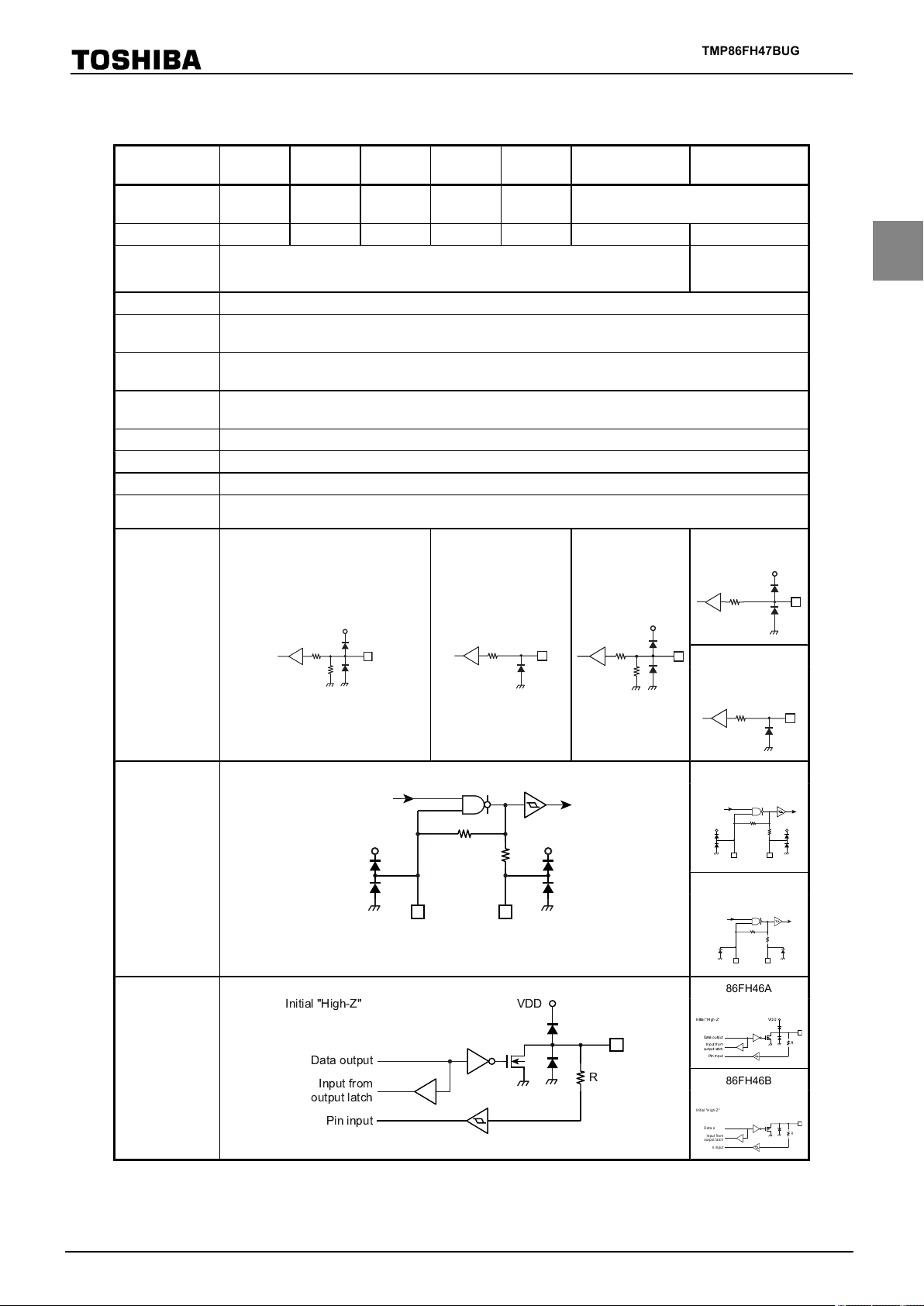
Initial "High-Z"
Input from
output latch
Data output
Pin input
R
TMP86FH47BUG
86C846
ROM
8192bytes
(MASK)
86CH46
86CH46A
16384bytes
(MASK)
86CM46
86CM46A
32768bytes
(MASK)
86PH46
16384bytes
(OTP)
86PM46
86PM46A
32768bytes
(OTP)
86FH46
16384bytes
(FLASH)
RAM 512bytes 512bytes 1024bytes 512bytes 1024bytes 512bytes 512bytes
DBR(note1) -
I/O 33pins
Large current out-
put
Interrupt
Timer counter
(External : 6 Internal : 12)
19pins
(LED direct
drive)
18interrupt sources
16-bit timer counter : 1ch
8-bit timer
counter : 2ch
UART 8-bit UART : 1ch
SIO High-Speed SIO : 1ch
Key-on wakeup 4ch
10-bit AD convert-
er
Analog-input : 8ch
86FH46A
86FH46B
128bytes (Flash con-
trol register
con-
tained)
86FH46A
Structure
pin
of TEST
Structure
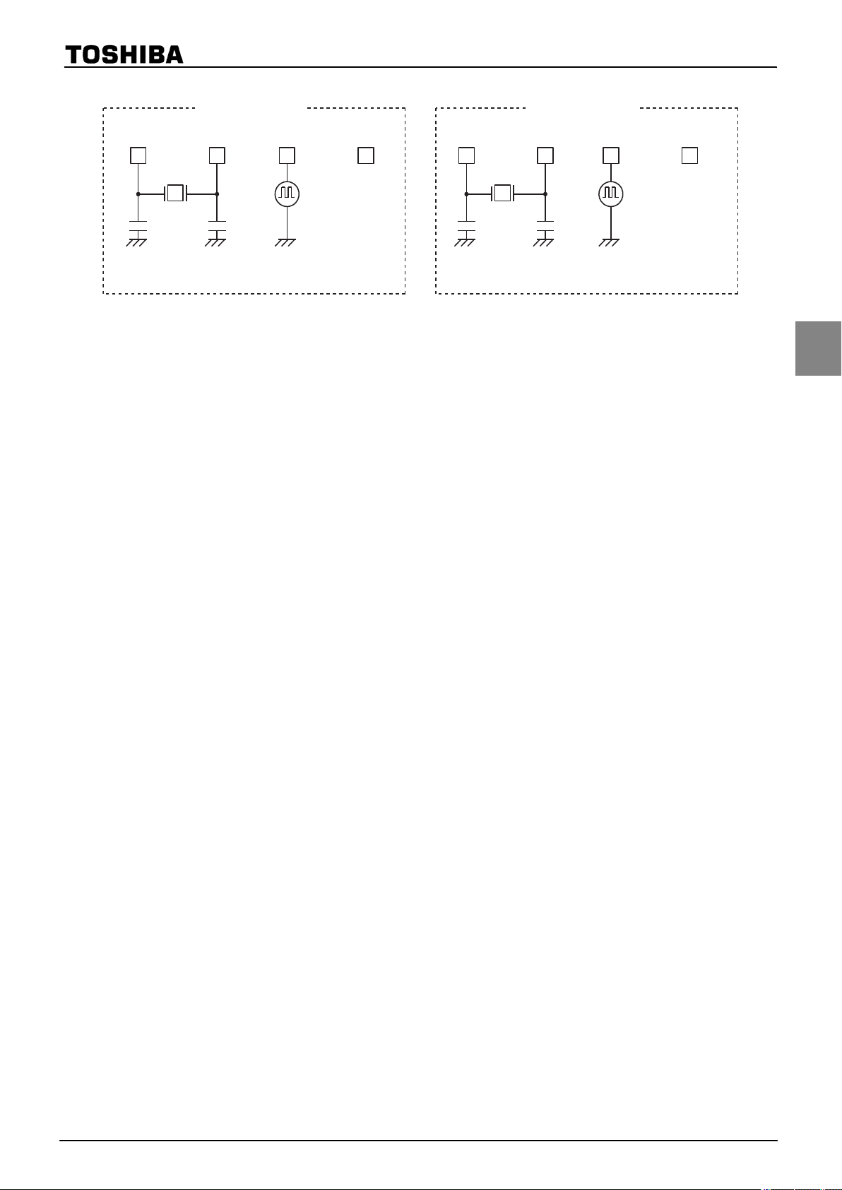
of XTIN,XTOUT
Structure
port
of P2
86FH46B
86FH46A
86FH46B
86FH46A
86FH46B
Page 4

TMP86FH47BUG
86C846
Number of guaran-
teed writes
flash memory
Terminal for SERI-
AL PROM
Flash Security N.A. Read protect
Emulation Chip TMP86C947XB
to
MODE
(note2)
Package SDIP42-P-600-1.78
86CH46
86CH46A
- - 100 Times
86CM46
86CM46A
-
86PH46
86PM46
86PM46A
86FH46
BOOT1/RXD(P10)
BOOT2/TXD(P11)
86FH46A
86FH46B
(a)86FH46A
100 Times
(b)86FH46B
Times
1000
BOOT/RXD(P02)
TXD(P03)
(a)86FH46A
Read protect
(b)86FH46B
/ Write
Read
protect
Note 1: The products with Flash memory (86FH46,86FH46A,86FH46B) contain the Flash control register (FLSCR) at 0FFFH
DBR area. The products with mask ROM or OTP and the emulation chip do not have the FLSCR register. In
in the
these devices,therefore, a program that accesses the FLSCR register cannot function properly (executes differently
as in the case of a Flash product).
Note 2: The TXD and RXD pins to be used in Serial PROM mode differ between the 86FH46 and the 86FH46A,86FH46B.
Take this into consideration in your board design when you replace the product. Details of the function refer to the chapter of the 86FH46,86FH46A,86FH46B data sheet.
Note 3: P21,P22 combine XTIN,XTOUT and port.
Page 5
Difference among product (TMP86xx47 Series)
VDD
R
IN
R
R
without pull
down resister
without protect diode
on the VDD side
VDD
R
IN
R
R
VDD
without pull
down resister
R
without pull
down resister
without protect diode
on the VDD side
fs
Rf
R
O
Osc. enable
XTIN
XTEN
XTOUT
VDDVDD
fs
Rf
R
O
Osc. enable
XTIN
XTEN
XTOUT
VDDVDD
fs
Rf
R
O
Osc. enable
XTIN
XTEN
XTOUT
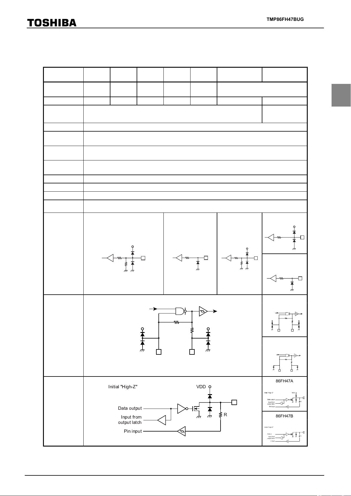
Initial "High-Z"
Input from
output latch
Data output
Pin input
R
TMP86FH47BUG
86C847
ROM
8192bytes
(MASK)
86CH47
86CH47A
16384bytes
(MASK)
86CM47
86CM47A
32768bytes
(MASK)
86PH47
16384bytes
(OTP)
86PM47
86PM47A
32768bytes
(OTP)
86FH47
16384bytes
(FLASH)
RAM 512bytes 512bytes 1024bytes 512bytes 1024bytes 512bytes 512bytes
DBR(note1) -
I/O 35pins
Large current out-
put
Interrupt
Timer counter
(External :
19pins
(LED direct
drive)
18interrupt sources
6 Internal : 12)
16-bit timer counter : 1ch
8-bit timer
counter : 2ch
UART 8-bit UART : 1ch
SIO High-Speed SIO : 1ch
Key-on wakeup 4ch
10-bit AD convert-
er
Analog-input : 8ch
86FH47A
86FH47B
128bytes (Flash con-
trol register
con-
tained)
86FH47A
Structure
pin
of TEST
Structure
of XTIN,XTOUT
Structure
port
of P2
86FH47B
86FH47A
86FH47B
86FH47A
86FH47B
Page 6

TMP86FH47BUG
86C847
Number of guaran-
teed writes
flash memory
Terminal for SERI-
AL PROM
Flash Security N.A. Read protect
Emulation Chip TMP86C947XB
(LQFP44-
P-1010-0.80A)
(LQFP44-
P-1010-0.80B)
to
MODE
(note2)
Package
Available
Package
N.A.
86CH47
86CH47A
- - 100 Times
Available
(86CH47)
Available
(86CH47A)
86CM47
86CM47A
-
Available N.A. Available Available N.A.
N.A. Available N.A. N.A. Available
86PH47
86PM47
86PM47A
86FH47
BOOT1/RXD(P10)
BOOT2/TXD(P11)
86FH47A
86FH47B
(a)86FH47A
100 Times
(b)86FH47B
1000
BOOT/RXD(P02)
TXD(P03)
(a)86FH47A
Read protect
(b)86FH47B
Read
protect
Times
/ Write
Note 1: The products with Flash memory (86FH47,86FH47A,86FH47B) contain the Flash control register (FLSCR) at 0FFFH
DBR area. The products with mask ROM or OTP and the emulation chip do not have the FLSCR register. In
in the
these devices,therefore, a program that accesses the FLSCR register cannot function properly (executes differently
as in the case of a Flash product).
Note 2: The TXD and RXD pins to be used in Serial PROM mode differ between the 86FH47 and the 86FH47A,86FH47B.
Take this into consideration in your board design when you replace the product. Details of the function refer to the chapter of the 86FH47,86FH47A,86FH47B data sheet.
Note 3: P21,P22 combine XTIN,XTOUT and port.
Page 7
Differences in Electrical Characteristics (TMP86xx46 Series)
5.5
4.5
2.7
1.8
1 4.2 8 16 [MHz]
[V]
(a)
5.5
4.5
2.7
1.8
2.0
0.030
0.034
1 4.2 8 16 [MHz]
[V]
(a)
(b)
(Note1)
5.5
4.5
2.7
1.8
1 4.2 8 16 [MHz]
[V]
(a)
5.5
4.5
3.0
2.7
1.8
0.030
0.034
1 4.2 8 16
(a)
(b)
(Note2)
[MHz]
[V]
5.5
4.5
2.7
1.8
0.030
0.034
1 4.2 8 16 [MHz]
[V]
(a)
5.5
4.5
2.7
1.8
2 4 8 16 [MHz]
[V]
(a)
5.5
4.5
2.7
1.8
0.030
0.034
2 4.2 8 16 [MHz]
[V]
(a)
TMP86FH47BUG
Operating condition
(MCU
mode)
Read/
Fetch
Erase/
Program
86C846 / 86CH46 / 86CM46
86CM46A
86PM46
86PH46
86CH46A
(a) 1.8V to 5.5V (-40 to 85 °C) (a) 2.0V to 5.5V (-40 to 85 °C)
(b) 1.8V
to 2.0V (-20 to 85 °C)
- - -
86FH46
(a) 2.7V to 5.5V (-40 to 85 °C)
86FH46A
86FH46B
TMP86FH46A
(a) 3.0V
to 5.5V (-40 to 85 °C)
(b) 2.7V to 3.0V (-20 to 85 °C)
TMP86FH46B
(a) 2.7V to 5.5V (-40 to 85 °C)
Operating condition
(Serial PROM
mode)
Supply voltage
(Absolute Maxi-
mum
Ratings)
Operating current
Note 1: With The 86CH46A,PH46 the operating temperature (Topr) is -20 °C to 85 °C when the supply voltage VDD is less
2: With The 86FH46A, the operating temperature (Topr) is -20 °C to 85 °C when the supply voltage VDD is less than
Note
Note 3: With The 86FH46A,86FH46B when a program is executing in the Flash memory or when data is being read from the
Note 4: About the measurement condition of supply current, VIN level of TEST pin is deffrent between 86FH46B and the oth-
(a) 4.5V to 5.5V (-10 to 40 °C)
- -
(a) 4.5V to 5.5V (20 to 30 °C) (a) 4.5V to 5.5V (-10 to 40 °C)
86FH46A
−0.3 ~ 6.5
(a)−0.3 ~
6.5
86FH46B
(a)−0.3 ~ 6.0
Operating current varies with each product. For details, refer to the datacheet (electrical chracteristics) of each product.(Note4)
(Note3)
than 2.0V.
3.0V.
Flash memory, the Flash memory operates in an intermittent manner causing peak currents in the Flash memory momentarily, as shown in Figure. in this case, the supply current IDD(in NORMAL1,NORMAL2 and SLOW1 mode) is defined as the sum of the average peak current and MCU current.
er 86xx46 series MCUs. The supply current is defined as follows; VIN of TEST pin: VIN ≤ 0.1V(86FH46B), VIN ≤ 0.2V(others) It is described in the section "Electrical characteristics" of TMP86FH46B in detail.
Page 8

n
Program counter (PC)
n+1 n+2 n+3
1 machine cycle(4/fc or 4/fs)
MCU current
I
[mA]
DDP-P
Typ. current
Momentary Flash current
Max. current
Sum of average momentary
Flash current and MCU curren
t
Intermittent Operation of Flash Memory
TMP86FH47BUG
Page 9

Differences in Electrical Characteristics (TMP86xx47 Series)
5.5
4.5
2.7
1.8
1 4.2 8 16 [MHz]
[V]
(a)
5.5
4.5
2.7
1.8
2.0
0.030
0.034
1 4.2 8 16 [MHz]
[V]
(a)
(b)
(Note1)
5.5
4.5
2.7
1.8
1 4.2 8 16 [MHz]
[V]
(a)
5.5
4.5
3.0
2.7
1.8
0.030
0.034
1 4.2 8 16
(a)
(b)
(Note2)
[MHz]
[V]
5.5
4.5
2.7
1.8
0.030
0.034
1 4.2 8 16 [MHz]
[V]
(a)
5.5
4.5
2.7
1.8
2 4 8 16 [MHz]
[V]
(a)
5.5
4.5
2.7
1.8
0.030
0.034
2 4.2 8 16 [MHz]
[V]
(a)
TMP86FH47BUG
Operating condition
(MCU
mode)
Read/
Fetch
Erase/
Program
86C847 / 86CH47 / 86CM47
86CM47A
86PM47
(a) 1.8V to 5.5V (-40 to 85 °C)
- - -
86PH47
86CH47A
(a) 2.0V to 5.5V (-40 to 85 °C)
(b) 1.8V
to 2.0V (-20 to 85 °C)
86FH47
(a) 2.7V to 5.5V (-40 to 85 °C)
86FH47A
86FH47B
86FH47A
(a) 3.0V
to 5.5V (-40 to 85 °C)
(b) 2.7V to 3.0V (-20 to 85 °C)
86FH47B
(a) 2.7V to 5.5V (-40 to 85 °C)
Operating condition
(Serial PROM
mode)
Supply voltage
(Absolute Maxi-
mum
Ratings)
Operating current
Note 1: With The 86CH47A, PH47 the operating temperature (Topr) is -20 °C to 85 °C when the supply voltage VDD is less
2: With The 86FH47A, the operating temperature (Topr) is -20 °C to 85 °C when the supply voltage VDD is less than
Note
Note 3: With The 86FH47A,86FH47B when a program is executing in the Flash memory or when data is being read from the
Note 4: About the measurement condition of supply current, VIN level of TEST pin is deffrent between 86FH47B and the oth-
(a) 4.5V to 5.5V (-10 to 40 °C)
- -
(a) 4.5V to 5.5V (20 to 30 °C) (a) 4.5V to 5.5V (-10 to 40 °C)
86FH47A
−0.3 ~ 6.5
(a)−0.3 ~
6.5
86FH47B
(a)−0.3 ~ 6.0
Operating current varies with each product. For details, refer to the datacheet (electrical chracteristics) of each product.(Note4)
(Note3)
than 2.0V.
3.0V.
Flash memory, the Flash memory operates in an intermittent manner causing peak currents in the Flash memory momentarily, as shown in Figure. in this case, the supply current IDD(in NORMAL1,NORMAL2 and SLOW1 mode) is defined as the sum of the average peak current and MCU current.
er 86xx47 series MCUs. The supply current is defined as follows; VIN of TEST pin: VIN ≤ 0.1V(86FH47B), VIN ≤ 0.2V(others) It is described in the section "Electrical characteristics" of TMP86FH47B in detail.
Page 10

n
Program counter (PC)
n+1 n+2 n+3
1 machine cycle(4/fc or 4/fs)
MCU current
I
[mA]
DDP-P
Typ. current
Momentary Flash current
Max. current
Sum of average momentary
Flash current and MCU curren
t
Intermittent Operation of Flash Memory
TMP86FH47BUG
Page 11

Revision History
Date
2010/7/23 Tentative 1 1st Release of Tentative
2010/10/6 1 First Release
2011/5/10 2 Contents Revised
Revision Comment
Page 12

Page 13

Table of Contents
Difference among product (TMP86xx46 Series)
TMP86FH47BUG
1.1 Features......................................................................................................................................1
1.2 Pin Assignment..........................................................................................................................3
1.3 Block Diagram...........................................................................................................................
1.4 Pin
Names
Functions..........................................................................................................5
and
4
2. Operational Description
2.1 CPU Core Functions ................................................................................................................7
2.1.1 Memory Address Map .......................................................................................................................................................7
2.1.2 Program Memory (Flash) ...................................................................................................................................................7
2.1.3 Data Memory
(RAM) .........................................................................................................................................................7
2.2 System Clock Controller ..........................................................................................................8
2.2.1 Clock Generator .................................................................................................................................................................8
2.2.2 Timing Generator .............................................................................................................................................................10
2.2.2.1 Configuration of timing generator
2.2.2.2 Machine cycle
2.2.3 Operation Mode Control Circuit ......................................................................................................................................11
2.2.3.1 Single-clock mode
2.2.3.2 Dual-clock mode
2.2.3.3 STOP mode
2.2.4 Operating Mode Control ..................................................................................................................................................16
2.2.4.1 STOP mode
2.2.4.2 IDLE1/2 mode and SLEEP1/2 mode
2.2.4.3 IDLE0 and SLEEP0 modes (IDLE0, SLEEP0)
2.2.4.4 SLOW mode
2.3 Reset Circuit ...........................................................................................................................29
2.3.1 External Reset Input .........................................................................................................................................................29
2.3.2 Address trap reset .............................................................................................................................................................30
2.3.3 Watchdog timer reset .......................................................................................................................................................30
2.3.4 System clock reset ............................................................................................................................................................30
3. Interrupt Control Circuit
3.1 Interrupt latches (IL15 to IL2)
...............................................................................................31
3.2 Interrupt enable register (EIR) ...............................................................................................32
3.2.1 Interrupt master enable flag (IMF) ..................................................................................................................................32
3.2.2 Individual interrupt enable flags (EF15 to EF4) .............................................................................................................32
3.3 Interrupt Source Selector (INTSEL).......................................................................................35
3.4 Interrupt Sequence ................................................................................................................35
3.4.1 Interrupt acceptance processing is packaged as follows. ................................................................................................35
3.4.2 Saving/restoring general-purpose registers ......................................................................................................................36
3.4.2.1 Using PUSH and POP instructions
3.4.2.2 Using data transfer instructions
3.4.3 Interrupt return .................................................................................................................................................................38
i
Page 14

3.5 Software Interrupt (INTSW) ..................................................................................................39
3.5.1 Address error
3.5.2 Debugging ........................................................................................................................................................................39
detection ....................................................................................................................................................39
3.6 Undefined Instruction Interrupt (INTUNDEF) ......................................................................39
3.7 Address Trap Interrupt (INTATRAP) ...................................................................................39
3.8 External Interrupts ..................................................................................................................39
4. Special Function Register (SFR)
4.1 SFR..........................................................................................................................................43
4.2 DBR.........................................................................................................................................45
5. Time Base Timer (
TBT)
5.1 Time Base Timer.....................................................................................................................47
5.1.1 Configuration.....................................................................................................................................................................47
5.1.2 Control...............................................................................................................................................................................47
5.1.3 Function.............................................................................................................................................................................48
5.2 Divider Output (DVO)............................................................................................................49
5.2.1 Configuration.....................................................................................................................................................................49
5.2.2 Control...............................................................................................................................................................................49
6. Watchdog Timer (WDT)
6.1 Watchdog Timer Configuration .............................................................................................51
6.2 Watchdog Timer Control .......................................................................................................52
6.2.1 Malfunction Detection Methods Using the
6.2.2 Watchdog Timer Enable ..................................................................................................................................................53
6.2.3 Watchdog Timer Disable .................................................................................................................................................54
6.2.4 Watchdog Timer Interrupt (INTWDT) ............................................................................................................................54
6.2.5 Watchdog Timer Reset .....................................................................................................................................................55
6.3 Address Trap ..........................................................................................................................56
6.3.1 Selection of Address Trap in Internal RAM (ATAS) .....................................................................................................56
6.3.2 Selection of Operation at Address Trap (ATOUT) .........................................................................................................56
6.3.3 Address Trap Interrupt (INTATRAP)...............................................................................................................................56
6.3.4 Address Trap Reset...........................................................................................................................................................57
Watchdog Timer .........................................................................................52
7. I/O Ports
7.1 Port P0 (P07 to P00)
7.2 Port P1 (P17 to P10)...............................................................................................................61
7.3 Port P2 (P22 to P20)...............................................................................................................62
7.4 Port P3 (P37 to P30)...............................................................................................................63
7.5 Port P4 (P47 to P40)...............................................................................................................65
...............................................................................................................60
8. 16-Bit Timer/Counter 1 (TC1)
8.1 Configuration...........................................................................................................................67
8.2 Timer/Counter Control............................................................................................................68
ii
Page 15

8.3 Function...................................................................................................................................70
8.3.1 Timer mode........................................................................................................................................................................70
8.3.2 External Trigger Timer
8.3.3 Event Counter Mode.........................................................................................................................................................74
8.3.4 Window Mode...................................................................................................................................................................75
8.3.5 Pulse Width Measurement Mode......................................................................................................................................76
8.3.6 Programmable Pulse Generate (PPG) Output Mode........................................................................................................79
Mode...........................................................................................................................................72
9. 8-Bit TimerCounter (TC3, TC4)
9.1 Configuration ..........................................................................................................................83
9.2 TimerCounter Control.............................................................................................................84
9.3 Function...................................................................................................................................89
9.3.1 8-Bit Timer Mode (TC3
9.3.2 8-Bit Event Counter Mode (TC3, 4).................................................................................................................................90
9.3.3 8-Bit Programmable Divider Output (PDO) Mode (TC3, 4)...........................................................................................90
9.3.4 8-Bit Pulse Width Modulation (PWM) Output Mode (TC3, 4)......................................................................................93
9.3.5 16-Bit Timer Mode (TC3 and 4)......................................................................................................................................95
9.3.6 16-Bit Event Counter Mode (TC3 and 4).........................................................................................................................96
9.3.7 16-Bit Pulse Width Modulation (PWM) Output Mode (TC3 and 4)..............................................................................96
9.3.8 16-Bit Programmable Pulse Generate (PPG) Output Mode (TC3 and 4).......................................................................99
9.3.9 Warm-Up Counter Mode.................................................................................................................................................101
9.3.9.1 Low-Frequency Warm-up Counter Mode
(NORMAL1 → NORMAL2 → SLOW2 → SLOW1)
9.3.9.2 High-Frequency Warm-Up Counter Mode
(SLOW1 → SLOW2 → NORMAL2 → NORMAL1)
and 4)........................................................................................................................................89
10. Synchronous Serial Interface (SIO)
10.1 Configuration ......................................................................................................................103
10.2 Control.................................................................................................................................104
10.3 Function...............................................................................................................................106
10.3.1 Serial clock....................................................................................................................................................................106
10.3.1.1 Clock source
10.3.1.2
10.3.2 Transfer bit direction.....................................................................................................................................................108
10.3.2.1 Transmit mode
10.3.2.2 Receive mode
10.3.2.3 Transmit/receive mode
10.3.3 Transfer modes..............................................................................................................................................................109
10.3.3.1 Transmit mode
10.3.3.2 Receive mode
10.3.3.3 Transmit/receive mode
Shift edge
11. Asynchronous Serial interface (UART)
11.1 Configuration ......................................................................................................................121
11.2 Control ................................................................................................................................ 122
11.3 Transfer Data Format
11.4 Transfer Rate.......................................................................................................................126
11.5 Data Sampling Method........................................................................................................126
11.6 STOP Bit Length................................................................................................................. 127
11.7 Parity....................................................................................................................................127
11.8 Transmit/Receive Operation................................................................................................127
11.8.1 Data Transmit Operation...............................................................................................................................................127
11.8.2 Data Receive Operation.................................................................................................................................................127
..........................................................................................................125
iii
Page 16

11.9 Status Flag........................................................................................................................... 128
11.9.1 Parity Error....................................................................................................................................................................128
11.9.2 Framing Error................................................................................................................................................................128
11.9.3 Overrun Error................................................................................................................................................................128
11.9.4 Receive Data Buffer Full..............................................................................................................................................129
11.9.5 Transmit Data Buffer Empty.........................................................................................................................................129
11.9.6 Transmit End Flag
.........................................................................................................................................................130
12. 10-bit AD Converter (ADC)
12.1 Configuration ......................................................................................................................131
12.2 Register configuration.........................................................................................................132
12.3
12.4 STOP/SLOW Modes during AD Conversion.....................................................................137
12.5 Analog Input Voltage and AD Conversion Result.............................................................138
12.6 Precautions about AD Converter........................................................................................139
Function..............................................................................................................................135
12.3.1 Software Start Mode......................................................................................................................................................135
12.3.2 Repeat Mode..................................................................................................................................................................135
12.3.3 Register Setting............................................................................................................................................................136
12.6.1 Analog input pin voltage range.....................................................................................................................................139
12.6.2 Analog input shared pins...............................................................................................................................................139
12.6.3 Noise Countermeasure...................................................................................................................................................139
13. Key-on Wakeup (KWU)
13.1 Configuration.......................................................................................................................141
13.2 Control.................................................................................................................................141
13.3 Function...............................................................................................................................141
14. Flash Memory
14.1 Flash Memory Control........................................................................................................144
14.1.1 Flash Memory Command Sequence Execution Control (FLSCR<FLSMD>)............................................................144
14.2 Command
14.2.1 Byte Program.................................................................................................................................................................145
14.2.2 Sector Erase (4-kbyte Erase).........................................................................................................................................145
14.2.3 Chip Erase (All Erase)..................................................................................................................................................146
14.2.4 Product ID Entry...........................................................................................................................................................146
14.2.5 Product ID Exit..............................................................................................................................................................146
14.2.6 Security Program...........................................................................................................................................................146
14.3 Toggle Bit (D6)...................................................................................................................147
14.4 Access to the Flash Memory Area......................................................................................148
14.4.1 Flash Memory Control in the Serial PROM Mode......................................................................................................148
14.4.1.1 How to write to the flash memory by executing the control program in the RAM area (in the RAM loader mode within the
14.4.2 Flash Memory Control in the MCU mode...................................................................................................................150
14.4.2.1 How to write to the flash memory by executing a user write control program in the RAM area (in the MCU mode)
Sequence............................................................................................................145
serial PROM mode)
15. Serial PROM Mode
15.1 Outline.................................................................................................................................153
15.2 Memory Mapping................................................................................................................153
15.3 Serial PROM Mode Setting................................................................................................154
iv
Page 17

15.3.1 Serial PROM Mode Control Pins.................................................................................................................................154
15.3.2 Pin Function...................................................................................................................................................................154
15.3.3 Example Connection for
15.3.4 Activating the Serial PROM Mode...............................................................................................................................156
On-Board Writing.................................................................................................................155
15.4 Interface Specifications for UART.....................................................................................157
15.5 Operation Command...........................................................................................................158
15.6 Operation Mode...................................................................................................................158
15.6.1 Flash Memory Erasing Mode (Operating command: F0H).........................................................................................160
15.6.2 Flash Memory Writing Mode (Operation command: 30H).........................................................................................162
15.6.3 RAM Loader Mode (Operation Command: 60H)........................................................................................................165
15.6.4 Flash Memory SUM Output Mode (Operation Command: 90H)................................................................................167
15.6.5 Product ID Code Output Mode (Operation Command: C0H).....................................................................................168
15.6.6 Flash Memory Status Output Mode (Operation Command: C3H)..............................................................................170
15.6.7 Flash Memory security program Setting Mode (Operation Command: FAH)............................................................172
15.7 Error Code...........................................................................................................................174
15.8 Checksum (SUM)................................................................................................................174
15.8.1 Calculation Method.......................................................................................................................................................174
15.8.2 Calculation data.............................................................................................................................................................175
15.9 Intel Hex Format (Binary)...................................................................................................176
15.10 Passwords..........................................................................................................................176
15.10.1 Password String...........................................................................................................................................................177
15.10.2 Handling of Password Error........................................................................................................................................177
15.10.3 Password Management during Program Development..............................................................................................177
15.11 Product ID Code................................................................................................................178
15.12 Flash Memory Status Code...............................................................................................178
15.13 Specifying the Erasure Area..............................................................................................180
15.14 Port Input Control Register...............................................................................................180
15.15 Flowchart...........................................................................................................................182
15.16 UART Timing...................................................................................................................183
16. Input/Output Circuitry
16.1 Control Pins.........................................................................................................................185
16.2 Input/Output Ports...............................................................................................................186
17. Electrical Characteristics
17.1 Absolute Maximum Ratings................................................................................................187
17.2 Operating Conditions...........................................................................................................188
17.2.1 Serial
17.2.2 MCU mode (Except Flash Programming or erasing) .................................................................................................188
17.2.3 MCU mode (Flash Programming or erasing) ..............................................................................................................189
PROM mode.......................................................................................................................................................188
17.3 DC Characteristics ..............................................................................................................190
17.4 AD Characteristics...............................................................................................................192
17.5 AC Characteristics...............................................................................................................193
17.6 Flash Characteristics............................................................................................................194
17.6.1 Write Characteristics.....................................................................................................................................................194
17.7 Oscillating Conditions.........................................................................................................195
17.8 Handling Precaution............................................................................................................195
18. Package Dimensions
v
Page 18

vi
Page 19

CMOS 8-Bit Microcontroller
TMP86FH47BUG
TMP86FH47BUG
The TMP86FH47BUG
is a single-chip 8-bit high-speed and high-functionality microcomputer incorporating
16384 bytes of Flash Memory. It is pin-compatible with the TMP86CH47AUG/TMP86C847UG (Mask ROM version). The TMP86FH47BUG can realize operations equivalent to those of the TMP86CH47AUG/TMP86C847UG
by programming the on-chip Flash Memory.
Product No.
TMP86FH47BUG
ROM
(FLASH)
16384
bytes
RAM Package MASK ROM MCU Emulation Chip
512
bytes
P-LQFP44-1010-0.80B
TMP86CH47AUG/
TMP86C847UG
TMP86C947XB
1.1 Features
1. 8-bit single
- Instruction execution time :
- 132 types & 731 basic instructions
2. 18interrupt sources (External : 6 Internal : 12)
chip microcomputer TLCS-870/C series
0.25 μs (at 16 MHz)
122 μs (at 32.768 kHz)
3. Input / Output ports (35 pins)
Large current output: 19pins (Typ. 20mA), LED direct drive
4. Prescaler
- Time base timer
- Divider output function
5. Watchdog Timer
6. 16-bit timer counter: 1 ch
- Timer, External trigger, Window, Pulse width measurement,
Event counter, Programmable pulse generate (PPG) modes
7. 8-bit timer counter : 2 ch
- Timer, Event counter, Programmable divider output (PDO),
Pulse width modulation (PWM) output,
Programmable pulse generation (PPG),
16bit mode (8bit timer 2ch combination) modes
8. Serial Interface
- High-Speed 8-bit SIO: 1ch
9. 8-bit UART : 1 ch
This product uses the Super Flash® technology under the licence of Silicon Storage Technology, Inc. Super Flash® is registered trademark of Silicon Storage
Technology, Inc.
Page 1
RA000
Page 20

1.1 Features
TMP86FH47BUG
10. 10-bit successive approximation type AD converter
- Analog input:
8 ch
11. Key-on wakeup : 4 ch
12. Clock operation
Single clock mode
Dual clock mode
13. Low power consumption operation
STOP mode: Oscillation stops. (Battery/Capacitor back-up.)
SLOW1 mode: Low power consumption operation using low-frequency clock.(High-frequency clock
stop.)
SLOW2 mode: Low power consumption operation using low-frequency clock.(High-frequency clock os-
cillate.)
IDLE0 mode: CPU stops, and only the Time-Based-Timer(TBT) on peripherals operate using high fre-
quency clock. Release by falling edge of the source clock which is set by TBTCR<TBTCK>.
IDLE1 mode: CPU stops and peripherals operate using high frequency clock. Release by interruputs
(CPU restarts).
IDLE2 mode: CPU stops and peripherals operate using high and low frequency clock. Release by inter-
ruputs. (CPU restarts).
SLEEP0 mode: CPU stops, and only the Time-Based-Timer(TBT) on peripherals operate using low fre-
quency clock.Release by falling edge of the source clock which is set by TBTCR<TBTCK>.
SLEEP1 mode: CPU stops, and peripherals operate using low frequency clock. Release by interruput.
(CPU restarts).
SLEEP2 mode: CPU stops and peripherals operate using high and low frequency clock. Release by inter-
ruput.
14. Wide operation voltage:
4.5 V to 5.5 V at 16MHz /32.768 kHz
2.7 V to 5.5 V at 8 MHz /32.768 kHz
RA000
Page 2
Page 21
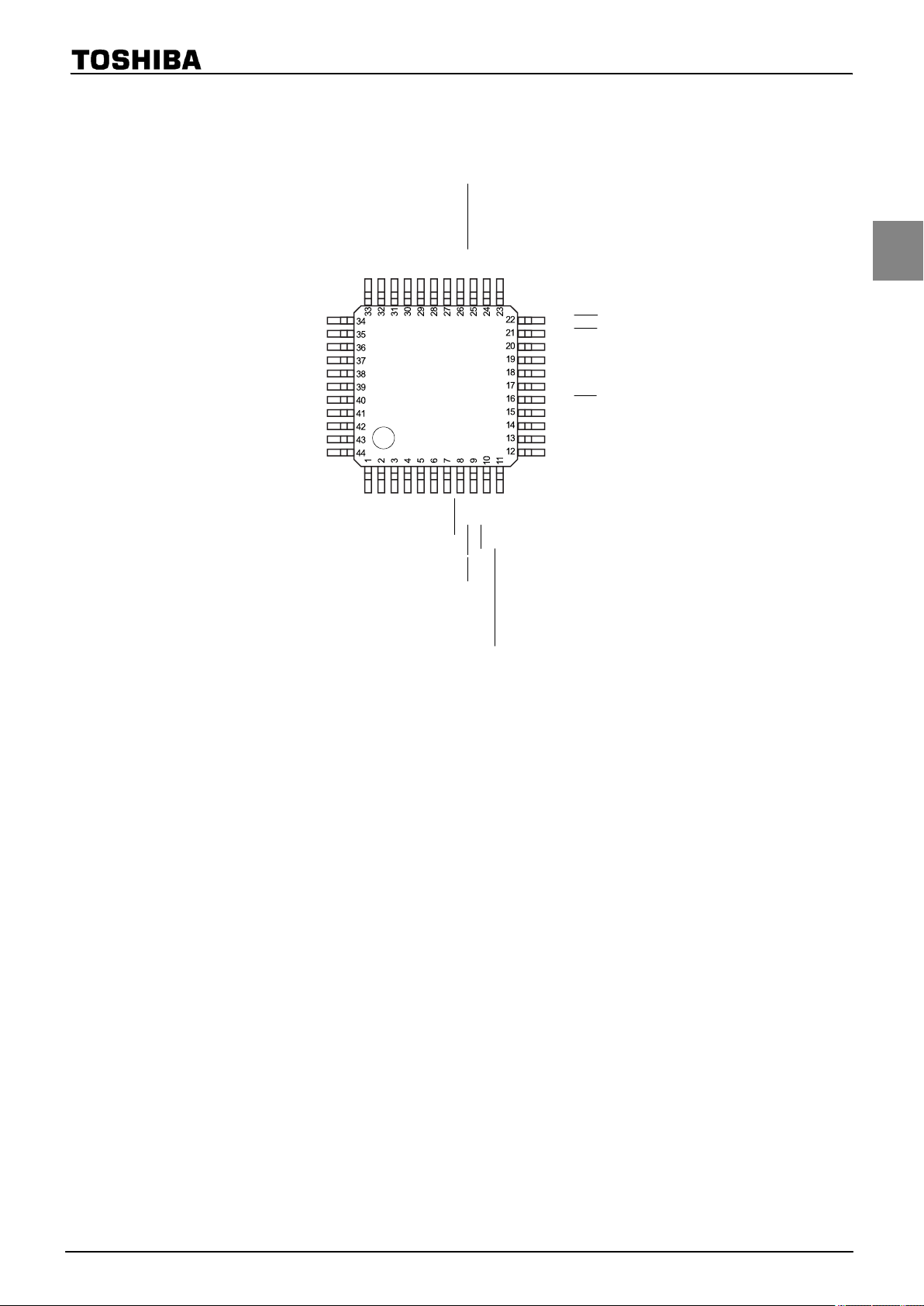
1.2 Pin Assignment
PDO3/PWM3/TC3)
P37 (AIN7/STOP5)
P36 (AIN6/STOP4)
P35 (AIN5/STOP3)
P34 (AIN4/STOP2)
P33 (AIN3)
P32 (AIN2)
P31 (AIN1)
P30 (AIN0)
P10 (
P11 (INT1)
P12 (INT2/TC1)
VAREF P13 (DVO)
AVDD P14 (PPG)
AVSS P15 (INT3)
P40 P16
P41 P17
P42 P07 (INT4)
P43 P06 (
P44 P05 (SI)
P45 P04 (SO)
P46 P03 (TXD)
P47 P02 (RXD/BOOT)
SCK)
TMP86FH47BUG
XIN
VSS
TEST
XOUT
VDD
(XTIN) P21
(XTOUT) P22
RESET
INT5/STOP) P20
(
INT0) P00
(
(PDO4/PWM4/PPG4/TC4) P01
Figure 1-1 Pin Assignment
RA000
Page 3
Page 22
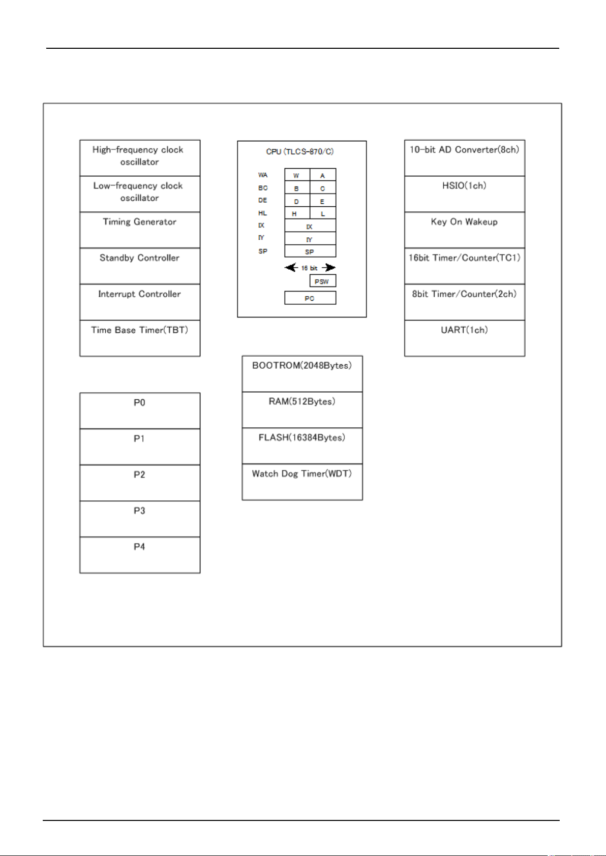
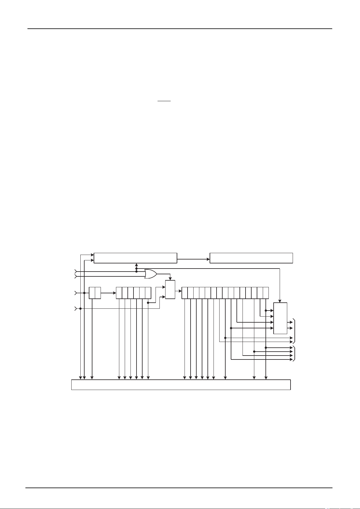
1.3 Block Diagram
1.3 Block Diagram
TMP86FH47BUG
RA000
Figure 1-2 Block Diagram
Page 4
Page 23
1.4 Pin Names and Functions
TMP86FH47BUG
The TMP86FH47BUG
has MCU mode, parallel PROM mode, and serial PROM mode. Table 1-1 shows the
pin functions in MCU mode. The serial PROM mode is explained later in a separate chapter.
Table 1-1 Pin Names and Functions(1/3)
Pin Name
P07
INT4
P06
SCK
P05
SI
P04
SO
P03
TXD
P02
RXD
BOOT
P01
TC4
PDO4/PWM4/PPG4
Pin Number Input/Output Functions
17
16
15
14
13
12
11
IOIPORT07
External interrupt
IOIOPORT06
Serial clock
IOIPORT05
Serial data
IOOPORT04
Serial data
IOOPORT03
UART data
IO
PORT02
I
UART data
I
Serial PROM mode control input
IO
PORT01
I
TC4 input
O
PDO4/PWM4/PPG4
input/output
input
output
output
input
4 input
output
P00
INT0
P17 18 IO PORT17
P16 19 IO PORT16
P15
INT3
P14
PPG
P13
DVO
P12
INT2
TC1
P11
INT1
P10
PDO3/PWM3
TC3
P22
XTOUT
10
20
21
22
23
24
25
7
IOIPORT00
External interrupt
IOIPORT15
External interrupt
IOOPORT14
PPG output
IOOPORT13
Divider Output
IO
PORT12
I
External interrupt
TC1 input
I
IOIPORT11
External interrupt
IO
PORT10
O
PDO3/PWM3 output
I
IO
O
input
TC3
PORT22
Resonator connecting
nal clock
0 input
3 input
2 input
1 input
pins(32.768kHz) for inputting exter-
RA000
P21
XTIN
PORT21
6
IO
Resonator connecting
I
nal clock
pins(32.768kHz) for inputting exter-
Page 5
Page 24

1.4 Pin Names and Functions
Table 1-1 Pin Names and Functions(2/3)
TMP86FH47BUG
P20
STOP
INT5
P37
AIN7
STOP5
P36
AIN6
STOP4
P35
AIN5
STOP3
P34
AIN4
STOP2
P33
AIN3
P32
AIN2
P31
AIN1
Pin Name
Pin Number Input/Output Functions
IO
PORT20
9
33
32
31
30
29
28
27
I
STOP mode
External interrupt 5 input
I
IO
PORT37
I
Analog Input7
I
STOP5
IO
PORT36
I
Analog Input6
I
STOP4
IO
PORT35
I
Analog Input5
I
STOP3
IO
PORT34
I
Analog Input4
I
STOP2
IOIPORT33
Analog Input3
IOIPORT32
Analog Input2
IOIPORT31
Analog Input1
release signal input
input
input
input
input
P30
AIN0
P47 44 IO PORT47
P46 43 IO PORT46
P45 42 IO PORT45
P44 41 IO PORT44
P43 40 IO PORT43
P42 39 IO PORT42
P41 38 IO PORT41
P40 37 IO PORT40
XIN 2 I Resonator connecting pins for high-frequency clock
XOUT 3 O Resonator connecting pins for high-frequency clock
RESET 8 IO Reset signal
TEST 4 I Test pin for out-going test. Normally, be fixed to low.
VAREF 34 I Analog Base Voltage Input Pin for A/D Conversion
26
IOIPORT30
Analog Input0
Table 1-1 Pin Names and Functions(3/3)
Pin Name Pin Number Input/Output Functions
AVDD 35 I Analog Power Supply
AVSS 36 I Analog Power Supply
VDD 5 I +5V
VSS 1 I 0(GND)
Page 6
RA000
Page 25
2. Operational Description
TMP86FH47BUG
2.1 CPU
Core Functions
The CPU core consists of a CPU, a system clock controller, and an interrupt controller.
This section provides a description of the CPU core, the program memory, the data memory, and the reset circuit.
2.1.1 Memory Address Map
The TMP86FH47BUG memory is composed Flash, RAM, DBR(Data buffer register) and SFR(Special function register). They are all mapped in 64-Kbyte address space. Figure 2-1 shows the TMP86FH47BUG memory address map.
SFR
RAM
DBR
0FFF
C000
Flash
FFC0
FFDF
FFE0
FFFF
0000
H
003F
H
0040
H
023F
H
0F80
H
H
H
H
H
H
H
64 bytes
512
bytes
128
bytes
16384
bytes
SFR:
Vector table for vector call instructions
(32 bytes)
Vector table for interrupts
(32 bytes)
Special function register includes:
I/O ports
Peripheral
Peripheral status registers
System control registers
Program status word
RAM:
Random access memory includes:
Data memory
Stack
DBR: Data buffer register includes:
Peripheral control
Peripheral status registers
Flash: Program memory
control registers
registers
Figure 2-1 Memory Address Map
2.1.2 Program
The TMP86FH47BUG has a 16384 bytes (Address C000H to FFFFH) of program memory (Flash).
Memory (Flash)
2.1.3 Data Memory (RAM)
The TMP86FH47BUG has 512bytes (Address 0040H to 023FH) of internal RAM. The first 192 bytes
(0040H to 00FFH) of the internal RAM are located in the direct area; instructions with shorten operations
are available against such an area.
Page 7
Page 26
2. Operational Description
2.2 System Clock Controller
The data memory contents become unstable when the power supply is turned on; therefore, the data memory should be initialized by an initialization routine.
Example :Clears RAM to “00H”. (TMP86FH47BUG)
SRAMCLR: LD (HL), A
2.2 System Clock Controller
TMP86FH47BUG
LD HL, 0040H ; Start address setup
LD A, H ; Initial value (00H) setup
LD BC, 01FFH
INC HL
DEC BC
JRS F, SRAMCLR
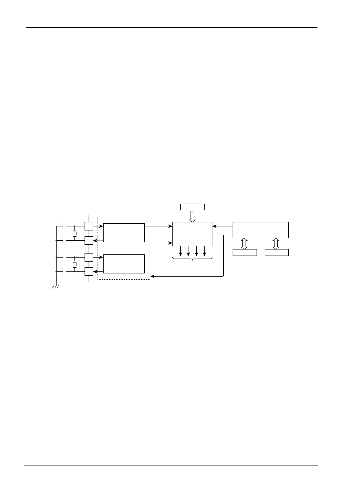
The system clock controller consists of a clock generator, a timing generator, and a standby controller.
Timing generator control register
TBTCR
0036
H
Timing
generator
System clocks
Standby controller
0038
H
0039
System control registers
XIN
XOUT
XTIN
XTOUT
Clock
generator
fc
High-frequency
clock oscillator
fs
Low-frequency
clock oscillator
Clock generator control
Figure 2-2 System Clock Control
2.2.1 Clock Generator
The clock generator generates the basic clock which provides the system clocks supplied to the CPU core
and peripheral hardware. It contains two oscillation circuits: One for the high-frequency clock and one for
the low-frequency clock. Power consumption can be reduced by switching of the standby controller to low-power operation based on the low-frequency clock.
H
SYSCR2SYSCR1
The high-frequency (fc) clock and low-frequency (fs) clock can easily be obtained by connecting a resonator between the XIN/XOUT and XTIN/XTOUT pins respectively. Clock input from an external oscillator is also possible. In this case, external clock is applied to XIN/XTIN pin with XOUT/XTOUT pin not connected.
Page 8
Page 27
TMP86FH47BUG
(a) Crystal/Ceramic
resonator
Note:The function to monitor the basic clock directly at external is not provided for hardware, however,
High-frequency clock
XOUTXIN
(b) External oscillator
XOUTXIN
(Open)
XTIN
(c) Crystal (d) External oscillator
Low-frequency clock
XTOUT
XTIN
XTOUT
(Open)
Figure 2-3 Examples of Resonator Connection
with disabling all interrupts and watchdog timers, the oscillation frequency can be adjusted by monitoring the pulse which the fixed frequency is outputted to the port by the program.
The system to require the adjustment of the oscillation frequency should create the program for the adjustment in advance.
Page 9
Page 28
2. Operational Description
2.2 System Clock Controller
2.2.2 Timing Generator
The timing generator generates the various system clocks supplied to the CPU core and peripheral hardware from the basic clock (fc or fs). The timing generator provides the following functions.
TMP86FH47BUG
1. Generation of main system clock
2. Generation of divider output (DVO) pulses
3. Generation of source clocks for time base timer
4. Generation of source clocks for watchdog timer
5. Generation of internal source clocks for timer/counters
6. Generation of warm-up clocks for releasing STOP mode
2.2.2.1 Configuration of timing generator
The timing generator consists of a 2-stage prescaler, a 21-stage divider, a main system clock generator,
and machine cycle counters.
An input clock to the 7th stage of the divider depends on the operating mode, SYSCR2<SYSCK> and
TBTCR<DV7CK>, that is shown in Figure 2-4. As reset and STOP mode started/canceled, the prescaler
and the divider are cleared to “0”.
SYSCK
DV7CK
High-frequency
clock fc
Low-frequency
clock fs
fc/4
1 21 432 87 109 1211 1413 1615
5 6 17 18 19 20 21
S
A
Y
B
Multi-
plexer
fc or fs
Machine cycle countersMain system clock generator
Divider
B0
B1
A0
A1
S
Y0
Y1
Multiplexer
Warm-up
controller
Watchdog
timer
Timer counter, Serial interface, Time-base-timer, divider output, etc. (Peripheral functions)
Figure 2-4 Configuration of Timing Generator
Page 10
Page 29
Timing Generator Control Register
TMP86FH47BUG
TBTCR
(0036H)
Note 1: In single clock mode, do not set DV7CK to “1”.
Note 2: Do not set “1” on DV7CK while the low-frequency clock is not operated stably.
Note 3: fc: High-frequency clock [Hz], fs: Low-frequency clock [Hz], *: Don’t care
Note 4: In SLOW1/2 and SLEEP1/2 modes, the DV7CK setting is ineffective, and fs is input to the 7th stage of the divider.
Note 5: When STOP mode is entered from NORMAL1/2 mode, the DV7CK setting is ineffective during the warm-up period af-
7
(DVOEN)
DV7CK
ter release of STOP mode, and the 6th stage of the divider is input to the 7th stage during this period.
6 5 4 3 2 1 0
(DVOCK) DV7CK (TBTEN) (TBTCK) (Initial value: 0000 0000)
Selection of input to the 7th stage
of the divider
0: fc/28 [Hz]
1: fs
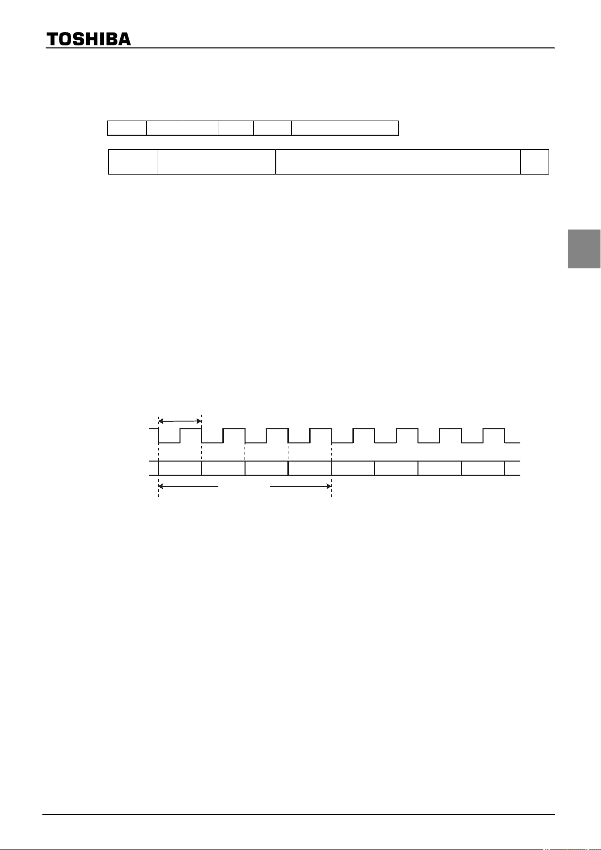
2.2.2.2 Machine cycle
Instruction execution and peripheral hardware operation are synchronized with the main system clock.
The minimum instruction execution unit is called an “machine cycle”. There are a total of 10 different
types of instructions for the TLCS-870/C Series: Ranging from 1-cycle instructions which require one machine cycle for execution to 10-cycle instructions which require 10 machine cycles for execution. A machine cycle consists of 4 states (S0 to S3), and each state consists of one main system clock.
R/W
1/fc or 1/fs [s]
Main system clock
State
Machine cycle
Figure 2-5 Machine Cycle
2.2.3 Operation Mode Control Circuit
The operation mode control circuit starts and stops the oscillation circuits for the high-frequency and low-frequency clocks, and switches the main system clock. There are three operating modes: Single clock mode, dual clock mode and STOP mode. These modes are controlled by the system control registers (SYSCR1 and
SYSCR2). Figure 2-6 shows the operating mode transition diagram.
2.2.3.1 Single-clock mode
Only the oscillation circuit for the high-frequency clock is used, and P21 (XTIN) and P22 (XTOUT)
pins are used as input/output ports. The main-system clock is obtained from the high-frequency clock. In
the single-clock mode, the machine cycle time is 4/fc [s].
S3S2S1S0 S3S2S1S0
(1) NORMAL1 mode
In this mode, both the CPU core and on-chip peripherals operate using the high-frequency clock.
The TMP86FH47BUG is placed in this mode after reset.
Page 11
Page 30

2. Operational Description
2.2 System Clock Controller
TMP86FH47BUG
(2) IDLE1 mode
In this mode, the internal oscillation circuit remains active. The CPU and the watchdog timer are hal-
ted; however
on-chip peripherals remain active (Operate using the high-frequency clock).
IDLE1 mode is started by SYSCR2<IDLE> = "1", and IDLE1 mode is released to NORMAL1
mode by an interrupt request from the on-chip peripherals or external interrupt inputs. When the
IMF (Interrupt master enable flag) is “1” (Interrupt enable), the execution will resume with the acceptance of the interrupt, and the operation will return to normal after the interrupt service is completed.
When the IMF is “0” (Interrupt disable), the execution will resume with the instruction which follows the IDLE1 mode start instruction.
(3) IDLE0 mode
In this mode, all the circuit, except oscillator and the timer-base-timer, stops operation.
This mode is enabled by SYSCR2<TGHALT> = "1".
When IDLE0 mode starts, the CPU stops and the timing generator stops feeding the clock to the peripheral circuits other than TBT. Then, upon detecting the falling edge of the source clock selected
with TBTCR<TBTCK>, the timing generator starts feeding the clock to all peripheral circuits.
When returned from IDLE0 mode, the CPU restarts operating, entering NORMAL1 mode back
again. IDLE0 mode is entered and returned regardless of how TBTCR<TBTEN> is set. When IMF
= “1”, EF6 (TBT interrupt individual enable flag) = “1”, and TBTCR<TBTEN> = “1”, interrupt processing is performed. When IDLE0 mode is entered while TBTCR<TBTEN> = “1”, the INTTBT interrupt latch is set after returning to NORMAL1 mode.
2.2.3.2 Dual-clock mode
Both the high-frequency and low-frequency oscillation circuits are used in this mode. P21 (XTIN) and
P22 (XTOUT) pins cannot be used as input/output ports. The main system clock is obtained from the highfrequency clock in NORMAL2 and IDLE2 modes, and is obtained from the low-frequency clock in
SLOW and SLEEP modes. The machine cycle time is 4/fc [s] in the NORMAL2 and IDLE2 modes, and
4/fs [s] (122 μs at fs = 32.768 kHz) in the SLOW and SLEEP modes.
The TLCS-870/C is placed in the single-clock mode during reset. To use the dual-clock mode, the lowfrequency oscillator should be turned on at the start of a program.
(1) NORMAL2 mode
In this mode, the CPU core operates with the high-frequency clock. On-chip peripherals operate us-
ing the high-frequency clock and/or low-frequency clock.
(2) SLOW2 mode
In this mode, the CPU core operates with the low-frequency clock, while both the high-frequency
clock and the low-frequency clock are operated. As the SYSCR2<SYSCK> becomes "1", the hardware changes into SLOW2 mode. As the SYSCR2<SYSCK> becomes “0”, the hardware changes into NORMAL2 mode. As the SYSCR2<XEN> becomes “0”, the hardware changes into SLOW1
mode. Do not clear SYSCR2<XTEN> to “0” during SLOW2 mode.
(3) SLOW1 mode
This mode can be used to reduce power-consumption by turning off oscillation of the high-frequency clock. The CPU core and on-chip peripherals operate using the low-frequency clock.
Page 12
Page 31

TMP86FH47BUG
Switching back and forth between SLOW1 and SLOW2 modes are performed by
SYSCR2<XEN>. In SLOW1 and SLEEP modes, the input clock to the 1st stage of the divider is stopped; output
from the 1st to 6th stages is also stopped.
(4) IDLE2 mode
In this mode, the internal oscillation circuit remain active. The CPU and the watchdog timer are halted; however, on-chip peripherals remain active (Operate using the high-frequency clock and/or the
low-frequency clock). Starting and releasing of IDLE2 mode are the same as for IDLE1 mode, except that operation returns to NORMAL2 mode.
(5) SLEEP1 mode
In this mode, the internal oscillation circuit of the low-frequency clock remains active. The CPU,
the watchdog timer, and the internal oscillation circuit of the high-frequency clock are halted; however, on-chip peripherals remain active (Operate using the low-frequency clock). Starting and releasing of SLEEP mode are the same as for IDLE1 mode, except that operation returns to SLOW1
mode. In SLOW1 and SLEEP1 modes, the input clock to the 1st stage of the divider is stopped; output from the 1st to 6th stages is also stopped.
(6) SLEEP2 mode
The SLEEP2 mode is the idle mode corresponding to the SLOW2 mode. The status under the
SLEEP2 mode is same as that under the SLEEP1 mode, except for the oscillation circuit of the highfrequency clock.
(7) SLEEP0 mode
In this mode, all the circuit, except oscillator and the timer-base-timer, stops operation. This
mode is enabled by setting “1” on bit SYSCR2<TGHALT>.
When SLEEP0 mode starts, the CPU stops and the timing generator stops feeding the clock to
the peripheral circuits other than TBT. Then, upon detecting the falling edge of the source clock selected with TBTCR<TBTCK>, the timing generator starts feeding the clock to all peripheral circuits.
When returned from SLEEP0 mode, the CPU restarts operating, entering SLOW1 mode back
again. SLEEP0 mode is entered and returned regardless of how TBTCR<TBTEN> is set. When
IMF = “1”, EF6 (TBT interrupt individual enable flag) = “1”, and TBTCR<TBTEN> = “1”, interrupt processing is performed. When SLEEP0 mode is entered while TBTCR<TBTEN> = “1”, the
INTTBT interrupt latch is set after returning to SLOW1 mode.
2.2.3.3 STOP mode
In this mode, the internal oscillation circuit is turned off, causing all system operations to be halted.
The internal status immediately prior to the halt is held with a lowest power consumption during STOP
mode.
STOP mode is started by the system control register 1 (SYSCR1), and STOP mode is released by a inputting (Either level-sensitive or edge-sensitive can be programmable selected) to the
warm-up period
is completed, the execution resumes with the instruction which follows the STOP mode
STOP pin. After the
start instruction.
Page 13
Page 32

2. Operational Description
2.2 System Clock Controller
TMP86FH47BUG
IDLE1
mode
(a) Single-clock mode
IDLE2
mode
SLEEP2
mode
SLEEP1
mode
(b) Dual-clock mode
SYSCR2<TGHALT> = "1"
SYSCR2<IDLE> = "1"
Interrupt
SYSCR2<XTEN> = "0"
SYSCR2<IDLE> = "1"
Interrupt
SYSCR2<SYSCK> = "0"
SYSCR2<IDLE> = "1"
Interrupt
SYSCR2<XEN> = "1"
SYSCR2<IDLE> = "1"
Interrupt
Note 2
IDLE0
mode
NORMAL1
mode
NORMAL2
mode
SLOW2
mode
SLOW1
mode
Reset release
Note 2
SYSCR1<STOP> = "1"
STOP pin input
SYSCR2<XTEN> = "1"
SYSCR1<STOP> = "1"
STOP pin input
SYSCR2<SYSCK> = "1"
SYSCR2<XEN> = "0"
SYSCR1<STOP> = "1"
STOP pin input
SYSCR2<TGHALT> = "1"
RESET
STOP
SLEEP0
mode
Note 1: NORMAL1 and NORMAL2 modes are generically called NORMAL; SLOW1 and SLOW2 are called SLOW;
IDLE0, IDLE1 and IDLE2 are called IDLE; SLEEP0, SLEEP1 and SLEEP2 are called SLEEP.
Note 2: The mode is released by falling edge of TBTCR<TBTCK> setting.
Figure 2-6 Operating Mode Transition Diagram
Table 2-1 Operating Mode and Conditions
Operating Mode
Single clock
Dual clock
Oscillator
High
Frequency
RESET
NORMAL1 Operate Operate
IDLE1
STOP Stop Halt -
NORMAL2
IDLE2 Halt Halt
SLOW2
SLEEP2 Halt Halt
SLOW1
SLEEP1
STOP Stop Halt Halt -
Oscillation
Oscillation
Stop
Low
Frequency
Stop
Oscillation
CPU Core WDT TBT
Reset Reset Reset Reset Reset
Operate
Halt HaltIDLE0
Operate with
High-freq.
Operate with
Low-freq.
Operate with
Low-freq.
Halt HaltSLEEP0
Operate with
High or Low-
freq.
Operate with
Low-freq.
Operate with
Low-freq.
Operate
AD
Converter
Operate Operate
Halt Halt
Operate
Halt 4/fs [s]
Peripherals
Other
Operate
Halt
Machine Cy-
cle Time
4/fc [s]
4/fc [s]
Page 14
Page 33

System Control Register 1
TMP86FH47BUG
SYSCR1
(0038H) STOP RELM RETM OUTEN WUT (Initial value: 0000 000*)
7 6 5 4 3 2 1
STOP STOP mode start
RELM
RETM
OUTEN Port output during STOP mode
WUT
Release method for STOP
mode
Operating mode after STOP
mode
Warm-up time at releasing
STOP mode
0: CPU core and peripherals remain active
core and peripherals are halted (Start STOP mode)
1: CPU
0: Edge-sensitive release
1: Level-sensitive
0: Return to NORMAL1/2 mode
1: Return
0: High impedance
1: Output
Return to NORMAL mode Return to SLOW mode
000
010
100
110
*01
*11
release
to SLOW1 mode
kept
3 x 216/fc
216/fc
3 x
214/fc
3 x 210/fc
210/fc
214/fc
0
3 x 213/fs
213/fs
3 x
26/fs
26/fs
3 x 26/fs
26/fs
Note 1: Always set RETM to “0” when transiting from NORMAL mode to STOP mode. Always set RETM to “1” when transit-
ing from
Note 2: When STOP mode is released with
Note 3: fc:
SLOW mode to STOP mode.
RESET pin input, a return is made to NORMAL1 regardless of the RETM contents.
High-frequency clock [Hz], fs: Low-frequency clock [Hz], *; Don’t care
Note 4: Bits 1 in SYSCR1 are read as undefined data when a read instruction is executed.
Note 5: As the hardware becomes STOP mode under OUTEN = “0”, input value is fixed to “0”; therefore it may cause exter-
nal interrupt request on account of falling edge.
Note 6: When the key-on wakeup is used, RELM should be set to "1".
Note 7: Port P20 is used as
comes High-Z
STOP pin. Therefore, when stop mode is started, OUTEN does not affect to P20, and P20 be-
mode.
Note 8: The warming-up time should be set correctly for using oscillator.
R/W
R/W
R/W
R/W
R/W
System Control Register 2
SYSCR2
(0039H)
7
XEN XTEN SYSCK IDLE TGHALT (Initial value: 1000 *0**)
XEN High-frequency oscillator control
XTEN Low-frequency oscillator control
SYSCK
IDLE
TGHALT
Note 1: A reset is applied if both XEN and XTEN are cleared to “0”, XEN is cleared to “0” when SYSCK = “0”, or XTEN is
cleared to
Note 2: *: Don’t care, TG: Timing generator, *; Don’t care
Note 3: Bits 3, 1 and 0 in SYSCR2 are always read as undefined value.
Note 4: Do not set IDLE and TGHALT to “1” simultaneously.
Note 5: Because returning from IDLE0/SLEEP0 to NORMAL1/SLOW1 is executed by the asynchronous internal clock, the pe-
riod of IDLE0/SLEEP0 mode might be shorter than the period setting by TBTCR<TBTCK>.
6 5 4
Main system clock select (Write)/
main system
(Read)
CPU and watchdog timer control (IDLE1/2
modes)
TG control (IDLE0 and SLEEP0
modes)
clock monitor
and SLEEP1/2
“0” when SYSCK = “1”.
3
0: Turn off oscillation
1: Turn
0: Turn off oscillation
1: Turn
0: High-frequency clock (NORMAL1/NORMAL2/IDLE1/IDLE2)
1: Low-frequency
0: CPU and watchdog timer remain active
1: CPU
modes)
0: Feeding clock to all peripherals from TG
1: Stop
(Start IDLE0 and SLEEP0 modes)
2
on oscillation
on oscillation
and watchdog timer are stopped (Start IDLE1/2 and SLEEP1/2
feeding clock to peripherals except TBT from TG
1 0
clock (SLOW1/SLOW2/SLEEP1/SLEEP2)
R/W
R/W
Page 15
Page 34

2. Operational Description
2.2 System Clock Controller
Note 6: When IDLE1/2 or SLEEP1/2 mode is released, IDLE is automatically cleared to “0”.
Note 7: When
Note 8: Before setting TGHALT to “1”, be sure to stop peripherals. If peripherals are not stopped, the interrupt latch of periph-
2.2.4 Operating Mode Control
2.2.4.1 STOP mode
TMP86FH47BUG
IDLE0 or SLEEP0 mode is released, TGHALT is automatically cleared to “0”.
erals may be set after IDLE0 or SLEEP0 mode is released.
STOP mode is controlled by the system control register 1, the
put (STOP5
The
to STOP2) which is controlled by the STOP mode release control register (STOPCR).
STOP pin is also used both as a port P20 and an INT5 (external interrupt input 5) pin. STOP
STOP pin input and key-on wakeup in-
mode is started by setting SYSCR1<STOP> to “1”. During STOP mode, the following status is maintained.
1. Oscillations are
turned off, and all internal operations are halted.
2. The data memory, registers, the program status word and port output latches are all held in the
status in effect before STOP mode was entered.
3. The prescaler and the divider of the timing generator are cleared to “0”.
4. The program counter holds the address 2 ahead of the instruction (e.g., [SET (SYSCR1).7])
which started STOP mode.
STOP mode includes a level-sensitive mode and an edge-sensitive mode, either of which can be selected with the SYSCR1<RELM>. Do not use any key-on wakeup input (STOP5 to STOP2) for releasing
STOP mode in edge-sensitive mode.
Note 1: The STOP mode can be released by either the STOP or key-on wakeup pin (STOP5 to STOP2). How-
Note 2: During STOP period (from start of STOP mode to end of warm up), due to changes in the external in-
ever, because the STOP pin is different from the key-on wakeup and can not inhibit the release input, the STOP pin must be used for releasing STOP mode.
terrupt pin signal, interrupt latches may be set to “1” and interrupts may be accepted immediately after STOP mode is released. Before starting STOP mode, therefore, disable interrupts. Also, before enabling interrupts after STOP mode is released, clear unnecessary interrupt latches.
(1) Level-sensitive release mode (RELM = “1”)
In this mode, STOP mode is released by setting the
STOP2 pin
input which is enabled by STOPCR. This mode is used for capacitor backup when the
STOP pin high or setting the STOP5 to
main power supply is cut off and long term battery backup.
Even if an instruction for starting STOP mode is executed while
STOP pin input is high or
STOP5 to STOP2 input is low, STOP mode does not start but instead the warm-up sequence starts immediately. Thus,
gram to first confirm that the
ing two
methods can be used for confirmation.
to start STOP mode in the level-sensitive release mode, it is necessary for the pro-
STOP pin input is low and STOP5 to STOP2 input is high. The follow-
1. Testing a port.
2. Using an external interrupt input
INT5 (INT5 is a falling edge-sensitive input).
Page 16
Page 35

Example 1 :Starting STOP mode from NORMAL mode by testing a port P20.
LD (SYSCR1), 01010000B ; Sets up the level-sensitive release mode
SSTOPH: TEST (P2PRD). 0 ; Wait until the
JRS F, SSTOPH
DI ; IMF ← 0
SET (SYSCR1). 7 ; Starts STOP mode
STOP pin input goes low level
Example 2 :Starting STOP mode from NORMAL mode with an INT5 interrupt.
PINT5: TEST (P2PRD). 0 ; To reject noise, STOP mode does not start if
JRS F, SINT5 port P20 is at high
LD (SYSCR1), 01010000B ; Sets up the level-sensitive release mode.
DI ; IMF ← 0
SET (SYSCR1). 7 ; Starts STOP mode
SINT5: RETI
V
STOP pin
IH
TMP86FH47BUG
XOUT pin
NORMAL
operation
STOP
operation
Confirm by program that the
STOP pin input is low and start
STOP mode.
Warm up
STOP mode is released by the hardware.
Always released if the STOP
pin input is high.
NORMAL
operation
Figure 2-7 Level-sensitive Release Mode
Note 1: Even if the
Note 2: In this case of changing to the level-sensitive mode from the edge-sensitive mode, the release mode
is not switched until a rising edge of the
(2) Edge-sensitive release mode (RELM = “0”)
In this mode, STOP mode is released by a rising edge of the
cations where a relatively short program is executed repeatedly at periodic intervals. This periodic signal (for example, a clock from a low-power consumption oscillator) is input to the STOP pin. In the
edge-sensitive release mode, STOP mode is started even when the STOP pin input is high level. Do
not use any STOP5 to STOP2 pin input for releasing STOP mode in edge-sensitive release mode.
STOP pin input is low after warm-up start, the STOP mode is not restarted.
STOP pin input is detected.
STOP pin input. This is used in appli-
Example :Starting STOP mode from NORMAL mode
DI ; IMF ← 0
LD (SYSCR1), 10010000B ; Starts after specified to the edge-sensitive release mode
Page 17
Page 36

2. Operational Description
2.2 System Clock Controller
STOP pin
XOUT pin
TMP86FH47BUG
V
IH
NORMAL
operation
STOP mode started
by the program.
STOP mode is released by the following sequence.
1. In the dual-clock mode, when returning to NORMAL2, both the high-frequency and low-frequency clock oscillators are turned on; when returning to SLOW1 mode, only the low-frequency clock oscillator is turned on. In the single-clock mode, only the high-frequency
clock oscillator is turned on.
2. A warm-up period is inserted to allow oscillation time to stabilize. During warm up, all internal operations remain halted. Six different warm-up times can be selected with the
SYSCR1<WUT> in accordance with the resonator characteristics.
3. When the warm-up time has elapsed, normal operation resumes with the instruction following the STOP mode start instruction.
STOP
operation
Warm up
NORMAL
operation
STOP mode is released by the hardware at the rising
edge of STOP pin input.
Figure 2-8 Edge-sensitive Release Mode
STOP
operation
Note 1: When the STOP mode is released, the start is made after the prescaler and the divider of the tim-
Note 2: STOP mode can also be released by inputting low level on the
Note 3: When STOP mode is released with a low hold voltage, the following cautions must be ob-
ing generator are cleared to "0".
performs the normal reset operation.
served. The power supply voltage must be at the operating voltage level before releasing
STOP mode. The
ply voltage. In this case, if an external time constant circuit has been connected, the RESET
pin input voltage will increase at a slower pace than the power supply voltage. At this time,
there is a danger that a reset may occur if input voltage level of the RESET pin drops below
the non-inverting high-level input voltage (Hysteresis input).
RESET pin input must also be “H” level, rising together with the power sup-
RESET pin, which immediately
Table 2-2 Warm-up Time Example (at fc = 16.0 MHz, fs = 32.768 kHz)
WUT
000
010
100
110
*01
*11
Note 1: The warm-up time is obtained by dividing the basic clock by the divider. Therefore, the warm-
up time may include a certain amount of error if there is any fluctuation of the oscillation frequency when STOP mode is released. Thus, the warm-up time must be considered as an approximate value.
Return to NORMAL Mode Return to SLOW Mode
12.288
4.096
3.072
1.024
0.192
0.064
Warm-up Time [ms]
750
250
5.85
1.95
5.9
2.0
Page 18
Page 37

Turn off
TMP86FH47BUG
a + 3
Halt
0n
n + 2 n + 3 n + 4
a + 6
Instruction address a + 4
a + 5
Instruction address a + 3
a + 4
Instruction address a + 2
3
2
1
(b) STOP mode release
0
Turn on
Oscillator
circuit
Main
system
clock
a + 2
Program
counter
Instruction
SET (SYSCR1). 7
(a) STOP mode start (Example: Start with SET (SYSCR1). 7 instruction located at address a)
n + 1
Warm up
Turn on
Turn off
execution
Divider
STOP pin
input
Oscillator
circuit
Main
system
Figure 2-9 STOP Mode Start/Release
clock
a + 3
Halt
Program
counter
Count up
0
Instruction
execution
Divider
Page 19
Page 38

2. Operational Description
2.2 System Clock Controller
2.2.4.2 IDLE1/2 mode and SLEEP1/2 mode
TMP86FH47BUG
IDLE1/2 and SLEEP1/2 modes are controlled by the system control register 2 (SYSCR2) and maska-
ble interrupts. The following status is maintained during these modes.
1. Operation of the CPU and watchdog timer (WDT) is halted. On-chip peripherals continue to operate.
2. The data memory, CPU registers, program status word and port output latches are all held in
the status in effect before these modes were entered.
3. The program counter holds the address 2 ahead of the instruction which starts these modes.
Starting IDLE1/2 and
SLEEP1/2 modes by
instruction
Normal
release mode
CPU and WDT are halted
Reset input
No
No
Interrupt request
Yes
“0”
Execution of the instruc-
IDLE1/2 and SLEEP1/2
modes start instruction
IMF
Interrupt processing
tion which follows the
Yes
Reset
“1” (Interrupt release mode)
Figure 2-10 IDLE1/2 and SLEEP1/2 Modes
Page 20
Page 39

TMP86FH47BUG
・
Start the
IDLE1/2 and SLEEP1/2 modes
After IMF is set to "0", set the individual interrupt enable flag (EF) which releases IDLE1/2
and SLEEP1/2 modes. To start IDLE1/2 and SLEEP1/2 modes, set SYSCR2<IDLE> to “1”.
Release the IDLE1/2 and SLEEP1/2 modes
・
IDLE1/2 and SLEEP1/2 modes include a normal release mode and an interrupt release
mode. These modes are selected by interrupt master enable flag (IMF). After releasing
IDLE1/2 and SLEEP1/2 modes, the SYSCR2<IDLE> is automatically cleared to “0” and the operation mode is returned to the mode preceding IDLE1/2 and SLEEP1/2 modes.
IDLE1/2 and SLEEP1/2 modes can also be released by inputting low level on the
pin. After
releasing reset, the operation mode is started from NORMAL1 mode.
RESET
(1) Normal release mode (IMF = “0”)
IDLE1/2 and SLEEP1/2 modes are released by any interrupt source enabled by the individual interrupt enable flag (EF). After the interrupt is generated, the program operation is resumed from the instruction following the IDLE1/2 and SLEEP1/2 modes start instruction. Normally, the interrupt latches (IL) of the interrupt source used for releasing must be cleared to “0” by load instructions.
(2) Interrupt release mode (IMF = “1”)
IDLE1/2 and SLEEP1/2 modes are released by any interrupt source enabled with the individual interrupt enable flag (EF) and the interrupt processing is started. After the interrupt is processed, the program operation is resumed from the instruction following the instruction, which starts IDLE1/2 and
SLEEP1/2 modes.
Note:When a watchdog timer interrupts is generated immediately before IDLE1/2 and SLEEP1/2
modes are started, the watchdog timer interrupt will be processed but IDLE1/2 and
SLEEP1/2 modes will not be started.
Page 21
Page 40

2. Operational Description
2.2 System Clock Controller
TMP86FH47BUG
Halt
a + 3
a + 2
Operate
SET (SYSCR2). 4
a + 4 a + 3
Instruction address a + 2
Operate
Acceptance of interrupt
Operate
Operate
(b) IDLE1/2 and SLEEP1/2 modes release
㽲㩷Normal release mode
(a) IDLE1/2 and SLEEP1/2 modes start (Example: Starting with the SET instruction located at address a)
Halt
Halt
a + 3
Halt
㽳㩷Interrupt release mode
Halt
Main
system
clock
Interrupt
request
Program
counter
Instruction
execution
Watchdog
timer
Main
system
clock
Interrupt
request
Program
counter
Instruction
execution
Watchdog
timer
Main
system
clock
Interrupt
Figure 2-11 IDLE1/2 and SLEEP1/2 Modes Start/Release
Page 22
request
Program
counter
Instruction
execution
Watchdog
timer
Page 41

2.2.4.3 IDLE0 and SLEEP0 modes (IDLE0, SLEEP0)
IDLE0 and SLEEP0 modes are controlled by the system control register 2 (SYSCR2) and the time
base timer control register (TBTCR). The following status is maintained during IDLE0 and SLEEP0
modes.
1. Timing generator stops feeding clock to peripherals except TBT.
2. The data memory, CPU registers, program status word and port output latches are all held in
the status in effect before IDLE0 and SLEEP0 modes were entered.
3. The program counter holds the address 2 ahead of the instruction which starts IDLE0 and
SLEEP0 modes.
Note:Before starting IDLE0 or SLEEP0 mode, be sure to stop (Disable) peripherals.
Stopping peripherals
by instruction
TMP86FH47BUG
(Normal release mode)
Starting IDLE0, SLEEP0
modes by instruction
CPU and WDT are halted
Reset input
No
No
No
No
No
TBT
source clock
falling
edge
Yes
TBTCR<TBTEN>
= "1"
Yes
TBT interrupt
enable
Yes
IMF = "1"
Yes (Interrupt release mode)
Yes
Reset
Interrupt processing
Execution of the instruction
which follows the IDLE0,
SLEEP0 modes start
instruction
Figure 2-12 IDLE0 and SLEEP0 Modes
Page 23
Page 42

2. Operational Description
2.2 System Clock Controller
TMP86FH47BUG
・
Start the
IDLE0 and SLEEP0 mode s
Stop (Disable) peripherals such as a timer counter.
To start IDLE0 and SLEEP0 mode s, set SYSCR2<TGHALT> to “1”.
Release the IDLE0 and SLEEP0 mode s
・
IDLE0 and SLEEP0 mode s include a normal release mode and an interrupt release mode.
These modes are selected by interrupt master flag (IMF), the individual interrupt enable
flag of TBT and TBTCR<TBTEN>.
After releasing IDLE0 and SLEEP0 mode s, the SYSCR2<TGHALT> is automatically
cleared to “0” and the operation mode is returned to the mode preceding IDLE0 and SLEEP0
mode s. Before starting the IDLE0 or SLEEP0 mode, when the TBTCR<TBTEN> is set to
“1”, INTTBT interrupt latch is set to “1”.
IDLE0 and SLEEP0 mode s can also be released by inputting low level on the
ter releasing
Note:IDLE0 and SLEEP0 mode s start/release without reference to TBTCR<TBTEN> setting.
reset, the operation mode is started from NORMAL1 mode.
RESET pin. Af-
(1) Normal release mode (IMF・EF6・TBTCR<TBTEN> = “0”)
IDLE0 and SLEEP0 mode s are released by the source clock falling edge, which is setting by the
TBTCR<TBTCK>. After the falling edge is detected, the program operation is resumed from the instruction following the IDLE0 and SLEEP0 mode s start instruction. Before starting the IDLE0 or
SLEEP0 mode, when the TBTCR<TBTEN> is set to “1”, INTTBT interrupt latch is set to “1”.
(2) Interrupt release mode (IMF・EF6・TBTCR<TBTEN> = “1”)
IDLE0 and SLEEP0 mode s are released by the source clock falling edge, which is setting by the
TBTCR<TBTCK> and INTTBT interrupt processing is started.
Note 1: Because returning from IDLE0, SLEEP0 to NORMAL1, SLOW1 is executed by the asynchro-
Note 2: When a watchdog timer interrupt is generated immediately before IDLE0/SLEEP0 mode is star-
nous internal clock, the period of IDLE0, SLEEP0 mode might be the shorter than the period setting by TBTCR<TBTCK>.
ted, the watchdog timer interrupt will be processed but IDLE0/SLEEP0 mode will not be started.
Page 24
Page 43

a + 3
TMP86FH47BUG
Halt
a + 2
SET (SYSCR2). 2
Operate
(a) IDLE0 and SLEEP0 modes start (Example: Starting with the SET instruction located at address a
a + 4 a + 3
Instruction address a + 2
Operate
Halt
Halt
㽲㩷Normal release mode
Acceptance of interrupt
a + 3
Halt
Halt
Operate
㽳㩷Interrupt release mode
(b) IDLE and SLEEP0 modes release
system
clock
Interrupt
request
Program
counter
Instruction
execution
Figure 2-13 IDLE0 and SLEEP0 Modes Start/Release
2.2.4.4 SLOW mode
SLOW mode is controlled by the system control register 2 (SYSCR2).
Watchdog
timer
Main
system
clock
TBT clock
Program
counter
Page 25
Instruction
execution
Watchdog
timer
Main
system
clock
TBT clock
Program
counter
Instruction
execution
Watchdog
timer
Page 44

2. Operational Description
2.2 System Clock Controller
TMP86FH47BUG
The following is the methods to switch the mode with the warm-up counter.
(1) Switching
from NORMAL2 mode to SLOW1 mode
First, set SYSCR2<SYSCK> to switch the main system clock to the low-frequency clock for
SLOW2 mode. Next, clear SYSCR2<XEN> to turn off high-frequency oscillation.
Note:The high-frequency clock can be continued oscillation in order to return to NORMAL2 mode
from SLOW mode quickly. Always turn off oscillation of high-frequency clock when switching
from SLOW mode to stop mode.
Example 1 :Switching from NORMAL2 mode to SLOW1 mode.
SET (SYSCR2). 5
CLR (SYSCR2). 7 ; SYSCR2<XEN> ← 0 (Turns off high-frequency oscillation)
; SYSCR2<SYSCK> ← 1 (Switches the main system clock to the lowfrequency clock
for SLOW2)
Example 2 :Switching to the SLOW1 mode after low-frequency clock has stabilized.
SET (SYSCR2). 6 ; SYSCR2<XTEN> ← 1
LD (TC3CR), 43H ; Sets mode for TC4, 3 (16-bit mode, fs for source)
LD (TC4CR), 05H ; Sets warming-up counter mode
LDW (TTREG3), 8000H ; Sets warm-up time (Depend on oscillator accompanied)
DI ; IMF ← 0
SET (EIRH). 1 ; Enables INTTC4
EI ; IMF ← 1
SET (TC4CR). 3 ; Starts TC4, 3
:
PINTTC4: CLR (TC4CR). 3 ; Stops TC4, 3
SET (SYSCR2). 5
CLR (SYSCR2).
RETI
:
VINTTC4: DW PINTTC4 ; INTTC4 vector table
7 ; SYSCR2<XEN> ← 0 (Turns off high-frequency oscillation)
; SYSCR2<SYSCK> ← 1 (Switches the main system clock to the lowfrequency
clock)
Page 26
Page 45

TMP86FH47BUG
(2) Switching from SLOW1 mode to NORMAL2 mode
First, set SYSCR2<XEN> to turn on the high-frequency oscillation. When time for stabilization (Warm up) has been taken by
the timer/counter (TC4,TC3), clear SYSCR2<SYSCK> to switch the main system clock to the high-frequency clock.
SLOW mode can also be released by inputting low level on the
ted from NORMAL1 mode.
RESET pin. After releasing reset, the operation mode is star-
Note:After SYSCR2<SYSCK> is cleared to 0, instructions are executed continuously by the low-fre-
quency clock during synchronization period for high-frequency and low-frequency clocks.
High-frequency clock
Low-frequency clock
Main system clock
SYSCK
Example :Switching from the SLOW1 mode to the NORMAL2 mode (fc = 16 MHz, warm-up time is 4.0 ms).
SET (SYSCR2). 7 ; SYSCR2<XEN> ← 1 (Starts high-frequency oscillation)
LD (TC3CR), 63H ; Sets mode for TC4, 3 (16-bit mode, fc for source)
LD (TC4CR), 05H ; Sets warming-up counter mode
LD ( TTREG4), 0F8H ; Sets warm-up time
DI ; IMF ← 0
SET (EIRH). 1 ; Enables INTTC4
EI ; IMF ← 1
SET (TC4CR). 3 ; Starts TC4, 3
:
PINTTC4: CLR (TC4CR). 3 ; Stops TC4, 3
CLR (SYSCR2). 5
RETI
:
VINTTC4: DW PINTTC4 ; INTTC4 vector table
; SYSCR2<SYSCK> ← 0 (Switches the main system clock to the highfrequency clock)
Page 27
Page 46

High-
2. Operational Description
2.2 System Clock Controller
Turn off
SLOW1 mode
TMP86FH47BUG
NORMAL2
mode
CLR (SYSCR2). 7
SLOW2 mode
(a) Switching to the SLOW mode
SET (SYSCR2). 5
CLR (SYSCR2). 5
Warm up during SLOW2 mode
(b) Switching to the NORMAL2 mode
SET (SYSCR2). 7
NORMAL2
mode
frequency
clock
Low-
frequency
clock
Main
system
clock
SYSCK
XEN
Instruction
execution
High-
frequency
clock
Low-
frequency
clock
Main
system
clock
SYSCK
XEN
Instruction
execution
Figure 2-14 Switching between the NORMAL2 and SLOW Modes
Page 28
SLOW1 mode
Page 47

TMP86FH47BUG
2.3 Reset Circuit
The TMP86FH47BUG has four types of reset generation procedures: An external reset input, an address trap reset, a watchdog timer reset and a system clock reset. Of these reset, the address trap reset, the watchdog timer and
the system clock reset are a malfunction reset. When the malfunction reset request is detected, reset occurs during
the maximum 24/fc[s] (The RESET pin outputs "L" level).
The malfunction reset circuit such as watchdog timer reset, address trap reset and system clock reset is not initialized when power is turned on. Therefore, reset may occur during maximum 24/fc[s] (1.5μs at 16.0 MHz) when power is turned on.
Table 2-3 shows on-chip hardware initialization by reset action.
Table 2-3 Initializing Internal Status by Reset Action
RESET pin outputs "L" level during maximum 24/fc[s] (1.5μs at 16.0MHz).
On-chip Hardware
Program counter (PC) (FFFEH)
Stack pointer (SP) Not initialized
General-purpose registers
(W, A, B, C, D, E, H, L, IX, IY)
Jump status flag (JF) Not initialized Watchdog timer Enable
Zero flag (ZF) Not initialized
Carry flag (CF) Not initialized
Half carry flag (HF) Not initialized
Sign flag (SF) Not initialized
Overflow flag (VF) Not initialized
Interrupt master enable flag (IMF) 0
Interrupt individual enable flags (EF) 0
Interrupt latches (IL) 0
RAM Not initialized
2.3.1 External Reset Input
RESET pin contains a Schmitt trigger (Hysteresis) with an internal pull-up resistor.
The
Initial Value On-chip Hardware Initial Value
Prescaler and divider of timing generator 0
Not initialized
Output latches of I/O ports Refer to I/O port circuitry
Control registers
Refer to each of control
register
When the
RESET pin is held at “L” level for at least 3 machine cycles (12/fc [s]) with the power supply volt-
age within the operating voltage range and oscillation stable, a reset is applied and the internal state is initialized.
Whenthe
RESET pin input goes high, the reset operation is released and the program execution starts at
the vector address stored at addresses FFFEH to FFFFH.
VDD
RESET
Internal reset
Malfunction
reset output
circuit
Watchdog timer reset
Address trap reset
System clock reset
Figure 2-15 Reset Circuit
Page 29
Page 48

Instruction
2. Operational Description
2.3 Reset Circuit
2.3.2 Address trap reset
tion from the on-chip RAM (when WDTCR1<ATAS> is set to “1”), DBR or the SFR area, address trap reset will be generated. The reset time is maximum 24/fc[s] (1.5μs at 16.0 MHz). Then, the
puts "L" level during maximum 24/fc[s].
TMP86FH47BUG
If the CPU should start looping for some cause such as noise and an attempt be made to fetch an instruc-
RESET pin out-
Note:The operating mode under address trapped is alternative of reset or interrupt. The address trap area
is alternative.
execution
RESET output
Internal reset
signal
Note 1: Address “a” is in the SFR, DBR or on-chip RAM (WDTCR1<ATAS> = “1”) space.
Note 2: During reset release, reset vector “r” is read out, and an instruction at address “r” is fetched and decoded.
Note 3: Varies on account of external condition: voltage or capacitance
JP a
Address trap is occurred
("L" output)
4/fc to 12/fc [s]
Note 3
Reset release
16/fc [s]Maximum 24/fc [s]
Instruction at address r
Figure 2-16 Address Trap Reset
2.3.3 Watchdog timer reset
Refer to Section “Watchdog Timer”.
2.3.4 System clock reset
If the condition as follows is detected, the system clock reset occurs automatically to prevent dead lock of
the CPU. (The oscillation is continued without stopping.)
- In case of clearing SYSCR2<XEN> and SYSCR2<XTEN> simultaneously to “0”.
- In case of clearing SYSCR2<XEN> to “0”, when the SYSCR2<SYSCK> is “0”.
- In case of clearing SYSCR2<XTEN> to “0”, when the SYSCR2<SYSCK> is “1”.
The reset time is maximum 24/fc (1.5 μs at 16.0 MHz). Then, the
RESET pin outputs "L" level during max-
imum 24/fc[s] (1.5μs at 16.0MHz).
Page 30
Page 49

3. Interrupt Control Circuit
TMP86FH47BUG
The TMP86FH47BUG
has a total of 18 interrupt sources excluding reset, of which 2 source levels are multiplexed. Interrupts can be nested with priorities. Four of the internal interrupt sources are non-maskable while the
rest are maskable.
Interrupt sources are provided with interrupt latches (IL), which hold interrupt requests, and independent vectors. The interrupt latch is set to “1” by the generation of its interrupt request which requests the CPU to accept
its interrupts. Interrupts are enabled or disabled by software using the interrupt master enable flag (IMF) and interrupt enable flag (EF). If more than one interrupts are generated simultaneously, interrupts are accepted in order
which is dominated by hardware. However, there are no prioritized interrupt factors among non-maskable interrupts.
Interrupt Factors
Internal/External (Reset) Non-maskable - FFFE 1
Internal INTSWI (Software interrupt) Non-maskable - FFFC 2
Internal
Internal INTATRAP (Address trap interrupt) Non-maskable IL2 FFFA 2
Internal INTWDT (Watchdog timer interrupt) Non-maskable IL3 FFF8 2
External INT0
External INT1
Internal INTTBT
Internal INTTC1
External INT2
Internal INTTC4
Internal INTTC3
External INT3
Internal INTSIO
Internal INTRXD
External INT4
Internal INTTXD
External INT5
Internal INTADC
INTUNDEF (Executed the undefined instruction
interrupt)
Enable Condition
Non-maskable - FFFC 2
IMF・ EF4 = 1, INT0EN = 1
IMF・ EF5 = 1
IMF・
EF6 = 1
IMF・ EF7 = 1
IMF・ EF8 = 1
IMF・ EF9 = 1
IMF・ EF10 = 1
IMF・ EF11 = 1
IMF・ EF12 = 1
IMF・ EF13 = 1
IMF・ EF14 = 1, IL14ER = 0
IMF・ EF14 = 1, IL14ER = 1
IMF・ EF15 = 1, IL15ER = 0
IMF・ EF15 = 1, IL15ER = 1
Interrupt
Latch
IL4 FFF6 5
IL5 FFF4 6
IL6 FFF2 7
IL7 FFF0 8
IL8 FFEE 9
IL9 FFEC 10
IL10 FFEA 11
IL11 FFE8 12
IL12 FFE6 13
IL13 FFE4 14
IL14 FFE2 15
IL15 FFE0 16
Vector Ad-
dress
Priority
Note 1: The INTSEL register is used to select the interrupt source to be enabled for each multiplexed source level (see 3.3 In-
terrupt Source
Selector (INTSEL)).
Note 2: To use the address trap interrupt (INTATRAP), clear WDTCR1<ATOUT> to “0” (It is set for the “reset request” after re-
set is cancelled). For details, see “Address Trap”.
Note 3: To use the watchdog timer interrupt (INTWDT), clear WDTCR1<WDTOUT> to "0" (It is set for the "Reset request" af-
ter reset is released). For details, see "Watchdog Timer".
3.1 Interrupt latches (IL15 to IL2)
An interrupt
fined instruction interrupt. When interrupt request is generated, the latch is set to “1”, and the CPU is requested
to accept the interrupt if its interrupt is enabled. The interrupt latch is cleared to "0" immediately after accepting interrupt. All interrupt latches are initialized to “0” during reset.
The interrupt latches are located on address 003CH and 003DH in SFR area. Each latch can be cleared to "0" individually by instruction. However, IL2 and IL3 should not be cleared to "0" by software. For clearing the interrupt latch, load instruction should be used and then IL2 and IL3 should be set to "1". If the read-modify-write instructions such as bit manipulation or operation instructions are used, interrupt request would be cleared inadequately
if interrupt is requested while such instructions are executed.
Interrupt latches are not set to “1” by an instruction.
latch is provided for each interrupt source, except for a software interrupt and an executed the unde-
Page 31
Page 50

3. Interrupt Control Circuit
3.2 Interrupt enable register (EIR)
Since interrupt latches can be read, the status for interrupt requests can be monitored by software.
TMP86FH47BUG
Note:In main
program, before manipulating the interrupt enable flag (EF) or the interrupt latch (IL), be sure to
clear IMF to "0" (Disable interrupt by DI instruction). Then set IMF newly again as required after operating
on the EF or IL (Enable interrupt by EI instruction)
In interrupt service routine, because the IMF becomes "0" automatically, clearing IMF need not execute normally on interrupt service routine. However, if using multiple interrupt on interrupt service routine, manipulating
EF or IL should be executed before setting IMF="1".
Example 1 :Clears interrupt latches
DI ; IMF ← 0
LDW (ILL), 1110100000111111B ; IL12, IL10 to IL6 ← 0
EI ; IMF ← 1
Example 2 :Reads interrupt latches
LD WA, (ILL) ; W ← ILH, A ← ILL
Example 3 :Tests interrupt latches
TEST (ILL). 7 ; if IL7 = 1 then jump
JR F, SSET
3.2 Interrupt enable register (EIR)
The interrupt enable register (EIR) enables and disables the acceptance of interrupts, except for the non-maskable interrupts (Software interrupt, undefined instruction interrupt, address trap interrupt and watchdog interrupt).
Non-maskable interrupt is accepted regardless of the contents of the EIR.
The EIR consists of an interrupt master enable flag (IMF) and the individual interrupt enable flags (EF). These registers are located on address 003AH and 003BH in SFR area, and they can be read and written by an instructions
(Including read-modify-write instructions such as bit manipulation or operation instructions).
3.2.1 Interrupt master enable flag (IMF)
The interrupt enable register (IMF) enables and disables the acceptance of the whole maskable interrupt.
While IMF = “0”, all maskable interrupts are not accepted regardless of the status on each individual interrupt enable flag (EF). By setting IMF to “1”, the interrupt becomes acceptable if the individuals are enabled.
When an interrupt is accepted, IMF is cleared to “0” after the latest status on IMF is stacked. Thus the maskable interrupts which follow are disabled. By executing return interrupt instruction [RETI/RETN], the stacked
data, which was the status before interrupt acceptance, is loaded on IMF again.
The IMF is located on bit0 in EIRL (Address: 003AH in SFR), and can be read and written by an instruction. The IMF is normally set and cleared by [EI] and [DI] instruction respectively. During reset, the IMF is initialized to “0”.
3.2.2 Individual interrupt enable flags (EF15 to EF4)
Each of these flags enables and disables the acceptance of its maskable interrupt. Setting the corresponding bit of an individual interrupt enable flag to “1” enables acceptance of its interrupt, and setting the bit to
“0” disables acceptance. During reset, all the individual interrupt enable flags (EF15 to EF4) are initialized
to “0” and all maskable interrupts are not accepted until they are set to “1”.
Note:In main program, before manipulating the interrupt enable flag (EF) or the interrupt latch (IL), be
sure to clear IMF to "0" (Disable interrupt by DI instruction). Then set IMF newly again as required after operating on the EF or IL (Enable interrupt by EI instruction)
Page 32
Page 51

In interrupt service routine, because the IMF becomes "0" automatically, clearing IMF need not execute normally
on interrupt service routine. However, if using multiple interrupt on interrupt service rou-
tine, manipulating EF or IL should be executed before setting IMF="1".
Example 1 :Enables interrupts individually and sets IMF
DI ; IMF ← 0
LDW
:
:
EI ; IMF ← 1
(EIRL), 1110100010100000B
Example 2 :C compiler description example
unsigned int _io (3AH) EIRL; /* 3AH shows EIRL address */
_DI();
EIRL = 10100000B;
:
_EI();
TMP86FH47BUG
; EF15 to EF13, EF11, EF7, EF5 ← 1
Note: IMF should not be set.
Interrupt Latches
(Initial value: 00000000 000000**)
ILH,ILL
(003DH,
003CH)
ILH (003DH) ILL (003CH)
15 14
IL15
13 12 11 10 9 8 7 6 5 4
IL14 IL13 IL12 IL11 IL10 IL9 IL8 IL7 IL6 IL5 IL4 IL3 IL2
IL15 to IL2
Interrupt latches
at RD
interrupt request
0: No
1: Interrupt request
at WR
0: Clears
1: (Interrupt latch is not set.)
3 2
the interrupt request
Note 1: To clear any one of bits IL7 to IL4, be sure to write "1" into IL2 and IL3.
Note 2: In main program, before manipulating the interrupt enable flag (EF) or the interrupt latch (IL), be sure to clear IMF to
"0" (Disable interrupt by DI instruction). Then set IMF newly again as required after operating on the EF or IL (Enable
interrupt by EI instruction)
In interrupt service routine, because the IMF becomes "0" automatically, clearing IMF need not execute normally on interrupt service routine. However, if using multiple interrupt on interrupt service routine, manipulating EF or IL should
be executed before setting IMF="1".
Note 3: Do not clear IL with read-modify-write instructions such as bit operations.
Interrupt Enable Registers
(Initial value: 00000000 0000***0)
EIRH,EIRL
(003BH,
003AH)
15 14
EF15 EF14 EF13 EF12 EF11 EF10 EF9 EF8 EF7 EF6 EF5 EF4 IMF
EIRH (003BH)
13 12 11 10 9 8
7 6 5 4
EIRL (003AH)
3 2 1
1 0
R/W
0
EF15 to EF4
Note 1: *: Don’t care
Note 2:
not set IMF and the interrupt enable flag (EF15 to EF4) to “1” at the same time.
Do
Individual-interrupt enable flag
(Specified for
IMF Interrupt master enable flag
each bit)
Page 33
0:1:Disables the acceptance of each maskable interrupt.
Enables the
0:1:Disables the acceptance of all maskable interrupts
Enables the
acceptance of each maskable interrupt.
acceptance of all maskable interrupts
R/W
Page 52

3. Interrupt Control Circuit
3.2 Interrupt enable register (EIR)
TMP86FH47BUG
Note 3: In main program, before manipulating the interrupt enable flag (EF) or the interrupt latch (IL), be sure to clear IMF to
"0" (Disable interrupt
interrupt by EI instruction)
In interrupt service routine, because the IMF becomes "0" automatically, clearing IMF need not execute normally on interrupt service routine. However, if using multiple interrupt on interrupt service routine, manipulating EF or IL should
be executed before setting IMF="1".
by DI instruction). Then set IMF newly again as required after operating on the EF or IL (Enable
Page 34
Page 53

3.3 Interrupt Source Selector (INTSEL)
TMP86FH47BUG
Each interrupt
source that shares the interrupt source level with another interrupt source is allowed to enable
the interrupt latch only when it is selected in the INTSEL register. The interrupt controller does not hold interrupt
requests corresponding to interrupt sources that are not selected in the INTSEL register. Therefore, the INTSEL register must be set appropriately before interrupt requests are generated.
The following interrupt sources share their interrupt source level; the source is selected on the register INTSEL.
1. INT4 and INTTXD share the interrupt source level whose priority is 15.
2.
INT5 and INTADC share the interrupt source level whose priority is 16.
Interrupt source selector
INTSEL
(003EH)
7
-
6 5 4 3 2 1 0
- - - - - IL14ER IL15ER (Initial value: **** **00)
IL14ER
IL15ER Selects INT5 or INTADC
Selects INT4 or INTTXD
0: INT4
1: INTTXD
0: INT5
1: INTADC
R/W
R/W
3.4 Interrupt Sequence
An interrupt request, which raised interrupt latch, is held, until interrupt is accepted or interrupt latch is cleared
to “0” by resetting or an instruction. Interrupt acceptance sequence requires 8 machine cycles (2 μs @16 MHz) after the completion of the current instruction. The interrupt service task terminates upon execution of an interrupt return instruction [RETI] (for maskable interrupts) or [RETN] (for non-maskable interrupts). Figure 3-1 shows the timing chart of interrupt acceptance processing.
3.4.1 Interrupt acceptance processing is packaged as follows.
a. The interrupt master enable flag (IMF) is cleared to “0” in order to disable the acceptance of any fol-
lowing interrupt.
b. The interrupt latch (IL) for the interrupt source accepted is cleared to “0”.
c. The contents of the program counter (PC) and the program status word, including the interrupt mas-
ter enable flag (IMF), are saved (Pushed) on the stack in sequence of PSW + IMF, PCH, PCL. Meanwhile, the stack pointer (SP) is decremented by 3.
d. The entry address (Interrupt vector) of the corresponding interrupt service program, loaded on the vec-
tor table, is transferred to the program counter.
e. The instruction stored at the entry address of the interrupt service program is executed.
Note:When the contents of PSW are saved on the stack, the contents of IMF are also saved.
Page 35
Page 54

3. Interrupt Control Circuit
3.4 Interrupt Sequence
TMP86FH47BUG
Interrupt service task
c+1
Execute RETI instruction
c+2
a
a+2a+1
n
Interrupt
request
Interrupt
latch (IL)
IMF
Execute
instruction
PC
SP
1-machine cycle
Execute
instruction
a − 1
b+1
Execute
instruction
b+2
b + 3
Interrupt acceptance
a+1a
a
b
n − 2 n - 3 n − 2 n − 1n − 1n
Note 1: a: Return address, b: Entry address, c: Address which RETI instruction is stored
Note 2: On condition that interrupt is enabled, it takes 38/fc [s] or 38/fs [s] at maximum (If the interrupt latch is set at the
first machine cycle on 10 cycle instruction) to start interrupt acceptance processing since its interrupt latch is set.
Figure 3-1 Timing Chart of Interrupt Acceptance/Return Interrupt Instruction
Example: Correspondence between vector table address for INTTBT and the entry address of the interrupt
service program
Vector table address Entry address
FFF2H
FFF3H
03H D203H
Vector
D2H
Figure 3-2 Vector table address,Entry address
A maskable interrupt is not accepted until the IMF is set to “1” even if the maskable interrupt higher than
the level of current servicing interrupt is requested.
In order to utilize nested interrupt service, the IMF is set to “1” in the interrupt service program. In this
case, acceptable interrupt sources are selectively enabled by the individual interrupt enable flags.
To avoid overloaded nesting, clear the individual interrupt enable flag whose interrupt is currently serviced, before setting IMF to “1”. As for non-maskable interrupt, keep interrupt service shorten compared with
length between interrupt requests; otherwise the status cannot be recovered as non-maskable interrupt would
simply nested.
3.4.2 Saving/restoring general-purpose registers
0FH
D204H 06H
Interrupt
service
program
During interrupt acceptance processing, the program counter (PC) and the program status word (PSW, includes IMF) are automatically saved on the stack, but the accumulator and others are not. These registers are
saved by software if necessary. When multiple interrupt services are nested, it is also necessary to avoid using the same data memory area for saving registers. The following methods are used to save/restore the generalpurpose registers.
Page 36
Page 55

3.4.2.1 Using PUSH and POP instructions
If only a specific register is saved or interrupts of the same source are nested, general-purpose registers
can be saved/restored using the PUSH/POP instructions.
Example :Save/store register using PUSH and POP instructions
PINTxx: PUSH WA ; Save WA register
(interrupt processing)
POP WA ; Restore WA register
RETI ; RETURN
TMP86FH47BUG
Address
(Example)
SP
A
SP
At acceptance of
an interrupt
PCL
PCH
PSW
At execution of
PUSH instruction
W
PCL
PCH
PSW
Figure 3-3 Save/store register using PUSH and POP instructions
3.4.2.2 Using data transfer instructions
To save only a specific register without nested interrupts, data transfer instructions are available.
Example :Save/store register using data transfer instructions
PINTxx: LD (GSAVA), A ; Save A register
(interrupt processing)
LD A, (GSAVA) ; Restore A register
RETI ; RETURN
SP
At execution of
POP instruction
PCL
PCH
PSW
SP
b-5
b-4
b-3
b-2
b-1
b
At execution of
RETI instruction
Page 37
Page 56

3. Interrupt Control Circuit
3.4 Interrupt Sequence
Figure 3-4 Saving/Restoring General-purpose Registers under Interrupt Processing
3.4.3 Interrupt return
Main task
Interrupt
acceptance
Interrupt return
Saving/Restoring general-purpose registers using PUSH/POP data transfer instruction
Interrupt
service task
Saving
registers
Restoring
registers
TMP86FH47BUG
Interrupt return instructions [RETI]/[RETN] perform as follows.
[RETI]/[RETN] Interrupt Return
1. Program counter (PC) and program status word
(PSW, includes IMF) are restored from the stack.
2. Stack pointer (SP) is incremented by 3.
As for address trap interrupt (INTATRAP), it is required to alter stacked data for program counter (PC) to
restarting address, during interrupt service program.
Note:If [RETN] is executed with the above data unaltered, the program returns to the address trap area
and INTATRAP occurs again. When interrupt acceptance processing has completed, stacked data
for PCL and PCH are located on address (SP + 1) and (SP + 2) respectively.
Example 1 :Returning from address trap interrupt (INTATRAP) service program
PINTxx: POP WA ; Recover SP by 2
LD WA, Return Address ;
PUSH WA ; Alter stacked data
(interrupt processing)
RETN ; RETURN
Example 2 :Restarting without returning interrupt
(In this case, PSW (Includes IMF) before interrupt acceptance is discarded.)
PINTxx: INC SP ; Recover SP by 3
INC SP ;
INC SP ;
(interrupt processing)
LD EIRL, data ; Set IMF to “1” or clear it to “0”
JP Restart Address ; Jump into restarting address
Interrupt requests are sampled during the final cycle of the instruction being executed. Thus, the next interrupt can be accepted immediately after the interrupt return instruction is executed.
Page 38
Page 57

TMP86FH47BUG
Note 1: It is recommended that stack pointer be return to rate before INTATRAP (Increment 3 times), if return in-
Note
terrupt instruction [RETN] is not utilized during interrupt service program under INTATRAP (such as Example 2).
2: When the interrupt processing time is longer than the interrupt request generation time, the interrupt serv-
ice task is performed but not the main task.
3.5 Software Interrupt (INTSW)
Executing the SWI instruction generates a software interrupt and immediately starts interrupt processing
(INTSW is highest prioritized interrupt).
Use the SWI instruction only for detection of the address error or for debugging.
3.5.1 Address error detection
FFH is read if for some cause such as noise the CPU attempts to fetch an instruction from a non-existent memory address during single chip mode. Code FFH is the SWI instruction, so a software interrupt is generated
and an address error is detected. The address error detection range can be further expanded by writing FFH
to unused areas of the program memory. Address trap reset is generated in case that an instruction is fetched
from RAM, DBR or SFR areas.
3.5.2 Debugging
Debugging efficiency can be increased by placing the SWI instruction at the software break point setting address.
3.6 Undefined Instruction Interrupt (INTUNDEF)
Taking code which is not defined as authorized instruction for instruction causes INTUNDEF. INTUNDEF is generated when the CPU fetches such a code and tries to execute it. INTUNDEF is accepted even if non-maskable interrupt is in process. Contemporary process is broken and INTUNDEF interrupt process starts, soon after it is requested.
Note:The undefined instruction interrupt (INTUNDEF) forces CPU to jump into vector address, as software inter-
rupt (SWI) does.
3.7 Address Trap Interrupt (INTATRAP)
Fetching instruction from unauthorized area for instructions (Address trapped area) causes reset output or address trap interrupt (INTATRAP). INTATRAP is accepted even if non-maskable interrupt is in process. Contemporary process is broken and INTATRAP interrupt process starts, soon after it is requested.
Note:The operating mode under address trapped, whether to be reset output or interrupt processing, is selected
on watchdog timer control register (WDTCR).
3.8 External Interrupts
The TMP86FH47BUG has 6 external interrupt inputs. These inputs are equipped with digital noise reject circuits (Pulse inputs of less than a certain time are eliminated as noise).
Edge selection is also possible with INT1 to INT4. The
terrupt input
Edge selection, noise reject control and
control register
pin or an input/output port, and is configured as an input port during reset.
INT0/P00 pin function selection are performed by the external interrupt
(EINTCR).
Page 39
INT0/P00 pin can be configured as either an external in-
Page 58

3. Interrupt Control Circuit
3.8 External Interrupts
Source Pin Enable Conditions Release Edge (level) Digital Noise Reject
INT0 INT0 IMF × EF4 × INT0EN=1 Falling edge
INT1 INT1 IMF × EF5 = 1
INT2 INT2 IMF × EF8 = 1
INT3 INT3 IMF × EF11 = 1
INT4 INT4
INT5 INT5
IMF + EF14 = 1
and
IL14ER=0
IMF × EF15 = 1
and
IL15ER=0
Falling edge
or
Rising edge
Falling edge
or
Rising edge
Falling edge
or
Rising edge
Falling edge,
Rising edge,
Falling
and Rising edge
or
H level
Falling edge
TMP86FH47BUG
Pulses of less than 2/fc [s] are eliminated as
noise. Pulses
ered to be signals. In the SLOW or the SLEEP
mode, pulses of less than 1/fs [s] are eliminated as noise. Pulses of 3.5/fs [s] or more are
considered to be signals.
Pulses of less than 15/fc or 63/fc [s] are eliminated as
more are considered to be signals. In the
SLOW or the SLEEP mode, pulses of less
than 1/fs [s] are eliminated as noise. Pulses of
3.5/fs [s] or more are considered to be signals.
Pulses of less than 7/fc [s] are eliminated as
noise. Pulses
ered to be signals. In the SLOW or the SLEEP
mode, pulses of less than 1/fs [s] are eliminated as noise. Pulses of 3.5/fs [s] or more are
considered to be signals.
Pulses of less than 7/fc [s] are eliminated as
noise. Pulses
ered to be signals. In the SLOW or the
SLEEP mode, pulses of less than 1/fs [s] are
eliminated as noise. Pulses of 3.5/fs [s] or
more are considered to be signals.
Pulses of less than 7/fc [s] are eliminated as
noise. Pulses
ered to be signals. In the SLOW or the
SLEEP mode, pulses of less than 1/fs [s] are
eliminated as noise. Pulses of 3.5/fs [s] or
more are considered to be signals.
Pulses of less than 2/fc [s] are eliminated as
noise. Pulses
ered to be signals. In the SLOW or the SLEEP
mode, pulses of less than 1/fs [s] are eliminated as noise. Pulses of 3.5/fs [s] or more are
considered to be signals.
of 7/fc [s] or more are consid-
noise. Pulses of 49/fc or 193/fc [s] or
of 25/fc [s] or more are consid-
of 25/fc [s] or more are consid-
of 25/fc [s] or more are consid-
of 7/fc [s] or more are consid-
Note 1: In NORMAL1/2 or IDLE1/2 mode, if a signal with no noise is input on an external interrupt pin, it takes a maximum of
"signal establishment
Note 2: When INT0EN = "0", IL4 is not set even if a falling edge is detected on the
Note 3: When
a pin with more than one function is used as an output and a change occurs in data or input/output status, an in-
time + 6/fs[s]" from the input signal's edge to set the interrupt latch.
INT0 pin input.
terrupt request signal is generated in a pseudo manner. In this case, it is necessary to perform appropriate processing such as disabling the interrupt enable flag.
External Interrupt Control Register
EINTCR
(0037H) INT1NC INT0EN INT4ES INT3ES INT2ES INT1ES (Initial value: 0000 000*)
7
6 5 4 3 2 1
INT1NC Noise reject time select
INT0EN P00/INT0 pin configuration
INT4 ES INT4 edge select
INT3 ES INT3 edge select
INT2 ES INT2 edge select
INT1 ES INT1 edge select
0
0: Pulses of less than 63/fc [s] are eliminated as noise
1: Pulses
0: P00 input/output port
1: INT0 pin (Port P00 should be set to an input mode)
00: Rising edge
01: Falling
10: Rising edge and Falling edge
11: H level
0: Rising edge
1: Falling
0: Rising edge
1: Falling
0: Rising edge
1: Falling edge
of less than 15/fc [s] are eliminated as noise
edge
edge
edge
R/W
R/W
R/W
R/W
R/W
R/W
Page 40
Page 59

Note 1: fc: High-frequency clock [Hz], *: Don’t care
Note 2: When
Note 3: The maximum time from modifying INT1NC until a noise reject time is changed is 26/fc.
Note 4: In case
the system clock frequency is switched between high and low or when the external interrupt control register
(EINTCR) is overwritten, the noise canceller may not operate normally. It is recommended that external interrupts are
disabled using the interrupt enable register (EIR).
RESET pin is released while the state of INT4 pin keeps "H" level, the external interrupt 4 request is not gen-
erated even
if the INT4 edge select is specified as "H" level. The rising edge is needed after
TMP86FH47BUG
RESET pin is released.
Page 41
Page 60

3. Interrupt Control Circuit
3.8 External Interrupts
TMP86FH47BUG
Page 42
Page 61

4. Special Function Register (SFR)
TMP86FH47BUG
The TMP86FH47BUG
adopts the memory mapped I/O system, and all peripheral control and data transfers are
performed through the special function register (SFR) or the data buffer register (DBR). The SFR is mapped on address 0000H to 003FH, DBR is mapped on address 0F80H to 0FFFH.
This chapter shows the arrangement of the special function register (SFR) and data buffer register (DBR) for
TMP86FH47BUG.
4.1 SFR
Address
0000H P0DR
0001H P1DR
0002H P2DR
0003H P3DR
0004H P4DR
0005H Reserved
0006H Reserved
0007H Reserved
0008H P0PRD -
0009H Reserved
000AH P2PRD -
000BH Reserved
000CH Reserved
000DH P1CR
000EH P3CR
000FH P4CR
0010H TC1DRAL
0011H TC1DRAH
0012H TC1DRBL
0013H TC1DRBH
0014H TC1CR
0015H Reserved
0016H TC3CR
0017H TC4CR
0018H TTREG3
0019H TTREG4
001AH PWREG3
001BH PWREG4
001CH ADCCR1
001DH ADCCR2
001EH ADCDR2 -
001FH ADCDR1 -
0020H UARTSR UARTCR1
0021H - UARTCR2
0022H RDBUF TDBUF
0023H Reserved
0024H Reserved
0025H Reserved
Read Write
Page 43
Page 62

4. Special Function Register (SFR)
4.1 SFR
TMP86FH47BUG
Address Read Write
0026H SIOCR1
0027H SIOSR
0028H SIORDB SIOTDB
0029H Reserved
002AH Reserved
002BH Reserved
002CH Reserved
002DH Reserved
002EH Reserved
002FH Reserved
0030H Reserved
0031H - STOPCR
0032H Reserved
0033H Reserved
0034H - WDTCR1
0035H - WDTCR2
0036H TBTCR
0037H EINTCR
0038H SYSCR1
0039H SYSCR2
003AH EIRL
003BH EIRH
003CH ILL
003DH ILH
003EH INTSEL
003FH PSW
Note 1: Do not access reserved areas by the program.
Note 2: −
; Cannot be accessed.
Note 3: Write-only registers and interrupt latches cannot use the read-modify-write instructions (Bit manipulation instructions
such as SET, CLR, etc. and logical operation instructions such as AND, OR, etc.).
Page 44
Page 63

4.2 DBR
TMP86FH47BUG
Address
0F80H Reserved
: : : :
0F9FH Reserved
Address Read Write
0FA0H Reserved
: : : :
0FBFH Reserved
Address Read Write
0FC0H Reserved
: : : :
0FDFH Reserved
Address Read Write
0FE0H Reserved
0FE1H Reserved
0FE2H Reserved
0FE3H Reserved
0FE4H Reserved
0FE5H Reserved
0FE6H Reserved
0FE7H Reserved
0FE8H Reserved
0FE9H - FLSSTB
0FEAH SPCR
0FEBH Reserved
0FECH Reserved
0FEDH Reserved
0FEEH Reserved
0FEFH Reserved
0FF0H Reserved
0FF1H Reserved
0FF2H Reserved
0FF3H Reserved
0FF4H Reserved
0FF5H Reserved
0FF6H Reserved
0FF7H Reserved
0FF8H Reserved
0FF9H Reserved
0FFAH Reserved
0FFBH Reserved
0FFCH Reserved
0FFDH Reserved
0FFEH Reserved
Read Write
Page 45
Page 64

4. Special Function Register (SFR)
4.2 DBR
Note 1: Do not access reserved areas by the program.
Note 2: −
Note 3: Write-only registers and interrupt latches cannot use the read-modify-write instructions (Bit manipulation instructions
; Cannot be accessed.
such as SET, CLR, etc. and logical operation instructions such as AND, OR, etc.).
TMP86FH47BUG
Address Read Write
0FFFH FLSCR
Page 46
Page 65

5. Time Base Timer (TBT)
fc/223 or fs/2
15
fc/221 or fs/2
13
fc/216 or fs/2
8
fc/214 or fs/2
6
fc/213 or fs/2
5
fc/212 or fs/2
4
fc/211 or fs/2
3
fc/29 or fs/2
TBTCR
TBTENTBTCK
3
MPX
Source clock
Falling edge
detector
Time base timer control register
INTTBT
interrupt request
IDLE0, SLEEP0
release request
TMP86FH47BUG
The time
base timer generates time base for key scanning, dynamic displaying, etc. It also provides a time base
timer interrupt (INTTBT).
5.1 Time Base Timer
5.1.1 Configuration
Figure 5-1 Time Base Timer configuration
5.1.2 Control
Base Timer is controlled by Time Base Timer control register (TBTCR).
Time
Time Base Timer Control Register
TBTCR
(0036H)
TBTEN
TBTCK
Note 1: fc; High-frequency clock [Hz], fs; Low-frequency clock [Hz], *; Don't care
7
(DVOEN) (DVOCK) (DV7CK) TBTEN TBTCK (Initial Value: 0000 0000)
Time Base Timer
enable /
Time Base Timer interrupt
Frequency select
6 5 4 3 2 1 0
0: Disable
disable
1: Enable
NORMAL1/2, IDLE1/2 Mode
DV7CK = 0 DV7CK = 1
000 fc/2
001 fc/2
010 fc/2
: [Hz]
011 fc/2
100 fc/2
101 fc/2
110 fc/2
111 fc/2
23
21
16
14
13
12
11
9
SLOW1/2
SLEEP1/2
15
fs/2
13
fs/2
8
fs/2
6
fs/2
5
fs/2
4
fs/2
3
fs/2
fs/2 -
Mode
fs/2
fs/2
-
-
-
-
-
15
13
R/W
Page 47
Page 66

Source clock
Enable TBT
Interrupt period
TBTCR<TBTEN>
INTTBT
5. Time Base Timer (TBT)
5.1 Time Base Timer
TMP86FH47BUG
Example
Note 2: The interrupt frequency (TBTCK) must be selected with the time base timer disabled (TBTEN = "0"). (The interrupt fre-
quency must not be changed with the disable from the enable state.) Both frequency selection and enabling can be performed simultaneously.
:Set the time base timer frequency to fc/216 [Hz] and enable an INTTBT interrupt.
LD (TBTCR) , 00000010B ; TBTCK ← 010
LD (TBTCR) , 00001010B ; TBTEN ← 1
DI ; IMF ← 0
SET (EIRL) . 6
Table 5-1 Time Base Timer Interrupt Frequency ( Example : fc = 16.0 MHz, fs = 32.768 kHz )
TBTCK
000 1.91 1 1
001 7.63 4 4
010 244.14 128 -
011 976.56 512 -
100 1953.13 1024 -
101 3906.25 2048 -
110 7812.5 4096 -
111 31250 16384 -
NORMAL1/2, IDLE1/2 Mode NORMAL1/2, IDLE1/2 Mode
DV7CK = 0 DV7CK = 1
Time Base Timer Interrupt Frequency [Hz]
SLOW1/2, SLEEP1/2 Mode
5.1.3 Function
An INTTBT ( Time Base Timer Interrupt ) is generated on the first falling edge of source clock ( The divid-
er output
set interrupt period ( Figure 5-2 ).
of the timing generator which is selected by TBTCK. ) after time base timer has been enabled.
The divider is not cleared by the program; therefore, only the first interrupt may be generated ahead of the
Figure 5-2 Time Base Timer Interrupt
Page 48
Page 67

5.2 Divider Output (DVO)
TBTCR
Output latch
Port output latch
MPX
DVOEN
TBTCR<DVOEN>
DVO pin output
DVOCK
Divider output control register
(a) configuration (b) Timing chart
Data output
2
A
B
C
D
S
DVO pin
DQ
Y
fc/213 or fs/2
5
fc/212 or fs/2
4
fc/211 or fs/2
3
fc/210 or fs/2
2
Approximately 50% duty pulse can be output using the divider output circuit, which is useful for piezoelectric buz-
zer drive.
5.2.1 Configuration
Divider output is from
DVO pin.
TMP86FH47BUG
5.2.2 Control
Divider Output is controlled by the Time Base Timer Control Register.
The
Time Base Timer Control Register
TBTCR
(0036H)
7 6
DVOEN DVOCK (DV7CK) (TBTEN) (TBTCK) (Initial value: 0000 0000)
DVOEN
DVOCK
Divider output
enable /
Divider Output (DVO)
frequency selection:
Figure 5-3 Divider Output
5 4 3 2 1 0
0: Disable
disable
[Hz]
1: Enable
00 fc/2
01 fc/2
10 fc/2
11 fc/2
DV7CK = 0 DV7CK = 1
NORMAL1/2, IDLE1/2 Mode
13
12
11
10
fs/2
fs/2
fs/2
fs/2
R/W
SLOW1/2
SLEEP1/2
Mode
5
4
3
2
fs/2
fs/2
fs/2
fs/2
5
4
3
2
R/W
Note:Selection of divider output frequency (DVOCK) must be made while divider output is disabled (DVOEN="0").
Also, in other words, when changing the state of the divider output frequency from enabled (DVOEN="1") to disable(DVOEN="0"), do
not change the setting of the divider output frequency.
Page 49
Page 68

5. Time Base Timer (TBT)
5.2 Divider Output (
DVO)
Example :1.95 kHz pulse output (fc = 16.0 MHz)
TMP86FH47BUG
Setting port
LD (TBTCR) , 00000000B ; DVOCK ← "00"
LD (TBTCR) , 10000000B ; DVOEN ← "1"
Table 5-2 Divider Output Frequency ( Example : fc = 16.0 MHz, fs = 32.768 kHz )
Divider Output Frequency [Hz]
DVOCK
00 1.953 k 1.024 k 1.024 k
01 3.906 k 2.048 k 2.048 k
10 7.813 k 4.096 k 4.096 k
11 15.625 k 8.192 k 8.192 k
NORMAL1/2, IDLE1/2 Mode
DV7CK = 0 DV7CK = 1
SLOW1/2, SLEEP1/2
Mode
Page 50
Page 69

6. Watchdog Timer (WDT)
Watchdog timer control registers
The watchdog timer is a fail-safe system to detect rapidly the CPU malfunctions such as endless loops due to spu-
rious noises or the deadlock conditions, and return the CPU to a system recovery routine.
The watchdog timer signal for detecting malfunctions can be programmed only once as “reset request” or “inter-
rupt request”. Upon the reset release, this signal is initialized to “reset request”.
When the watchdog timer is not used to detect malfunctions, it can be used as the timer to provide a periodic in-
terrupt.
Note:Care must be taken in system design since the watchdog timer functions are not be operated completely
due to effect of disturbing noise.
6.1 Watchdog Timer Configuration
fc/223 or fs/2
fc/221 or fs/2
fc/219 or fs/2
fc/217 or fs/2
Internal reset
15
13
11
9
Selector
2
Binary counters
Clock
Clear
1 2
Overflow
WDT output
Reset release
R
S
Interrupt request
TMP86FH47BUG
Q
Reset
request
INTWDT
interrupt
request
WDTT
Q
SR
WDTEN
0034
H
WDTCR1 WDTCR2
Writing
disable code
Controller
0035
Writing
clear code
H
WDTOUT
Figure 6-1 Watchdog Timer Configuration
Page 51
Page 70

6. Watchdog Timer (WDT)
6.2 Watchdog Timer Control
6.2 Watchdog Timer Control
The watchdog timer is controlled by the watchdog timer control registers (WDTCR1 and WDTCR2). The watch-
dog timer
6.2.1 Malfunction Detection Methods Using the Watchdog Timer
The CPU malfunction is detected, as shown below.
If the CPU malfunctions such as endless loops or the deadlock conditions occur for some reason, the watchdog timer output is activated by the binary-counter overflow unless the binary counters are cleared. When
WDTCR1<WDTOUT> is set to “1” at this time, the reset request is generated and the
low-level signal,
dog timer interrupt (INTWDT) is generated.
TMP86FH47BUG
is automatically enabled after the reset release.
1. Set the detection time, select the output, and clear the binary counter.
2. Clear the binary counter repeatedly within the specified detection time.
RESET pin outputs a
then internal hardware is initialized. When WDTCR1<WDTOUT> is set to “0”, a watch-
The watchdog timer temporarily stops counting in the STOP mode including the warm-up or IDLE/
SLEEP mode, and automatically restarts (continues counting) when the STOP/IDLE/SLEEP mode is inactivated.
Note:The watchdog timer consists of an internal divider and a two-stage binary counter. When the clear
code 4EH is written, only the binary counter is cleared, but not the internal divider. The minimum binary-counter overflow time, that depends on the timing at which the clear code (4EH) is written to the
WDTCR2 register, may be 3/4 of the time set in WDTCR1<WDTT>. Therefore, write the clear code using a cycle shorter than 3/4 of the time set to WDTCR1<WDTT>.
Example :Setting the watchdog timer detection time to 221/fc [s], and resetting the CPU malfunction detection
LD (WDTCR2), 4EH : Clears the binary counters.
LD (WDTCR1), 00001101B : WDTT ← 10, WDTOUT ← 1
LD (WDTCR2), 4EH : Clears the binary counters (always clears immediately before and
after changing WDTT).
Within 3/4 of WDT
detection time
Within 3/4 of WDT
detection time
:
:
LD (WDTCR2), 4EH : Clears the binary counters.
:
:
LD (WDTCR2), 4EH : Clears the binary counters.
Page 52
Page 71

Watchdog Timer Control Register 1
TMP86FH47BUG
WDTCR1
(0034H)
7
(ATAS) (ATOUT) WDTEN WDTT WDTOUT (Initial value: **11 1001)
6
WDTEN Watchdog timer enable/disable
WDTT
WDTOUT Watchdog timer output select
5 4 3 2 1 0
0: Disable (Writing the disable code to WDTCR2 is required.)
1: Enable
NORMAL1/2 mode
DV7CK = 0 DV7CK = 1
Watchdog timer detection time
[s]
00 225/fc 217/fs 217/fs
01 223/fc 215/fs 215fs
10 221fc 213/fs 213fs
11 219/fc 211/fs 211/fs
0: Interrupt request
request
1: Reset
SLOW1/2
mode
Note 1: After clearing WDTOUT to “0”, the program cannot set it to “1”.
Note 2: fc:
High-frequency clock [Hz], fs: Low-frequency clock [Hz], *: Don’t care
Note 3: WDTCR1 is a write-only register and must not be used with any of read-modify-write instructions. If WDTCR1 is
read, a don’t care is read.
Note 4: To activate the STOP mode, disable the watchdog timer or clear the counter immediately before entering the STOP
mode. After clearing the counter, clear the counter again immediately after the STOP mode is inactivated.
Note 5: To clear WDTEN, set the register in accordance with the procedures shown in “6.2.3 Watchdog Timer Disable”.
Watchdog Timer Control Register 2
Write
only
Write
only
Write
only
WDTCR2
(0035H)
7
(Initial value: **** ****)
WDTCR2
6 5 4 3 2 1 0
Write
Watchdog timer
control code
Note 1: The disable code is valid only when WDTCR1<WDTEN> = 0.
Note 2: *:
Don’t care
Note 3: The binary counter of the watchdog timer must not be cleared by the interrupt task.
Note 4: Write the clear code 4EH using a cycle shorter than 3/4 of the time set in WDTCR1<WDTT>.
6.2.2 Watchdog Timer Enable
Setting WDTCR1<WDTEN> to “1” enables the watchdog timer. Since WDTCR1<WDTEN> is initialized
to “1” during reset, the watchdog timer is enabled automatically after the reset release.
4EH: Clear the watchdog timer binary counter (Clear code)
B1H: Disable
D2H: Enable assigning address trap area
Others: Invalid
the watchdog timer (Disable code)
Write
only
Page 53
Page 72

6. Watchdog Timer (WDT)
6.2 Watchdog Timer Control
6.2.3 Watchdog Timer Disable
To disable
ister in other procedures causes a malfunction of the micro controller.
Example :Disabling the watchdog timer
TMP86FH47BUG
the watchdog timer, set the register in accordance with the following procedures. Setting the reg-
1. Set the interrupt master flag (IMF) to “0”.
2. Set WDTCR2 to the clear code (4EH).
3. Set WDTCR1<WDTEN> to “0”.
4. Set WDTCR2 to the disable code (B1H).
Note:While the watchdog timer is disabled, the binary counters of the watchdog timer are cleared.
DI : IMF ← 0
LD (WDTCR2), 04EH : Clears the binary counter
LDW (WDTCR1), 0B101H : WDTEN ← 0, WDTCR2 ← Disable code
Table 6-1 Watchdog Timer Detection Time (Example: fc = 16.0 MHz, fs = 32.768 kHz)
Watchdog Timer Detection Time[s]
WDTT
DV7CK = 0 DV7CK = 1
00 2.097 4 4
01 524.288 m 1 1
10 131.072 m 250 m 250 m
11 32.768 m 62.5 m 62.5 m
NORMAL1/2 mode
6.2.4 Watchdog Timer Interrupt (INTWDT)
When WDTCR1<WDTOUT>
ated by the binary-counter overflow.
A watchdog timer interrupt is the non-maskable interrupt which can be accepted regardless of the interrupt
master flag (IMF).
is cleared to “0”, a watchdog timer interrupt request (INTWDT) is gener-
SLOW
mode
When a watchdog timer interrupt is generated while the other interrupt including a watchdog timer interrupt is already accepted, the new watchdog timer interrupt is processed immediately and the previous interrupt is held pending. Therefore, if watchdog timer interrupts are generated continuously without execution of
the RETN instruction, too many levels of nesting may cause a malfunction of the microcontroller.
To generate a watchdog timer interrupt, set the stack pointer before setting WDTCR1<WDTOUT>.
Example :Setting watchdog timer interrupt
LD SP, 023FH : Sets the stack pointer
LD (WDTCR1), 00001000B : WDTOUT ← 0
Page 54
Page 73

6.2.5 Watchdog Timer Reset
When a binary-counter overflow occurs while WDTCR1<WDTOUT> is set to “1”, a watchdog timer reset
request is generated. When a watchdog timer reset request is generated, the RESET pin outputs a low-level signal and the internal hardware is reset. The reset time is maximum 24/fc [s] (1.5 μs @ fc = 16.0 MHz).
Note:When a watchdog timer reset is generated in the SLOW1 mode, the reset time is maximum 24/fc
(high-frequency clock) since the high-frequency clock oscillator is restarted. However, when crystals
have inaccuracies upon start of the high-frequency clock oscillator, the reset time should be considered as an approximate value because it has slight errors.
Clock
TMP86FH47BUG
219/fc [s]
217/fc
(WDTT=11)
Binary counter
Overflow
INTWDT interrupt request
(WDTCR1<WDTOUT>= "0")
Internal reset
(WDTCR1<WDTOUT>= "1")
WDT reset output
1
2
Write 4E
30 1 2 3 0
(High-Z)
to WDTCR2
H
Figure 6-2 Watchdog Timer Interrupt/Reset
A reset occurs
Page 55
Page 74

6. Watchdog Timer (WDT)
6.3 Address Trap
6.3 Address Trap
TMP86FH47BUG
The Watchdog
Timer Control Register 1 and 2 share the addresses with the control registers to generate ad-
dress traps.
Watchdog Timer Control Register 1
WDTCR1
(0034H)
7
ATAS ATOUT (WDTEN) (WDTT) (WDTOUT) (Initial value: **11 1001)
ATAS
ATOUT Select operation at address trap
6
Select address trap generation
in the
5 4 3 2 1 0
internal RAM area
Watchdog Timer Control Register 2
WDTCR2
(0035H)
7
(Initial value: **** ****)
WDTCR2
6 5 4 3 2 1 0
Write
Watchdog timer
and address trap area control
code
control code
0: Generate no address trap
1: Generate
D2H to WDTCR2 is required)
0: Interrupt request
1: Reset
D2H: Enable address trap area selection (ATRAP control code)
4EH: Clear
B1H: Disable the watchdog timer (WDT disable code)
Others: Invalid
address traps (After setting ATAS to “1”, writing the control code
request
the watchdog timer binary counter (WDT clear code)
Write
only
Write
only
6.3.1 Selection of Address Trap in Internal RAM (ATAS)
WDTCR1<ATAS> specifies
cute an instruction in the internal RAM area, clear WDTCR1<ATAS> to “0”. To enable the
WDTCR1<ATAS> setting, set WDTCR1<ATAS> and then write D2H to WDTCR2.
Executing an instruction in the SFR or DBR area generates an address trap unconditionally regardless of
the setting in WDTCR1<ATAS>.
whether or not to generate address traps in the internal RAM area. To exe-
6.3.2 Selection of Operation at Address Trap (ATOUT)
When an address trap is generated, either the interrupt request or the reset request can be selected by
WDTCR1<ATOUT>.
6.3.3 Address Trap Interrupt (INTATRAP)
While WDTCR1<ATOUT> is “0”, if the CPU should start looping for some cause such as noise and an attempt be made to fetch an instruction from the on-chip RAM (while WDTCR1<ATAS> is “1”), DBR or the
SFR area, address trap interrupt (INTATRAP) will be generated.
An address trap interrupt is a non-maskable interrupt which can be accepted regardless of the interrupt master flag (IMF).
When an address trap interrupt is generated while the other interrupt including an address trap interrupt is already accepted, the new address trap is processed immediately and the previous interrupt is held pending. Therefore, if address trap interrupts are generated continuously without execution of the RETN instruction, too
many levels of nesting may cause a malfunction of the microcontroller.
To generate address trap interrupts, set the stack pointer beforehand.
Page 56
Page 75

6.3.4 Address Trap Reset
While WDTCR1<ATOUT>
tempt be made to fetch an instruction from the on-chip RAM (while WDTCR1<ATAS> is “1”), DBR or the
SFR area, address trap reset will be generated.
TMP86FH47BUG
is “1”, if the CPU should start looping for some cause such as noise and an at-
When an address trap reset request is generated, the
hardware is
Note:When an address trap reset is generated in the SLOW1 mode, the reset time is maximum 24/fc (high-
reset. The reset time is maximum 24/fc [s] (1.5 μs @ fc = 16.0 MHz).
frequency clock) since the high-frequency clock oscillator is restarted. However, when crystals have inaccuracies upon start of the high-frequency clock oscillator, the reset time should be considered as
an approximate value because it has slight errors.
RESET pin outputs a low-level signal and the internal
Page 57
Page 76

6. Watchdog Timer (WDT)
6.3 Address Trap
TMP86FH47BUG
Page 58
Page 77

7. I/O Ports
! " # ! " # ! " #
$
%
! " # ! " # ! " #
&'
$ &'
TMP86FH47BUG
The TMP86FH47BUG
Port P0 8-bit I/O port
Port P1 8-bit I/O port External interrupt input, timer/counter input/output, and divider output
Port P2 3-bit I/O port
Port P3 8-bit I/O port Analog input, and STOP mode release signal input
Port P4 8-bit I/O port
have 5 parallel input/output ports (35 pins) as follows.
Primary Function Secondary Functions
External interrupt input, Serial PROM mode control input, serial and
timer/counter input/output
Low-frequency resonator connections, external interrupt input, and
STOP mode
release signal input
Each output port contains a latch, which holds the output data. All input ports do not have latches, so the external input data should be externally held until the input data is read from outside or reading should be performed several times
before processing. Figure 7-1 shows input/output timing examples.
External data is read from an I/O port in the S1 state of the read cycle during execution of the read instruction.
This timing cannot be recognized from outside, so that transient input such as chattering must be processed by the
program.
Output data changes in the S2 state of the write cycle during execution of the instruction which writes to an I/
O port.
Note:The positions of the read and write cycles may vary, depending on the instruction.
Figure 7-1
Input/Output Timing (Example)
Page 59
Page 78

7. I/O Ports
7.1 Port P0 (P07 to P00)
7.1 Port P0 (P07 to P00)
TMP86FH47BUG
Port P0
is an 8-bit input/output port which is also used as an external interrupt input, Serial PROM mode con-
trol input, serial interface input/output and timer/counter input/output.
When used as an input port or a secondary function pins, the respective output latch (P0DR) should be set to
“1”. When used as an output port, the respective P0DR bit should be set data. During reset, the output latch is initialized to “1”.
P0 port output latch (P0DR) and P0 port terminal input (P0PRD) are located on their respective address.
When read the output latch data, the P0DR should be read and when read the terminal input data, the P0PRD register should be read. P00 port (
INT0EN (bit
6 in EINTCR). During reset, P00 port (
INT0) can be configured as either an I/O port or as external interrupt input with
INT0) is configured as an input port.
P0DR
(0000H)
R/W
P0PRD
(0008H)
Read only
Figure 7-2 Port P0
7 6 5 4 3 2 1 0
P07
INT4
7 6 5 4 3 2 1 0
P07 P06 P05 P04 P03 P02 P01 P00
P06
SCK
P05
SI
P04
SO
P03
TXD
P02
RXD
BOOT
P01
PWM4
TC4
PDO4
PPG4
P00
INT0
(Initial value: 1111 1111)
Page 60
Page 79

7.2 Port P1 (P17 to P10)
TMP86FH47BUG
Port P1
is an 8-bit input/output port which can be configured as an input or an output in one-bit unit under software control. Input/output mode is specified by the corresponding bit in the port P1 input/output control register
(P1CR). Port P1 is configured as an input if its corresponding P1CR bit is cleared to “0”, and as an output if its corresponding P1CR bit is set to “1”.
During reset, the P1CR is initialized to “0” and port P1 is input mode. The P1 output latches are also initial-
ized to “0”.
Port P1 is also used as an external interrupt input, a timer/counter input/output, and a divider output. When
used as an input port, an external interrupt input or a timer/counter input, the corresponding bit of P1CR is
cleared to “0”.
When used as a timer/counter output or divider output, the corresponding bit of P1CR is set to “1” and beforehand the corresponding output latch should be set to “1”. Data can be written into the output latch regardless of
P1CR contents, therefore initial output data should be written into the output latch before setting P1CR.
Figure 7-3 Port P1
7 6 5 4 3 2 1 0
P1DR
(0001H)
R/W
P1CR
(000DH)
P17
7
P1CR
P16
6 5 4 3 2 1 0
(Initial value: 0000 0000)
I/O port for P1 port
(specified for
P15
INT3
each bit)
P14
PPG
P13
DVO
0: Input mode
1: Output
P12
INT2
TC1
mode
P11
INT1
PWM3
PDO3
Note:Ports set to the input mode read the pin states. Ports set to the output mode read the output latch. When in-
and output pin exist in port P1 together, the contents of the output latch which is specified as an in-
put pin
put mode may be rewritten by executing the bit manipulation instructions.
P10
(Initial value: 0000 0000)
TC3
R/W
Page 61
Page 80

!
" #$#
% &
% &
% &
7. I/O Ports
7.3 Port P2 (P22 to P20)
7.3 Port P2 (P22 to P20)
TMP86FH47BUG
Port P2
is a 3-bit input/output port.
It is also used as an external interrupt, a STOP mode release signal input, and low-frequency crystal oscillator connection pins. When used as an input port or a secondary function pins, respective output latch (P2DR) should be
set to “1”.
During reset, the P2DR is initialized to “1”.
A low-frequency crystal oscillator (32.768 kHz) is connected to pins P21 (XTIN) and P22 (XTOUT) in the dualclock mode. In the single-clock mode, pins P21 and P22 can be used as normal input/output ports.
It is recommended that pin P20 should be used as an external interrupt input, a STOP mode release signal input, or an input port. If it is used as an output port, the interrupt latch is set on the falling edge of the output pulse.
P2 port output latch (P2DR) and P2 port terminal input (P2PRD) are located on their respective address.
When read the output latch data, the P2DR should be read and when read the terminal input data, the P2PRD register should be read. If a read instruction is executed for port P2, read data of bits 7 to 3 are unstable.
P2DR
(0002H)
R/W
P2PRD
(000AH)
Read only
Figure 7-4 Port P2
7 6 5 4 3
7 6 5 4 3 2 1 0
P22 P21 P20
Page 62
2 1 0
P22
XTOUT
P21
XTIN
P20
INT5
STOP
(Initial value: **** *111)
Page 81

7.4 Port P3 (P37 to P30)
Output latch
Data input (P3DR)
Key on wake up
Analog input
Data output (P3DR)
STOP
STOPj
OUTEN
AINDS
SAIN
P3CRi
P3i
Note: i = 7 to 0
j = 5 to 2
Output latch
P3CRi input
DQ
DQ
TMP86FH47BUG
Port P3
is an 8-bit input/output port which can be configured as an input or an output in one-bit unit under software control. Port P3 is also used as an analog input, key on wake up input. Input/output mode is specified by the
corresponding bit in the port P3 input/output control register (P3CR), and ADCCR1<AINDS>. During reset,
P3CR are initialized to “0” and ADCCR1<AINDS> is set to “1”, therefore port P3 is configured as an input.
When used as an analog input, set an analog input channel to ADCCR1<SAIN> and clear ADCCR1<AINDS>
to “0”. When ADCCR1<AINDS> is “0”, the pin which is specified as an analog input is used as analog input independent on the value of P3CR and P3DR.
When used as an input port or key on wake up input, the corresponding bit of P3CR is cleared to “0” without specifying as an analog input.
When the AD converter is enabled (ADCCR1<AINDS> is “0”), the data of port which is selected as an analog
input is read “0”. and the data of port which is not selected as an analog input is read “0” or “1”, depend on the voltage level.
When used as an output port, the corresponding bit of P3CR is set to “1” without specifying as an analog input. Data can be written into the output latch regardless of P3CR contents, therefore initial output data should be written into the output latch before setting P3CR.
The pins not used as analog input can be used as an input/output port. But output instructions should not be executed to keep a precision. In addition, a variable signal should not be input to an adjacent port to the analog input
during AD conversion.
P3DR
(0003H)
R/W
P3CR
(000EH)
Figure 7-5 Port P3
7
P37
AIN7
STOP5
7
(Initial value: 0000 0000)
P3CR
6 5 4 3 2 1 0
P36
AIN6
STOP4
6 5 4 3 2 1 0
I/O control
(Specified for
P35
AIN5
STOP3
STOP2
each bit)
P34
AIN4
P33
AIN3
0: Input mode
1: Output
P32
AIN2
mode
Page 63
P31
AIN1
P30
(Initial value: 0000 0000)
AIN0
R/W
Page 82

7. I/O Ports
7.4 Port P3 (P37 to P30)
Note:Ports set to the input mode read the pin states. Ports set to the output mode read the output latch. When in-
put pin
and output pin exist in port P3 together, the contents of the output latch which is specified as an in-
put mode may be rewritten by executing the bit manipulation instructions.
TMP86FH47BUG
Page 64
Page 83

7.5 Port P4 (P47 to P40)
TMP86FH47BUG
Port P4
is an 8-bit input/output port which can be configured as an input or an output in one-bit unit under software control. Input/output mode is specified by the corresponding bit in the port P4 input/output control register
(P4CR). Port P4 is configured as an input if its corresponding P4CR bit is cleared to “0”, and as an output if its corresponding P4CR bit is set to “1”.
During reset, the P4CR is initialized to “0” and port P4 is input mode. The P4 output latches are also initial-
ized to “0”.
When used as an input port, the corresponding bit of P4CR is cleared to “0”.
When used as an output port, the corresponding bit of P4CR is set to “1”. Data can be written into the output
latch regardless of P4CR contents, therefore initial output data should be written into the output latch before setting P4CR.
Figure 7-6 Port P4
P4DR
(0004H)
R/W
P4CR
(000FH)
Note:Ports set to the input mode read the pin states. Ports set to the output mode read the output latch. When in-
7 6 5 4 3 2 1 0
P47 P46 P45 P44 P43 P42 P41 P40 (Initial value: 0000 0000)
7
P4CR
put pin
put mode may be rewritten by executing the bit manipulation instructions.
6 5 4 3 2 1 0
(Initial value: 0000 0000)
I/O control for port P4
(Specified for
and output pin exist in port P4 together, the contents of the output latch which is specified as an in-
each bit)
0: Input mode
1: Output
mode
R/W
Page 65
Page 84

7. I/O Ports
7.5 Port P4 (P47 to P40)
TMP86FH47BUG
Page 66
Page 85

8. 16-Bit Timer/Counter 1 (TC1)
8.1 Configuration
Toggle
Port
Q
PPG output
㪧㪧㪞
(Note)
Set
mode
pin
Clear
Internal
reset
TMP86FH47BUG
TFF1
Write to TC1CR
INTTC1 interript
Command start
TC1S
2
Decoder
mode
PPG output
MPPG1
Start
Q
Set
External
trigger start
trigger
External
TC1S clear
Clear
Falling
METT1
Pulse width
measurement
Clear
16-bit up-counter
Source
Y
A
B
Y
ADB
mode
clock
C
Match
CMP
S
S
Clear
Q
S
Selector
Window mode
2
Set
Toggle
Enable
TC1DRA
16-bit timer register A, B
TC1DRB
Capture
ACAP1
TC1CK
TC1CR
TC1 control register
Note: Function I/O may not operate depending on I/O port setting. For more details, see the chapter "I/O Port".
MCAP1
3
Edge detector
Rising
Port
(Note)
3
fc/27fc/2
fs/2
11,
fc/2
A
B
S
Y
Pulse width
measurement
mode
TC1㩷㫇㫀㫅
Figure 8-1 TimerCounter 1 (TC1)
Page 67
Page 86

8. 16-Bit Timer/Counter 1 (TC1)
8.2 Timer/Counter Control
8.2 Timer/Counter Control
TMP86FH47BUG
The TimerCounter
1 is controlled by the TimerCounter 1 control register (TC1CR) and two 16-bit timer regis-
ters (TC1DRA and TC1DRB).
Timer Register
15
TC1DRA
(0011H, 0010H)
TC1DRB
(0013H, 0012H)
14 13 12 11 10 9 8 7 6 5 4 3 2 1 0
TC1DRAH (0011H) TC1DRAL (0010H)
(Initial value: 1111 1111 1111 1111) Read/Write
TC1DRBH
(Initial value: 1111 1111 1111 1111) Read/Write (Write enabled only in the PPG output mode)
(0013H)
TimerCounter 1 Control Register
7
TC1CR
(0014H)
TFF1
ACAP1 Auto capture control 0 : Auto-capture disable 1 : Auto-capture enable
MCAP1
METT1
MPPG1 PPG output control 0 : Continuous pulse generation 1 : One-shot
TC1S TC1 start control
TC1CK
TC1M
TFF1
Timer F/F1 control 0: Clear 1: Set R/W
Pulse width measurement mode control
External trigger timer
mode control
TC1 source clock select
[Hz]
TC1 operating mode select
6 5 4 3 2 1 0
ACAP1
MCAP1
METT1
MPPG1
TC1S TC1CK TC1M
0 :Double edge capture 1 : Single edge capture
0 : Trigger start 1 : Trigger start and stop
Timer
00: Stop and counter clear O O O O O O
01: Command start O - - - - O
10: Rising edge start
(Ex-trigger/Pulse/PPG)
Rising edge
Positive logic count (Window)
11: Falling edge start
(Ex-trigger/Pulse/PPG)
Falling edge
Negative logic count (Window)
00 fc/2
01 fc/2
10
11
00: Timer/external trigger timer/event counter mode
01: Window
10: Pulse width measurement mode
11: PPG (Programmable pulse generate) output mode
count (Event)
count (Event)
NORMAL1/2, IDLE1/2 mode
DV7CK = 0 DV7CK = 1
11
7
3
fc/2
External clock (TC1 pin input)
mode
Extrig-
ger
- O O O O O
- O O O O O
fs/2
fc/2
fc/2
TC1DRBL (0012H)
Read/Write
(Initial value:
Event
3
7
3
Win-
dow
0000 0000)
Pulse PPG
Divider
DV9 fs/2
DV5 -
DV1 -
R/W
R/W
SLOW,
SLEEP
mode
3
R/W
R/W
Note 1: fc: High-frequency clock [Hz], fs: Low-frequency clock [Hz]
Note 2: The
timer register consists of two shift registers. A value set in the timer register becomes valid at the rising edge of
the first source clock pulse that occurs after the upper byte (TC1DRAH and TC1DRBH) is written. Therefore, write
the lower byte and the upper byte in this order (it is recommended to write the register with a 16-bit access instruction). Writing only the lower byte (TC1DRAL and TC1DRBL) does not enable the setting of the timer register.
Page 68
Page 87

TMP86FH47BUG
Note 3: To set the mode, source clock, PPG output control and timer F/F control, write to TC1CR during TC1S=00. Set the tim-
Note 4: Auto-capture can be used only in the timer, event counter, and window modes.
Note 5: To set the timer registers, the following relationship must be satisfied.
Note 6: Set TFF1 to “0” in the mode except PPG output mode.
Note 7: Set TC1DRB after setting TC1M to the PPG output mode.
Note 8: When the STOP mode is entered, the start control (TC1S) is cleared to “00” automatically, and the timer stops. After
Note 9: Use the auto-capture function in the operative condition of TC1. A captured value may not be fixed if it's read after
Note 10:Since the up-counter value is captured into TC1DRB by the source clock of up-counter after setting
er F/F1
control until the first timer start after setting the PPG mode.
TC1DRA > TC1DRB > 1 (PPG output mode), TC1DRA > 1 (other modes)
the STOP mode is exited, set the TC1S to use the timer counter again.
the execution of the timer stop or auto-capture disable. Read the capture value in a capture enabled condition.
TC1CR<ACAP1> to "1". Therefore, to read the captured value, wait at least one cycle of the internal source clock before reading TC1DRB for the first time.
Page 69
Page 88

8. 16-Bit Timer/Counter 1 (TC1)
8.3 Function
8.3 Function
TMP86FH47BUG
TimerCounter 1
has six types of operating modes: timer, external trigger timer, event counter, window, pulse
width measurement, programmable pulse generator output modes.
8.3.1 Timer mode
In the timer mode, the up-counter counts up using the internal clock. When a match between the up-counter and the timer register 1A (TC1DRA) value is detected, an INTTC1 interrupt is generated and the up-counter is cleared. After being cleared, the up-counter restarts counting. Setting TC1CR<ACAP1> to “1” captures
the up-counter value into the timer register 1B (TC1DRB) with the auto-capture function. Use the auto-capture function in the operative condition of TC1. A captured value may not be fixed if it's read after the execution of the timer stop or auto-capture disable. Read the capture value in a capture enabled condition. Since
the up-counter value is captured into TC1DRB by the source clock of up-counter after setting
TC1CR<ACAP1> to "1". Therefore, to read the captured value, wait at least one cycle of the internal source
clock before reading TC1DRB for the first time.
Table 8-1 Internal Source Clock for TimerCounter 1 (Example: fc = 16 MHz, fs = 32.768 kHz)
TC1CK
00 128 8.39 244.14 16.0 244.14 16.0
01 8.0 0.524 8.0 0.524 - -
10 0.5 32.77 m 0.5 32.77 m - -
Resolution
DV7CK = 0 DV7CK = 1
Maximum Time Setting
[μs]
NORMAL1/2, IDLE1/2 mode
[s]
Resolution
[μs]
Maximum Time Setting
[s]
SLOW, SLEEP mode
Resolution
[μs]
Maximum
Time
Setting [s]
Example 1 :Setting the timer mode with source clock fc/211 [Hz] and
(fc = 16 MHz, TBTCR<DV7CK> = “0”)
LDW (TC1DRA), 1E84H ; Sets the timer register (1 s ÷ 211/fc =
DI ; IMF= “0”
SET (EIRL). 7 ; Enables INTTC1
EI ; IMF= “1”
LD (TC1CR), 00000000B ; Selects the source clock and mode
LD (TC1CR), 00010000B ; Starts TC1
Example 2 :Auto-capture
LD (TC1CR), 01010000B ; ACAP1 ← 1
: :
LD WA, (TC1DRB) ; Reads the capture value
Note:Since the up-counter value is captured into TC1DRB by the source clock of up-counter after setting
TC1CR<ACAP1>
source clock before reading TC1DRB for the first time.
"1". Therefore, to read the captured value, wait at least one cycle of the internal
to
generating an interrupt 1 second later
1E84H)
Page 70
Page 89

Source clock
Counter
0
Timer start
TMP86FH47BUG
n − 1
n
4
12321
63450
7
TC1DRA
?
INTTC1 interruput request
Source clock
Counter
TC1DRB
ACAP1
n
Match detect
Counter clear
(a) Timer mode
m − 2
?
m − 1
m − 1
m
Capture
m
m + 2m + 1
m + 2m + 1 n + 1n
n − 1
n − 1
n + 1n
Capture
(b) Auto-capture
Figure 8-2 Timer Mode Timing Chart
Page 71
Page 90

8. 16-Bit Timer/Counter 1 (TC1)
8.3 Function
8.3.2 External Trigger Timer Mode
In the external trigger timer mode, the up-counter starts counting by the input pulse triggering of the TC1
pin, and counts up at the edge of the internal clock. For the trigger edge used to start counting, either the rising or falling edge is defined in TC1CR<TC1S>.
・
・
TMP86FH47BUG
When TC1CR<METT1> is set to “1” (trigger start and stop)
When a match between the up-counter and the TC1DRA value is detected after the timer starts,
the up-counter is cleared and halted and an INTTC1 interrupt request is generated.
If the edge opposite to trigger edge is detected before detecting a match between the up-counter
and the TC1DRA, the up-counter is cleared and halted without generating an interrupt request. Therefore, this mode can be used to detect exceeding the specified pulse by interrupt.
After being halted, the up-counter restarts counting when the trigger edge is detected.
When TC1CR<METT1> is set to “0” (trigger start)
When a match between the up-counter and the TC1DRA value is detected after the timer starts,
the up-counter is cleared and halted and an INTTC1 interrupt request is generated.
The edge opposite to the trigger edge has no effect in count up. The trigger edge for the next counting is ignored if detecting it before detecting a match between the up-counter and the TC1DRA.
Since the TC1 pin input has the noise rejection, pulses of 4/fc [s] or less are rejected as noise. A pulse
width of 12/fc [s] or more is required to ensure edge detection. The rejection circuit is turned off in the
SLOW1/2 or SLEEP1/2 mode, but a pulse width of one machine cycle or more is required.
Example 1 :Generating an interrupt 1 ms after the rising edge of the input pulse to the TC1 pin
(fc = 16 MHz)
LDW (TC1DRA), 007DH ; 1ms ÷ 27/fc =
DI ; IMF= “0”
SET (EIRL). 7 ; Enables INTTC1 interrupt
EI ; IMF= “1”
LD (TC1CR), 00000100B ; Selects the source clock and mode
LD (TC1CR), 00100100B ; Starts TC1 external trigger, METT1= 0
7DH
Example 2 :Generating an interrupt when the low-level pulse with 4 ms or more width is input to the TC1 pin
(fc
16 MHz)
=
LDW (TC1DRA), 01F4H ; 4 ms ÷ 27/fc =
DI ; IMF= “0”
SET (EIRL). 7 ; Enables INTTC1 interrupt
EI ; IMF= “1”
LD (TC1CR), 00000100B ; Selects the source clock and mode
LD (TC1CR), 01110100B ; Starts TC1 external trigger, METT1= 1
1F4H
Page 72
Page 91

At the rising
TMP86FH47BUG
TC1 pin input
Source clock
Up-counter
TC1DRA
INTTC1
interrupt request
TC1 pin input
Source clock
Up-counter
TC1DRA
Count start
0 1 2 3 4 2 3
n
n − 1
Match detect
Count clear
0
Count start
1n
(a) Trigger start (METT1 = 0)
Count start
0 1 2 3
n
Count clear
m − 1
m
0
Count start
1 2 3
Match detect Count clear
edge (TC1S = 10)
At the rising
edge (TC1S = 10)
n
0
INTTC1
interrupt request
(b) Trigger start and stop (METT1 = 1)
Figure 8-3 External Trigger Timer Mode Timing Chart
Note: m < n
Page 73
Page 92

8. 16-Bit Timer/Counter 1 (TC1)
8.3 Function
8.3.3 Event Counter Mode
In the event counter mode, the up-counter counts up at the edge of the input pulse to the TC1 pin. Either
the rising or falling edge of the input pulse is selected as the count up edge in TC1CR<TC1S>.
When a match between the up-counter and the TC1DRA value is detected, an INTTC1 interrupt is generated and the up-counter is cleared. After being cleared, the up-counter restarts counting at each edge of the input pulse to the TC1 pin. Since a match between the up-counter and the value set to TC1DRA is detected at
the edge opposite to the selected edge, an INTTC1 interrupt request is generated after a match of the value at
the edge opposite to the selected edge.
Two or more machine cycles are required for the low-or high-level pulse input to the TC1 pin.
Setting TC1CR<ACAP1> to “1” captures the up-counter value into TC1DRB with the auto capture function. Use the auto-capture function in the operative condition of TC1. A captured value may not be fixed if
it's read after the execution of the timer stop or auto-capture disable. Read the capture value in a capture enabled condition. Since the up-counter value is captured into TC1DRB by the source clock of up-counter after setting TC1CR<ACAP1> to "1". Therefore, to read the captured value, wait at least one cycle of the internal
source clock before reading TC1DRB for the first time.
TMP86FH47BUG
TC1 pin Input
Up-counter
TC1DRA
INTTC1
interrput request
Timer start
0
?
n
21
n − 1
Match detect Counter clear
Figure 8-4 Event Counter Mode Timing Chart
Table 8-2 Input Pulse Width to TC1 Pin
High-going 23/fc 23/fs
Low-going 23/fc 23/fs
NORMAL1/2, IDLE1/2 Mode SLOW1/2, SLEEP1/2 Mode
Minimum Pulse Width [s]
210 n
At the
rising edge
(TC1S = 10)
Page 74
Page 93

8.3.4 Window Mode
47
31
Count start Count stop Count start
In the window mode, the up-counter counts up at the rising edge of the pulse that is logical ANDed product of the input pulse to the TC1 pin (window pulse) and the internal source clock. Either the positive logic
(count up during high-going pulse) or negative logic (count up during low-going pulse) can be selected.
When a match between the up-counter and the TC1DRA value is detected, an INTTC1 interrupt is generated and the up-counter is cleared.
Define the window pulse to the frequency which is sufficiently lower than the internal source clock programmed with TC1CR<TC1CK>.
Timer start
TC1 pin input
Internal clock
TMP86FH47BUG
Counter
TC1DRA
INTTC1
interrput request
TC1 pin input
Internal clock
Counter
TC1DRA
INTTC1
interrput request
0
Timer start
7
Count start Count stop Count start
9
?
?
21
(a) Positive logic (TC1S = 10)
1
0
(b) Negative logic (TC1S = 11)
3
Figure 8-5 Window Mode Timing Chart
7
546
Match detect
5
0
Counter clear
62
2
8 90
Match detect
3
1
Counter
clear
Page 75
Page 94

8. 16-Bit Timer/Counter 1 (TC1)
8.3 Function
8.3.5 Pulse Width Measurement Mode
In the pulse width measurement mode, the up-counter starts counting by the input pulse triggering of the
TC1 pin, and counts up at the edge of the internal clock. Either the rising or falling edge of the internal
clock is selected as the trigger edge in TC1CR<TC1S>. Either the single- or double-edge capture is selected
as the trigger edge in TC1CR<MCAP1>.
・
TMP86FH47BUG
When TC1CR<MCAP1> is set to “1” (single-edge capture)
Either high- or low-level input pulse width can be measured. To measure the high-level input
pulse width, set the rising edge to TC1CR<TC1S>. To measure the low-level input pulse width, set
the falling edge to TC1CR<TC1S>.
When detecting the edge opposite to the trigger edge used to start counting after the timer starts,
the up-counter captures the up-counter value into TC1DRB and generates an INTTC1 interrupt request. The up-counter is cleared at this time, and then restarts counting when detecting the trigger
edge used to start counting.
When TC1CR<MCAP1> is set to “0” (double-edge capture)
・
The cycle starting with either the high- or low-going input pulse can be measured. To measure
the cycle starting with the high-going pulse, set the rising edge to TC1CR<TC1S>. To measure the
cycle starting with the low-going pulse, set the falling edge to TC1CR<TC1S>.
When detecting the edge opposite to the trigger edge used to start counting after the timer starts,
the up-counter captures the up-counter value into TC1DRB and generates an INTTC1 interrupt request. The up-counter continues counting up, and captures the up-counter value into TC1DRB and
generates an INTTC1 interrupt request when detecting the trigger edge used to start counting. The
up-counter is cleared at this time, and then continues counting.
Note 1: The captured value must be read from TC1DRB until the next trigger edge is detected. If not read, the cap-
Note 2: For the single-edge capture, the counter after capturing the value stops at “1” until detecting the next
Note 3: The first captured value after the timer starts may be read incorrectively, therefore, ignore the first period
tured value becomes a don’t care. It is recommended to use a 16-bit access instruction to read the captured value from TC1DRB.
edge. Therefore, the second captured value is “1” larger than the captured value immediately after counting starts.
captured values.
Page 76
Page 95

Example :Duty measurement (resolution fc/27 [Hz])
WIDTH
TMP86FH47BUG
CLR (INTTC1SW). 0
LD (TC1CR), 00000110B ; Sets the TC1 mode and source clock
DI ; IMF= “0”
SET (EIRL). 7 ; Enables INTTC1
EI ; IMF= “1”
LD (TC1CR), 00100110B ; Starts TC1 with an external trigger at MCAP1 = 0
:
PINTTC1: CPL (INTTC1SW). 0 ; INTTC1 interrupt, inverts and tests INTTC1 service switch
JRS F, SINTTC1
LD A, (TC1DRBL) ; Reads TC1DRB (High-level pulse width)
LD W,(TC1DRBH)
LD (HPULSE), WA ; Stores high-level pulse width in RAM
RETI
SINTTC1: LD A, (TC1DRBL) ; Reads TC1DRB (Cycle)
LD W,(TC1DRBH)
LD (WIDTH), WA ; Stores cycle in RAM
:
RETI ; Duty calculation
:
VINTTC1: DW PINTTC1 ; INTTC1 Interrupt vector
; INTTC1 service switch initial setting
Address set to convert INTTC1SW at each INTTC1
TC1 pin
INTTC1 interrupt request
INTTC1SW
HPULSE
Page 77
Page 96

23
Count start Count start
12
8. 16-Bit Timer/Counter 1 (TC1)
8.3 Function
TMP86FH47BUG
TC1 pin input
Internal clock
Counter
TC1DRB
INTTC1
interrupt request
TC1 pin input
Internal clock
Counter
TC1DRB
INTTC1
interrupt request
Trigger (TC1S = "10")
n - 1
n
[Application] High-or low-level pulse width measurement
(a) Single-edge capture
Count start Count start
32140
(b) Double-edge capture
(MCAP1 = "1")
n + 1
n
[Application] (1) Cycle/frequency measurement
(MCAP1 = "0")
132140
0
Capture
n
m0
m - 1
m - 2n + 3n + 2n + 1
Capture Capture
n
(2) Duty measurement
(TC1S = "10")
m
Figure 8-6 Pulse Width Measurement Mode
Page 78
Page 97

8.3.6 Programmable Pulse Generate (PPG) Output Mode
In the programmable pulse generation (PPG) mode, an arbitrary duty pulse is generated by counting performed in the internal clock. To start the timer, TC1CR<TC1S> specifies either the edge of the input pulse
to the TC1 pin or the command start. TC1CR<MPPG1> specifies whether a duty pulse is produced continuously or not (one-shot pulse).
When TC1CR<MPPG1> is set to “0” (Continuous pulse generation)
・
When a match between the up-counter and the TC1DRB value is detected after the timer starts,
the level of the
tinues counting.
el of the
cleared at
PPG pin is inverted and an INTTC1 interrupt request is generated. The up-counter con-
When a match between the up-counter and the TC1DRA value is detected, the lev-
PPG pin is inverted and an INTTC1 interrupt request is generated. The up-counter is
this time, and then continues counting and pulse generation.
TMP86FH47BUG
When TC1S is cleared to “00” during PPG output, the
fore the
When TC1CR<MPPG1> is set to “1” (One-shot pulse generation)
・
counter stops.
PPG pin retains the level immediately be-
When a match between the up-counter and the TC1DRB value is detected after the timer starts,
the level of the
tinues counting.
el of the
cleared to
PPG pin is inverted and an INTTC1 interrupt request is generated. The up-counter con-
When a match between the up-counter and the TC1DRA value is detected, the lev-
PPG pin is inverted and an INTTC1 interrupt request is generated. TC1CR<TC1S> is
“00” automatically at this time, and the timer stops. The pulse generated by PPG retains
the same level as that when the timer stops.
Since the output level of the
ative pulse
can be generated. Since the inverted level of the timer F/F1 output level is output to the
specify TC1CR<TFF1>
pin. Upon
Note 1: To change TC1DRA or TC1DRB during a run of the timer, set a value sufficiently larger than the count val-
Note 2: Do not change TC1CR<TFF1> during a run of the timer. TC1CR<TFF1> can be set correctly only at initi-
Note 3: In the PPG mode, the following relationship must be satisfied.
Note 4: Set TC1DRB after changing the mode of TC1M to the PPG mode.
reset, the timer F/F1 is initialized to “0”.
ue of the counter. Setting a value smaller than the count value of the counter during a run of the timer
may generate a pulse different from that specified.
alization (after reset). When the timer stops during PPG, TC1CR<TFF1> can not be set correctly from
this point onward if the PPG output has the level which is inverted of the level when the timer starts. (Setting TC1CR<TFF1> specifies the timer F/F1 to the level inverted of the programmed value.) Therefore,
the timer F/F1 needs to be initialized to ensure an arbitrary level of the PPG output. To initialize the timer F/F1, change TC1CR<TC1M> to the timer mode (it is not required to start the timer mode), and then
set the PPG mode. Set TC1CR<TFF1> at this time.
TC1DRA > TC1DRB
PPG pin can be set with TC1CR<TFF1> when the timer starts, a positive or neg-
to “0” to set the high level to the
PPG pin, and “1” to set the low level to the PPG
PPG pin,
Example :Generating a pulse which is high-going for 800 μs and low-going for 200 μs
(fc = 16 MHz)
Setting port
LD (TC1CR), 10000111B ; Sets the PPG mode, selects the source clock
LDW (TC1DRA), 007DH ; Sets the cycle (1 ms ÷ 27/fc μs
LDW (TC1DRB), 0019H ; Sets the low-level pulse width (200 μs ÷ 27/fc =
LD (TC1CR), 10010111B ; Starts the timer
Page 79
= 007DH)
0019H)
Page 98

Port output
8. 16-Bit Timer/Counter 1 (TC1)
8.3 Function
Example :After stopping PPG, setting the PPG pin to a high-level to restart PPG
(fc = 16 MHz)
Setting port
LD (TC1CR), 10000111B ; Sets the PPG mode, selects the source clock
7
LDW (TC1DRA), 007DH ; Sets the cycle (1 ms ÷ 2
LDW (TC1DRB), 0019H ; Sets the low-level pulse width (200 μs ÷ 2
LD (TC1CR), 10010111B ; Starts the timer
: :
LD (TC1CR), 10000111B ; Stops the timer
LD (TC1CR), 10000100B ; Sets the timer mode
LD (TC1CR), 00000111B ; Sets the PPG mode, TFF1 = 0
LD (TC1CR), 00010111B ; Starts the timer
/fc μs = 007DH)
7
/fc = 0019H)
TMP86FH47BUG
TC1CR<TFF1>
Write to TC1CR
Internal reset
Match to TC1DRB
Match to TC1DRA
I/O port output latch
shared with PPG output
Q
Data output
D
R
Set
Clear
Q
Toggle
Timer F/F1
INTTC1 interrupt request
TC1CR<TC1S> clear
Figure 8-7 PPG Output
enable
PPG pin
Function output
Page 80
Page 99

Internal clock
Timer start
One-shot pulse generation (TC1S = 10)
Counter
TC1DRB
TC1DRA
PPG pin output
INTTC1
interrupt request
TC1 pin input
0
m
Count start
Trigger
12 m0 1 2 n m0 1n2n n + 1 n + 1
Match detect
(a)
Continuous pulse generation (TC1S = 01)
TMP86FH47BUG
Note: m > n
Internal clock
Counter
TC1DRB
TC1DRA
PPG pin output
INTTC1
interrupt request
0 1m
n
m
n n + 1
0
[Application] One-shot pulse output
(b)
Figure 8-8 PPG Mode Timing Chart
Note: m > n
Page 81
Page 100

8. 16-Bit Timer/Counter 1 (TC1)
8.3 Function
TMP86FH47BUG
Page 82
 Loading...