

Page 1
Service
DR2100/N1S, /C1S
Manual
STANDBY
STANDBY
POWER
SOURCE
ON
OFF
REMARK : This service manual explains them by extracting specifications designed for the
model DR2100 only. The explanation for CD-R module “MAR775” ( Loader : CDL4009’ +
CD-R Main board ) is not mentioned on this seevice manual.
The CD-R module information is described in the service manual of CD-R modules
<MAR770/MAR775>.
MAIN UNIT
1. SERVICING THE DR2100 ......................................................................................1
2. TECHNICAL SPECIFICATION ...............................................................................3
3. WARNINGS ............................................................................................................4
4. SERVICE HINTS AND TOOLS ...............................................................................5
5. SERVICE MODE ....................................................................................................6
6. DIAGNOSTIC SOFTWARE .................................................................................... 7
7. FAULTFINDING TREES ....................................................................................... 11
8. FAULTFINDING GUIDE........................................................................................17
9. WIRING DIAGRAM............................................................................................... 30
10. BLOCK DIAGRAM ................................................................................................33
11. SCHEMATIC DIAGRAM AND PARTS LOCATION...............................................35
12. EXPLODED VIEW AND PARTS LIST...................................................................41
13. ELECTRICAL PARTS LIST...................................................................................44
CD Recorder
OPEN/CLOSE
OPEN/CLOSE
MULTI JOG
+
PUSH
REC TYPE
REC
STOP
PLAY/PAUSE
ERASE
FINALIZE
OPEN/CLOSE OPEN/CLOSE
STOP
PLAY/PAUSE
DISPLAY
CANCEL/DELETE
MENU/STORE
TABLE OF CONTENTS
ENTER
PROGRAM
MAR1250 ( CD MODULE )
2.1 WIRING DIAGRAM............................................................................................. 2-1
2.2 SCHEMATIC DIAGRAM ..................................................................................... 2-3
2.3 PARTS LOCATION ............................................................................................ 2-11
2.4 EXPLODED VIEW AND PARTS LIST............................................................... 2-15
2.5 ELECTRICAL PARTS LIST............................................................................... 2-17
Please use this service manual with referring to the user guide (D.F.U) without fail.
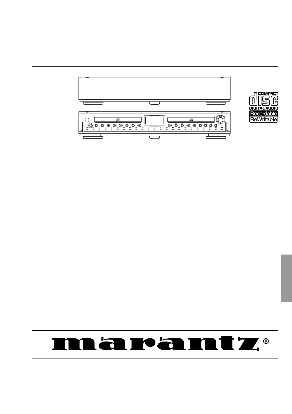
DR2100
DR2100DR2100
399K855010 AO
3120 785 22510
First Issue:2001.03
Page 2
MARANTZ DESIGN AND SERVICE
Using superior design and selected high grade components, MARANTZ company has created the ultimate in stereo sound.
Only original
it is famous.
Parts for your
ORDERING PARTS :
Parts can be ordered either by mail or by Fax.. In both cases, the correct part number has to be specified.
The following information must be supplied to eliminate delays in processing your order :
1. Complete address
2. Complete part numbers and quantities required
3. Description of parts
4. Model number for which part is required
5. Way of shipment
6. Signature : any order form or Fax. must be signed, otherwise such part order will be considered as null and void.
MARANTZ parts can insure that your MARANTZ product will continue to perform to the specifications for which
MARANTZ equipment are generally available to our National Marantz Subsidiary or Agent.
USA
MARANTZ AMERICA, INCMARANTZ AMERICA, INC.
440 MEDINAH ROAD
ROSELLE, ILLINOIS 60172
USA
PHONE : 630 - 307 - 3100
FAX : 630 - 307 - 2687
AMERICAS
SUPERSCOPE TECHNOLOGIES, INC.
MARANTZ PROFESSIONAL PRODUCTS
2640 WHITE OAK CIRCLE, SUITE A
AURORA, ILLINOIS 60504 USA
PHONE : 630 - 820 - 4800
FAX : 630 - 820 - 8103
AUSTRALIA
QualiFi Pty Ltd,
24 LIONEL ROAD,
MT. WAVERLEY VIC 3149
AUSTRALIA
PHONE : +61 - (0)3 - 9543 - 1522
FAX : +61 - (0)3 - 9543 - 3677
NEW ZEALAND
WILDASH AUDIO SYSTEMS NZ
14 MALVERN ROAD MT ALBERT
AUCKLAND NEW ZEALAND
PHONE : +64 - 9 - 8451958
FAX : +64 - 9 - 8463554
EUROPE / TRADING
MARANTZ EUROPE B.V.
P.O.BOX 80002, BUILDING SFF2
5600 JB EINDHOVEN
THE NETHERLANDS
PHONE : +31 - 40 - 2732241
FAX : +31 - 40 - 2735578
AUSTRALIA
TECHNICAL AUDIO GROUP PTY, LTD
558 DARLING STREET,
BALMAIN, NSW 2041,
AUSTRALIA
PHONE : 61 - 2 - 9810 - 5300
FAX : 61 - 2 - 9810 - 5355
THAILAND
MRZ STANDARD CO.,LTD
746 - 754 MAHACHAI ROAD.,
WANGBURAPAPIROM, PHRANAKORN,
BANGKOK, 10200 THAILAND
PHONE : +66 - 2 - 222 9181
FAX : +66 - 2 - 224 6795
TAIWAN
PAI- YUING CO., LTD.
6 TH FL NO, 148 SUNG KIANG ROAD,
TAIPEI, 10429, TAIWAN R.O.C.
PHONE : +886 - 2 - 25221304
FAX : +886 - 2 - 25630415
BRAZIL
PHILIPS DA AMAZONIA IND. ELET. ITDA
CENTRO DE INFORMACOES AO
CEP 04698-970
SAO PAULO, SP, BRAZIL
PHONE : 0800 - 123123
FAX : +55 11 534. 8988
(Discagem Direta Gratuita)
CANADA
LENBROOK INDUSTRIES LIMITED
633 GRANITE COURT,
PICKERING, ONTARIO L1W 3K1
CANADA
PHONE : 905 - 831 - 6333
FAX : 905 - 831 - 6936
SINGAPORE
WO KEE HONG DISTRIBUTION PTE LTD
130 JOO SENG ROAD
#03-02 OLIVINE BUILDING
SINGAPORE 368357
PHONE : +65 858 5535 / +65 381 8621
FAX : +65 858 6078
MALAYSIA
WO KEE HONG ELECTRONICS SDN. BHD.
SUITE 8.1, LEVEL 8, MENARA GENESIS,
NO. 33, JALAN SULTAN ISMAIL,
50250 KUALA LUMPUR, MALAYSIA
PHONE : +60 3 - 2457677
FAX : +60 3 - 2458180
JAPAN
MARANTZ JAPAN, INC.
35- 1, 7- CHOME, SAGAMIONO
SAGAMIHARA - SHI, KANAGAWA
JAPAN 228-8505
PHONE : +81 42 748 1013
FAX : +81 42 741 9190
Technical
KOREA
MK ENTERPRISES LTD.
ROOM 604/605, ELECTRO-OFFICETEL, 16-58,
3GA, HANGANG-RO, YONGSAN-KU, SEOUL
KOREA
PHONE : +822 - 3232 - 155
FAX : +822 - 3232 - 154
SHOCK, FIRE HAZARD SERVICE TEST :
CAUTION : After servicing this appliance and prior to returning to customer, measure the resistance between either primary AC
cord connector pins ( with unit NOT connected to AC mains and its Power switch ON ), and the face or Front Panel of product and
controls and chassis bottom.
Any resistance measurement less than 1 Megohms should cause unit to be repaired or corrected before AC power is applied, and
verified before it is return to the user/customer.
Ref. UL Standard No. 1492.
In case of difficulties, do not hesitate to contact the Technical
Department at above mentioned address.
001120 A.O
Page 3
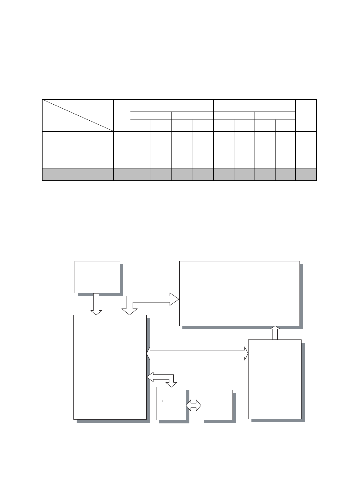
1. Servicing the DR2100
1.1 INTRODUCTION:
The DR2100 is the consumer version of a CD recorder, this means that the SCMS (Serial Copy Management System) is
included. The DR2100 can only record on the Audio CDRs (Consumer Use).
The DR2100 is suitable for recording and playback of CD-RW discs (CD-Re Writable disc).
Playback & Recording and Disc
Disc
Player/Recorder
Audio CD Player
Current products Ex:CD-17
Audio CD Player
CD-RW playback Ex:CD-17MK II
CD-RW Recorder
For Professional Ex:CDR630/640
CD-RW Recorder
For Consumer Ex:DR2100
CDR
CD
Consumer Disc
Finalized
non
Finalized
Professional Disc
Finalized Finalized
non
Finalized
Consumer Disc
Finalized
PP no P no no no no no -
PP no P no P no P no -
P P P/R P P/R P/R P/R P/R P/R no
P P P/R P P P/R P/R P YES
CD-RW
non
Finalized
Professional Disc
non
Finalized
P
SCMS
Consumer : For Digital Audio
Professional : For General use (Including PC)
P : Playback
R : Recording
1.2 OPENING THE PRODUCT:
The product can be opened by removing the top cover (6 screws). Once the product is opened one can have access to the
several PCB's and the main module.
Power Supply
PCB
CDR Module
MAR775
u-COM
PCB
DISPLAY
PCB
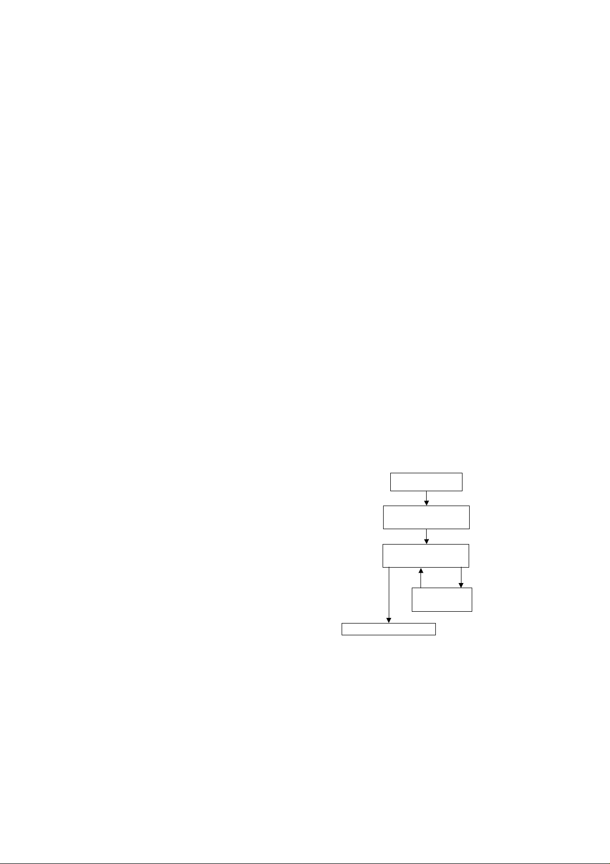
Below the several PCB's and it function and service policy will be discussed:
Rear Terminal
PCB
CD
Loader
MAR1250
1
Page 4

1.2.1 CDR loader (CDR main module CDL4009 or MAR775):
This complete CDR loader is considered as not repairable in the field. therefore this module will be repaired centrally. A
module exchange procedure will be set up for this purpose. The module can be removed from the product by removing 4
screws and the transformer and loosing the connectors.
This module is the complete CD recorder, it contains the following parts:
CD Mechanism (CDM4009'). Underneath this mechanism a PCB is mounted which is adjusted to the mechanism (laser
current settings are stored in EEPROM).
Loader Assy. This mechanical assy takes care for the tray control.
Main PCB. This PCB takes care that the (analog or digital) signal to be recorded is converted into a suitable signal which
can be recorded on the disc.
Digital signals with an other sampling frequency then 44.1kHz will be converted in the sample rate converter (DASP) to
44.1kHz.
Analog signals will be first converted into a digital converter by the AD converter.
This PCB also takes care that the signal from the CD (playback) is converted into a suitable digital signal (or analog via
the DA converter).
The main microprocessor controls the several functions of this PCB.
1.2.2 Power Supply PCB.
This PCB contains the Power SW, which is jointed the Power bottom on the front panel. This PCB consists of power supply
part. The power suppluy part delivers the several voltages for the diffrent PCB in the DR2100. On this power supply one
fuse (primary side) is mounted on this PCB. All parts are available as spare parts.
1.2.3 Terminal PCB.
This PCB coutaius input and output terminals. All parts are available as spare parts.
1.2.4 Display Board.
This PCB contains the Display, which informs the user about the status of the recording/playback process and it also takes
care for scanning the keys on the front panel. The information from the keys is fed via a I C connection to the main
microprocessor on the CDR loader module. Information which needs to be displayed is also fed via this I C line from the
main microprocessor on the CDR loader module to the display controller.
The parts for this PCB are available as service parts so this PCB can be repairable up to component level.
2
2
IMPORTANT
In case of replace the CD-R module "MAR775", the initialization is necessary.
Please initialize the CD-R module with following orders.
1. Press the POWER button (POWER ON) while depressing FINALIZE button and REC
TYPE button together.
2. LCD Display shows;
WAIT
PGM PROTOCOL
PGM PORT END
3. Press the POWER button (POWER OFF).
Then the CD-R module set up to DR2100 own status.
2
Page 5

2 TECHNICAL SPECIFICATIONS
GENERAL
System .................................................................................................... Compact disc digital audio
Number of channels ................................................................................ 2 (stereo)
Applicable discs ...................................................................................... CD, CD-R (digital audio), CD-RW (digital audio)
Power Requirement
Power Consumption................................................................................ 20 W
Operating Temperature .......................................................................... 5 - 35 °
Dimension (MAX)
Width ................................................................................................. 420 mm
Height................................................................................................ 76 mm
Depth ................................................................................................ 309 mm
Weight................................................................................................ 4.4 kg
AUDIO
Frequency Response.............................................................................. 20 Hz - 20 kHz
Playback S/N .......................................................................................... 100 dB
Playback Dynamic Range....................................................................... 96 dB
Playback Total Harmonic Distortion ........................................................ 0.003 %
Recording S/N......................................................................................... 90 dB
Recording Dynamic Range ..................................................................... 92 dB
Recording Total Harmonic Distortion ...................................................... 0.006 %
Digital Coaxial Output ............................................................................. 0.5 V (p-p) / 75 ohms
Analog Output Voltage ............................................................................ 2 V RMS
Digital Optical Output .............................................................................. - 20 dBm
............................................................................... AC 110 V - 240V 50 / 60 Hz
C
Recording values for line input
Digital Coaxial Input (automatic sample rate conversion)....................... 11 - 56 kHz
Digital Optical Input (automatic sample rate conversion)........................ 11 - 56 kHz
Analog Input ............................................................................................ 600 mVrms / 50 kohms
Specifications subject to change without prior notice.
3
Page 6
3. WARNINGS
WARNING
All ICs and many other semiconductors are susceptible to
electrostatic discharges (ESD). Careless handling during
repair can reduce life drastically.
When repairing, make sure that you are connected with the
same potential as the mass of the set via a wristband with
resistance. Keep components and tools at this potential.
ATTENTION
Tous les IC et beaucoup d´autres semi-conducteurs sont
sensibles aux décharges statiques (ESD). Leur longévite
pourrait être considérablement écourtée par le fait qu´aucune
précaution nést prise à leur manipulation.
Lors de réparations, s´assurer de bien être relié au même
potentiel que la masse de l´appareil et enfileer le bracelet
serti d´une résistance de sécurité.
Veiller à ce que les composants ainsi que les outils que l´on
utilise soient également à ce potentiel.
WARNUNG
Alle ICs und viele andere Halbleiter sind empfindlich
gegenüber elektrostatischen Entladungen (ESD).
Unsorgfältige Behandlung im Reparaturfall kann die
Lebensdauer drastisch reduzieren.
Sorgen Sie dafür, daß sie im Reparaturfall über ein Pulsarmband mit Widerstand mit dem Massepotential des
Gerätes verbunden sind.
Halten Sie Bauteile und Hilfsmittel ebenfalls auf diesem
Potential.
AVAILABLE ESD PROTECTION EQUIPMENT :
anti-static table mat large 1200x650x1.25mm 4822 466 10953
anti-static wristband 4822 395 10223
connection box (3 press stud connections, 1M ) 4822 320 11307
extendible cable (2m, 2M , to connect wristband to connection box) 4822 320 11305
connecting cable (3m, 2M , to connect table mat to connection box) 4822 320 11306
earth cable (1M , to connect any product to mat or to connection box) 4822 320 11308
KIT ESD3 (combining all 6 prior products - small table mat) 4822 310 10671
wristband tester 4822 344 13999
ESD
WAARSCHUWING
Alle IC´s en vele andere halfgeleiders zijn gevoelig voor
electrostatische ontladingen (ESD).
Onzorgvuldig behandelen tijdens reparatie kan de levensduur
drastisch doen vermindern. Zorg ervoor dat u tijdens reparatie
via een polsband met weerstand verbonden bent met hetzelfde
potentiaal als de massa van het apparaat.
Houd componenten en hulpmiddelen ook op ditzelfde potentiaal.
AVVERTIMENTO
Tutti IC e parecchi semi-conduttori sono sensibili alle scariche
statiche (ESD).
La loro longevità potrebbe essere fortemente ridatta in caso di
non osservazione della più grande cauzione alla loro
manipolazione. Durante le riparationi occorre quindi essere
collegato allo stesso potenziale che quello della massa
delápparecchio tramite un braccialetto a resistenza.
Assicurarsi che i componenti e anche gli utensili con quali si
lavora siano anche a questo potenziale.
small 600x650x1.25mm 4822 466 10958
Safety regulations require that the set be restored to its
original condition and that parts which are identical with
those specified be used.
Safety components are marked by the symbol
Les normes de sécurité exigent que l`appareil soit remis
à l`état d`origine et que soient utilisées les pièces de
rechange identiques à celles spécifiées.
Les composants de sécurité sont marqués
Bei jeder Reparatur sind die geltenden Sicherheitsvorschriften zu beachten. Der Originalzustand des Gerätes
darf nicht verändert werden. Für Reparaturen sind Originalersatzteile zu verwenden.
Sicherheitsbauteile sind durch das Symbol markiert.
U : VERSION N : VERSION
DANGER: Invisible laser radiation when open.
AVOID DIRECT EXPOSURE TO BEAM.
Varning !
Advarsel !
Osynlig laserstrålning när apparaten är öppnad och
spärren är urkopplad. Betrakta ej strålen.
Usynlig laserstråling ved åbning når sikkerhedsafbrydere
er ude af funktion. Undgå udsaettelse for stråling.
CLASS III b
LASER PRODUCT
SAFETY
Veiligheidsbepalingen vereisen, dat het apparaat in zijn
oorspronkeliijke toestand wordt teruggebracht en dat
onderdelen, identiek aan de gespecificeerde, worden toegepast.
De Veiligheidsonderdelen zijn aangeduid met het symbool
Le norme di sicurezza estigono che l´apparecchio venga
rimesso nelle condizioni originali e che siano utilizzati i
pezzi di ricambiago identici a quelli specificati.
Componenty di sicurezza sono marcati con
CLASS 3B
LASER PRODUCT
Varoitus !
Avatussa laitteessa ja suojalukituksen ohitettaessa olet alttiina
näkymättömälle laserisäteilylle. Älä katso säteeseen !
After servicing and before returning the set to customer
perform a leakage current measurement test from all
exposed metal parts to earth ground, to assure no
shock hazard exists.
The leakage current must not exceed 0.5mA.
"Pour votre sécurite, ces documents doivent être utilisés par
des spécialistes agréés, seuls habilités à réparer votre
appareil en panne".
4
Page 7
4. SERVICE HINTS AND TOOLS
SERVICE TOOLS
The tools listed below are standard test tools that can be used for repairing and testing Marantz
CD Players & Recorders.
Audio signals disc 4822 397 30184
Disc without errors (SBC444)+
Disc with DO errors, black spots and fingerprints (SBC444A) 4822 397 30245
Disc (65 min 1kHz) without no pause 4822 397 30155
Max. diameter disc (58.0 mm) 4822 397 60141
Torx screwdrivers
Set (straight) 4822 395 50145
Set (square) 4822 395 50132
13th order filter 4822 395 30204
Hexagon socket screw button (No. 1.5)
5
Page 8
5. SERVICE MODE
The plug is in the socket
Turn off the POWER
Press<POWER>while pressing
<ENTER>and<PLAY/PAUSE> of CD player
“SERVICE_1” is displayed
Press< >
STANDBY LED Light on RED
“POWER_LED” is displayed
Press< >
STANDBY LED Light on GREEN
“POWER_LED” is displayed
Press< >
All parts of LCD is turned on
Press< >
Press<ENTER>and<PLAY/PAUSE> of CD Player
Version of MAIN
“VER
-COM is displayed
” is displayed
Each Segment is displayed one by one
Press< >
Check of key
When key is depressed,key name is displayed
Shut off the power
6
Page 9
6. DIAGNOSTICS SOFTWARE
6.1 Dealer mode
The purpose of the dealer mode is to prevent people taking out
the CD inside the player at exhibitions, showrooms etc.. This
mode disables the open/close function of the player.
The dealer mode can be switched on and off pressing keys
[OPEN/CLOSE] and [STOP] of the CDR player simultaneously
while switching on the unit. The dealer mode is stored in the
flash memory and can only be changed by executing the above
actions.
6.2 Dealer diagnostics
DEALER DIAGNOSTICS
(status of player)
If power ON,
switch power OFF
Press <ENTER> + <FFWD>
simultaneously and switch
ON unit
6.2.2 Requirements to perfo rm the test
Working keyboard to start up the test.
Working local display to check the output messages.
Display blinks
“BUSY”
during test
NO
Set OK?
YES
Set displays
“
PASSED
To end test, switch OFF unit
6.2.1 Description
The intention of the dealer diagnostics is to give an indication
of the CDR player status. An inexperienced, even nontechnical dealer will/can perform the test. Tests are executed
automatically without need for external tools or disassembly of
the unit. This test checks the CDR main board using the same
tests as the electrical service diagnostics program. Only the
result of the test, "PASSED" or "ERROR", will be shown on the
display. Pressing keys [F FWD] and [REWIND] simultaneously
while switching on the unit, starts the test. Switching off the uni t
ends the test.
”
Figure 6-1
Set displays
“ERROR”
CL96532086-024.eps
090999
7
Page 10
6.3 Electrical service diagnostics
ELECTRICAL SERVICE DIAGNOSTICS
(software versions, test for defective components)
If power ON,
switch power OFF
Load CD-DA disc (SBC444A)
Press <ENTER> + <CD STOP>
simultaneously and switch ON unit
PLAYER
INFORMATION
Display :
"PLAYER ID"
"SW VERSION BACK END"
"SW VERSION CDR LOADER"
"SW VERSION CD LOADER"
CDR MAIN
BOARD TEST
Display :
"DTST1"
DRAM test (7702)
PASS OR FAIL
Display :
"DTST2"
FLASH CHECKSUM test (7702)
PASS OR FAIL
Display :
"DTST3"
FLASH ERASE test (7702)
PASS OR FAIL
Display :
"DTST4"
CODEC test (7702)
PASS OR FAIL
Display :
"DTST5"
CDR LOADER
COMMUNICATION test
PASS OR FAIL
Display :
"DTST6"
CD LOADER
COMMUNICATION test
PASS OR FAIL
*
ABORT TEST
ABORT TEST
ABORT TEST
ABORT TEST
ABORT TEST
Press <F FWD>
Press <F FWD>
Press <F FWD>
Press <F FWD>
Press <F FWD>
ABORT TEST
Press <F FWD>
ABORT TEST
Press <F FWD>
LOADER TESTS
CDR LOADER TEST
CD-DA disc must be loaded
Display shows current disc time
Test OK?
YES
CD LOADER TEST
CD-DA disc must be loaded
Display shows current disc time
Test OK?
YES
DISPLAY TEST
DISPLAY TEST
Display segments blink at f=1kHz
KEYBOARD &
RC TEST
KEYBOARD & RC TEST
Display shows name of pressed keys
Press <F FWD>
NO
NO
Display :
or
or
Display :
or
or
"BERR1"
"NO CDDA"
"NO DISC"
Press <F FWD>
"BERR2"
"NO CDDA"
"NO DISC"
Press <F FWD>
Tests OK?
YES
NO
Display :
"DERRn"
n = failed test
Display next
failed test
Figure 6-2
8
To end test, switch OFF unit
CL 96532086_025.eps
080999
Page 11
6.3.1 Description
The intention of the electrical service diagnostics is to show the
software versions present in the player and to direct the dealer
towards defective internal units. The units are : the CDR main
board, the CDR loader, the CD loader in case of a DR6050 and
the keyboard/display board. A sequence of tests is executed
automatically. Some of the te sts can be aborted or skipped
without the result being taken into account. External tools or
disassembly of the unit is not necessary to get the diagnostic
information. Pressing keys [ENTER] and [CD STOP].
simultaneously while switching on the unit, starts the test.
Switching off the unit ends the test.
6.3.2 Requirements to perform the test
Working keyboard t o st art up the test.
Working loc al display to check the output messages.
A CD-DA disc with a minimum of 3 tracks in all trays to
perform the disc test.
6.3.3 Description of the tests
disc test is executed to check focus control, disc motor control,
radial control and jump grooves control. The d isc test is
performed by audio play-back of 5 seconds at the beginning,
middle and end of the disc.
CDR loader test
During the test, the current disc time is shown. In case of an
error the message "BERR1" will be displayed and the [F FWD]
key must be pressed to continue with the following test.
Pressing the [F FWD] key also aborts this test.
CD loader test
During the test, the current disc time is
shown.
In case of an error the message "BERR2" will be
displayed and the [F FWD] key must be pressed to continue
with the following test. Pressing the [F FWD] key also aborts
this test.
Display test
All segments will blink at a frequency of 1 Hz. Pressing the [F
FWD] key will start the next test because the user has to check
for himself if all segments work properly.
Player information
In this part of the test the following important information can be
checked without removing the cover :
Recorder ID.
SW-version back end of player.
SW-ver sion CDR loader.
SW-version CD loader.
CDR main board test
[F FWD] key. The message "DERRn" will be displayed with n
indicating the faulty test number.
If one of the tests is aborted with the [F FWD] key, no error
message will be displayed for this test. The flash data erase
test ("DTST3") can not be aborted !
The CDR main board test consists out of :
DRAM test
Display : "DTST1". The DRAM used for buffer management is
tested by writing, reading and verifying test patterns.
Flash checksum test
Display : "DTST2". This test checks the checksum of the
player's SW stored in the flash.
Flash data erase
Display : "DTST3". During this test, all temporary information
(CDtxt) in the flash is erased.
CODEC (ADC/DAC) test
Display : "DTST4". This test checks the CODEC IC by writing,
reading and verifying test patterns.
CDR communication test
Display : "DTST5". The communication between the host
processor (DASP) and the CDR loader via the DSA-R-bus is
tested.
Keyboard and remote control tests
The test will give the user the ability to test every key without
executing the function assigned to it. Therefore, the user needs
to press every key on the keyboard and the remote control. The
display will show the name of the key being pressed. Pressing
more than one key at once will give an unpredictable result
except for the service combinations : [ENTER] + [DISPLAY],
[ENTER] + [CD STOP], [ENTER] + [F FWD], [ENTER] +
[MENU], [ENTER] + [CANCEL], [ENTER] + [CD PLAY].
6.4 Mechanical service diagnostics
MECHANICAL SERVICE DIAGNOSTICS
(test for defective components)
If power ON,
switch power OFF
Press <ENTER> + <DISPLAY>
simultaneously and switch
ON unit
FOCUS TEST
Display shows
To end test, switch OFF unit
6.4.1 Description
“BUSY”
Visual inspection
SLEDGE TEST
Visual inspection
Display shows
<FWD><REWIND>
“BUSY”
Figure 6-3
CL96532086_026.eps
080999
CD communication test
Display : "DTST6"). The communication between the host
processor (DASP) and the CD loader is tested.
Loader tests
These tests determine if the CDR loader and the CD loader in
case of a DR2100 work correctly. A CD-DA disc with a
minimum of 3 tracks needs to be inserted in both loaders. A
No external tools are required to perform this test. The cover
needs to be removed because the user has to check the
movements of the tray, focus and sledge visually. Pressing
keys [ENTER] and [DISPLAY] simultaneously while
switching on the unit, starts the test. Switching off the unit ends
the test. In case of a DR2100, one can check the CD loader
mechanics in the same way by pressing the above key
combination on the CD player keys.
9
Page 12
6.4.2 Requirements to perform the test
6.5.1 Description
Working keyboard to cycle through the tests and to start up
the test.
Working local display to check the output messages.
6.4.3 Description of the tests
Focus control test
The focussing lens is continuously moving up and down. The
display reads "BUSY".
Sledge control test
After pressing [F FWD] the sledge continuously moves up and
down. Pressing [REWIND] stops the sledge at the position it is
in and the focus control test resumes. The display reads
"BUSY".
6.5 DC-er ase se rvice mode
DC ERASE SERVICE MODE
(erasement of complete CD-RW)
Load CD-RW disc
Press
<ENTER> + <MENU/STORE>
simultaneously and switc h
ON unit
This test is initiated by pressing [ENTER] and [MENU/STORE]
simultaneously while switching on the unit. The player will
erase a complete CD-RW disc (including PMA and ATIP lead
out area) at speed N=2. The display shows the countdown of
the remaining time required for the operation to complete. The
format is "ER mm:ss", where "mm" are the remaining minutes
and "ss" the remaining seconds. After completion the message
"PASSED" is shown, and the player has to be switched off and
on again to start up in normal operating mode. Switching off the
unit before completion of the test, leaves the disc in an
unpredictable state. In such case only a complete DC-erase
procedure can recover the CD-RW disc.
6.5.2 Requirements to perform the test
Functional CDR player.
A CD-RW audio disc must be present in the tray.
Display shows:
mm
ER mm:ss
“
:remaining minutes
”
ss :remaining seconds
TOTAL
and
REM
are also
illuminated
Display shows:
“
PASSED
”
when the erase function is
completed
ERROR
“
”
if DC ERASE fails
To end test, switch OFF unit
CL96532086_027.eps
Figure 6-4
080999
10
Page 13
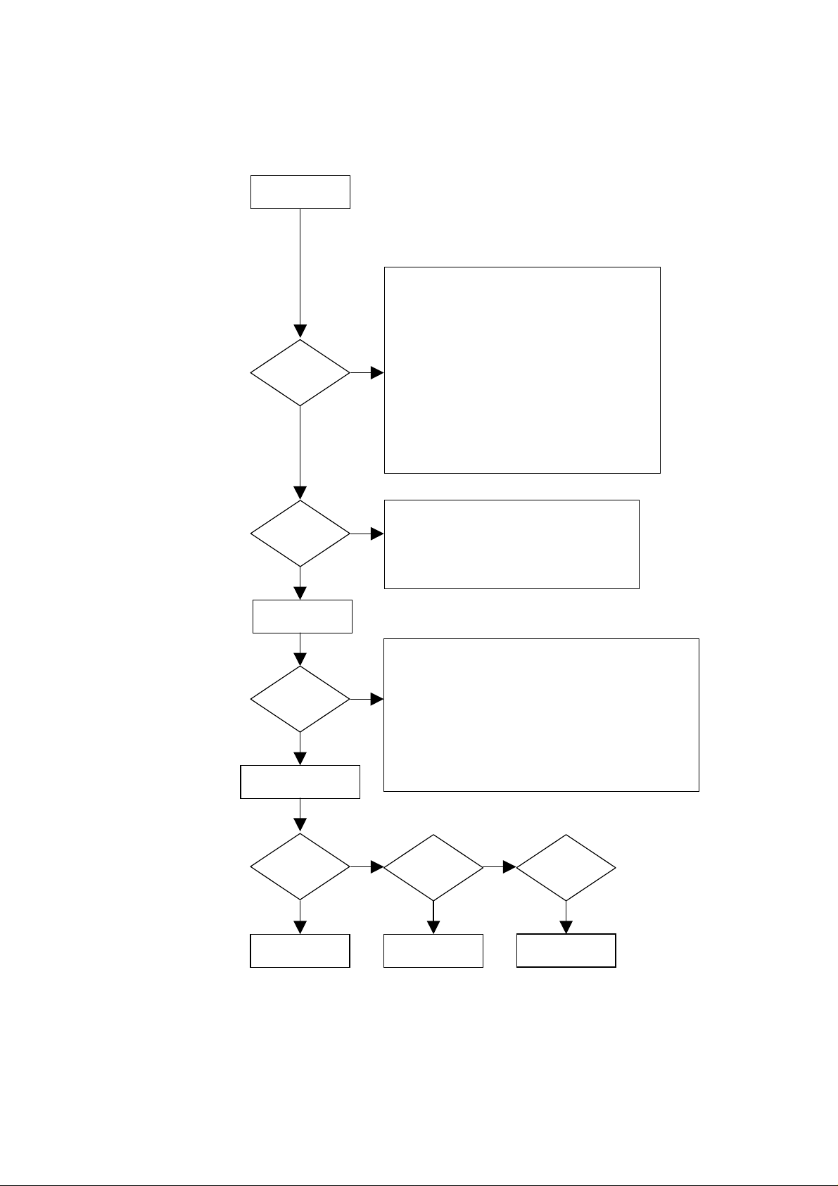
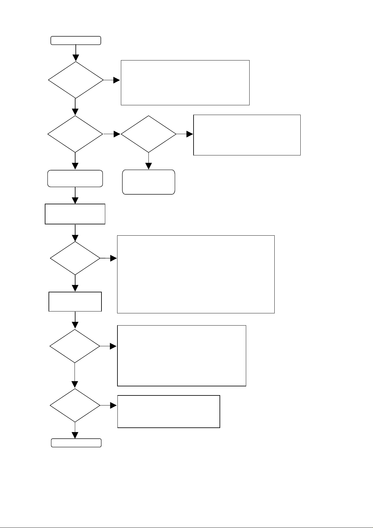
7. Faultfinding trees
7.1 C DR-Module (MAR775)
NO DISC LOADED
SWITCH ON POWER
DISPLAY?
YES
NO
CHECK:
MAINS, MAINS CABLE
POWER SUPPLY (SEE FAULT FINDING GUIDE PSU)
DISPLAY (SEE FAULT FINDING GUIDE DISPLAY BOARD)
WIRING
ON/OFF SWITCH
FUSES
VOLTAGES
WIRING
SUPPLY VOLTAGES
CLOCK SIGNAL 8MHz
CONTROL SIGNALS
KEYBOARD
STANDBY LED
ELECTRICAL SERVICE DIAGNOSTICS:
DISPLAY TEST, KEYBOARD TEST
DISPLAY:
"INSERT DISC"
YES
PRESS
<OPEN/CLOSE>
TRAY?
YES
INSERT DISC
PRESS <OPEN/CLOSE>
CD-DA DISC
LOADED?
CHECK:
NO
NO
WIRING
POWER SUPPLY VOLTAGE S
ELECTRICAL SERVICE DIAGN O STICS:
REPLACE CDR MODULE IF
OR
"BERRn"
CHECK:
DISPLAY BOARD (SEE FAULT FINDING GUIDE DISPLAY BOARD)
MECHANICAL SERVICE DIAGNOSTICS:
REPLACE CDR MODULE IF ERROR OCCURS
CD-R DISC
LOADED?
YESYES
ERROR OCCURS
WIRING
SUPPLY VOLTAGES
CLOCK SIGNAL 8MHz
CONTROL SIGNALS
KEYBOARD
ELECTRICAL SERVICE DIAGNOSTICS:
DISPLAY TEST, KEYBOARD TEST
NONO
"DERRn"
CD-RW DISC
LOADED?
YES
SEE CD-DA DISC
FAULT FINDING
SEE CD-R DISC
FAULT FINDING
Figure 7-1
11
SEE CD-RW DISC
FAULT FINDING
CL 96532076_016.eps
290799
Page 14
CD-DA DISC LOADED
DISC
DETECTION &
READING?
YES
DISPLAY:
“CD”
&
T.O.C. INFO?
NO
NO
CHECK:
WIRING
POWER SUPPLY VOLTAG E S
ELECTRICAL SER VICE DIAG N O STICS:
REPLACE CDR MODULE IF
OR
"BERRn"
CHECK:
DISC: DIRT, SCRATCHES, DAMAGED...
ELECTRICAL SER VICE DIAG N O STICS:
REPLACE CDR MODULE IF
OR
"BERRn"
ERROR OCCURS
ERROR OCCURS
"DERRn"
"DERRn"
YES
PRESS <PLAY>
ANALOG
AUDIO
OUT?
YES
DISTORTION?
NO
HEADPHONE?
YES
DIGITAL
AUDIO
OUT?
YES
NO
YES
NO
NO
CHECK:
AUDIO CONNECTIONS & CABLES
REAR TERMINAL BOARD
W651 CONNECTION
FLEX CONNECTION
+5V (pin 8 conn. JJ01)
KILL VOLTAGE (pin 7 conn. JJ01):
-8V DURING PLAY
KILL TRANSISTORS QN51 - QN52
PLAY AUDIO SIGNAL S DI SC TRACK 15 :
SIGNAL OF 5.4 VPP ON PINS 1 AND 3 OF CONN.
JJ02
ELECTRICAL SER VICE DIAG N O STICS:
REPLACE CDR MODULE IF
OR
"BERRn"
CHECK:
AUDIO CONNECTIONS & CABLES
REAR TERMINAL BOARD
ELECTRICAL SER VICE DIAG N O STICS:
REPLACE CDR MODULE IF
OR
"BERRn"
CHECK:
WIRING OF HEADPHONE/IR BOARD
ELECTRICAL SER VICE DIAG N O STICS:
REPLACE CDR MODULE IF
OR
"BERRn"
CHECK:
AUDIO CONNECTIONS & CABLES
REAR TERMINAL BOARD
ELECTRICAL SER VICE DIAG N O STICS:
REPLACE CDR MODULE IF
OR
"BERRn"
ERROR OCCURS
FLEX CONNECTION
+5V (pin 8 conn. JJ01)
ERROR OCCURS
ERROR OCCURS
FLEX CONNECTION
+5V (pin 8 conn. JJ01)
DIGITAL OUT TRANSFORMER LT02, Q311
ERROR OCCURS
"DERRn"
"DERRn"
"DERRn"
"DERRn"
PLAY BACK OF CD-DA
DISCS OK
Figure 7-2
CL 96532076_017.eps
290799
12
Page 15
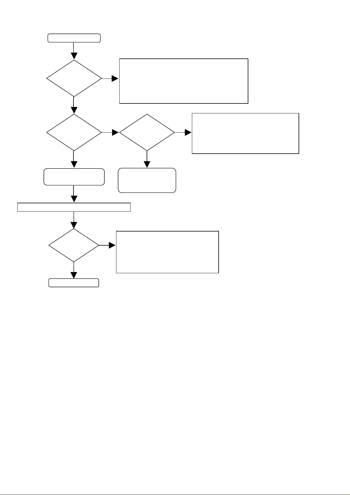
CD-R DISC LOADED
DISC
DETECTION &
READING?
YES
DISPLAY:
“CD R”
OPC INFO?
&
YES
NO
NO
CHECK:
WIRING
POWER SUPPLY VOLTAG ES
ELECTRICAL SERVICE DIAGNOSTICS:
REPLACE CDR MODULE IF
OR
"BERRn"
ERROR OCCURS
"DERRn"
CHECK:
DISPLAY:
“CD”
&
T.O.C. INFO?
NO
YES
DISC: DIRT, SCRATCHES, DAMAGED...
ELECTRICAL SER VICE DI AGNOSTICS:
REPLACE CDR MODULE IF
OR
"BERRn"
ERROR OCCURS
"DERRn"
CD-R DISC PARTIALLY
RECORDED OR EMPTY
START MANUAL
RECORDING FROM
ANALOG SOURCE
LEVEL
ADJUSTABLE?
YES
START RECORDING
FROM DIGITAL
SOURCE
DIGITAL IN?
OPTICAL IN?
YES
NO
NO
FINALISED CD-R DISC
LOADED
SEE CD-DA DISC
FAULT FINDING
CHECK:
AUDIO CONNECTIONS & CABLES
DISPLAY BOARD (SEE FAULT FINDING GUIDE DISPLAY BOARD)
EASY JOG KNOB
I2C COMMUNICATION
ELECTRICAL SERVICE DIAGNOSTICS:
KEYBOARD TEST
ELECTRICAL SER VICE DI AGNOSTICS:
REPLACE CDR MODULE IF
OR
"BERRn"
ERROR OCCURS
"DERRn"
CHECK:
AUDIO CONNECTIONS & CABLES
I/O BOARD
FLEX CONNECTION
+5V (pin 8 conn. JJ01)
Q311, OPTICAL RECEIVER J301
ELECTRICAL SER VICE DI AGNOSTICS:
REPLACE CDR MODULE IF
OR
"BERRn"
ERROR OCCURS
"DERRn"
RECORDING
SUCCESSFUL?
YES
SET OK
NO
CHECK:
ELECTRICAL SERVICE DIAGNOSTICS:
REPLACE CDR MODULE IF
OR
"BERRn"
ERROR OCCURS
"DERRn"
Figure 7-3
13
CL 96532076_018.eps
290799
Page 16
CD-RW DISC LOADED
DISC
DETECTION &
READING?
YES
DISPLAY:
“CD RW”
&
OPC INFO?
YES
NO
NO
CHECK:
WIRING
POWER SUPPLY VOLTAGES
ELECTRICAL SERVICE DIAGNOS TICS:
REPLACE CDR MODULE IF
OR
"BERRn"
ERROR OCCURS
"DERRn"
CHECK:
DISPLAY:
“CD”
&
NO
T.O.C. INFO?
YES
DISC: DIRT, SCRATCHES, DAMAGED...
ELECTRICAL SERVICE DIAGNOS TICS:
REPLACE CDR MODULE IF
OR
"BERRn"
ERROR OCCURS
"DERRn"
CD-RW DISC PARTIALLY
FINALISED CD-RW DISC
RECORDED OR EMPTY
START ERASING OF LAST RECORDED TRACK
CHECK:
ERASING
NO
SUCCESSFUL?
YES
SET OK
LOADED
SEE CD-DA DISC
FAULT FINDING
ELECTRICAL SERVICE DIAGNOS TICS:
REPLACE CDR MODULE IF
OR
"BERRn"
ERROR OCCURS
"DERRn"
IF DISC CORRUPTED TRY DC ERASE
Figure 7-4
CL 96532076_019.eps
290799
14
Page 17

7.2 CD Module
CD MODULE
NO DISC
POWER ON
DISC
DETECTION
STARTS?
YES
DISPLAY?
YES
PRESS
<OPEN/CLOSE>
NO
NO
CHECK FLEX CONNECTION FROM CDR MAIN BOARD
POWER SUPPLY
+5V, +12V AT TESTPOINTS 28 AND 27
+5V AT CONN. 1000 PINS 1 AND 3
+5V AT IC7005 PIN 14
+3V3 AT IC7000 PINS 5,17,21,57, CHECK SAFETY RESISTORS
+5V AT IC7020 PIN 25
+10V AT IC7020 PINS 26, 27, 28
+12V AT IC7021 PIN 5, CHECK SAFETY RESISTOR R3131
+12V AT IC7022 PIN 5, CHECK SAFETY RESISTOR R3154
+5V AT IC7025 PIN 16
+5V AT IC7202 PIN 38, CHECK SAFETY RESISTOR R3308
+3V3 AT IC7309 PINS 4 AND 13, CHECK SAFETY RESISTORS R3215, R3216
+12V AT IC7120 PIN 8, CHECK SAFETY RESISTOR R3263
CLOCKS
8.4672MHz AT TESTPOINT 7
12MHz AT TESTPOINTS 29 AND 30
11.2896 AT TESTPOINT 10
2.1168MHz AT TESPOINT 20
44.1kHz AT TESTPOINT 21
DISPLAY
SEE FAULTFINDING GUIDE DISPLAY BOARD
MICROPROCESSOR 7202
NO
TRAY?
YES
LOAD DISC
(CD-DA OR PARTIALLY
RECORDED CD-R/CD-RW)
PRESS <OPEN/CLO S E >
NO
TOC?
YES
SEE NEXT PAGE:
PLAYBACK
DIAGNOSTIC SOFTWARE : MECHANICAL SERVICE DIAGNOSTICS CD LOADER : TRAY TEST
CHECK TRAY MOTOR VOLTAGES
MICROPROCESSOR 7202
CHECK T RAY MOTOR DRIVER IC7021
REPLACE OR REPAIR CD LOADER ASSY:
TRAY MOTOR ASSY 02, BELT 11
DIAGNOSTIC SOFTWARE : MECHANICAL SERVICE DIAGNOSTICS CD LOADER :
CHECK WIRING TO CDM
CHECK POWER DRIVERS 7021, 7022, 7020
CHECK VOLTAGES ON POWER DRIVERS (SEE CIRCUIT DIAGRAMS)
TESTPOINTS 4, 5, 6 : PULSE DENSITY MODULATED SIGNALS
HF PATH
TESTPOINTS 1, 2, 3, 9 : EYEPATTERN
CHECK
CDRW DISC. EYEPATTE RN OF CDRW DISC WI LL BE AMP LIFIED (
EYEPATTERN OF CDDA DISC WILL BE ATTENUATED(
CHECK
TESTPOINTS 20, 21, 22: I2S
REPLACE OR REPAIR CD LOADER ASSY (CDM MECHANISM)
RW
S1,S2
FOCUS TEST & SLEDGE TEST
AT TESTPOINT 8 : HIGH FOR CDDA AND CDR DISC, LOW FOR
AT TESTPOINTS 25 AND 26 (SEE CIRCUIT DIAGRAMS)
TRAY+, TRAY-
DATA, WCLK, SCLK
»
X 0.8)
»
X 2.5).
CL 96532086_030.eps
080999
Figure 7-5
15
Page 18

CD MODULE PLAYBACK
PRESS <PLAY>
DAC 7309
AUDIO?
YES
NO
OPAMP 7120
TESTPOINTS 20, 21, 22 : I2S AT INPUT OF DAC 7309
CHECK POWER SUPPLY PINS 4, 13
CHECK CLK11 AT PIN 6 : 11.2896MHz
PIN 11 : MUTE HIGH?
TESTPOINTS 23, 24 : ANALOG OUTPUT?
REP LACE DAC 7309
TESTPOINTS 23, 24 : ANALOG OUTPUT?
POWER SUPPLY: PIN 8 12V
REP LA CE OPAMP 7120
DISTORTION?
NO
AUDIO
CD OUT PCB?
YES
PLAYBACK CD
MODULE OK
YES
NO
DAC 7309
OPAMP 7120
FLEX TO CDR MAINBOARD
FLEX TO CD OUT BOARD
CHECK I/O BOARD, CD OUT BOARD
Figure 7-6
CL 96532086_031.eps
080999
16
Page 19

Dimmer Control
The -controller, MB90F553A/MB90553A adjust the brightness of LCD back light by receiving
signal from IR or SYSTEM BUS.
Mode LCD_DIM (1Pin) LCD_BL (2Pin)
Backlight OFF Low Low
Backlight ON Low High
Dimmer ON High Low
8. Faultfinding Guide
8.1 D isplay Boar d
8.1.1 Description of display board
General description
The display board has three major parts : the LCD (Liguid
Crystal Display), the display controller and the
The display controller is controlled by the DASP master
processor on the CDR main board. The communication
protocol used is I2C. So all the information between DASP and
display controller goes via the SDA or I2C DATA and SCL or
I2C CLK lines. Communication is always initiated by the DASP
on the CDR main board. Unlike the previous generations of
CDR players, the interrupt generated by the display controller
at key-press or reception of remote control is not used. Instead,
the DASP polls the display controller for these events.
B
lock Diagram around µ-Com
keyboard.
MB90550A
LCD DISPLAY
LCD
Control
Line
LED
on/stadby/timer
LED
Drive
Lines
LCD DRV.
Keyboard
KEY
SW.
Control
Lines
LCD DRV.
Control
Line
Extra
Extra Key
SW.
Keyboard
HOST
DASP
IIC Bus
Front
u-COM
Control
Lines
RC-5/SYSTEM
Bus in
Resister
Matrix
Player
Type
Select
Lines
Easyjog
Control
Lines
EASYJOG
RC-5
SYSTEM
Bus in/out
SYSTEM
Bus out
Key Input
Each key is detected by changing the voltage level shown below.
3.5V <4.5V 2.5V <3.5V 1.5V <2.5V 0.5V <1.5V <0.5V
KEY0 (P38) PROGRAM CANCEL/DELITE MENU/STORE DISPLAY DOOR OPEN
KEY1(P39) CD
PLAY/PAUSE
KEY2(P40) SOURCE REC TYPE REC CDR STOP
KEY3(P41) CDR
PLAY/PAUSE
If this recorder is STANDBY state, the power will be recovered when the key is pressed.
Stop Key can be work to select either CDR or CD.
CD STOP
CD/CDR FF CD/CDR REW CD TRAY
(CD SELECT)
(CDR SELECT)
ERASE FINALISE CDR
OPEN/CLOSE
OPEN/CLOSE
STAND BY
TRAY
ENTER
P20/A16
P21/A17
P22/A18
P23/A19
P24/A20
P25/A21
P26/A22
P27/A23
P30/ALE
P31/RD
P32/WRL
P33/WRH
P34/HRQ
P35/HAK
P36/RDY
P37/CLK
P40/SCK
P41/SOT
P42/SIN
P43/SCK1
P44/SOT1
P45/SIN1
P46/ADTG
P47/SCK0
P50/SDA0/SOT0
P51/SCL0/SIN0
P52/SDA1
Pin Configuration
P17/AD15
100
1
2
3
4
5
6
7
8
9
10
11
V
SS
12
13
14
15
16
17
18
19
20
21
22
V
CC
23
24
25
26
C
27
28
29
30
31323334353637383940414243444546474849
P53/SCL1
P16/AD14
P15/AD13
P14/AD12
P13/AD11
P12/AD10
P11/AD09
P10/AD08
P07/AD07
P06/AD06
P05/AD05
P04/AD04
P03/AD03
P02/AD02
P01/AD01
P00/AD00
P64/AN4
P65/AN5
P66/AN6
P67/AN7
VCCX1X0V
MD0
P70/IRQ0
P71/IRQ1
99989796959493929190898887868584838281
CC
AV
P55/SCL2
P54/SDA2
AVRH
AVRL
SS
AV
P60/AN0
P61/AN1
P62/AN2
P63/AN3
SS
V
(FPT-100P-M06)
SS
50
MD1
80
79
78
77
76
75
74
73
72
71
70
69
68
67
66
65
64
63
62
61
60
59
58
57
56
55
54
53
52
51
PA4/CKOT
PA3
PA2
RST
PA1/OUT3
PA0/OUT2
P97/PPG5
P96/PPG4
P95/PPG3
P94/PPG2
P93/PPG1
P92/PPG0
P91/OUT1
P92/OUT0
P87/IN3
P86/IN2
P85/IN1
P84/IN0
P83/TOT1
P82/TOT0
P81/TIN1
P80/TIN0
P77/IRQ7
P76/IRQ6
P75/IRQ5
P74/IRQ4
P73/IRQ3
P72/IRQ2
HST
MD2
-COM DESCRIPTION
Pin PORT SIGNAL I/O DESCRIPTION
1 P20/A16 LCD_DIM O LCD back light of DIMMER Control See DIMMER Control
2 P21/A17 LCD_BL O LCD backlight ON/OFF See DIMMER Control
3 P22/A18 POWER_LED O Power ON LED Active H
4 P23/A19 STB_LED O Standby LED Active H
5 P24/A20 SYS_SW I When Bus Switch SYSTEM bus = H
6 P25/A21 SYS_MUTE O SYSTEM LINE OUT OF MUTE Active H
7 P26/A22 STB_MUTE O Power On < - > MUTE when STANDBY
8 P27/A23 CDR/Through O To switch AUDIO OUT DR; H, Through; L
9 P30/ALE N.C. I
10 P31/RD N.C. I
11 VSS GND
12 P32/WRL N.C. I
13 P33/WRH N.C. I
14 P34/HRQ N.C I
15 P35/HAK N.C. I
16 P36/RDY POWER_ON O Power Control Power ON; H
17 P37/CLK N.C. I
18 P40/SCK TCK. I/O To connect Flash Writer
19 P41/SOT SYS_OUT
20 P42/SIN SYS_IN
21 P43/SCK1 N.C. I
22 P44/SOT1 N.C. I
23 VCC +5STB -- VCC
24 P45/SIN1 N.C. I
25 P46/ADTG N.C. I
26 P47/SCK0 N.C. I
27 CC
28 P50/SDA0/SOT0 ROM_SDA I/O SERIAL DATA to EEPROM
29 P51/SOL0/SIN0 ROM_SCL O SERIAL DATA to EEPROM
30 P52/SDA1 IIC_DATA I/O DATA Communication to CDR Module
31 P53/SCL1 IIC_CLK I/O CLK Communication to CDR Module
32 P54/SDA2 N.C. I
33 P55/SCL2 N.C. I
34 AVCC +5STB -- VCC
35 AVRH +5STB -- VCC
36 AVRL GND
37 AVSS GND
38 P60/AN0 KEY_IN_0 I KEY_0 INPUT
39 P61/AN1 KEY_IN_1 I KEY_1 INPUT
40 P62/AN2 KEY_IN_2 I KEY_2 INPUT
41 P63/AN3 KEY_IN_3 I KEY_3 INPUT
42 VSS GND
43 P64/AN4 N.C. I
44 P65/AN5 N.C. I
45 P66/AN6 N.C. I
46 P67/AN7 N.C. I
47 P70/IRQ0 LT1 I RESET signal from CDR Active H
48 P71/IRQ1 N.C. I
49 MD0 TMODE I To changing CPU Mode PULL UP
50 MD1 MD1 I To changing CPU Mode PULL UP
51 MD2 TAUX3 I To changing CPU Mode PULL DOWN
52 HST HST I STANDBY input signal by hardware PULL UP
53 P72/IRQ2 D_MOTOR_REV O Door REV Motor ON Active H
54 P73/IRQ3 D_MOTOR_FWD O Door FWD Motor ON Active H
55 P74/IRQ4 D_OPEN_SW I Door Open Active L
56 P75/IRQ5 D_CLOSE_SW I Door Close Active L
57 P76/IRQ6 JOG_A I JOG A
58 P77/IRQ7 JOG_B I JOG B
59 P80/TIN0 INT. I INTERRUPT signal from CDR Module
60 P81/TIN1 N.C. I
61 P82/TOT0 N.C. I
62 P83/TOT1 N.C. I
63 P84/IN0 IR_IN I Control bus INPUT either IR/RC5 or
64 P85/IN1 IN_SW I CDR, CD trey hardware SW. Active : H / Passive : L
65 P86/IN2 CDR_IN I CDR Trey IN Active L
66 P87/IN3 CD_IN I CD Trey IN Active L
67 P90/OUT0 N.C. I
68 P91/OUT1 N.C. I
69 P92/PPG0 N.C. I
70 P93/PPG1 N.C. I
71 P94/PPG2 N.C. I
72 P95/PPG3 N.C. I
73 P96/PPG4 N.C. I
74 P97/PPG5 N.C. I
75 PA0/OUT2 N. C. I
76 PA1/OUT3 N. C. I
77 RST CPU_RST I CPU RESET signal Low (PULL UP)
78 PA2 N.C. I
79 PA3 N.C. I
80 PA4/CKOT N.C. I
81 VSS GND
82 X0 8MHz X’tal
83 X1 8MHz X’tal
84 VCC +5STB -- VCC
85 P00/AD00 TAUX I To Flash Writer
86 P01/AD01 --- I To change CPU mode PULL UP
87 P02/AD02 RST O LCD Driver RESET Active L
88 P03/AD03 LCD_/WR O WR OUTPUT to LCD Driver Active L
89 P04/AD04 LCD_/RD O RD OUTPUT to LCD Driver Active L
90 P05/AD05 A0 O LCD Driver mode See NJU6450 Data Sheet
91 P06/AD06 N.C. I
92 P07/AD07 N.C. I
93 P10/AD08 D0 I/O To LCD Driver
94 P11/AD09 D1 I/O To LCD Driver
95 P12/AD10 D2 I/O To LCD Driver
96 P13/AD11 D3 I/O To LCD Driver
97 P14/AD12 D4 I/O To LCD Driver Active L
98 P15/AD13 D5 I/O To LCD Driver Active L
99 P16/AD14 D6 I/O To LCD Driver Active L
100 P17/AD15 D7 I/O To LCD Driver See NJU6450 Data Sheet
TRXD
TTXD
is activate
O SYSTEM Control bus OUTPUT
To connect Flash Writer
I SYSTEM Control bus or IR/RC5 Input
To connect Flash Writer
IIC Interface
IIC Interface
SYSTEM
Active H
Figure 8-1
17
18
Page 20

RST
D
0~D7
A
E (RD)
R/W (RD)
Block Diagram
NJU6450A
Reset
0
MPU Interface
Instruction
Status
BF
Bus
Holder
Decoder
Page Address
Multiplexer
Register
Com. Address
Register
Counter
Com. Address
Staet Line Register
I / O Buffer
Page Address Decoder
Display
2560 bit
Data RAM
Culumn Decoder
0b1b2b3b4b5b6b7
b
Line Decoder
Line Counter
Displey
Timing
Generator
V
DD
V1V2V3V4V
Display Data Latch
5
. V
4
. V
1
, V
DD
V
Common
Timing
Generator
5
. V
3
. V
2
, V
DD
V
5
V
SS
Driver
Segment
Driver
Common
SEG
0
~SEG
COM0~COM
60
15
VSS
D0
D1
D2
D3
D4
D5
D6
D7
VDD
RST
FR
V
5
V3
V2
M/S
V
4
V1
COM0
COM1
COM2
COM3
COM4
COM5
COM6
Pin Configuration
R/W (WR)
E (RD)
OSC2OSC1A0SEG0
SEG1
SEG2
76
100
SEG3
SEG4
SEG5
NJU6450A
2
2
FR
M/S
SEG6
SEG7
SEG8
SEG9
SEG10
SEG11
SEG12
SEG13
SEG14
SEG15
SEG16
SEG17
SEG18
SEG19
5175
50
26
251
SEG20
SEG21
SEG22
SEG23
SEG24
SEG25
SEG26
SEG27
SEG28
SEG29
SEG30
SEG31
SEG32
SEG33
SEG34
SEG35
SEG36
SEG37
SEG38
SEG39
SEG40
SEG41
SEG42
SEG43
SEG44
OSC
OSC
COM7
COM8
COM9
COM10
COM11
COM12
COM13
COM14
COM15
SEG60
SEG59
SEG58
SEG57
SEG56
SEG55
SEG54
SEG53
SEG52
SEG51
SEG50
SEG49
SEG48
SEG47
SEG46
SEG45
19 20
Page 21

8.1.2 Test instructions
Clock signal
As clock driver for the display controller, a resonator of 8 MHz
(XY01) is used. The signal can be measured at pins 8 and 9 of
the display controller : 8 MHz ±5%.
I2C DATA/I2C CLK
These lines connect to the DASP master processor via
respectively pin 5 and pin 7 of conn. JU02
. When there is no
communication, they should have the high level (+5V). The
oscillogram below gives an indication of how these signals
should look like.
IR receiver - remote control
In the DR2100 the IR receiver RPM6934 (ZY83, ZY84) is
mounted on the display board. In all versions the IR receiver
connects to the display controller. The signal coming from the
receiver can be checked at pin 3 of conn. JU05. This
signal is
normally high (+5V). When the remote control is being
operated, pulses mixed in with the +5V can be measured. The
oscillogram gives an indication of how the signal looks like with
the RC being operated.
+5V
I2C DATA
0V
+5V
I2C CLK
0V
CH1! 2. 00 V =
CH2 2 V= M TB10.0ms ch 1+
CL 96532076_025.eps
Figure 8-2 ‘I2C signals’
290799
+5V
+5V
0V
-35V
0V
1
CH1! 2.00 V= MT B20. 0ms ch 1+
Figure 8-3 ‘IR receiver signal’
CL 96532076_021.eps
290799
21
Page 22

8.1.3 Display board troubleshooting guide
SWITCH POWER ON,
EXIT STAND BY
MODE
DISPLAY?
NO
YES
CHECK :
SUPPLY VOLTAGES
+5V
5 % at conn. JU04-1
CLOCK SIGNAL
8Mhz at pins 82, 83 of QU01
CONTROL SIGNALS
RESET IN 3V3 (high) at conn. JU02-4 after start up
I2C DATA at conn. JY01-5
I2C CLK at conn. JY01-7
ELECTRICAL SERVICE DIAGNOSTICS - Local display test
KEY
NO
FUNCTIONS?
YES
REMOTE
NO
CONTROL?
YES
FRONT, MAIN u-COM BOARD
OK
CHECK:
KEY LINES
ELECTRICAL SERVICE DIAGNOSTICS – Keyboard test
EASY JOG KNOB
CHECK:
IR RECEIVER signal at pin 63 of QU01
ELECTRICAL SERVICE DIAGNOSTICS – Remote control test
CL 96532076_020.eps
290799
Figure 8-4 Display board troubleshooting’
22
Page 23

8.2 Power Supply Unit P816
8.2.1 Troubleshooting P816
Chec
k fuse F820 and
replace if necessary
OK
Check DC voltages
5VM, 5VU, +12V, -8V
NO
Disconnect power supply unit from CDR main board,
Main u-com board and REAR TERMINAL board.
Connect resistor 1k ohm at pin 3 of conn. J852 and ground
These voltages might be somewhathigher than specified
Check : Waveform of D804 at anode
Turn input voltage up and check voltageacross C821,
this voltage should be
t
Check DC voltages
5VM, 5VU, +12V, -8V
R830, R825, R826, R890 is not shorted.
Q825 works properly.
NO
Connect the mains inlet to a mains
isolated variac
1.41 x Vin AC
OK
OK
OK
OK
NO
Power supply unit OK
Power supply is OK
Check : - CDR main board
- Main u-com board
-C
D main board
- REAR TERMINAL board
Check the path of the other faulty voltage(s)
+5VM: check D856, C857, L856, C859, Q851
+5VU : check CR890, D866, L867, Q852, C853, C858, C867
+12V : check D866, C867, L867, Q861, R861, R862, C863
Check the functionality of the following components :
F820, R819, C820, L820, D802
OK
Power supply OK?
8.3 CD Main Board
The CD main board is built around the compact disc
mechanism MAR1250 and a loader 1250. The CDM delivers
diode signals and an unequalised high frequency signal. These
signals are necessary inputs for the decoder CD10. Based on
these signals the decoder will control the disc. The decoder is
able to control the sledge, focus motor, radial motor and turn
table. When everything is "locked", the decoder delivers a
digital output according to IEC958 standard, subcode to the
microprocessor and I2S for reproducing analog audio signals
by means of a D/A converter.
Check :
YES
Load on secondary output
Overvoltage protection : L832, D814, C814, R814, R815, R816
Oscillator voltage on pin 10 of Q810 :
check C802, R810 replace Q810
Drive circuit : gate voltage of MOSFET Q825
components R812, R813, C813, R825
Regulation circuit
- Measure voltage on pin 6 of Q810 with oscilloscope
- If > 2.5V check the regulation circuit : Q810, D881
R881- R885, C881, C882, R804 - R806, R809, C804, C809
Figure 8-5
The microprocessor controls the CD10 and is slave of the
master processor on the CDR main board in the DR2100. Both
processors communicate via a DSA connection (data, strobe
and acknowledge).
23
Page 24

CDM VAM1250
Trig enta
HF amp.
Diode signals
Radial, focus
Motor, sledge
CD10
SERVO
DECODER
Loader assy
PROCESSOR
UDA1320
DAC
Figure 8-6
8.3.1 Supply Voltages
Description
The CD main board receives +5V and +12V from the CDR main
board via respectively pin 16 and pin 15 of connector 1208. The
+5V is split up into +5VHF and +5V. The +5VHF is used mainly
for the diode currents and the HF-amplifier. The +5V is used for
the digital part of the board. On the board a +3V3 is made from
the +5V for the decoder CD10 and an A3V3 for the DAC
UDA1320. The +12V is split up into A12V for the audio output
stage and +12V for the power drivers of the CDM.
Measurements
Connect following supplies to next pins :
+5V + 5% to pin 16 of connector 1208.
+12V + 5% to pin 15 of connector 1208.
Ground reference to pin 17 of connector 1208.
Keep microprocessor 7202 in reset by forcing pin 7 of
connector 1208 to +5V. Check the following voltages :
Point Voltage
Position 1000 pins 1,3
Position 7000 pins 5,17,21,57
Position 7005 pin 14
Position 7020 pins 25
Position 7020 pins 26,27,28
Position 7021 pin 5
Position 7022 pin 5
Position 7025 pin 16
Position 7202 pin 38
Position 7309 pins 4,13
Position 7120 pin 8
+5V
+3.
+5V
+5V
+10
+12V
+12V
+5V
+5V
+3V
+12V
±
5%
3V± 5%
±
5%
±
5%
±
10%
±
10
±
10
±
5%
±
5% ( ot
3 ± 5%
±
10
her appl. 3V3 possible)
Figure 8-7
8.3.2 Clock Signals
Description
The microprocessor has its own Xtal or resonator of 12MHz.
The CD10 needs a clock of 8.4672MHz + 100ppm. This speed
also relates to the disc speed. To avoid locking proble m s
between the two drives in the CDR775, both drives run on the
same clock. Therefore the CD main board gets the clock for the
decoder from the CDR main board via pin 2 of connector 1208.
The DAC needs a system clock to drive its internal digital filters
and to clock the I2S signals from the decoder. In our case this
is 11.2896MHz (CL11) generated by the CD10.
Measurements
Connect the power supply as described above in "1.1.1.
Supply Voltages".
DSA
IIS, DOBM
ANA OUT
CL96532086_048.eps
CL96532086_049.eps
080999
Connect on pin 2 of position 1208 a clock signal of 8.4672
MHz ( 100ppm minimum rise time of 50ns and at TTL level
(0V and +5V).
Keep microproces sor 7202 in reset by forcing pin 7 at
position 1208 to +5V.
Release the reset. Now, the processor will reset the CD10
for at least 75
µs.
The output clock CL11 should be available now at pin 42 of
the CD10.
Check the following frequencies :
080999
Point Frequency
Position 7000 pin 16
Position 7202 pins 14,15
Position 7309 pin 6
Position 7309 pin 1
Position 7309 pin2
8.4672 MHz
12MHz
11.2896 MHz
2.1168 MHz
44.1kHz
Figure 8-8
8.3.3 CD10 Decoder/Servo SAA7324 (7000)
Description
The CD10 is a single chip combining the functions of a CD
decoder, digital servo and bitstream DAC. The decoder/servo
part is based on the CD7. The decoding part supports a full
audio specification and can operate at single speed (n=1) and
double speed (n=2).
Block Diagram
V
V
SSA2
DDA2
V
V
DDA1
4 14 5 17 33 50 58 52 57
PRE-
PROCESSING
DIGITAL
PLL
EFM
SRAM
RAM
VERSATILE PINS
INTERFACE
63 34 61 62 32
V1
V2/V3V4 V5 KILL
V
SCL
SDA
RAB
SILD
HFIN
HFREF
ISLICE
TEST1
TEST2
TEST3
SELPLL
CRIN
CROUT
CL16
CL11/4
SBSY
SFSY
SUB
RCK
STATUS
RESET
D1 D2 D3 D4
8910
12
R1
13
R2
V
7
GENERATOR
40
39
41
42
2
1
FRONT
3
6
25
31
44
24
16
15
TIMING
26
49
48
47
46
45
43
CONTROLLER
38
END
TEST
DECODER
INTERFACE
ref
MICROCONTROLLER
MICRO-
RIN
I
ref
ADC
INTERFACE
V
SSA1
11
DEMODULATOR
ADDRESSER
SUBCODE
PROCESSOR
Figure 8-9
V
SSD2
SSD1VSSD3
CONTROL
PART
AUDIO
PROCESSOR
PEAK
DETECT
±
5%
±
CONTROL
FUNCTION
KILL
±
100ppm
±
100ppm
±
100ppm
100ppm
V
DDD1(P)VDDD2(C)
CONTROL
CORRECTOR
INTERFACE
INTERFACE
(LOOPBACK)
INTERFACE
BITSTREAM
CL96532086_050.eps
OUTPUT
STAGES
MOTOR
ERROR
FLAGS
EBU
SERIAL
DATA
SERIAL
DATA
DAC
CL96532086_051.eps
080999
54
55
56
64
59
60
53
51
30
29
28
27
37
35
36
20
21
18
19
22
23
080999
RA
FO
SL
LDON
MOTO1
MOTO2
CFLG
DOBM
EF
SCLK
WCLK
DATA
SCLI
WCLI
SDI
V
neg
V
pos
LN
LP
RN
RP
24
Page 25

Pin Configuration
Figure 8-10
8.3.4 TDA7073A Power Drivers (7021, 7022)
Description
The TDA7073A is a dual power driver circuit for servo systems
with a single supply. In this configuration it is used to drive the
sledge, tray, focus and radial.
Measurements
Keep microprocessor 7202 in reset by forcing pin 7 of
connector 1208 to +5V. Connect the power supply as
described above in "1.1.1. Supply Voltages". Check the
following voltages :
Figure 8-11
Figure 8-12
8.3.5 BA6856FP Turn Table Motor Driver (7020)
Description
This component is a 3 phase, full wave pseudo linear driving
system with inbuilt Hall Bias circuit and 3 phase parallel output.
Measurements
Keep processor 7202 in reset by forcing pin 7 of connector
1208 to +5V. The outputs 9, 10, 11 of connector 1006 are 0V.
Pin 21 of the motor driver 7020 is 2.5V 10%.
Pin 22 of the motor driver 7020 is 2.5V 10%.
Pin 23 of the motor driver 7020 is 0V.
Pin 19 of the motor driver 7020 is 5V
10%.
Put the processor out of reset to continue the measurement.
Check MOT1 at pin 59 of CD10. The duty cycle of the output
should be 50%. Check wave form at pin 11 of 7005-D :
amplitude 5V + 5% duty cycle 50%.
The motor driver 7020 can be measured dynamically by
connecting a hall motor to the application panel. Apply a pulse
of 1V 10Hz and 15% duty cycle to pin 22 (Ec) as input value
with reference to pin 21 (Ecr=2.5V). Measure the output signals
on the driver. This will give as response a square wave on pin
17 and pin 18. When a positive voltage is applied, the square
wave on pin 17 will go ahead of the square wave on pin 18.
All signals will have a value as shown in the truth table. Check
the following output signals :
1
2
3
4
5
6
7
8
9
10
11
12
13
14
15
16
171819202122232425262728293031
32
33
34
35
36
37
38
39
40
41
42
43
44
45
46
47
48
514950
52
53
54
55
56
57
58
59
60
61
62
63
64
HFREF
HFIN
ISLICE
V
SSA1
V
DDA1
I
ref
V
RIN
D1
D2
D3
D4
R1
R2
V
SSA2
CROUT
CRIN
VDDA2
LN
LP
V
neg
V
pos
RN
RP
SELPLL
TEST1
CL16
RA
FO
SL
DOBM
SAA7324
V
SSD3
MOTO1
SFSY
SBSY
RCK
SUB
V
SSD1
V5
V4
V2/V3
KILL
EF
DATA
WCLK
V
DDD1(P)
SCLK
TEST3
CL11/4
RAB
SCLI
TEST2
SDI
WCLI
V
SSD2
SILD
MOTO2
STATUS
V
DDD2(C)
CFLG
V1
RESET
LDON
SDA
SCL
CL96532086_052.eps
080999
Pin Location Value
5 7021
12V
10%
5 7022
12V 10%
1 7022
1.65V
10%
2 7022
1.65V 10%
6 7022
1.65V 10%
7 7022
1.65V 10%
1 7021
5.0 10%
2 7021
5.0 10%
6 7021
1.65V 10%
7 7021
1.65V
10%
CL96532086_053.eps
080999
Pin Location Value DC
9 7022 FOC
5.8V
± 10%
12 7022 FOC 5.8V
13 7022 RAD 5.8V
16 7022 RAD 5.8V
9 7021 SLE 5.8V
12 7021 SLE 5.8V
13 7021 TRAY- 5.8V
16 7021 TRAY+ 5.8V
CL96532086_054.eps
080999
25
Page 26

Motor controller truth table
Input conditions conn 1006 pin Outputs conn 1006 Test points on driver
684 732 9 10 11 18 17 16
U+ U- V+ V- W+ W- UCOIL VCOIL WCOIL HALL_U HA LL_V HALL_W
L M H M M M 6V 0V 0V 0V 5V
H M L M M M 0V 6V 6V 5V 0V
M M L M H M 0V 6V 0V 0V 5V
M M H M L M 6V 0V 6V 5V 0V
H M M M L M 0V 0V 6V 5V 0V
L M M M H M 6V 6V 0V 0V 5V
CL96532086_055.eps
Figure 8-13
Hall-elements input signal voltage
levels
Input voltage Level Tolerance Unit
H2.80.1V
M2.50.1V
L2.20.1V
CL96532086_056.eps
Figure 8-14
8.3.6 Tray Control
080999
080999
Description
The tray control consists of a TDA7073A power driver (7021)
controlled by the processor 7202 via pin 19 TRAYIN and pin 20
TRAYOUT. If pin 20 is low and pin 19 high, the TRAY+ signal
at pin 16 of 7021 is forced to +8V and the TRAY- signal at pin
13 of 7021 to GND : the tray will open. If pin 20 is high and pin
19 low, TRAY+ becomes GND and TRAY- becomes +8V : the
tray will close. If pin 19 and 20 of the processor have the same
value, TRAY+ and TRAY- will have the same value as well : the
tray stops moving.
Measurements
Keep procesor 7202 in reset by forcing pin 7 of connector 1208
to +5V. Connect a load of 15 , 7W between pin 3 and 4 of
connector 1002. Check the voltage over the load with TRAY+
(pin 3) as positive reference. Check also the levels of pins 19
and 20 of the processor.
U TRAY+,TR AY- = <100mV
Pin 20 = +5V
Pin 19 = +5V
Force pin 20 of the processor to ground, and check the
voltages.
U TRAY+,TRAY- = -6.5V( 10%
Pin 20 = +0V
Pin 19 = +5V
Force pin 19 of the processor to ground as well and check the
levels again.
U TRAY+,TR AY- = <100mV
Pin 20 = +0V
Pin 19 = +0V
Release pin 20 of the processor and check the levels.
U TRAY+,TRAY- = 6.5V( 10%
Pin 20 = +5V
Pin 19 = +0V
Release pin 19 of the processor and check the levels again:
U TRAY+,TR AY- = <100mV
Pin 20 = +5V
Pin 19 = +5V
26
Page 27

8.3.7 HF Path
Description
The pre-amplified HF-signal is presented to both n=1 and n=2
amplifier circuits. The mux/demux switches via software and
micro processor controlled S1 and S2 lines between either one
of the amplified n=1 or n=2 signals. The signal will then follow
another amplification and filtering circuit. The filtering again is
controlled by the S1 and S2 lines, dependant on whether the
disc starts up (speed n=1, S1 and S2 Low), disc plays at speed
n=1 (S1 Low, S2 High) or disc plays at speed n=2 (S1 and S2
High).
E AMP
n-dependant filtering
n=1 AMP
3174
3173
430R
430R
F157
2
2140
HFGND
2143
330p
n=2 AMP
3191
430R
3192
430R
2164
180p
2162
HFGND
180p
100p
+5VHF
3188
3203
+5VHF
2K7
7009
BFS20
2K7
HFGND
3169
3180
2K7
7023
BFS20
2K7
HFGND
HFGND
DUAL 4 CHANNEL
MUX/DEMUX
+5VHF
HFGND
2141
2n2
2146
1n5
16
7
8
1
5
2
4
12
14
15
11
74HCT4052D
VCC
VEE
GND
0
1
2
3
+5VHF
HFGND
390p
2149
680p
2130
100n
HF
47u
22n
2160
HFGND
HFGND
1K
3196
HF
BC848B
BC858B
7010
HFGND
2161
7007
HFGND
7025
10
0
0
4x
9
3
1
6
G4
22n
HFGND
3
2137
HFGND
HF
F156
9
3189
13
F313
390R
22n
HFGND
HFIN
3178
2138
1K
S1
S2
HFGND
HFGND
2142
22n
F310
2150
47n
3
7000
SAA7324
F309
1 HFREF
2145
2 HFIN
47p
3181
3 ISLICE
22K
F159
5
VSSA14
VDDA1
FRONT
END
HF
3193
180R
10K
3205
CL96532086_057.eps
080999
DC Settings
Set the power and reset connections as described above in
"1.1.1. Supply Voltages". Check the following voltages :
Force Pin Location Measure
Emitter 7006 2.4 10%
S1 and S2 “HIGH” Collector 7010 1.9 10%
S1 and S2 “LOW” Collector 7010 1.9 10%
S1 and S2 “HIGH” 13 7025 1.6 10%
S1 and S2 “LOW” 13 7025 1.6 10%
S1 and S2 “HIGH” 3 7025 3.2 10%
S1 and S2 “LOW” 3 7025 3.2 10%
CL96532086_058.eps
Figure 8-16
Figure 8-15
080999
27
Page 28

Transfer Characteristics
Set the power and reset connections as described above in
"1.1.1. Supply Voltages". Connect a function generator via a
serial resistor of 1k5 to pin 4 of connector 1000. Use the
S1 and S2 “low” S1 and S2 “high”Frequencies
Input V
AC
Pin 2 at 7000 Input V
300 Hz 200mV < 100mV ± 20% 200mV < 100mV ± 20%
10 kHz 200mV 295mV ± 20% 200mV 330mV ± 20%
100 kHz 200mV 310 mV ± 20% 200mV 330 mV ± 20%
300 kHz 200mV 385 mV ± 20% 200mV 335 mV ± 20%
800 kHz 200mV 655 mV ± 20% 200mV 485 mV ± 20%
1.5 MHz 200mV 1. 1V ± 20% 200mV 760 mV ± 20%
3MHz 200mV 1.1V ± 20% 200mV 1.1V ± 20%
Figure 8-17
function generator as a sine wave generator with output level
of 1Vtt. Check this AC value with an AC mV-meter connected
to the input (pin 2) of the CD10 (7000) :
AC
Pin 2 at 7000
CL96532086_059.eps
080999
HFDET Setting
Set the power and reset connections as described above in
"1.1.1. Supply Voltages". Connect a function generator via a
serial resistor of 1k5 to pin 4 of connector 1000. Use the
Location Voltage DC Voltage AC
No HF HF
F190 4.8V± 20% 4.8V± 20% 175mV± 20%
F192 < 100mV 1.1V± 20% F206 4.9V± 20% 150mV± 20% -
8.3.8 Audio Part - DAC
Description
The DAC used, is the UDA1320 bit stream, continuous
calibration. I2S signals from various formats can be entered at
pins 1,2 and 3. If these signals are in phase with the delivered
system clock at pin 6, the DAC will reproduce analog output
signals at pins 14 and 16. 0dB level is 0.85Vrms. These analog
signals are at 1.65Vdc level.
The DAC has features which can be checked on the input pins.
Mute will switch off the analog signals. De-emphasis is not
used, since this is done in the decoder. Attenuation of -12dB is
not used because this is also done in the decoder.
I2S
I2S is a kind of digital audio format, consisting out of 3 lines :
CLOCK, WORDSELECT and DAT A.
Figure 8-18
WS
function generator as a sine wave generator with output level
of 500 kHz, 1Vtt. Check this AC value with an AC mV-meter :
CL96532086_060.eps
080999
signal is in phase with the WS-signal. Transition of the WS
always happens on a falling edge of the CLK.
DATA
DATA contains all data-bits. Data bits are set by the
transmitting device, and read by the receiving device. The
position of the DATA-bits within the WS-signal is very
important. There are several formats for this. In our case we
always use Philips I2S format, no Japanese or Sony format.
The number of data-bits per channel depends on the used
devices.
Timing of the I2S-bus, in case of Philips I2S is shown in the
next figure :
LEFT SAMPLE RIGHT SAMPLE
WORD-SELECT
Word select (WS) indicates whether the data-sample is from
the left or the right audio-channel. It has the same frequency as
the sample rate of the digital audio signal. This can be 32, 44.1
or 48kHz. Normal polarity is low for a left sample and high for a
right sample. So within the low state of the WS-line the data bits
for the left channel are transferred, and within the high state the
data bits of the right channel are transferred.
CLOCK
The CLOCK signal (CLK) indicates when DataTips must be
set, and when DataTips must be read. The frequency depends
on the speed of the I2S-bus, but is always a factor of the
frequency of the WS-signal. It can be 48x, 64x, 96, 128x... .In
our case it is 48x the sample rate frequency = 2.1168MHz. The
28
CLK
DATA
Figure 8-19
MSBMSB
CL96532086_061.eps
080999
Page 29

Measurements
IIS
22
DAC AMPLIFIER
CLK 11
25
NMUT E
Keep processor 7202 in reset by forcing pin 7 of connector
1208 to +5V. This puts the processor outputs in tristate. Check
the reset at pin 4 of processor 7202 to make sure that the
processor is in reset.
Now, force port 0-4 pin 33 at 7202 to 0V to set the decoder
outputs (SCLK, WCLK, DATA, and CL11).
Check the MUTE pin 11 at 7309 : this pin should be low.
Connect via an I2S generator I2S-signals to the DAC :
Pin 1 at 7309: SLCK.
Pin 2 at 7309: WCLK.
Pin 3 at 7309: DATA.
Connect also the SYSCLK pin 6 at position 7309 to a clock
±
signal of 11.2896 MHz
Generate an I2S signal equivalent with a sine wave of 1kHz at
0dB for both left and right channels.
Check if 0.8 VRMS at pins 14 and 16 at location 7209 with a
DC of 1.65VDC.
Check if 1.7 VRMS
1209.
Force MUTE Pin 11 at 7309 high.
Measure again at pins 1 and 3 at location 1209 : both signals
should be at -90 dB.
100ppm.
±
2 dB at connector pins 1and 3 at location
Figure 8-20
1200 - 17
1200 - 19
CL96532086_062.eps
080999
29
Page 30

9. WIRING DIAGRAM
DISMOUNTING ADDITIONAL CABLES
W651
De-soldering and remove cables W651 from the loader
PCB.
+ side 2430
+ side 2424
REMARK When replace the CDR module MAR775 to
the new one. It is necessary to add removed cables at
same positions as follows;
WHITE + side lead of capacitor 2424
PINK + side lead of capacitor 2430
....
.....
30
Page 31

WY02
PY76
OPEN/CLOSE_PCB
JY08
PY36
JOG_PCB
JY10
WU10
PP16
1209
J682
WU08
WU09
WU09
MODULE
CD
1208
WC02
FLAT
JJ01
REAR_TERMINAL_PCB
CD_KEY_PCB
WC03
FLAT
PY26
WU03
JF52
WU05
WU05
JU05
JU08
JU03
JU04
JJ02
W651
JU09
JU10
WU04
J753
DISPLAY
WY03
PY66
JU06
JU07
JU01
JU11
MAIN_U-COM_PCB
JU01
JU02
PU16
J852
W853
J853
DOOR
JY01
WU01
FLAT
WU02
POWER_SUPPLY_PCB
1708
1500
J851
CDR
W851
FRONT_PCB
PY16
MODULE
1705
STANDBY
WU07
WU06
1400
WC01
FLAT
P801
J802
W802
P826
J803
AC_OUTLET_PCB
MOTER
PY46
SW
PCB
JY07
PY56
IR_SENSER_PCB
JY06
SIGNALS OF EACH WIRES
W851(J851 TO CDR MODULE) WU04(J852 TO JU04) WU10(JY10 TO JU10)
1 +5V 1 +5V 1 PULSE
2 2 GND 2 PULSE
3 3 STANDBY 3 KEY
4 GND 4 GND 4 GND
5 +5V
6 +5V
7 GND
5 +12V
WU01(JY01 TO JU01)
WU05(TO JU05)
8 GND 1 KEY2
9 GND 1 5V 2 KEY3
10 +12V 2 GND 3 5VM
11 -8V 3 RC-5 4 5VM
5 GND
W802(J802 TO J803) WU06(JY06 TO JU06)
6 GND
1 COLD 7 WR
2HOT 15V 8RD
2 GND 9 D1
WU02(JU02 TO CD MODULE)
3 RC-5 10 A0
1 5VM 11 D0
2
3
4 RESET IN
5 IIC DATA
6 GND
7 IIC CLK
8 INTERRUPT
9 GND
WU07(JY07 TO JU07)
1 STANBY
2 RED
3 GND
4 GRN
WU08(JY08 TO JU08)
12 D2
13 D3
14 BLOF
15 RST
16 D7
17 D6
18 D5
19 D4
20 DIMR
1 GND
WU03(JF52 TO JU03) 2 KEY0 W651
1 INT/EXT
WU09(TO JU09)
1 CDROUT RIGHT
2 RC-5 IN 2 GND
3 RC-5 OUT 1 GND 3 CDROUT LEFT
4 SUS SW 2 KEY1
5 SYS MUTE 3 KEY0
WC01
6 STB MUTE
7 DU/THROUGH
WC02
1
8 GND 2
1 KILL 3
2 GND 4 REC IN RCH
W853 3 CD DOBM 5 GND
4 GND 6 REC IN LCH
1 +12V 5 CD LCH 7 MUTE
2 GND 6 GND 8 5V
7 CD RCH 9 GND
10 OPT IN
11 COAX IN
12 GND
13 DOBM OUT
14 GND
31
32
Page 32

10. BLOCK DIAGRAM
CDL 4009
LOADER ASSY
CDM3800
M
TURN
TABLE
LASER
&
FORWARD
SENSE
PHOTO
DIODES
RADIAL
FOCUS
M
SLEDGE
M
TRAY
TRAY
SWITCH
FLEX 11P
FLEX 30P
FLEX 10P
2 WIRES
2 WIRES
CDR MAIN BOARD
1330
DRIVE, HALL FEEDBACK
1000
IR, IW, IE
CAHF
A1LF, A2LF, B1LF, B2LF
C1LF - C4LF
RAD+, RADFOC+, FOC-
PCS PRE-AMP
NE532D
1220
SIN+, SINCOS+, COS-
1200
SL+, SL-
TR+,TR-
TRAYSW
POWER
DRIVER
BA5938FM
EFMTIM3
LO9805
EFM TIMING
GENERATOR
CONTROL
LINES
LASER
CONTROL
CONTROL
LINES
AEGER
TZA1020
ANALOG
ERROR SIGNAL
GENERATOR
FOR
RECORDABLE
7225
7240
RAD
FOCUS
SLEDGE
TRAY
7008
EFMDATA, EFMCLK, LWRT
CONTROL
LINES
7016
CONTROL
LINES
XDAC
M62364
CONTROL
LINES
7010
2
I C BUS
ALPHA0
A1, A2, CALF
TLN, MIRN, FEN, REN, RE
REFSIN, SINPHI, REFCOS, COSPHI
VRA, VFO, VSL
TRAYIN, TRAYOUT
TRAYSWF
HALL
MOTOR
DRIVER
BA6856FP
7330
MOTOR CONTROL
HIN WOBBLE OFFTRACK
HF AMP
FILTER
7207
2
I C
EEPROM
M24C08
MACE2
SAA7399
BASIC ENGINE
PROCESSOR
CDR60
SAA7392
DECODER
ENCODER
LLP
CDR60PLL
ATIPSYNC
SYS-CLK-BE
(8.4672 MHz)
7300
MAD0-MAD7
MA8-MA17
CONTROL
LINES
7270
ADDRESS
BUSS
DOBM-CDR
SUBCODE BUS
2
I S BUS 1
DATA
BUS
DSA-CDR
FLASH
EPROM
DEMUX
FLASH
DRAM
A1 - A20 D16 - D31
DASP
MCF5244
DIGITAL AUDIO
SIGNAL
PROCESSOR
7802
33.8688 MHz
RAM
7208
7209
7703
ROM
7702
ADDRESS
BUS
1707
7701
DATA
BUSS
INT-COPY-ANA
SEL-HP-OUT
SYS-CLK-11W
2
I C BUS 2/4
L3 BUS
EXT-DIG-IN
DIG-OUT-C
EXT-OPT-IN
SYS-CLK-16W (16.9344 MHz)
SYS-CLK-BE
(8.4672 MHz)
DIGITAL
POT
DS1807
7405
CODEC
UDA1341TS
ADC / DAC
DSA-CD
2
I C BUS 3-CD
DOBM-CD
/2
74F74D
SYS-RESET
7801
ANALOG
IN
7406
7706A
2
I C BUS
ANALOG
OUT
ANA-OUT
CD-ANA-OUT
7409
7401
EXT-ANA-IN
CD-ANA-OUT
7407 7408
SYS-RESET
SYS-CLK-SW (8.4672 MHz)
+12N
1500
+5V
-3V
+5V
D5V
1706
11 WIRES
F934
10 WIRES
1410
1400 JJ01
FLEX 14P
FLEX 22P
JU02
1206
J851
POWER SUPPLY
FRONT BOARD
LCD DISPLAY
DISPLAY
DRIVER
QU01
u-COM
MB90553A
MAIN
u-COM
BOARD
IR IR
REAR TERMINAL
BOARD
CD PLAYER
7309
DAC
UDA1320
7207
uP
S87C654
7000
DECODER
SAA7324
1209
FLEX
7P
J682
CD OUT
BOARD
DRIVE
KEYS
RC5
3 WIRES3 WIRES
CD
J853
4 WIRES
2 WIRES
4 WIRES
3 WIRES
8 WIRES
RC-5
EXTERNAL
ANALOG IN
ANALOG OUT
COMMON
EXTERNAL
DIGITAL IN
DIGITAL OUT
COMMON
EXTERNAL
OPTICAL IN
CD
ANALOG OUT
CD
DIGITAL OUT
2 WIRES
EASY
JOG
DOOR
OPEN/CLOSE
SW.
Stand By SW./
Stand By LED
KEYS
J753
33 34
Page 33

11. SCHEMATIC DIAGRAM AND PARTS LOCATION
RY22
ZY83
PY56
ZY84
PY66
PY16
LLM
PLAY
SY23
47/6.3V
MOTORDOOR
RY01
56K
SY01
RY07
56K
STANDBY
DY05
GRN
CY83
CY84
47/6.3V
D_MOTOR
D_CLOSE_SW
D_OPEN_SW
SY02 SY04SY03
REC TYPE
RY09
18K
ERASE
PY46
RED
RY85
150
RY83
150
RY86
150
RY84
150
RY24
2.2K
OPTION
5V
RY23
1K
RY31
18K
RY04RY02
18K18K
RECSOURCE
RY30
18K
RY10
18K
FINALISE
JY07
S4B-EH
STANDBY
1
RED
2
GND
3
GRN
4
WU07
EHR4-EHR4
JY06
S3B-PH
3
2
1
WU06
PHR3-PHR3
3
WU05
PHR3-3P SAN
1
2
3
4
5
6
WM01
RY18
470
RY25
OPTION
STOP
OPEN/
CLOSE
JU07
B4B-EH
JU06
B3B-PH
JU05
B3B-PH
1K
5V
SY08SY07SY06SY05
RY05
5.6K
RY08
5.6K
1
2
3
4
3
2
1
3
22
11
1
2
3
4
5
6
CU18
0.1U
OPTION
JM01
B6B-PH
RY17
1K
RY19
1K
RY20
1K
RY21
1K
CY02
0.1
5V
CY03
0.1
KEY2
5V 5V
RU48
RU02
180
RU01
220
5V
5V
CM04
0.1U
CU02
0.1U
MGND
PHR8-PHR8
5V
QU13
5V
QU02
2SA1586
QU04
2SA1586
RU12
100
RU03
10K
RU07
10K
RU06
10K
QU06
DTA144EU
RU11
47K
2
1
INT/EXT
KEY3
RU46RU47
10K10K
RU44RU45
100100
RC-5_IN
NC
CU20
CU19
RU04
10K
2SC4116(G)
QU05
2SC4116(G)
CU01
220PF
QY13
DTA144EU
SYS_SW
SYS_SW
RC-5_OUT
OPTION
QU03
2SA1586
5V
47K
RU37
SYS_MUT
SYS_MUTE
COM0
COM1
COM2
COM3
COM4
COM5
COM6
RED
RU05
10K
GRN
RU08
10K
QU07
DU01
ISS301
THROUGH
STB_MUTE
D0
D1
D2
D3
D4
D5
D6
D7
RST
5V
5V
JU03
B8B-PH
876543
GND
DR/THROUGH
WRRDA0
75
76
VSS
D0
D1
D2
D3
80
D4
D5
D6
D7
VDD
85
RST
FA
V5
V3
V2
90
M/S
V4
V1
COM0
COM1
95
COM2
COM3
COM4
COM5
COM6
100
1
RU25
22K
RU24
22K
1M
SEG0
70
A0
OSC1
OSC2RDWR
SEG0
5
IICDATA
IIC_CLK
5V
0.1U
0.1U
CU11
CU12
5V
RSTIN
RU40
CU10
0.022
22K
TMODE
RU41
5V
22K
TAUX3
5V
RU43
22K
RU42
22K
TTXD
TRXD
RU32
QU11-2
470
QU11-1
TC7W14FU
RU31
470
STB_MUT
QY14
DTC144EU
5VM
RSTIN
IICDATA
432
1
5VM
DATA
RESETIN
IIC
WU02
SEG4
SEG3
SEG2
SEG1
SEG4
SEG3
SEG2
SEG1
LCD
10
WU01 FLAT 22P
CU26
0.1
30
29
31
35
37
38
KEY0
39
KEY1
40
KEY2
41
KEY3
46
48
TMODE
50
TAUX3
51
TRST
SU01
FLASH
CU16
0.1U
QU11-3
STANDBY_CONT.
INT
IICCLK
98765
CLK
GND
IIC
INTERRUPT
PHR10-PHR10
SEG6
SEG5
65
SEG5
LCD DRIVER
28
27
D_MOTOR_REV
B10B-PH
10
GND
SEG9
SEG8
SEG7
SEG10
60
SEG8
SEG9
SEG7
SEG6
SEG10
QY01
NJU6450A
JRC
DRIVER
15
KEY3
KEY2
1
19
20
5VM
5V
25
D_CLOSE_SW
D_OPEN_SW
D_MOTOR_FWD
5857
5655545352
RM04
39K
RM05
39K
JU04
JU02
B5B-PH
WU02WU03
PHR10-PHR10
SEG11
SEG11
5V
181716
INT
CM07
0.1U
CM06
0.1U
12V
SEG12
SEG12
CY01
47/6.3V
20
5V5V
5
12V
TTXD
SEG14
SEG13
55
SEG13
SEG14
20
15
TCK
TRXD
19 18
SYS_IN/TTXD
SYS_OUT/TRXD
6359
MGND
4
3
GND
ST.BY
SEG17
SEG16
SEG15
SEG17
SEG16
SEG15
SEG47
SEG47
GND
98765432
13
12
14
100
100
100
RU53
RU52
RU51
16
TCK
PW_CONT
STANDBY_CONT.
U-COM
TTXD
64 65 66
5V
2
1
PHR5-PHR5
5VU
GND
SEG19
SEG18
51
SEG20
SEG18
50
SEG19
SEG20
SEG21
SEG21
SEG22
SEG22
SEG23
SEG23
SEG24
SEG24
SEG25
SEG25
45
SEG26
SEG26
SEG27
SEG27
SEG28
SEG28
SEG29
SEG29
SEG30
SEG30
40
SEG31
SEG31
SEG32
SEG32
SEG33
SEG33
SEG34
SEG34
SEG35
SEG35
35
SEG36
SEG36
SEG37
SEG37
SEG38
SEG38
SEG39
SEG39
SEG40
SEG40
30
SEG41
SEG41
SEG42
SEG42
SEG43
SEG43
SEG44
SEG44
26
25
SEG46
SEG45
SEG46
SEG45
D0A0D1RDWR
D3
D2
111098
7
100
100
100
100
RU57
RU56
RU55
RU54
BLOF
D3D2D0A0D1RDWR
QU01
RU38
5V
QU10
CU25
10U/16V
WU04
PHR8-PHR8
WU03
W651
PHR6-SHIELD
FLAT 14P
WC01
W851
EHR11P-EHR11P
WC03 FLAT 22P
COM7
COM6
COM5
1
1
D7D6D5
D4
RST
20
19181716151413121110
6
5432
100
100
100
100
100
RU58
RU61
RU62
RU60
RU59
RSTD7D6D5D4
SYS_SW
STB_MUT
SYS_MUT
THROUGH
8765432
SYS_SW
STB_MUTE
SYS_MUTE
DR/THROUGH
10K
RST
CU15
47/6.3
QM01
220
RM03
CM03
0.1U
CM01
CM02
0.1U
0.1U
COM4
COM3
LIGHT OFF
1
JU01
DIMR
RED
RESET
77
2SA1586
2.7K
RM02
JY01
GRN
RU50
QU12
DM01
COM2
430
TAUX
COM1
BLOF
A08790
RD
WR
RST
5V
SEG1
SEG0
RY32
100
JU11
5V
5V
RU30
10K
1
100
DIMR
99
98
97
96
95
94
93
92
89
88
86
85
84
83
82
81
80
5V
39K
12V
RM01
4.7
CM05
220/16V
MGND
SEG6
SEG5
SEG4
SEG3
SEG2
VX01
RY33
100
DY01
QY05
DTC323TU
FOR FLASH WRITER
5VU
GND
TRST
TMODE
TAUX3
8
9
76
10
RST
TAUX3
TMODE
KEY1
KEY0
D7
D6
D5
D4
D3
D2
D1
D0
A0
RD
5V
5V
WR
RST
RU39
39K
TAUX
XY01
8MHZ
5V
CU24
0.1
PU16
LUM
SEG9
SEG8
SEG7
SEG11
SEG10
SEG12
21201918171615141312111098765432
21201918171615141312111098765432
SEG13
SEG14
SEG15
2322
2322
SEG16
SEG17
2524
2524
SEG18
SEG19
SEG20
282726
282726
29
29
SEG21
SEG22
SEG23
SEG24
SEG25
SEG26
SEG27
SEG28
SEG29
SEG30
SEG31
39383736353433323130
39383736353433323130
SEG32
SEG33
SEG34
SEG35
SEG36
SEG37
SEG38
SEG39
SEG40
49484746454443424140
49484746454443424140
SEG41
SEG42
SEG43
SEG44
SEG45
SEG46
SEG47
555453525150
555453525150
WY01
WY02
FROM
FRONT
DOOR
DISPLAY
PP16
CDR/CD_LCH
2SC2878A
2SC2878A
CDR/CD_RCH
DN51
QN51
RN51
2.2K
RN52
2.2K
QN52
LAI
LAU
R314
100
DF51
*
CD_LCH
CD_RCH
R313
3.3k
RF51
47K
L703
12V
L653
R657
4.7k
R685
100
QN55
2SC2878A
RN55
2.2K
RN56
2.2K
QN56
2SC2878A
R686
100
C313
0.1
R312
3.3k
74HCU04
C314
0.1
RT01 CT01
0.1
33
R655
100k
R656
100k
LCH_IN
RCH_IN
5V
RY35RY34
100100
DY03
5V
RU29
22K
CU14
220P
5V
CU27
0.1U
RY36
100
JU08
B2B-PH
38
39
JU10
5V
B4B-PH
RU13
15K
CU03
220P
RU15
15K
CU23
220P
5V5V
RU66
22K
CU28
0.1U
PHR5-PHR5
DY04
QY06
DTC323TU
1
WU08
PH2-PH2
JU09
B3B-EH
3
2
1
EHR3-PD09
4
3
2
1
WU10
PHR4-PHR4
JU15
B2B-EH
EH2-PD09
JU16
B2B-PH
PH2-PD09
WU09
WU15
WU16
PY76
JY08
S2B-PH
22
1
3
2
SY51
1
OPEN/
CLOSE
JY10
S4B-PH
4
3
2
1
OPTION
OPTION
OPTION
SY82
OPEN/
CLOSE
CDR
OPEN/
CLOSE
CD
OPEN/
CLOSE
RY55
5.6K
RY52
5.6K
JOG
DISLAY
SY56
SY52
REW
SHUTTLE
SY91
SU03
SU04
W853
RY60
18K
RY56
18K
MENU/
STOR
RY59
18K
RY51
18K
SY53
PHR2-PHR2
RY57
18K
SY58SY57
CANCEL/
DELIT
RY53
18K
SY54
PY36
PY26
RY58
56K
SY59
PROGRAM
RY54
56K
SY55
PLAY/STOPFF
PAUSE
WY03
WC01
WC02
W651
OUTPUT
REC
REC
DR/THROUGH
JJ02
B3B-EH
LCH
GND
RCH
JJ01
GND
DOBM
OUT
GND
COAX
OPT
GND
5VM
MUTE
IN
LCH
GND
RCH
IN
J682
RCH
CD
GND
CD LCH
GND
DOBMCD
GND
KILL
INT/EXT
RC5_IN
RC5_OUT
SYS_SW
SYS_MUTE
STB_MUTE
GND
WU03
PHR8-PHR8
W853
PHR2-PHR2
+12V
GND
C683
100u
25V
3
2
1
C684
100u
25V
14
13
12
11
IN
10
IN
5V
9
8
7
6
5
4
3
2
1
7
6
5
4
3
2
1
LT03
C653
220u/16V
R664
100
R663
100
OPTION
R651
100
R652
100
JF52
1
2
3
4
5
6
7
8
J753
R753
47
DY02
DIMMER
GND
TCK
TAUX
TRXD
TTXD
4
32
5
1
TCK
TAUX
TTXD
TRXD
5V
RU28
22K
CU13
220P
5V 5V
RU21
CU04
15K
220P
CU09
220P
QU08
2SC4116(G)
5V
5V
RU20
CU05
15K
220P
CU08
220P
QU09
2SC4116(G)
RU65
22K
5V
RU67
22K
RU68
0
WU04
WC02 FLAT 7P
D653
1D3
Q651
2SC4116(G)
LAV
RN57
2.2K
R684
100
C312
0.1
LDI
Q311
5V
LTD
LT02
LDI
LTD
R683
R701
4.7k
100
RN58
2.2K
12V
QN57
2SC2878A
QN58
2SC2878A
L682
R311
75
CT02
47p
LT01
75
47/16V
R301
100
RT02
100
47/16V
CF51 LF51
220P
CF53
220P
L701
*
D703
1D3
L702
C702
*
100p
L651
*
L652
*
C652
100p
Q701
2SC4116(G)
L681
*
C681
100p
C682
100p
*
CT04
0.1
C301
CT03
LRC
*
LF52
*
CF52
0.1
C311
100p
C701
100p
5V
C651
100p
5V
L311
J651-2
LCH
ANALOG
INPUT
RCH
J651-1
LCH
CDR/CD
ANALOG
OUT
RCH
J651-3
LCH
CD
ANALOG
OUT
RCH
J311
*
COAX
INPUT
JT01
CDR/CD
COAX
OUT
J301
OPT
IN
JT02
CDR/CD
OPT
OUT
JF51
IN
RC-5
OUT
RF56
22
SF51
INT
EXT
SYSTEM
SW
1410
1400
001M (CDR MECHA)
1705
1500
1708
1208
1209
501M (CD MECHA)
J851
B11B-EH
B5B-PH
POWER
J853J852
B2B-PH
35 36
Page 34

N VERSION
ONLY
P826
2
1
W802
OUTLET
VHR2-VHR2
J803
J804
J802
P816
LPS
R819
1M(CB)
C820
0.01
250V
G815
0.01
INLET
J821
J820
*
*
L820
F820
T2A_250V(CB)
S815
J801
Z001
AC CORD
C819
0.01
250V
J828
C825
470pF
/400V
C826
470pF
/400V
C828
470pF
/400V
C898
0.1
D802
S1WB
HEAT SINK
STR-G6551
1
R823
0.47
1W
Q825
C821
120
/400V
C832
0.1u
R829
1k
R830
4.7
L831
14
L831
2.5V
0.022
C882
13
D856
RK46
12
C856
R884
R885
150
R886
0
0.1
D866
RU4AM
C866
0.1
D871
AG01
C871
0.1
11
10
9
8
7
R883
1.8K
2.21K
-12.4V
5.92V
12.7V
C881
1/50V
C857
2200
/10V
C867
1000
/16V
C872
220
/16V
R889
150
R888
10k
R881
3.3K
L872
10UH
6.8UH
L867
2.2uH
L856
D857
1D3
R890
4.7
R873
D872
4.7V
C853
470
/16V
-12.4V
10k
R825
4.7
1
C822
0.047u
D803
82k
2W
C830
47
/35V
ERA22-10
R820
5432
C831
470p
R821
68k
3W
20
-80
R822
68k
3W
C827
150p
2kV
C824
150p
2kV
V
10
0
R827
3.3k
R826
4.7
D804
1D3
20
(US)T
D807
*
4
5
6
Q802
PC123F
D881
TL431
3.9V
11.6V
5V
R853
1k
Q851
SI-3050
+5V
Q861
SI-3050
+5V
HEAT SINK
HEAT SINK
Q852
7805
HEAT SINK
HEAT SINK
R872
3.3k
-10.2V
R871
100
Q853
DTC144
Q872
2SB1185
Q875
DTA144
5VU
5VM
R852
12V
R861
1.2k
R862
1.2k
R851
27
1k
Q871
7908
5.0V
5.0V
-10.8V
C874
47/16V
5.2V
5.1V
12.1V
-8V
R854
4.7k
C859
47/16V
C858
47/16V
C863
47/16V
-8.0V
C873
47/16V
5V
Q854
DTC144
5.0V
5V
LSTANDBY
J851
1
2
3
4
5
6
7
8
9
10
11
J852
1
2
3
4
5
J853
1
2
FOR CDR MECHA
GND
+5VM
+5VM
GND
GND
GND
+12V
-8V
FOR U-COM PCB
+5VM
GND
STBY
GND
+12V
+12V
GND
FOR IN/OUT PCB
Q825 : STR-G6551
VIN
4
START O.V.P
REG.
T.S .D
LATCH
O.S.C
DRIVE
Comp
J891
C898
0.1
1
D
Vth
+
S
5
O.C.P/F.B
3
GND
2
MEASURED
WHEN
AT
PLAYED
IT
230VAC
37 38
Page 35

PP16
P816
J853
1
J852
5
C898
J891
Q853
Q854
C682
R684
R686
Q853
Q854
1
QN58
QN57 Q701 Q651
QN56
QN55
CD OUT
J651
CD
L682
OUT
L681
C681
L702
REC IN
C702
C701
L701
D703
QN58
R683
QN57
QN56
QN55
R685
RN58
RN56
RN57
RN55
R656
Q872
3050C
C858
R854
R853
7805
Q871
7908
-8V
2SB1185
C873
3050C
QN52 QN51 Q311
CDR/CD
OUTPUT
INPUT
COAX
C651
C652
L651
Q651
IN
C312
R657
R312
L311
C313
J311
R311
R313
1
Q701
OUT CD/CDR
L652
D653
R701
C314
L703
L653
14
RN52
CD-RCH
QN52
GND
CD-LCH
GND
RN51
GND
KILL
QN51
DN51
R655
C653
R663
R651
LT03
J682
1
DIG-OUT
Q851
Q852
Q861 Q875
R852
+5VM
1
R851
3
5
C859
R871
1
53
Q875
D872
L872
C863
L856
C853
R890
D857
J851
Q872
R861
Q851
Q852
+5VU
C874
R862
Q861
+12V
2
4
R873
R872
24
CDR/CD
OUT
C311
R314
Q311
74HCU04
GND
COAX-IN
MUTE
C872
L867
D881
DIGITAL
LT01
GND
OUTPUT-RCH
C867
R888
JT01
CT02
LT02
7
8
GND
R664
R652
OUTPUT-LCH
C857
C871
C866
D871
R889
GND
R881
CT04
OPT-IN
C856
D866
R886
R885
R884
111
IN
OPT
C301
CT01
RT01
RECIN-LCH5VRECIN-RCH
R883
C882
C881
OPT OUT
J301
JT02
RF56
CT03
CF51
RT02
LF51
RF51
R301
DF51
STB_MUTE
SYS_MUTE
GND
SYS_SW
GND
JJ01
THROUGH
RC-5_OUT
1
C683
C684
WG399K109-2
Q802 Q825
R825
R826
D856
L831
Q802
D804
RC-5
CF52
CF53
J753
1
JF52
RC-5_IN
INT/EXT
PP16
C827
R822
D803
D807
JF51
LF52
C822
1
L
R
C830
+12V
GND
R753
JJ02
R821
R827
C824
R820
Q825
PY16
C821
R823
+
R829
SYS
C
EXT
C831
54321
SF51
INT
C832
C819
D802
I
R830
L820
C828
STR-G6551
QY06
QY05 QY01
PY36
JY10
SY91
C
AB
R819
J821
C826
F820
C825
QM01 QU13
PU16
JU02
QM01
CM03
PY36
WG399K103-2
C820
T2A L 250V
J820
G815
RM02
1
1
RM03
10
JU16
JU15
CM05
CDR MECHA
RU65
CU27
1
QU01 QY13 QY14 QU10 QU03
DM01
QU13
5
RM01
RU66
CU28
JM01
RU45
GND
CU20
RU44
RU48
CM04
CONT
6
CM02
GND
+5V
JU04
RU24
1
RU25
RU41
RU40
CU10
CU11
CU12
CM01
RU28
RU29
CU19
RU46
RU47
CU18
1
CU25
POWER
SUP.
CU13
RU42
FLASH
RU43
CU14
31
50
SU01
RM04
RC-5
CM06
RM05
QU11
CU26
CM07
RU37
QU01
RU31
CU16
CU08
RU30
CU09
RU32
RU21
RU20
JU03
QY13
RU67
RU68
81
100
1
REAR PCB
CU24
RU39
XY01
JU11
QY14
PY46 PY56
STANDBY
1
GND
GRN
RED
STBY
4
JY07
RED
DY05
SY23
PY46
WG399K104-2
GRN
OUT
J801
J802
PY76
S815
WG399K10A-2
P816
J828
DOOR
OPEN/
CLOSE
PY76
JY08
WG399K107-2
QU12 QU09 QU08 QU05
RU38
QU12
RU50
1
FLASH WRITER
RU52
RU54
RU61
1
RU59
QU10
CU15
QU09
CU23
RU56
CU05
RU15
FRONT
RU58
RU55
RU51
QU08
10
JU01
CU04
CU03
WG399K108-2
JY06
CY83
RY83
RY85
G
VCC
ZY83
PY56
WG399K105-2
SY82
QU03
RU13
RU04
QU05
RU07
CU01
QU06
JU10
JOG
RU62
RU57
RU53
RU60
PU16
P826
QU06
RU05
RU08
QU02
QU04
QU02
RU03
QU04
DU01
1
JU08
DOOR
CD KEY
QU07
4
RU11
RU12
PY66
PY66
WU05
WG399K106-2
OUTLET
WG399K10B-2
P826
RU02
1
OUT
3
AC
4
RU01
RU06
CU02
GND
JU07
3
OUT
+B
STANDBY
IR1
IR2
JU09
1
+B
GND
1
3
1
3
ZY84
1
J804
JU06
JU05
CY84
RY84
RY86
J803
PY26
PROGRAM
SY59
WG399K102-2
CANCEL/
DELETE
RY58
MENU/
STORE
RY57
SY58 SY57 SY56 SY55 SY54
PY26
RY56
RY60
DISPLAY
RY55
PLAY/PAUSE
WY01
PY16
VX01
76
RY22
RY54
STOP
RY53
SY53
51
50
QY06
QY01
RY36
3
1
SY52
WU09
FF
REW
RY52
RY59
SY51
OPEN/CLOSE
RY51
GND
KEY1
KEY0
QY05
DY04 DY03 DY02
RY35
26
25
RY34
RY33
75
CY03
RY20
RY23
RY17
RY18
RY19
RY21
RY32
CY02
DY01
100
1
RY25
WG399K101-2
SY08
OPEN/CLOSE
RY09
RY30
RY08
RY10
SY07
FINALISE
JY01
ERASE
SY06
RY07
39 40
SY05
PLAY
CY01
SY04
STOP
RY05
RY31
RY04
RY24
SY03
REC
RY02
SY02
REC TYPE
RY01
SY01
SOURCE
Page 36

12. EXPLODED VIEW AND PARTS LIST
5127
3x8(K) x2
5127
3x8(K) x2
J804
Z001
5127
3x8(K) x2
(021C)
(009C)
(013C)
(017C)
(010C)
(014C)
T001
5157
2x6(U) x2
(012C)
041B
5150
3x8(A)
(002C)
(015C)
101B
(007C)(016C) x2
A
500B
5182
1.7x2(U) x2
035B
PY46
5128
3x8(A) x3
C
016B
032B
B
034B
GEAR ASSY.
001C
036B
5128
3x8(A)
082B
080B
022B
033B
026B
041B
PY56
B
5128
3x8(A) x2
120G
E
5128
3x8(A)
5128
3x8(A) x2
089B
095B
070B
027B
001M
074B
5128
3x8(A) x2
025B
B
VX01
042B
5128
3x8(A) x2
073B
WY01
038B
022B
D
100B
072B
5128
3x8(A)
071B
037B
052B
PY76
5110
3x6(A)
5150
3x8(A)
PY36
001D
PY16
5128
3x8(A) x2
PY26
5128
3x8(A) x2
F
090B
5128
3x8(A) x7
GEAR ASSY.
5128
3x8(A) x4
501M
040G
5150
3x8(A)
041G
001C
5127
3x8(K) x2
5128
3x8(A)
A
990G
B
C
E
5128
3x8(A) x2
005G
5128
3x8(A)
120G
MARK
MATERI AL/ FINI S H
(A)
STEEL/ CHROM ATE
(U)
STEEL/ BL ACK
( K) STEEL / NI CKEL
5128
3x8(A) x2
011G
5128
3x8(A)
002G
5128
3x8(A) x4
110G
5128
3x10(U)
J801
5110
3x6(A) x2
PU16
112G
B
P816
5128
3x8(A)
PY66
F
5128
3x8(A) x4
SYMBOL STYL E
5110
5127
5128
5150
5157
5182
B
5128
3x8(A)
P826
5110
3x6(A)
021L~025L
005G
N ONLY
5128
3x8(A) x2
908G
001G
006G x2
Z001
5127
3x8(K) x3
5127
3x8(K)
031G x4
5128
3x8(A)
PP16
D
5128
3x8(A) x2
PARTS NAME
+B . H. M. SCREW
+B. H. TAP TITE SCREW( W/ )
+B . H. TA P TI T E SCREW( B TY PE)
+F . H. TA P TI TE SCREW( B TY PE)
+P . H. TA P TI T E SCREW( S TY PE)
+P.H.M.SCREW(MINUTE)
5127
3x8(K) x6
5127
3x8(K) x2
001G
41 42
Page 37

VERS.
POS.
COLOR
NO
016B 9965 000 08190 FRONT PANEL 399K248010
022B 4822 526 20213 MAGNET ASSY 271K305500
026B 9965 000 08191 BUTTON FOR CDR 399K270020
027B 9965 000 08192 BUTTON FOR CD 399K270030
032B 9965 000 08196 TRY ESCUTCHEON CDR 399K063010
033B 9965 000 08197 TRY ESCUTCHEON CD 399K063020
034B 9965 000 08198 TRY ESCUTCHEON SPRING 399K115010
035B 9965 000 08205 STANDBY BUTTON 327J270010
036B 9965 000 08206 STANDBY BUTTON LENS 327J355010
037B 9965 000 08207 OPEN/CLOSE BUTTON 399K270040
038B 9965 000 08208 OPEN/CLOSE BUTTON LENS 327J355020
041B 9965 000 08209 DOOR SCREW NI 327J010110
070B 9965 000 08210 LCD WINDOW 399K158010
080B 9965 000 08211 IR LENS FOR FRONT PANEL 327J355030
089B 9965 000 08212 MARANTZ BADGE 327J251110
090B 9965 000 08213 POWER BUTTON 399K270010
095B 9965 000 08214 EASY JOG KNOB 399K154010
100B 9965 000 08215 SIDE BUSHING R 327J259010
101B 9965 000 08216 SIDE BUSHING L 327J259020
500B 9965 000 08180 ESCUTCHEON DOOR
001C 4822 522 33389 GEAR ASSY 446T058500
007C 4822 404 21283 LEVER 446T354010
008C 9965 000 00694 D.C MOTOR ASSY *MM000630R
009C 4822 361 11027 D.C MOTOR MM00200010
012C 4822 528 40363 PULLEY 446T262020
013C 4822 358 31264 BELT 446T264010
014C 4822 522 33388 GEAR 446T058010
015C 4822 492 33411 SPRING 446T115010
016C 4822 271 30768 MINI LEAF SW SM01011530
017C 4822 462 71954 STOPPER WASHER 204K114210
PART NO.
(PCS)
DESCRIPTION
PANEL ASSY
PART NO.
(MJI)
399K063500
005G 9965 000 08217 LEG FRONT 271K057270
006G 9965 000 08218 LEG REAR 271K057280
040G 9965 000 08219 POWER BUTTON LINK 399K121010
041G 9965 000 08220 SHAFT POWER BUTTON 399K112010
110G 9965 000 01079 IR LENS MAIN CHASSIS
BUTTOM
001M MECHANISM CD-RW MODULE
MAR775
501M MECHANISM CD MODULE
MAR1250
PACKING
001T C1S USER GUIDE C 399K851350
001T N1S 9965 000 08221 USER GUIDE EURO 399K851310
T001 9965 000 08237 REMOTE CONTROLLER
RC2100DR
Z001 C1S MAINS CORD 250V 2.5A ZC02009020
Z001 N1S 4822 321 11211 MAINS CORD 250V 2.5A ZC02003150
NOT STANDARD SPARE
PARTS
001S PACKI NG CASE 399K801010
002S CUSHI ON L SIDE 399K809010
003S CUSHI ON R SIDE 399K809020
013S CUSHI ON FOR SET TOP SIDE 327J809110
282J355020
388K304500
388K304600
ZK399K0010
43
Page 38

13. ELECTRICAL PARTS LIST
ASSIGNMENT OF COMMON PARTS CODES.
RESISTORS
R 1) GD05 x x x 140, Carbon film fixed resistor, 5% 1/4W
R 2) GD05 x x x 160, Carbon film fixed resistor, 5% 1/6W
CAPACITORS
C : CERAMIC CAP.
Examples
:
:
1 Resistance value
Examples
1 Resistance value
0.1 ..... 001 10 ......100 1k ......102 100k ...... 104
0.5 ..... 005 18 ......180 2.7k ......272 680k ...... 684
1 ..... 010 100 ......101 10k ......103 1M ...... 105
6.8 ..... 06 8 390 ......391 22 k ...... 2 2 3 4.7M ......475
Note : Please distinguish 1/4W from 1/6W by the shape of parts
used actually.
3) DD1 x x x x 370, Ceramic capacitor
Disc type
Temp.coeff. P350~N1000, 50V
3 Capacity value
2 Tolerance
2 Tolerance (Capacity deviation)
0.25 pF ....... 0
0.5 pF ....... 1
5 % ....... 5
Tolerance of COMMON PARTS handled here are as follows :
0.5 pF - 5 pF ....... 0.25 pF
6 pF - 10 p F ..... 0.5 pF
12 pF - 560 pF... 5 %
3 Capacity value
0.5 pF .... 005 3 p F ..... 0 3 0 100 pF.....101
1 pF .... 0 1 0 10 pF ..... 100 220 pF.....221
1.5 pF .... 015 47 p F ..... 4 7 0 560 pF.....561
NOTE ON SAFETY FOR FUSIBLE RESIST OR :
The suppliers and their type numbers of fusible resistors are as
follows ;
1 . KOA Corporation
Part No.(MJI) Type No.(KOA) Description
NH05 x x x 140 RF25S x x x x
NH05 x x x 120 RF50S x x x x 5% (1/2W)
NH85 x x x 110 RF73B2A x x x x 5% (1/10W)
NH95 x x x 140 RF73B2E x x x x 5% (1/4W)
Resistance value Resistance value(0.1
2. Matsushita Electronic Components Co., Ltd
Part No.(MJI) Type No.(MEC) Description
NF05 x x x 140 ERD-2FCJ x x x ( 5% 1/4W)
RF05 x x x 140
NF02 x x x 140 ERD-2FCG x x x ( 2% 1/4W)
RF02 x x x 140
Examples
Resistance value
0.1 ..... 001 10 ..... 100 1k ..... 102 100k ..... 104
0.5 ..... 005 18 ..... 180 2.7k ..... 272 680k ..... 684
1 ..... 010 100 .....101 10k ..... 103 1M ..... 105
6.8 ..... 068 390 ..... 391 22k ..... 223 4.7M ..... 475
5% (1/4W)
J
J
J
J
- 10k )
Resistance value
C : CERAMIC CAP.
Examples
4 Capacity value
C : 5) ELECTROLY CAP.( ), 6)FILM CAP ( )
Examples
5 Capacity value
6 Working voltage
Examples
7 Capacity value
4) DK16 x x x 300, High dielectric constant ceramic
4 Capacity value
100 pF ..... 101 1000 pF .... 102 10000 pF .... 103
470 pF ..... 471 2200 pF .... 222
5) EA x x x x x x 10, Electrolytic capacitor
5 Capacity value
0.1 F .... 104 4.7 F .... 475 10 0 F .....107
0.33 F .... 334 10 F .... 106 33 0 F .....337
1 F .... 10 5 22 F .... 2 2 6 1100 F .....118
2200 F .... 228
6.3 V ......006 2 5 V ..... 02 5
10 V ...... 010 35 V ..... 03 5
16 V ...... 016 50 V ..... 05 0
6) DF15 x x x 350 Plastic film capacitor
DF15 x x x 310 One-way type, Mylar 5% 50V
DF16 x x x 310 Plastic film capacitor
7 Capacity value
F (1000 pF) ...... 102 0.1 F......10 4
0.001
0.0018
F........................ 182 0.56 F ......56 4
F........................ 103 1 F ...... 1 0 5
0.01
F........................ 153
0.015
capacitor
Disc type
Temp.chara. 2B4, 50V
One-way lead type,Tolerance 20%
6 Working voltage
One-way type, Mylar 10% 50V
ABBREVIA
ANT . : ANTENNA BATT. : BATTERY
CAP. : CAPACITOR CER. : CERAMIC
CONN. : CONNECTING DIG. : DIGITAL
HP : HEADPHONE MIC. : MICROPHONE
-PRO : MICROPROCESSOR REC. : RECORDING
RES. : RESISTOR SPK : SPEAKER
SW : SWITCH TRANSF. : TRANSFORMER
TRIM. : TRIMMING TRS. : TRANSISTOR
VAR. : VARIABLE X’ TAL : CRYSTAL
TION AND MARKS
NOTE ON SAFETY:
Symbol Fire or electrical shock hazard. Only original
parts should be used to replaced any part marked with
symbol Any other component substitution ( other than
original type), may increase risk of fire or electrical shock
hazard.
NOTE
1) The above CODES(R ,R ,C ,C
and C ) are omitted on the schematic diagram in
some case.
2) On the occasion, be confirmed the common parts on the
parts list.
3) Refer to “Common Parts List” for the other common
parts(Rl05, DD4, DK4).
44
990521 A.O
Page 39

POS.
NO
VERS.
COLOR
PART NO.
(PCS)
DESCRIPTION
PART NO.
(MJI)
POS.
NO
VERS.
COLOR
PART NO.
(PCS)
DESCRIPTION
PART NO.
(MJI)
PP16-MAIN AUDIO
CIRCUIT BOARD
PP16-CAPACITORS
CF51 4822 126 10408 CER. 220pF
CF52 4822 122 40617 CER. 0.1
CF53 4822 126 10408 CER. 220pF
CT01 4822 122 40617 CER. 0.1
CT02 4822 126 10513 CER. 47pF 5% DA15470110
CT03 4822 124 41539 ELECT 47
CT04 4822 122 40617 CER. 0.1
C301 4822 124 41539 ELECT 47
C311 4822 126 10364 CER. 100pF
C312 4822 122 40617 CER. 0.1µF +80 -20% 50V DD38104010
C313 4822 122 40617 CER. 0.1µF +80 -20% 50V DD38104010
C314 4822 122 40617 CER. 0.1µF +80 -20% 50V DD38104010
C651 4822 126 10364 CER. 100pF
C652 4822 126 10364 CER. 100pF
C653 4822 124 90364 ELECT 220µF M 16V OA22701620
C681 4822 126 10364 CER. 100pF
C682 4822 126 10364 CER. 100pF
C683 4822 124 80119 ELECT 100µF 25V ARS OA10702540
C684 4822 124 80119 ELECT 100µF 25V ARS OA10702540
C701 4822 126 10364 CER. 100pF
C702 4822 126 10364 CER. 100pF
PP16-RESISTORS
RF51 4822 051 30473 CHIP 47k
R301 4822 051 30101 CHIP 100
R311 4822 111 41355 75
R657 4822 051 30472 CHIP 4.7k
R701 4822 051 30472 CHIP 4.7k
PP16-RESISTORS(COMMON)
R
DF51 4822 130 80522 CHIP DIODE 1SS300 DAP202U HZ21006000
DN51 4822 130 80522 CHIP DIODE 1SS300 DAP202U HZ21006000
D653 4822 130 82421 DIODE 1D3 1A 200V HD20002710
D703 4822 130 82421 DIODE 1D3 1A 200V HD20002710
QN51 4822 130 43818 TRS. 2SC2878 A RANK HT328781A0
QN52 4822 130 43818 TRS. 2SC2878 A RANK HT328781A0
QN55
4822 130 43818 TRS. 2SC2878 A RANK HT328781A0
QN58
Q311 4822 209 63182 IC LC74HCU04 HC700400U0
Q651 4822 130 61541 CHIP TRS. 2SC4116 HX341162B0
Q701 4822 130 61541 CHIP TRS. 2SC4116 HX341162B0
CARBON FILM FIXED RES.
5% 1/6W : RF56 RN51 RN52
RN55-RN58 RT01 RT02 R312
R313 R314 R651 R652 R655
R656 R683-R686 R753
PP16-SEMICONDUCTORS
10% DA16221110
F +80 -20% 50V DD38104010
10% DA16221110
F +80 -20% 50V DD38104010
F M 16V OA47601620
F +80 -20% 50V DD38104010
F M 16V OA47601620
10% DA16101110
10% DA16101110
10% DA16101110
10% DA16101110
10% DA16101110
10% DA16101110
10% DA16101110
5% 1/16W NN05473610
5% 1/16W NN05101610
5% 1/6W GD05750160
5% 1/16W NN05472610
5% 1/16W NN05472610
LF51 4822 242 80418 CORE BL02RN2-R62T2
FERRITE BEAD
LF52 4822 242 80418 CORE BL02RN2-R62T2
FERRITE BEAD
LT01 4822 111 41355 RES. 75
LT02 4822 142 60422 PULSE TRANSF. TP41042030
LT03 4822 242 80418 CORE BL02RN2-R62T2
FERRITE BEAD
L311 4822 242 80418 CORE BL02RN2-R62T2
FERRITE BEAD
L651 4822 242 80418 CORE BL02RN2-R62T2
FERRITE BEAD
L652 4822 242 80418 CORE BL02RN2-R62T2
FERRITE BEAD
L653 9965 000 01343 RELAY MR62-12SR LY20120510
L701 4822 242 80418 CORE BL02RN2-R62T2
FERRITE BEAD
L702 4822 242 80418 CORE BL02RN2-R62T2
FERRITE BEAD
L703 9965 000 01343 RELAY MR62-12SR LY20120510
L681 4822 242 80418 CORE BL02RN2-R62T2
FERRITE BEAD
L682 4822 242 80418 CORE BL02RN2-R62T2
FERRITE BEAD
SF51 9965 000 08230 SLIDE SWITCH SSSF141700 SS04030350
PU16-MAIN
CIRCUIT BOARD
PU16-CAPACITORS
CM01
4822 126 11687 CER. 0.1 F +80 -20% 25V F DK98104200
CM04
CM05 4822 124 90364 ELECT 220
CM06 4822 126 11687 CER. 0.1
CM07 4822 126 11687 CER. 0.1
CU01 4822 126 11682 CER. 220pF
CU02 4822 126 11687 CER. 0.1
CU03 4822 126 11682 CER. 220pF
CU04 4822 126 11682 CER. 220pF
CU05 4822 126 11682 CER. 220pF
CU08 4822 126 11682 CER. 220pF
CU09 4822 126 11682 CER. 220pF
CU10 4822 126 11704 CER. 0.022
CU11 4822 126 11687 CER. 0.1
CU12 4822 126 11687 CER. 0.1
CU13 4822 126 11682 CER. 220pF
CU14 4822 126 11682 CER. 220pF
CU15 4822 124 21901 ELECT 47
CU16 4822 126 11687 CER. 0.1
CU18 4822 126 11687 CER. 0.1
CU23 4822 126 11682 CER. 220pF
CU24 4822 126 11687 CER. 0.1
CU25 4822 124 90352 ELECT 10
CU26 4822 126 11687 CER. 0.1
5% 1/6W GD05750160
-COM
µ
F M 16V OA22701620
F +80 -20% 25V F DK98104200
F +80 -20% 25V F DK98104200
10% 50V DK96221300
F +80 -20% 25V F DK98104200
10% 50V DK96221300
10% 50V DK96221300
10% 50V DK96221300
10% 50V DK96221300
10% 50V DK96221300
F +80 -20% 50V F DK98223300
F +80 -20% 25V F DK98104200
F +80 -20% 25V F DK98104200
10% 50V DK96221300
10% 50V DK96221300
F 6.3V EJ47600610
F +80 -20% 25V F DK98104200
F +80 -20% 25V F DK98104200
10% 50V DK96221300
F +80 -20% 25V F DK98104200
F M 16V OA10601620
F +80 -20% 25V F DK98104200
FC90050130
FC90050130
FC90050130
FC90050130
FC90050130
FC90050130
FC90050130
FC90050130
FC90050130
FC90050130
PP16-MISCELLANEOUS
JF51 9965 000 07431 TERMINAL CINCH JACK
ORANGE
JJ01 9965 000 07564 JACK 14FMN-BTRK YJ07019380
JT01 4822 265 10328 TERMINAL CINCH JACK 1P YT02010780
JT02 4822 267 31369 OPT. CONNECTOR GP1F32T
OUTPUT
J301 4822 218 11487 OPT. CONNECTOR GP1F32R
RECEIVER
J311 4822 265 10684 TERMINAL CINCH JACK 1P YT02011020
J651 4822 265 11025 TERMINAL CINCH JACK 6P YT02060590
J682 9965 000 07565 JACK FFC CONNECTOR
07P 9604S-07C
YT02021090
YJ15000090
YJ15000150
YJ07011370
RM01 4822 111 90967 FUSE 4.7
RM02 4822 051 30272 CHIP 2.7k
RM03 4822 051 30221 CHIP 220
RM04 4822 051 30393 CHIP 39k
RM05 4822 051 30393 CHIP 39k
RU01 4822 051 30221 CHIP 220
RU02 4822 051 30181 CHIP 180
RU03
4822 051 30103 CHIP 10k 5% 1/16W NN05103610
RU08
RU11 4822 051 30473 CHIP 47k
45
PU16-RESISTORS
J 1/4W NF05047140
5% 1/16W NN05272610
5% 1/16W NN05221610
5% 1/16W NN05393610
5% 1/16W NN05393610
5% 1/16W NN05221610
5% 1/16W NN05181610
5% 1/16W NN05473610
Page 40

POS.
NO
VERS.
COLOR
PART NO.
(PCS)
DESCRIPTION
PART NO.
(MJI)
POS.
NO
VERS.
COLOR
PART NO.
(PCS)
DESCRIPTION
PART NO.
(MJI)
RU12 4822 051 30101 CHIP 100 5% 1/16W NN05101610
RU13 4822 051 30153 CHIP 15k
RU15 4822 051 30153 CHIP 15k
RU20 4822 051 30153 CHIP 15k
RU21 4822 051 30153 CHIP 15k
RU24 4822 051 30223 CHIP 22k
RU25 4822 051 30223 CHIP 22k
RU28 4822 051 30223 CHIP 22k
RU29 4822 051 30223 CHIP 22k
RU30 4822 051 30103 CHIP 10k
RU31 4822 051 30471 CHIP 470
RU32 4822 051 30471 CHIP 470
RU37 4822 051 30473 CHIP 47k
RU38 4822 051 30103 CHIP 10k
RU39 4822 051 30393 CHIP 39k
RU40
4822 051 30223 CHIP 22k 5% 1/16W NN05223610
RU43
RU44 4822 051 30101 CHIP 100
RU45 4822 051 30101 CHIP 100
RU46 4822 051 30103 CHIP 10k
RU47 4822 051 30103 CHIP 10k
RU50 4822 051 30393 CHIP 39k
RU51
4822 051 30101 CHIP 100 5% 1/16W NN05101610
RU62
RU68 4822 116 82487 CHIP 0
PU16-SEMICONDUCTORS
DM01 9965 000 08231 RES. 430
DU01 4822 130 83715 CHIP DIODE 1SS301 DAN202U HZ21005000
5% 1/16W NN05153610
5% 1/16W NN05153610
5% 1/16W NN05153610
5% 1/16W NN05153610
5% 1/16W NN05223610
5% 1/16W NN05223610
5% 1/16W NN05223610
5% 1/16W NN05223610
5% 1/16W NN05103610
5% 1/16W NN05471610
5% 1/16W NN05471610
5% 1/16W NN05473610
5% 1/16W NN05103610
5% 1/16W NN05393610
5% 1/16W NN05101610
5% 1/16W NN05101610
5% 1/16W NN05103610
5% 1/16W NN05103610
5% 1/16W NN05393610
5% 1/16W NN05000610
5% 1/6W GD05431160
RY09 4822 116 83819 18k
RY10 4822 116 83819 18k
RY17 4822 051 30102 1k
RY18 4822 051 30471 470
RY19 4822 051 30102 1k
RY20 4822 051 30102 1k
RY21 4822 051 30102 1k
RY22 4822 051 30105 1M
RY23 4822 051 30102 1k
RY30 4822 116 83819 18k
RY31 4822 116 83819 18k
RY32
4822 051 30101 100 5% 1/16W NN05101610
RY36
PY16-SEMICONDUCTORS
DY01
DY04
QY01 9965 000 08223 IC NJU6450A LCD DRIVER HC10215090
QY05 9965 000 08224 SEMICON.COMP DTC323TU BA20080210
QY06 9965 000 08224 SEMICON.COMP DTC323TU BA20080210
JY01 9965 000 08233 JACK FH12-20S-0.5SH YJ07009440
SY01
SY08
VX01 9965 000 08225 DISPLAY UNIT LCD HQ21202800
9965 000 08222 L.E.D. NSCW100AT WHITE
LED
PY16-MISCELLANEOUS
4822 276 14009 PUSH SWITCH SKQNAE
H/5MM 160GF
5% 1/16W NN05183610
5% 1/16W NN05183610
5% 1/16W NN05102610
5% 1/16W NN05471610
5% 1/16W NN05102610
5% 1/16W NN05102610
5% 1/16W NN05102610
5% 1/16W NN05105610
5% 1/16W NN05102610
5% 1/16W NN05183610
5% 1/16W NN05183610
HI10002980
SP01013310
QM01 4822 209 30193 IC LB1641 MOTOR DRIVER HC10279030
QU01 9965 000 08234 IC PROGRAMMED
MICROPROCESSOR
QU02 4822 130 61554 CHIP TRS. 2SA1586 (Y GR) HX115862B0
QU03 4822 130 61541 CHIP TRS. 2SC4116 HX341162B0
QU04 4822 130 61554 CHIP TRS. 2SA1586 (Y GR) HX115862B0
QU05 4822 130 61541 CHIP TRS. 2SC4116 HX341162B0
QU06 4822 130 61199 SEMICON.COMP DTA144EU BA10014210
QU07 4822 130 61554 CHIP TRS. 2SA1586 (Y GR) HX115862B0
QU08 4822 130 61541 CHIP TRS. 2SC4116 HX341162B0
QU09 4822 130 61541 CHIP TRS. 2SC4116 HX341162B0
QU10 4822 209 15921 IC RESET IC S-806D-Z HC10077530
QU11 5322 209 13487 IC TC7W14FU 932206827682 HC10442050
QU12 4822 130 61554 CHIP TRS. 2SA1586 (Y GR) HX115862B0
QU13 9965 000 08235 IC AT24C04N-10SI-2.5 HC10033990
QY13 4822 130 61199 SEMICON.COMP DTA144EU BA10014210
QY14 4822 130 60856 SEMICON.COMP DTC144EC BA20021210
PU16-MISCELLANEOUS
JU01 9965 000 08232 JACK FH12-20S-0.5SV YJ07022170
SU01 4822 277 21748 SLIDE SWITCH SSSS8-12B-12 SS01020900
XY01 4822 242 72066 CERAMIC VIB. CST8.0MHz FQ08004010
PY16-FRONT CIRCUIT BOARD
PY16-CAPACITORS
CY01 4822 124 21901 ELECT 47
CY02 4822 126 11687 CER. 0.1
CY03 4822 126 11687 CER. 0.1
PY16-RESISTORS CHIP
RY01 4822 051 30563 56k
RY02 4822 116 83819 18k
RY04 4822 116 83819 18k
RY05 4822 116 83215 5.6k
RY07 4822 051 30563 56k
RY08 4822 116 83215 5.6k
F 6.3V EJ47600610
F +80 -20% 25V F DK98104200
F +80 -20% 25V F DK98104200
5% 1/16W NN05563610
5% 1/16W NN05183610
5% 1/16W NN05183610
5% 1/16W NN05562610
5% 1/16W NN05563610
5% 1/16W NN05562610
*HU100480R
PY26-CD KEY
CIRCUIT BOARD
PY26-RESISTORS CHIP
RY51 4822 116 83819 18k
RY52 4822 116 83215 5.6k
RY53 4822 116 83819 18k
RY54 4822 051 30563 56k
RY55 4822 116 83215 5.6k
RY56 4822 116 83819 18k
RY57 4822 116 83819 18k
RY58 4822 051 30563 56k
RY59 4822 116 83819 18k
RY60 4822 116 83819 18k
PY26-MISCELLANEOUS
SY51
SY59
SY91 9965 000 05915 ROTARY SWITCH EC11B
DY05 4822 130 70023 L.E.D. SML-020MVTT89 LED HI10096210
SY23 4822 276 14009 PUSH SWITCH SKQNAE
CY83 4822 124 21901 ELECT CAP. 47
RY83 4822 051 30151 CHIP RES. 150
RY85 4822 051 30151 CHIP RES. 150
4822 276 14009 PUSH SWITCH SKQNAE
H/5MM 160GF
PY36-JOG SHUTTLE
CIRCUIT BOARD
ENCODER
PY46-STAND BY SW
CIRCUIT BOARD
H/5MM 160GF
PY56-IR SENSOR
CIRCUIT BOARD
5% 1/16W NN05183610
5% 1/16W NN05562610
5% 1/16W NN05183610
5% 1/16W NN05563610
5% 1/16W NN05562610
5% 1/16W NN05183610
5% 1/16W NN05183610
5% 1/16W NN05563610
5% 1/16W NN05183610
5% 1/16W NN05183610
SP01013310
SR03030030
SP01013310
F 6.3V EJ47600610
5% 1/16W NN05151610
5% 1/16W NN05151610
46
Page 41

POS.
NO
VERS.
COLOR
PART NO.
(PCS)
DESCRIPTION
PART NO.
(MJI)
POS.
NO
VERS.
COLOR
PART NO.
(PCS)
DESCRIPTION
PART NO.
(MJI)
ZY83 4822 130 11494 PHOTO UNIT IR SENSOR
RPM6936-V4
PY66-IR SENSOR
CIRCUIT BOARD
CY84 4822 124 21901 ELECT CAP. 47
RY84 4822 051 30151 CHIP RES. 150
RY86 4822 051 30151 CHIP RES. 150
ZY84 4822 130 11515 PHOTO UNIT RPM6936
IR RECEIVER 36KHz
PY76-OPEN/CLOSE KEY
CIRCUIT BOARD
SY82 4822 276 14009 PUSH SWITCH SKQNAE
H/5MM 160GF
P816-POWER SUPPLY
CIRCUIT BOARD
P816-CAPACITORS
C819 9965 000 06706 CER. 0.01 F DK17103910
C820 9965 000 06706 CER. 0.01 F DK17103910
C821 9965 000 04981 ELECT 120 F 400V EA12740070
C822 4822 126 13091 FILM 0.047 F 250V DF16473640
C824 9965 000 04982 CER. 150pF 2KV DK16151910
C825 9965 000 04980 CER. 470pF 10% 250V DK17471520
C826 9965 000 04980 CER. 470pF 10% 250V DK17471520
C827 9965 000 04982 CER. 150pF 2KV DK16151910
C828 9965 000 04980 CER. 470pF 10% 250V DK17471520
C830 4822 124 80772 ELECT 47
C831 4822 121 42327 FILM 470pF J M 50V DF15471350
C832 4822 122 40617 CER. 0.1
C853 4822 124 22277 ELECT 470
C856 4822 122 40617 CER. 0.1
C857 9965 000 06379 ELECT 2200
C858 4822 124 41539 ELECT 47
C859 4822 124 41539 ELECT 47
C863 4822 124 41539 ELECT 47
C866 4822 122 40617 CER. 0.1
C867 9965 000 06381 ELECT 1000
C871 4822 122 40617 CER. 0.1
C872 9965 000 06382 ELECT 220
C873 4822 124 41539 ELECT 47
C874 4822 124 41539 ELECT 47
C881 4822 124 41543 ELECT 1
C882 4822 122 30103 CER. 0.022
C898 4822 122 40617 CER. 0.1
P816-RESISTORS
R819 9965 000 00502 1M 5% 1W RCR60 L15 RC05105010
R820 4822 053 11823 METAL 82k 5% 2W NK05823020
R821 4822 116 82107 METAL 68k 5% 3W NK05683030
R822 4822 116 82107 METAL 68k 5% 3W NK05683030
R823 9965 000 00402 METAL 0.47 5% 2W NL05472020
R825 4822 111 90967 FUSE 47 5% 1/4W NF05047140
R826 4822 111 90967 FUSE 47 5% 1/4W NF05047140
R830 4822 111 90967 FUSE 47 5% 1/4W NF05047140
R884 4822 050 22212 2.21k
R886 9965 000 07401 0
R889 4822 052 10151 150
R890 4822 111 90967 FUSE 47 5% 1/4W NF05047140
F 6.3V EJ47600610
5% 1/16W NN05151610
5% 1/16W NN05151610
F M 35V OA47603520
F +80 -20% 50V DD38104010
F M 16V OA47701620
F +80 -20% 50V DD38104010
F 10V RJB EF228010P0
F M 16V OA47601620
F M 16V OA47601620
F M 16V OA47601620
F +80 -20% 50V DD38104010
F 16V RJB EF108016P0
F +80 -20% 50V DD38104010
F 16V RJB EF227016P0
F M 16V OA47601620
F M 16V OA47601620
F M 50V OA10505020
F 50V DK18223310
F +80 -20% 50V DD38104010
1% 1/6W GM11622110
5% 1/6W GD05000160
5% 1/6W GG05151160
HW10004210
HW10005210
SP01013310
P816-RESISTORS(COMMON)
R
D802 4822 130 32748 DIODE S1WB(A)60 30A 600V HD20031290
D803 4822 130 81244 DIODE ERA22-10 HD20008130
D804 4822 130 82421 DIODE 1D3 1A 200V HD20002710
D807 4822 130 32362 DIODE 1SS176 MA165 1SS254
D856 4822 130 11074 DIODE RK46 HD20050080
D857 4822 130 82421 DIODE 1D3 1A 200V HD20002710
D866 9965 000 06383 DIODE RU4AM 600V 2.0A HD20051080
D871 9965 000 00388 DIODE AG01 400V 0.7A HD20049080
D872 4822 130 10667 ZENER DIODE 4.7V HD30471000
D881 9965 000 06384 IC TL431 SHUNT REGULATOR HC33036590
Q802 4822 130 10431 PHOTO UNIT COUPLER
Q825 9965 000 05142 IC STR-G6551 SWITCHING IC HC10008080
Q851 9965 000 04991 IC SI-3050C +5V 5REG
Q852 4822 209 31631 IC NJM7805FA +5V HC38905090
Q853 4822 130 60588 SEMICON.COMP
Q854 4822 130 60588 SEMICON.COMP
Q861 9965 000 04991 IC SI-3050C +5V 5REG
Q871 4822 209 14624 IC NJM7908FA HC39908090
Q872 4822 130 62548 TRS. 2SB1185 E F HT211852B0
Q875 4822 130 61227 SEMICON.COMP
F820 4822 070 32001 FUSE 2A 250V BS LISTED FS10200850
G815 9965 000 06706 CER. DE1607-1F 103M-KH DK17103910
J801 9965 000 08227 JACK MAINS INLET
L820 4822 157 70398 CHOKE COIL LINE FILTER
L831 9965 000 08229 MAINS TRANSF. SWITCHING TS12900020
L856 9965 000 06388 CHOKE COIL 6.8
L867 9965 000 06389 CHOKE COIL 2.2
L872 4822 157 62266 CHOKE COIL 10
S815 9965 000 05921 PUSH SWITCH
J804 N1 9965 000 08228 JACK 1P AC OUTLET
CARBON FILM FIXED RES.
5% 1/6W : R827 R829
R851-R854 R861 R862 R871
R872 R873 R881 R883 R885
R888
P816-SEMICONDUCTORS
30V 0.1A
PC-123F2
WITH SW.
DTC114ES/UN4211 10K 10K
DTC114ES/UN4211 10K 10K
WITH SW.
DTA114ES/UN4111 10K 10K
P816-MISCELLANEOUS
1P 2.5A 250V
LF-4D-223 22MH
H
PJ8R-6R8M
H
LHLC06TB2R2M
H J% LC11033900
ESB92S94B TV-5
P826-AC OUTLET
CIRCUIT BOARD
S2-770T-210
HD20002000
HW10032320
HC10006080
BA20001000
BA20001000
HC10006080
BA10001000
YJ04002490
LC22260130
LC16820110
LC12220190
SP01012480
YJ04002500
47
Page 42

Service
MAR1250
Manual
CD Module
TABLE OF CONTENTS
SECTION PAGE
2. MAR1250 ( CD MODULE )
2.1 WIRING DIAGRAM ............................................................................................................................. 2-1
2.2 SCHEMATIC DIAGRAM ...................................................................................................................... 2-3
2.3 PARTS LOCATION ........................................................................................................................... 2-11
2.4 EXPLODED VIEW AND PARTS LIST ............................................................................................... 2-15
2.5 ELECTRICAL PARTS LIST ............................................................................................................... 2-17
Please use this service manual with referring to the user guide ( D.F.U. ) without fail.
R
MAR1250
Page 43

Page 44

2.1 WIRING DIA GRAM
CD LOADER VAL1250
Flex from
turn table motor
LOADER VAL1250
Tray
switch
Turn table
motor
Tray motor
Connector from tray motor
and tray switch
Connection tray motor
and tray switch
CDM VAM1250
OPU
LOADER VAL1250
Sledge motor
and switch
Flex from OPU
Flex from
turn table motor
Connection sledge motor
and sledge switch
Flex from OPU
1002
11
1006
1
MAIN BOARD CD
1001
14
16
1000
1
14
CDM VAM1250
1208
1210
1209
CONNECTOR 1006
1 HALL +
2 W3 W+
4 V+
CONNECTOR 1002
1 HOMESW
2 SGND
3 TRAY+
4 TRAY5 HALL6 U+
CONNECTOR 1001
7 V-
22
8 U9 UCOIL
To main board CDR
1
10 VCOIL
11 WCOIL
CONNECTOR 1000
16
1 VSUB
2 HFGND
3 VDD
1
7
To MAIN PCB PP16
1
4 RF
5 LDON
6 R2
7 R1
8 D4/D3
1 HOMESW
2 SGND
3 SL-
4 SL+
CONNECTOR 1209
1 AUDIO R (RIGHT_CD)
2 GND
3 AUDIO L (LEFT_CD)
4 GND
5 DOBM5_CD (DOBM_CD)
6 GND
7 KILL
9 D2
10 D1
11 FTC
12 RW
13 FOC+
14 FOC15 RAD+
16 RAD-
CONNECTOR 1208
1 GND
2 CRIN (SYS_CLK_8W)
3 KILL
4 AUDIO R (RIGHT_IN_CD)
5 GND
6 AUDIO L (LEFT_IN_CD)
7 DSA_RST (SYS_RESET)
8 DOBM (DOBM_CD)
9 GND
10 SCLK (I2S_BCLK_CD)
11 GND
12 WCLK (I2S_WS_CD)
13 DATA (I2S_DATA_CD)
14 GND
15 +12V
16 +5V
17 GND
18 DSA_ACK (DSA_ACK_CD)
19 DSA_STROBE (DSA_STR_CD)
20 GND
21 DSA_DATA (DSA_DATA_CD)
22 GND
Connector from sledge motor
and sledge switch
MAIN BOARD CD
POSITION OF FLEX CONNECTIONS
2-1 2-2
Page 45

2.2 SCHEMATIC DIAGRAM
CD Diagram 1A
A
B
C
D
CD-DA, CD-R : 5V
CD-RW : 0V
8
F
G
H
1000-1 C1
1000-11 G1
1000-12 D1
1000-2 E1
1000-3 B1
1000-4 E1
1000-5 A1
1000-6 H1
1000-7 H1
1000-8 H1
1000-9 H1
1003 F7
1004 G9
1009 C15
1010 C15
1011 C15
1012 C15
1021 G10
1022 G11
1023 G11
1028 B2
1029 B3
1050-1 G1
1050-2 G1
2128 B12
12345
CD MAIN BOARD - CIRCUIT DIAGRAM 1A
DECODER & SERVO PROCESSOR PART
CONN. 1000 : TO CDM VAM1250
F147
100n
3179
1K
4u7
RW
1
HFGND
2135
HFGND
2174
F155
22n
F146
1028
22u
+5VHF
2156
HFGND
3198
47R
2175
HFGND
1
LDON
1000-5
5
VDD
1000-3
3
2133
HFGND
VSUB
1000-1
1
2147
HFGND
RW
1000-12
12
RF
1000-4
4
HFGND
F173
1000-2
2
HFGND
F177
+5V
FTC
1000-11
11
1
1050-1
2
1050-2
1000-10
10
1000-9
9
1000-8
8
1000-7
7
1000-6
6
PB CD MAIN 4236
CDR99
3104 123 4236
2134
470n
HFGND
F154
2148
470n
HFGND
F160
47n
2159
HFGND
2163
F170
33n
3208
4R7
F180
12345
1
3279
1R
+5VHF
1R
3177
3182
390R
47u
3187
390R
7008
BFS20
7011
BFS20
1K2
3201
HFGND HFGND
+5VHF
47u
TDA1308T
1
2
2130 B6
2131 B12
2132 B11
2133 B1
2134 B1
2135 B1
2137 B8
2138 B8
7311-A
9
3183
3202
10K
22K
+5VHF
100R
8
4
1029
HFGND
3213
1
2151
2166
2182
3
2
2139 B11
2140 C4
2141 C6
2142 C9
2143 C4
2145 C9
2146 C6
2147 C1
+5VHF
47u
47n
HFGNDHFGND
10u
2152
HFGND
7006
BFS20
1K5
3199
2183
100n
eyepattern
2148 C1
2149 C6
2150 C9
2151 D3
2152 D3
2155 D9
2156 D2
2157 D8
F157
100n
3173
430R
3191
430R
2159 D1
2160 D6
2161 D6
2162 E4
2163 E1
2166 E3
2167 E14
2168 F8
2.5V
0,5us/DIV
3174
430R
2143
330p
2
3192
430R
2164
180p
1n5
2201
HFGND
2140
HFGND
2162
HFGND
180p
100p
2200
HFGND
2170 F81000-10 G1
2172 F9
2173 F9
2174 F1
2175 F2
2178 G10
2182 F3
+5VHF
3188
7009
BFS20
3203
HFGND
560p
2183 F3
2184 G9
2185 G9
2186 G10
2189 G9
2191 H9
2200 H4
2201 H4
2230 H14
eyepattern
>800mVpp
+5VHF
2K7
3169
7023
BFS20
2K7
3180
HFGND
2K7
2K7
HFGND
V4
61V462
60
MOTO2
MOTOR
CONTROL
DIG.
PLL
EFM
DEMOD
CONTROL
FUNCTION
PRE-
PROCESSING
VNEG21VPOS
20
2178
100n
2186
47u
F324
3225
+3V3
3282 G11
3283 G123168 B12
3285 H13
3286 H13
3287 H133173 B4
7000 C93176 C14
3172
100R
F303
59
MOTO1
22RN23
2286
1n5
1
1022
2R2
+3V3
3162
2132
47u
2139
100n
F308
57
58
VSSD3
VDDD2C
ADDR
SRAM
AUDIO
PROCESSOR
SELPLL
RP
24
3220
1
1023
3273
100R
5
F305
FO
OUTPUT
STAGES
CL16
10K
F191
3274
100R
6
F306
55
RA
ERROR
CORR.
SER. DATA
INTERFACE
DATA
26
7130 H15
7131 H14
7132 H13
7311-A G2
F139 A12
F143 A13
F146 A23193 D7
F147 B1
F149 B13
100R
54
27
3275
CFLG
WCLK
100R
53
INTERF.
PEAK
DET.
28
+3V3
3161
F302
VDDD1P
EBU
SCLK
7006 D3
7007 E7
7008 E2
7009 D5
7010 E6
7011 E2
7023 B5
7024 F6
7025 B7
2R2
3276
4
F304
56
SL
TEST1
25 31
F184
10K
3282
+3V3
52
29
2128
47u
2131
100n
KILL
F318
F321
F322
2R2
F139
3168
51
DOEM
SER. DATA
LOOPBACK
INTERF.
EF
30
F151 C13
F154 C1
F155 C2
F156 C8
F157 C3
F159 C9
F160 D13202 E2
F162 D7
F163 D14
13 14
3171
+5V
10K
100R
50
49
CL11|4
SBSY
VSSD2
SFSY
SUB
SUBCODE
PROCESSOR
RCK
TEST3
STATUS
SILD
RAB
SCL
INTERFACE
SDA
MICROCONTROLLER
RESETn
SCLI
SDI
WCLI
V2|V3
VERSAT.
INTERF.
VSSD1
TEST2
KILL
32
F182
3219-D
3219-B
+5VHF +5VHF
F183
10K
3283
3286
150K
2232
100n
47K
3287
HFGND
F164 D7
F165 D133206 E8
F166 E7
F167 E143211 F6
F168 E14
F170 E1
F171 E7
F172 E14
F173 E1
F149
48
47
46
45
44
43
42
41
40
39
38
37
36
35
34
33
47R
47R
F311
F315
F181
3219-C
3219-A
3285
3267
HFGND
F143
+5V
3284
0R
F165
VPROC
47R
47R
4K7
2233
1n5
7132
BC848B
1K
F151
3280
F174 E7
F175 E7
F177 F1
F178 F9
F180 G1
F181 F13
F182 G13
F183 G12
F184 G11
F163
F167
F168
F172
10K
2280
100n
+5VHF
3268
F190
7005-B
74HCT08D
4
5
+5V
3185
SCLK_IN
DATA_IN
WCLK_IN
+5VHF
3269
100K
1K
HFGND
F190 H14
F191 H11
F192 H143273 B11
F302 B12
F303 B11
F304 B11
F305 B11
F306 B12
F308 B11
+5VY
14
7
3176
100R
10
11.2896MHz
+5V
4K7
3186
3214
0R
100R
BC858B
7131
6003
BAS216
3266
HFGND
4K7
2232 H131020 G10
2236 F6
2280 F14
2285 G10
2286 G11
3160 A9
3161 B12
3162 B11
3164 B15
3169 B5
3171 B13
3172 B11
3174 B4
3177 C2
3178 C8
3179 C1
3180 C5
3181 C9
3182 D2
3183 D2
3184 D8
3185 D14
3186 D14
3187 D2
3188 D5
3189 D7
3190 D9
3191 D4
3192 D42154 D9
3194 D8
3195 E8
3196 E6
3197 E8
3198 E2
3199 E3
3200 E8
3201 E22164 E4
3203 E5
3204 E8
3205 E72169 F8
3208 F12171 F9
3212 F9
3213 F3
3214 F14
3219-A G13
3219-B G13
3219-C G13
3219-D G13
3220 G11
3225 H10
3229 H9
3265 H15
3266 H14
3267 H13
3268 H14
3269 H14
3270 H152233 H13
3274 B12
3275 B12
3276 B11
3279 B2
3280 F13
3281 F6
6 7 8 9 10 11 12 15
4
6
5
HFGND
390p
2149
680p
BF824
7024
2130
100n
2141
2146
HFGND
BC848B
+5VHF
HFGND
2n2
1n5
22n
7010
3281
HFGND
16
12
14
15
11
2160
HFGND
HFGND
+12V
3211
3
74HCT4052D
VCC
7
VEE
8
GND
1
0
5
1
2
2
4
3
+5VHF
47u
1K
3196
BC858B
2R2
1K
HFGND
HFGND
7007
2236
4x
3189
2161
3193
3205
HFGND
100n
7025
0
3
G4
1003
1
2
0
1
390R
180R
10K
10
9
6
HFGND
3
13
F313
F162
F164
F166
F171
PULSE DENSITY MODULATION
S1
S2
22n
22n
2137
2138
HFGND
HFGND
2142
2145
220p
HFGND
HFGND
HFGND
100n
2157
2169
220p
HFGND
2170
22n
F310
2150
47n
F312
220p
2171
HFGND
CRIN
7
47u
3190
220p
F178
30K
2172
33p
2184
47p
3181
22K
2154
220p
CX-5F
8M4672
HFGND
F156
3178
1K
9
F174
F175
+3V3
3194
10K
3195
10K
3197
10K
3200
10K
3204
10K
3206
10K
3184
2R2
2168
8.4672MHz
2155
2173
3212
1M
1004
F309
F314
F159
100n
220p
7000
SAA7324
LDON
1
HFREF
HFIN
2
3
ISLICE
4
VSSA1
5
VDDA1
6
IREF
7
VRIN
8
D1
9
D2
10
D3
11
D4
12
R1
13
R2
VSSA2
14
15
CROUT
CRIN
16
33p
2185
2189
100n
2191
47u
+5VHF
3160
VDDA2
F319
3229
10K
63
64
V1
VERSATILE
INTERFACE
VREF GEN.
ADC
TIMING
LN19LP
17
18
1
1020
2R2
+3V3
FRONT
END
2285
1n5
V5
1
BITSTREAM DAC
1021
13 14 156789101112
6
F192
2230
4n7
3164
47R
3265
100K
2167
F309 C9
F310 C9
F311 D133284 D13
F312 D9
F313 D7
F314 D9
F315 D136003 H14
F318 G12
F319 G97005-B B14
DOBM5_CD
DOBM5_CD
100n
+5VHF
3270
HFGND
CL11
1
1
1
1
MUTE
EF
SCLK
WCLK
DATA
CL16
10K
7130
BC848B
1009
1010
1011
1012
RESET
SL
FO
RA
V4
MOT1
CFLG
SILD
SCL
SDA
HFDET
F321 G12
F322 G12
F324 G10
A
B
C
D
EE
F
G
H
2.5V
0,5us/DIV
2-3 2-4
CL 96532086_015.eps
080999
Page 46

CD diagram 1B
123456
789
10 11
CD MAIN BOARD - CIRCUIT DIAGRAM 1B
SERVO DRIVERS PART
1002
F103
PH-B
A
B
TO TRAY
SWITCH
& MOTOR
TO SLEDGE
SWITCH
& MOTOR
HOMESW
SGND
TRAY+
TRAY-
HOMESW
SGND
1
2
SGND
3
4
1001
PH-B
1
2
SGND
3
SL-
4
SL+
F112
TRAYSW
F107
F109
HOMESW
F115
F117
SGND
5V8
SGND
5V8
5V8
5V8
TDA7073A
16
3
14
13
12
4
10
9
C
RAD+
1000-15
WCOIL
VCOIL
UCOIL
2113
V+
V-
W+
W-
1000-16
1000-14
1000-13
BC858B
7019
3102
47R
3117
F114
100n
PGND
47R
2112
F124
F125
F129
F132
RAD-
FOC-
FOC+
F116
PGND
F120
F123
+5V
15
16
14
13
PGND
F113
100n
2111
PGND
D
TO CDM
VAM1250
E
1006-1
F101
1
F
11
12
G
13
14
15
H
16
17
18
19
I
HALL+
F106
5
HALL-
1006-5
1006-11
11
1006-10
10
9
1006-9
1006-6
U+
6
U-
8
1006-8
1006-4
4
7
1006-7
1006-3
3
2
1006-2
TO TURN TABLE
MOTOR
PB CD MAIN 4236
CDR99
3104 123 4236
1
100n
F133
F136
F138
F145
+5V
22K
3100
3101
22K
7020
3
A3
A2
5
A1
7
1
NC1
2
NC2
H1+
9
10
H1-
4
NC3
6
NC4
11
H2+
12
H2-
15
NC5
13
H3+
14
H3-
DRIVER
GAIN
CONTROL
+
-
+
-
+
-
+
-
+
-
+
GND
VCC
8
PGND
3148
0R
3152
0R
3155
0R
3159
0R
+5V
25
-+
47u
PGND PGND
H BIAS
MT1
234567891011
5V8
SGND
5V8
5V8
SGND
5V8
F100
100n
2105
BA6856FB
RNF
VM2
VM1
REV
REV
PS
PS
EC
+
ECR
-
CNF
VH
FG1
FG2
FG3
MT2
29 30
PGNDPGND
TDA7073A
16
3
14
13
12
4
10
9
2104
28
27
26
24
23
22
21
20
19
18
17
16
PGND
F300
F301
F118
100K
PGND
1008
1
1R
3135
3146
F131
VDD
PGND
VDD
F104
PGND
3134
BYG50D
100n
3107
560R
7021
-
+
+
-
1V6
1V6
1R
6002
2119
+3V3
7022
-
+
+
-
PH-B
PGND
7031
BC847B
15
11
100n
10n
1
2
5
6
7
8
3142
270R
1
2
15
11
5
6
7
8
1005
1
2
3
4
5V
5V
1V6
1V6
F128
1V6
1V6
6001
BYG50D
47K
2118
PGND
3106
180R
2282
3144
2109
3145
270R
2120
2121
100n
2122
2126
BYG50D
47K
+5V
22u
6000
F130
22n
3143
2103
F135
F140
12n
10n
F119
3136
+12V
1n
3149
3158
1K2
100n
+3V3
3114
3147
1K
1K2
F127
T2
2115
8K2
150K
3156
12K
2116
3150
12K
3115
2100
4K7
22u
270R
2123
2127
3105
560R
100n
2102
F111
3138
330p
330p
3140
0R
7030
BC847B
10n
3137
270R
100n
F137
3104
180R
2281
3103
47K
3116
47K
+3V3
3151
12K
3157
12K
PGND
SGND
F126
2106
SGND
F102
F105
SGND
47u
100n
2107
3132
22K
2110
100n
F134
RA
SGND
1024
1025
1
3113
3154
2114
100n
11
1
1R
+5V+5V
1K
10K
3110
3130
10K
2220
100n
+5V
3278
100R
7005-D
74HCT08D
14
12
13
7
47u
100n
2124
2125
1321
PH-B
1
2
3
4
7301
BC848B
T1
F121
3139
10K
22n
2117
F141
+12V
FO
+5V
F108
F122
+5VX
+5VY
+5V
STBY
2108
100n
F110
6
100R
7110-B
74HCT00D
14
7
3277
SL
+5VX
14
8
+5VX
4
5
14
3
3141
0R
7110-C
74HCT00D
7
7110-A
74HCT00D
7
9
10
1
2
1026
1
+5VX +5V
14
11
7
MOT1
3131
1R
7110-D
74HCT00D
12
13
100n
1027
10K
2221
TRAYIN
TRAYOUT
1
+12V
SL
RA
FO
MOT_UP
3129
MOT_SW
MOT1
1000-13 E1
1000-14 E1
1000-15 D1
1000-16 D1
1001 B1
1002 A1
1005 F5
1006-1 F1
1006-10 G1
1006-11 G1
1006-2 I1
1006-3 I1
1006-4 H1
A
1006-5 F1
1006-6 G1
1006-7 H1
1006-8 H1
1006-9 G1
1008 F4
1024 D8
1025 D8
1026 B10
1027 B11
1321 F7
B
2100 A5
2102 A6
2103 A5
2104 F3
2105 F3
2106 B7
2107 B7
2108 H9
2109 B5
2110 B7
2111 G1
2112 G1
C
2113 G1
2114 I8
2115 B5
2116 B5
2117 I7
2118 H4
2119 H4
2120 C5
2121 D5
2122 D5
2123 C6
2124 D7
D
2125 D7
2126 E5
2127 E6
2220 H8
2221 I11
2281 I6
2282 I4
3100 F1
3101 F2
3102 F1
3103 A6
E
3104 I6
3105 I6
3106 I5
3107 I4
3110 G8
3113 G8
3114 A5
3115 A5
3116 A6
3117 F1
3129 H11
3130 H8
F
3131 B10
3132 B7
3134 G4
3135 G4
3136 B5
3137 B6
3138 B6
3139 I7
3140 H6
3141 I9
3142 C4
3143 H5
G
3144 H5
3145 C5
3146 H4
3147 C5
3148 D3
3149 D5
3150 D5
3151 D6
3152 D3
3154 D8
3155 E3
H
3156 E5
3157 E6
3158 E5
3159 E3
3277 H9
3278 I8
6000 G5
6001 G5
6002 G4
7005-D I8
7019 F1
7020 G2
I
7021 A4
7022 D4
7030 H6
7031 I4
7110-A H10
7110-B H9
7110-C H10
7110-D H11
7301 H8
F100 F3
F101 F1
F102 A11
F103 A2
F104 F4
F105 A11
F106 F1
F107 A2
F108 H8
F109 A2
F110 H9
F111 B6
F112 B2
F113 G1
F114 G1
F115 B2
F116 G1
F117 B2
F118 G4
F119 H5
F120 H1
F121 I7
F122 I8
F123 H1
F124 H1
F125 H1
F126 I6
F127 I5
F128 C5
F129 I1
F130 I5
F131 I4
F132 I1
F133 D2
F134 D9
F135 D5
F136 D2
F137 D6
F138 D2
F140 E5
F141 D9
F145 E2
F300 H4
F301 H4
Input conditions conn 1006 pin Outputs conn 1006 Test points on driver
684 732 9 10 11 18 17 16
U+ U- V+ V- W+ W- UCOIL VCOIL WCOIL HALL_U HALL_V HALL_W
L M H M M M 6V 0V 0V 0V 5V
H M L M M M 0V 6V 6V 5V 0V
M M L M H M 0V 6V 0V 0V 5V
M M H M L M 6V 0V 6V 5V 0V
H M M M L M 0V 0V 6V 5V 0V
L M M M H M 6V 6V 0V 0V 5V
2-5 2-6
Input voltage Level Tolerance Unit
H2.80.1V
M2.50.1V
L2.20.1V
CL 96532086_016.eps
080999
Page 47

CD diagram 1C
1234567
CD MAIN BOARD - CIRCUIT DIAGRAM 1C
AUDIO PART
A
B
C
D
E
23
24
F
2ms/DIV
G
SCL
WCLK
H
DATA
20 21 22
2,1168MHz
44,1KHz
LEFT CHANNEL
I
PB CD MAIN 4236
CDR99
3104 123 4236
V4
CFLG
DOBM5_CD
CL11
SCLK
WCLK
DATA
CL16
0V
5Vpp
GENERAL PURPOSE TEST
TRACK 10 1KHz 0dB
0.5uS/DIV
32
RIGHT CHANNEL
MSBMSB LSB
F194
DATA
AGND
2180
22u
2187
100n
7309
UDA1320ATS/N2
BCK
2
WS
DIGITAL
INTERFACE
3
DATAI
VOLUME/MUTE/DE-EMPHASIS
6
SYS
CLK
14
VOL
VSSA5VSSD
AGND
+3V3
A3V3
4R7
4R7
3215
F185
F186
13
VDDA4VDDD
CONTROL
INTERFACE
INTERPOLATION
NOISE SHAPER
DAC DAC
VREF-DAC
AGND
2203
3216
2188
100n
22u
1215
2181
1u
AGND
APPSEL
APPL0
APPL1
APPL2
APPL3
VOR
F189
2204
100n
+3V3
+3V3
F317
10K
F179
10K
71
11
10
9
F352
8
16
3254
0R
22K
F195
F351
3235
0R
2235
AGND
3236
3241
22K
F350
0R
47u
AGND
3217
7310
BC847B
3227
3237
AGND
A3V3
3361
3248
3258
2234
F196
100R
22K
22K
3218
47u
AGND
1K
A3V3
3271
3233
3243
8 9 10 11
CONN. 1208 : TO CDR MAIN BOARD
CONN. 1209 : TO MAIN BOARD PP16
F142
3153
100R
GND
F197
5
6
2190
100R
F187
22K
22K
3260
47K
2214
100p
3226
10K
100n
3
2
8
A12V
3263
3245
47K
2202
100p
7120-B
TDA1308T
4
AGND
2R2
100n
2216
7120-A
8
TDA1308T
4
AGND
7
2218
MUTE
F199
F198
47p
1
AGND
20
21
22
2197
47u
AGND
2208
47u
AGND
AGND
LASEROFF
CRIN
F152
F188
10K
F193
10K
32423256
AGND
AGND
2252
1n
F158
F161
F169
F176
F148
F150
3175
100R
2199
2211
47p
47p
47p
47p
WCLK_IN
SCLK_IN
DATA_IN
47p
47p
F354
2153
2158
2165
2176
2217
AGND
DOBM5_CD
2219
47p
F353
F355
F307
F320
F323
F325
F329
47p
LASEROFF
GND
GND
GND
GND
CFLG
DOBM
CRIN
CL11
SCLK
WCLK
DATA
CL16
V4
1210-10
1208-14
1208-10
1208-11
1208-12
1208-22
1208-13
1210-11
1210-12
1210-13
1210-14
1210-15
1210-16
1210-3
1210-4
1208-8
1210-8
1208-2
1210-7
1208-9
1210-9
1210-6
1210-5
1208-3
1209-7
1209-1
1208-4
1209-2
1208-5
1209-3
1208-6
1209-6
1209-5
1209-4
3
4
10
14
8
8
2
7
9
10
11
I2S
12
BUS
22
13
9
6
5
11
12
13
14
15
16
3
23
7
1
4
ANALOG
2
OUT
5
24
3
6
6
5
4
1234567891011
1208-10 C11
1208-11 C11
1208-12 D11
1208-13 D11
1208-14 A11
1208-2 B11
1208-22 D11
1208-3 G11
1208-4 H11
1208-5 H11
1208-6 I11
A
1208-8 B11
1208-9 C11
1209-1 H11
1209-2 H11
1209-3 H11
1209-4 I11
1209-5 I11
1209-6 I11
1209-7 G11
1210-10 A11
1210-11 F11
B
1210-12 F11
1210-13 F11
1210-14 F11
1210-15 F11
1210-16 G11
1210-3 A11
1210-4 A11
1210-5 E11
1210-6 E11
1210-7 C11
1210-8 B11
1210-9 D11
C
2153 C9
2158 D9
2165 D9
2176 E9
2180 F5
2181 F6
2187 F5
2188 F6
2190 F8
2197 H9
2199 H9
2202 H8
D
2203 H6
2204 H6
2208 H9
2211 I9
2214 I8
2216 G8
2217 G9
2218 B8
2219 B10
2234 G7
2235 I7
E
2252 I9
3153 A9
3175 B9
3215 F5
3216 F6
3217 E7
3218 E7
3226 F8
3227 F7
3233 G8
3235 G7
3236 G7
F
3237 G7
3241 H7
3242 H9
3243 H8
3245 H8
3248 I7
3254 I7
3256 I9
3258 I7
3260 I8
3263 G8
3271 G8
G
3361 H7
7120-A G8
7120-B I8
7309 F5
7310 F7
F142 A9
F148 B9
F150 B9
F152 C9
F158 C9
F161 D9
H
F169 D9
F176 E9
F179 F7
F185 F6
F186 F5
F187 G8
F188 G9
F189 H6
F193 H9
F194 H5
F195 H7
F196 H7
I
F197 G8
F198 I8
F199 H8
F307 B10
F317 E7
F320 F10
F323 F10
CL 96532086_017.eps
F325 G10
F329 G10
F350 G7
F351 G7
F352 G7
F353 H10
F354 I9
F355 I10
080999
2-7 2-8
Page 48

CD diagram 2
3329
5
I
9101112 136
1205 F7
1206 D12
1207 E12
1208-1 E13
1208-15 E13
1208-16 D13
1208-17 E13
1208-18 I13
1208-19 H13
1208-20 I13
1208-21 I13
2300 B6
2301 B6
1210-1 A13
3
1322 G9
2304 E12
2306 E11
2307 E12
2309 G8
2320 H13
3300 A4
1210-2 A13
2303 C12
3305 A5
3306 A5
3307 A5
3308 B7
3309 B3
2321 I13
2322 I13
2305
2308
T1
1 456789101112
3326
13
12
3327
7210
7211
3114
3208
3360 E11
TRAY
3344 E12
3345 E12
3346 B4
3350 F1
3351 C3
3352 C4
A
B
C
D
E
F
1208-7 G13
H
I
A
B
C
D
E
F
G
H
3329
ON_TRACK
3115
MUTE
3330
3311
2327 C11
2326 E13
3303 A5
3304 A4
2302 C10
uP3V3
uP5V
3330
3342 C2
3310 B3
3311 B7
3312 C1
3313 C2
3314 D2
3318 D5
2
3319 D5
3320 D7
3328 F7
3331 G7
3332 G9
3333 G9
3334 G8
3335 H7
3337 I7
3339 I7
3327
3326
3355 E5
3356 E5
34
3359 C10
3353 E4
3354 E5
3357 D9
3358 D9
78
G
6201 H9
7005-A F1
7005-C G1
7202 C6
7203 D1
7204 C12
H401 A12
H402 A13
H403 B12
H404 B13
T2
VPROC
3999 A13
3302 A5
2325 E13
+12V
3334
100R
0R
3345
10K
3305
VPROC
1210-1
1
0R
3360
VPROC
100R
3356
3339
10K
47u
2301
2320
47p
MP
1206
1A
F223
100n
F231
VPROC
2327
F250
100R3320
VPROC
F227
+5V
+3V3
F230
10K
3342
F229
1M
3328
1208-20
20
2322
47p
1208-17
17
VPROC
1208-16
16
VPROC
+5V
4
RST
38
VCC
16
VSS
15
XTAL1
14
XTAL2
1A
1207
MP
19
P2-1
20
P2-2
21
P2-3
22
P2-4
23
P2-5
24
P2-6
25
P2-7
5
P3-0|RxD
7
P3-1|TxD
8
P3-2|INT0n
9
P3-3|INT1n
P3-4|T0
10
11
P3-5|T1
12
P3-6|WRn
13
P3-7|RDn
26
PSENn
36
P0-1|AD1
35
P0-2|AD2
34
P0-3|AD3
33
P0-4|AD4
32
P0-5|AD5
31
P0-6|AD6
30
P0-7|AD7
40
P1-0
41
P1-1
42
P1-2
43
P1-3
44
P1-4
1
P1-5
P1-6|SCL
2
3
P1-7|SDA
18
P2-0
S87C654
7202
27
ALE|PROGn
29
EAn|VPP
28
NC1
6
NC2
NC3
39
17
NC4
37
P0-0|AD0
3359
0R
1K
3312
1210-2
2
100R
3354
6201
BAS216
F202
100R
3331
F200
3999
1K
220u
2304
VPROC
HFGND
10u
2302
VPROC
SGND
F220
3355
100R
F208
3313
10K
VPROC
F240
F241
3311
2R2
100n
2326
10K
3332
2325
100n
F226
F224
LD1117
7204
1
GND
3
IN
2
OUT
F209
+3V3
HFGND
F212
F216
3346
10K
3352
0R
H402
1
2
A12V
EVQ21
1322
F221
PGND
10K
3300
F207
3357
1K
1208-1
1
3350
1K
100u
2307
100n
2300
1K
3309
1K
3310
F204
F213
+5VY
F203
3303
F225
10K
100R
3333
F218
F211
+5V
3344
0R
F219
F215
10K
3304
10K
3307
1208-21
21
+5VY
+3V3
10K
3306
10K
3314
3353
100R
VPROC
19
VPROC
+5V
VPROC
A3V3
1208-19
+12V
2
VPROC
VPROC
+5V
H401
1
0R
3351
0R
3358
F242
2306
330n
F210
F214
F222
10K
3302
VPROC
3104 123 4236
PB MAIN CD-4236
CDR99
VPROC
F217
1208-18
18
F201
10K
3337
1
2
H403
1
2
47p
2321
H404
7203
BC848B
7005-C
74HCT08D
9
10
8
14
7
F206
4u7
2309
100n
2303
100R
3318
3335
10K
100R 3319
1208-15
15
1205
CST
7
74HCT08D
7005-A
1
2
3
14
7
2R2
3308
1208-7
MUTE
HFDET
F228
S2
S1
STBY
DSA_RST
MOT_SW
TRAYSW
TRAYIN
TRAYOUT
RW
RESET
MOT_UP
SCL
HOMESW
SDA
LASEROFF
SILD
DSA_STROBE
DSA_STROBE
DSA_DATA
DSA_ACK
T2
T1
CD MAIN BOARD - CIRCUIT DIAGRAM 2
MICROPROCESSOR PART
DSA
BUS
25
26
28
27
+5V
+12V
S2 S1
000
1
11
n=1 disc start up
n=1 disc play
n=2 disc play
29 30
12MHz
CL 96532086_018.eps
080999
CONN. 1208 : TO CDR MAIN BOARD
2-9 2-10
Page 49

2.3 PARTS LOCATION
CD top
CD MAIN BOARD - TOP VIEW
CL 96532086_019.eps
2-11 2-12
080999
Page 50

CD bottom
CD MAIN BOARD - BOTTOM VIEW
24
23
26
9
10
25
2
5
4
20
6
22
3
18
19
21
13
12
11
14
17
1
7
16
15
8
27
28
29
30
CL 96532086_020.eps
2-13 2-14
080999
Page 51

2.4 EXPLODED VIEW
CD LOADER VAL1250
CLAMPER ASSY
SUSPENSION
RACK SPRING
SCREW
SCREW
RACK
RUBBER
SWITCH
RUBBER
PLUG
TRAY GEARWHEEL
PLUG
CDM VAM1250
MOTORSPRING
SUSPENSION
SUB CHASSIS
RUBBER
SUSPENSION
SUSPENSION
RUBBER
CHASSIS ASSY VAL1250
RACK GEARWHEEL
PULLEY WHEEL
TRAY HORIZONTAL
TULE
BELT
TRAY MOTOR ASSY
MOTORSPRING
CD Loader VAL1250
0001 3104 147 14100 CHASSIS ASSY LOADER
VAL 1250
0002 4822 361 11131 TRAY MOTOR ASSY
0003 4822 492 11709 MOTOR SPRING
0004 4822 277 11838 SWITCH
0006 4822 532 13097 TULE
0010 4822 528 11295 PULLEY WHEEL
0011 4822 358 10266 BELT, DRIVING
0012 4822 522 10739 RACK GEAR WHEEL
0013 4822 535 10588 PIN, PLASTIC
0014 4822 522 10741 TRAY GEAR WHEEL
0015 4822 535 10588 PIN, PLASTIC
0016 4822 402 11221 RACK
0017 4822 492 11711 RACK SPRING
0020 4822 466 12131 CUSHION RUBBER
0021 4822 466 12131 CUSHION RUBBER
0022 4822 466 12131 CUSHION RUBBER
0023 4822 466 12131 CUSHION RUBBER
0030 9305 022 25001 CDM VAM 1250
0035 3104 144 02030 SUSPENSION
0036 3104 144 02030 SUSPENSION
0037 3104 144 02030 SUSPENSION
0038 3104 144 02030 SUSPENSION
0040 3104 144 05870 SUB-CHASIS
0042 4822 492 11709 MOTOR SPRING
0043 4822 418 10421 TRAY HORIZONTAL
0045 3104 147 13910 CLAMPER ASSY VAL 1250
8001 3104 148 01310 LED ASSY 4P
2-15 2-16
Page 52

2.5 ELECTRICAL PARTS LIST
2-17
Page 53

2-18
 Loading...