

Page 1
Service
DR17/N1B,/N1G,/U1B,/U1G,/F1N
Manual
1. MAIN UNIT
- Servicing the DR-17............................................................................................1-1
1.1 TECHNICAL SPECIFICATIONS.........................................................................1-4
1.2 WARNINGS ........................................................................................................1-5
1.3 SERVICE HINTS ................................................................................................1-6
1.4 DISMOUNTLING INSTRUCTIONS ....................................................................1-7
1.5 BLOCK DIAGRAM............................................................................................1-10
1.6 SERVICE TEST PROGRAM ............................................................................1-12
1.7 FAULTFINDING GUIDE....................................................................................1-13
1.8 COMPONENT DESCRIPTIONS ......................................................................1-18
1.9 WIRING DIAGRAM...........................................................................................1-22
1.10 SCHEMATIC DIAGRAM AND PARTS LOCATION...........................................1-23
1.11 EXPLODED VIEW AND PARTS LIST ..............................................................1-32
1.12 ELECTRICAL PARTS LIST ..............................................................................1-35
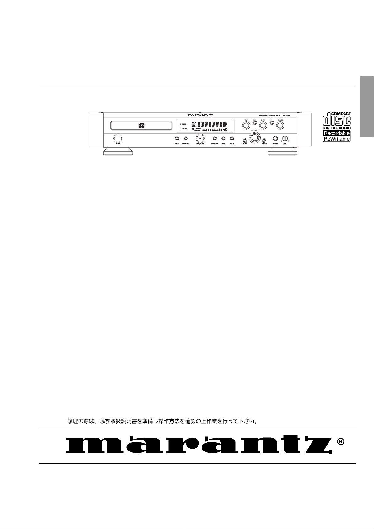
Compact Disc Recorder
DR-17
TABLE OF CONTENTS
Please use this service manual with referring to the user guide (D.F.U) without fail.
Printed in Japan
2. CDRL3610/10 (CDR MODULE for MARANTZ )
2.1 BLOCK DIAGRAM MAIN BOARD ......................................................................2-1
2.2 PARTS LOCATION.............................................................................................2-3
2.3 EXPLODED VIEW AND PARTS LIST ................................................................2-7
- DR-17 -
376K855010 AO
3120 785 00030
First Issue:1999.07
Page 2
MARANTZ DESIGN AND SERVICE
Using superior design and selected high grade components, MARANTZ company has created the ultimate in stereo sound.
Only original
it is famous.
Parts for your
ORDERING PARTS :
Parts can be ordered either by mail or by Fax.. In both cases, the correct part number has to be specified.
The following information must be supplied to eliminate delays in processing your order :
1. Complete address
2. Complete part numbers and quantities required
3. Description of parts
4. Model number for which part is required
5. Way of shipment
6. Signature : any order form or Fax. must be signed, otherwise such part order will be considered as null and void.
MARANTZ parts can insure that your MARANTZ product will continue to perform to the specifications for which
MARANTZ equipment are generally available to our National Marantz Subsidiary or Agent.
USA
MARANTZ AMERICA, INCMARANTZ AMERICA, INC.
440 MEDINAH ROAD
ROSELLE, ILLINOIS 60172
USA
PHONE : 630 - 307 - 3100
FAX : 630 - 307 - 2687
SUPERSCOPE TECHNOLOGIES, INC.
MARANTZ PROFESSIONAL PRODUCTS
2640 WHITE OAK CIRCLE, SUITE A
AURORA, ILLINOIS 60504 USA
PHONE : 630 - 820 - 4800
FAX : 630 - 820 - 8103
AMERICAS
AUSTRALIA
SCAN AUDIO PTY. LTD.
52 CROWN STREET, RICHMOND 3121
VICTORIA
AUSTRALIA
PHONE : +61 - 3 - 9429 - 2199
FAX : +61 - 3 - 9429 - 9309
NEW ZEALAND
SCAN AUDIO PTY. LTD.
8C PIERMARK DRIVE, ALBANY.
NORTH SHORE, AUCKLAND.
NEW ZEALAND
PHONE : +64 - 9444 - 4710
FAX : +64 - 9444 - 1346
EUROPE / TRADING
MARANTZ EUROPE B.V.
P.O.BOX 80002, BUILDING SFF2
5600 JB EINDHOVEN
THE NETHERLANDS
PHONE : +31 - 40 - 2732241
FAX : +31 - 40 - 2735578
CANADA
LENBROOK INDUSTRIES LIMITED
633 GRANITE COURT,
PICKERING, ONTARIO L1W 3K1
CANADA
PHONE : 905 - 831 - 6333
FAX : 905 - 831 - 6936
THAILAND
MRZ STANDARD CO.,LTD
746 - 754 MAHACHAI ROAD.,
WANGBURAPAPIROM, PHRANAKORN,
BANGKOK, 10200 THAILAND
PHONE : +66 - 2 - 222 9181
FAX : +66 - 2 - 224 6795
TAIWAN
PAI- YUING CO., LTD.
6 TH FL NO, 148 SUNG KIANG ROAD,
TAIPEI, 10429, TAIWAN R.O.C.
PHONE : +886 - 2 - 25221304
FAX : +886 - 2 - 25630415
BRAZIL
MARANTZ BRAZIL
CAIXA POSTAL 21462
CEP 04698-970
SAO PAULO, SP, BRAZIL
PHONE : 0800 - 123123
FAX : +55 11 534. 8988
(Discagem Direta Gratuita)
SINGAPORE
WO KEE HONG (S) PTE LTD
WO KEE HONG CENTRE
NO.23, LORONG 8, TOA PAYOH
SINGAPORE 319257
PHONE : +65 2544555
FAX : +65 2502213
MALAYSIA
WO KEE HONG ELECTRONICS SDN. BHD.
NO. 102 JALAN SS 21/35, DAMANSARA
UTAMA, 47400 PETALING JAYA
SELANGOR DARUL EHSAN, MALAYSIA
PHONE : +60 3 - 7184666
FAX : +60 3 - 7173828
JAPAN
Technical
MARANTZ JAPAN, INC.
35- 1, 7- CHOME, SAGAMIONO
SAGAMIHARA - SHI, KANAGAWA
JAPAN 228-8505
PHONE : +81 42 748 1013
FAX : +81 42 748 9190
KOREA
MK ENTERPRISES LTD.
ROOM 604/605, ELECTRO-OFFICETEL, 16-58,
3GA, HANGANG-RO, YONGSAN-KU, SEOUL
KOREA
PHONE : +822 - 3232 - 155
FAX : +822 - 3232 - 154
SHOCK, FIRE HAZARD SERVICE TEST :
CAUTION : After servicing this appliance and prior to returning to customer, measure the resistance between either primary AC
cord connector pins ( with unit NOT connected to AC mains and its Power switch ON ), and the face or Front Panel of product and
controls and chassis bottom.
Any resistance measurement less than 1 Megohms should cause unit to be repaired or corrected before AC power is applied, and
verified before it is return to the user/customer.
Ref. UL Standard No. 1492.
In case of difficulties, do not hesitate to contact the Technical
Department at above mentioned address.
990521A.O
Page 3
Servicing the DR-17
1. INTRODUCTION:
The DR-17 is the consumer version of a CD recorder, this means that the SCMS (Serial Copy Management System) is
included. The DR-17 can only record on the Audio CDRs (Consumer Use).
The DR-17 is suitable for recording and playback of CD-RW discs (CD-Re Writable disc).
Playback & Recording and Disc
Disc
Player/Recorder
Audio CD Player
Current products Ex:CD-17
Audio CD Player
CD-RW playback Ex:CD-17MK II
CD-RW Recorder
For Professional Ex:CDR630/640
CD-RW Recorder
For Consumer Ex:DR-17
CDR
CD
Consumer Disc
Finalized
non
Finalized
Professional Disc
Finalized Finalized
non
Finalized
Consumer Disc
Finalized
PP no P no no no no no -
PP no P no P no P no -
P P P/R P P/R P/R P/R P/R P/R no
P P P/R P no P/R P/R no no YES
CD-RW
non
Finalized
Professional Disc
non
Finalized
SCMS
Consumer : For Digital Audio
Professional : For General use (Including PC)
P : Playback
R : Recording
2. OPENING THE PRODUCT:
The product can be opened by removing the top cover (8 screws). Once the product is opened one can have access to the
several PCB’s and the main module. To have access to the Display PCB, the Headphone PCB and the lever PCB first the
front cover has to be removed (See dismantling instructions on page1-7).
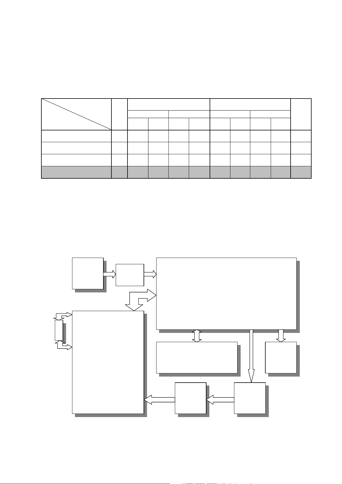
POWER
SW
BOARD
Trans-
former
POWER SUPPPLY
and
AUDIO
BOARD
MOTER
BOARD
CDR LOADER
DISPLAY BOARD
(CDL3610/01)
LEVEL
BOARD
Below the several PCB’s and it function and service policy will be discussed:
1-1
HEAD
PHONE
BOARD
ANALOG
INPUT
BOARD
Page 4

2.1 CDR loader (CDR main module CDL3610/01):
This complete CDR loader is considered as not repairable in the field. therefore this module will be repaired centrally. A
module exchange procedure will be set up for this purpose. The module can be removed from the product by removing 10
screws and the transformer (see demounting the CDR module on page 1-7), and loosing the connectors.
This module is the complete CD recorder, it contains the following parts:
`` CD Mechanism (CDM3610’). Underneath this mechanism a PCB is mounted which is adjusted to the mechanism (laser
current settings are stored in EEPROM).
`` Loader Assy. This mechanical assy takes care for the tray control.
`` Main PCB. This PCB takes care that the (analog or digital) signal to be recorded is converted into a suitable signal which
can be recorded on the disc.
Digital signals with an other sampling frequency then 44.1kHz will be converted in the sample rate converter (GDIN) to
44.1kHz.
Analog signals will be first converted into a digital converter by the AD converter.
This PCB also takes care that the signal from the CD (playback) is converted into a suitable digital signal (or analog via
the DA converter).
The main microprocessor controls the several functions of this PCB. The system software stored in a normal DIL
EPROM(7322). This EPROM(7322) is mounted on a socket, so software updates can be easily done at the dealer or
service agent.
2.2 Power SW Board.
This PCB contains the Power SW, which is jointed the Power bottom on the front panel. All parts are available as spare
parts.
2.3 Power Supply and Audio Board.
This PCB consists of power supply part and audio part. The power suppluy part delivers the several voltages for the diffrent
PCB in the DR-17. On this power supply sevel fuses (secondary side) are mounted on this PCB. The audio part takes care
that the signal from CDR main module is converted into an analog signal via DA converter and outputs the analog signal.
This PCB contains the output and input connectors also. All parts are available as spare parts.
2.4 Display Board.
This PCB contains the Display, which informs the user about the status of the recording/playback process and it also takes
care for scanning the keys on the front panel. The information from the keys is fed via a I C connection to the main
microprocessor on the CDR loader module. Information which needs to be displayed is also fed via this I C line from the
main microprocessor on the CDR loader module to the display controller.
The parts for this PCB are available as service parts so this PCB can be repairable up to component level.
2
2
2.5 Headphone Board.
This PCB contains the headphone socket and potentiometer which controls the headphone volume. All parts are available
as spare parts.
2.6 Analog Input Board
This PCB contains the analog input (RCA) connector. All parts are available as spare parts.
2.7 Level Board.
This PCB contains the potentiometer to adjust the level of the analogue input signal. All parts are available as spare parts.
2.8 Moter Board.
This PCB takes care for the tray speed control. All parts are available as spare parts.
1-2
Page 5

3. TEST PROGRAMS.
The DR-17 has two built in test programs. These are the “Dealer Diagnostics” and the “Service Diagnostics”. Both
diagnostics can be used to determine which board or module is defect.
3.1 Dealer Diagnostics.
This test diagnostics the communication between the several ICs in the CDR module. To start the test press the buttons
<PLAY>+<STOP> simultaneously and switch on the power.
During this diagnostics the message “BUSY” is blinking on the display (this can last for a couple of minutes). When an error
is detected the message “ERROR” is displayed. For the meaning of this error the service diagnostics has to be ran.
Since no CD is used for this test, the playback and record parts of the module are not tested thoroughly.
3.2 Service Diagnostics.
This Diagnostics tests the main board and CDM assembly (also known as Basic Engine) of the CDR module and the
keyboard and display board.
If an error is detected, an error number is displayed which refers to the error.
The test is executed with a normal CD loaded, so the recording part of the CDM is not tested thoroughly.
To start the test press the keys <PLAY>+<NEXT> simultaneously and switch the power on.
See the attached sheet for a flowchart of the “SERVICE TEST PROGRAM”.
1-3
Page 6

1.1 TECHNICAL SPECIFICATIONS
General
System .............................................................................................................................. compact disc digital audio
Number of channels....................................................................................................................................2 (stereo)
Applicable discs .............................................................................. CD, CD-R (digital audio), CD-RW (digital audio)
Power supply .................................................................................................................... AC 230 V (DR-17/N1G,B)
AC 120 V (DR-17/U1G,B)
AC 100 V (DR-17/FIN)
Power consumption ........................................................................................................................................... 25 W
Operating temperature..................................................................................................................................5 - 35
Weight ...............................................................................................................................................................8.0 kg
Dimensions ............................................................................................................ 458 (W) x 324 (D) x 83 (H) x mm
Audio
Frequency response ...........................................................................................................................20 Hz - 20 kHz
Playback S/N................................................................................................................................................... 105 dB
Playback dynamic range ...................................................................................................................................98 dB
Playback total harmonic distortion .................................................................................................................... 90 dB
Recording S/N................................................................................................................................................... 90 dB
Recording dynamic range ................................................................................................................................. 95 dB
Recording total harmonic distortion .................................................................................................................. 85 dB
Line output voltage
General CD .................................................................................................................................................. 2 Vrms
CD with HDCD ............................................................................................................................................. 4 Vrms
Digital coaxial output ........................................................................................................................... 0.5 V(pp)/75
Digital optical output...................................................................................................................................... -20 dBm
Headphones............................................................................................................................. 0 - 5 Vrms/8 - 2000
Recording values for line input/output
Digital coaxial input .................................................................................................................................. 32 - 48 kHz
(automatic sample rate conversion)
Digital optical input...................................................................................................................................32 - 48 kHz
(automatic sample rate conversion)
Analogue input Cinch .....................................................................................................................500 mVrms/50 k
Accessories
Remote control (+ batteries)
Audio cable (x 2)
Digital cable
coaxial cable (x 1) (DR-17/N1G,B • DR-17/U1G,B)
Fiber-optic cable (x 1) (DR-17/FIN)
Remote control cable (x 1)
AC power cord
1-4
Page 7
WARNING
All ICs and many other semiconductors are susceptible to
electrostatic discharges (ESD). Careless handling during
repair can reduce life drastically.
When repairing, make sure that you are connected with the
same potential as the mass of the set via a wristband with
resistance. Keep components and tools at this potential.
ATTENTION
Tous les IC et beaucoup d´autres semi-conducteurs sont
sensibles aux décharges statiques (ESD). Leur longévite
pourrait être considérablement écourtée par le fait qu´aucune
précaution nést prise à leur manipulation.
Lors de réparations, s´assurer de bien être relié au même
potentiel que la masse de l´appareil et enfileer le bracelet
serti d´une résistance de sécurité.
Veiller à ce que les composants ainsi que les outils que l´on
utilise soient également à ce potentiel.
WARNUNG
Alle ICs und viele andere Halbleiter sind empfindlich
gegenüber elektrostatischen Entladungen (ESD).
Unsorgfältige Behandlung im Reparaturfall kann die
Lebensdauer drastisch reduzieren.
Sorgen Sie dafür, daß sie im Reparaturfall über ein Pulsarmband mit Widerstand mit dem Massepotential des
Gerätes verbunden sind.
Halten Sie Bauteile und Hilfsmittel ebenfalls auf diesem
Potential.
WAARSCHUWING
Alle IC´s en vele andere halfgeleiders zijn gevoelig voor
electrostatische ontladingen (ESD).
Onzorgvuldig behandelen tijdens reparatie kan de levensduur
drastisch doen vermindern. Zorg ervoor dat u tijdens reparatie
via een polsband met weerstand verbonden bent met hetzelfde
potentiaal als de massa van het apparaat.
Houd componenten en hulpmiddelen ook op ditzelfde potentiaal.
AVVERTIMENTO
Tutti IC e parecchi semi-conduttori sono sensibili alle scariche
statiche (ESD).
La loro longevità potrebbe essere fortemente ridatta in caso di
non osservazione della più grande cauzione alla loro
manipolazione. Durante le riparationi occorre quindi essere
collegato allo stesso potenziale che quello della massa
delápparecchio tramite un braccialetto a resistenza.
Assicurarsi che i componenti e anche gli utensili con quali si
lavora siano anche a questo potenziale.
Safety regulations require that the set be restored to its
original condition and that parts which are identical with
those specified be used.
Safety components are marked by the symbol
Le norme di sicurezza estigono che l´apparecchio venga
rimesso nelle condizioni originali e che siano utilizzati i
pezzi di ricambiago identici a quelli specificati.
Componenty di sicurezza sono marcati con
Veiligheidsbepalingen vereisen, dat het apparaat in zijn
oorspronkeliijke toestand wordt teruggebracht en dat
onderdelen, identiek aan de gespecificeerde, worden toegepast.
De Veiligheidsonderdelen zijn aangeduid met het symbool
Varning !
Osynlig laserstrålning när apparaten är öppnad och
spärren är urkopplad. Betrakta ej strålen.
Advarsel !
Usynlig laserstråling ved åbning når sikkerhedsafbrydere
er ude af funktion. Undgå udsaettelse for stråling.
Varoitus !
Avatussa laitteessa ja suojalukituksen ohitettaessa olet alttiina
näkymättömälle laserisäteilylle. Älä katso säteeseen !
ESD
SAFETY
Bei jeder Reparatur sind die geltenden Sicherheitsvorschriften zu beachten. Der Originalzustand des Gerätes
darf nicht verändert werden. Für Reparaturen sind Originalersatzteile zu verwenden.
Sicherheitsbauteile sind durch das Symbol markiert.
Les normes de sécurité exigent que l`appareil soit remis
à l`état d`origine et que soient utilisées les pièces de
rechange identiques à celles spécifiées.
Les composants de sécurité sont marqués
LASER PRODUCT
CLASS 3B
U : VERSION N : VERSION
LASER PRODUCT
DANGER: Invisible laser radiation when open.
"Pour votre sécurite, ces documents doivent être utilisés par
des spécialistes agréés, seuls habilités à réparer votre
appareil en panne".
After servicing and before returning the set to customer
perform a leakage current measurement test from all
exposed metal parts to earth ground, to assure no
shock hazard exists.
The leakage current must not exceed 0.5mA.
AVOID DIRECT EXPOSURE TO BEAM.
AVAILABLE ESD PROTECTION EQUIPMENT :
anti-static table mat large 1200x650x1.25mm 4822 466 10953
small 600x650x1.25mm 4822 466 10958
anti-static wristband 4822 395 10223
connection box (3 press stud connections, 1M ) 4822 320 11307
extendible cable (2m, 2M , to connect wristband to connection box) 4822 320 11305
connecting cable (3m, 2M , to connect table mat to connection box) 4822 320 11306
earth cable (1M , to connect any product to mat or to connection box) 4822 320 11308
KIT ESD3 (combining all 6 prior products - small table mat) 4822 310 10671
wristband tester 4822 344 13999
1.2 WARNINGS
CLASS III b
1-5
Page 8
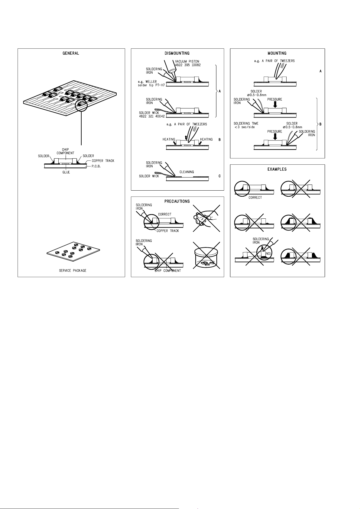
1.3 SERVICE HINTS
SERVICE TOOLS
Audio signals disc 4822 397 30184
Disc without errors (SBC444)+
Disc with DO errors, black spots and fingerprints (SBC444A) 4822 397 30245
Disc (65 min 1kHz) without no pause 4822 397 30155
Max. diameter disc (58.0 mm) 4822 397 60141
Torx screwdrivers
Set (straigh) 4822 395 50145
Set (square) 4822 395 50132
13th order filter 4822 395 30204
Hexagon socket screw button (No. 1.5)
1-6
Page 9
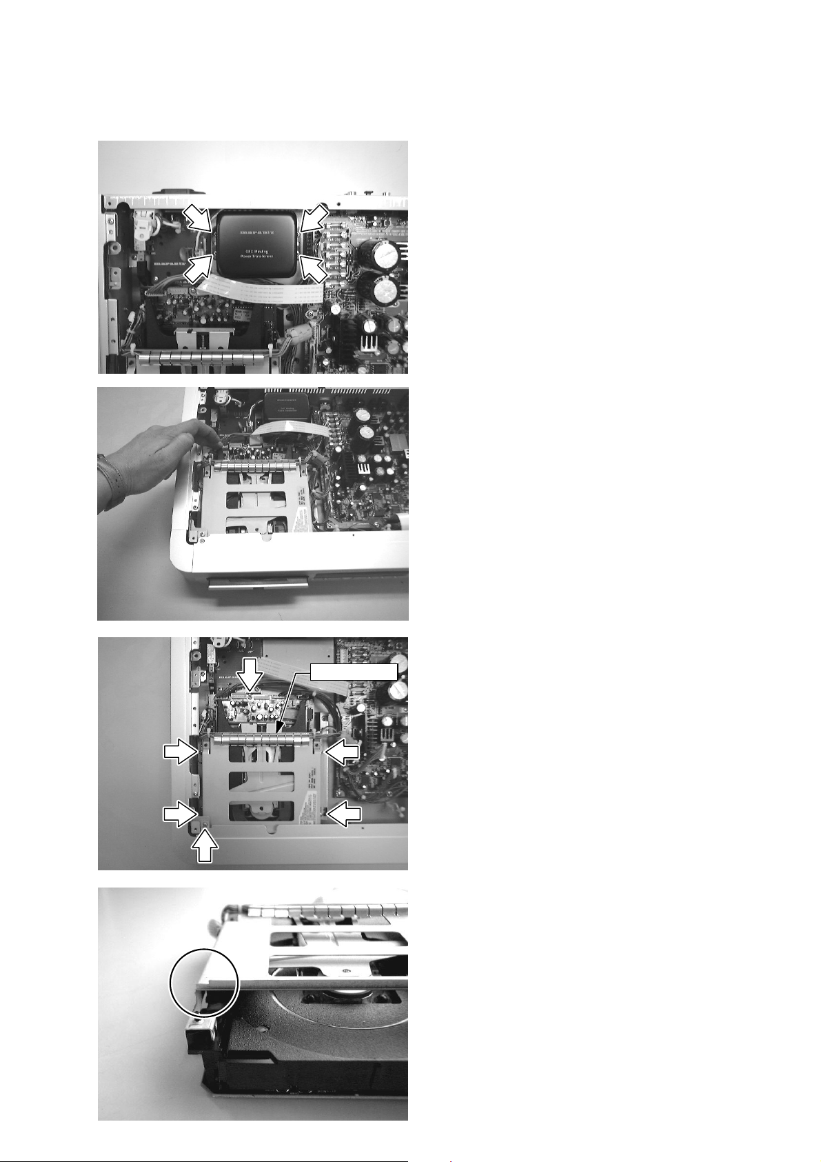
1.4 DISMOUNTING INSTRUCTION
1. DISMOUNTING CDR LODER
4
1
1) Remove 8 screws (002D & 003D) from the top cover .
2) Remove the top cover (001D).
3) Disconnect connector cables from J801 and JH04.
4) Remove 4 screws (1-4), and remove the mains transformer (L001).
3
5
2
Cable Shield
5) Come out (Open) the CD tray by manually.
6) Remove the CD tray lid (050B+052B+062B).
7) Remove screw (5) from the bracket (004B).
8) Remove 4 screws (6-10).
9) Disconnect all cables from connectors (JF02, 1330,
1410, 1400, 1430 and 1440).
10
6
9
8
7
10) Disconnect cables from connectors (J891 and J892),
and remove PCB P816.
11) Connect the cables from “TRAY MOTOR” to the con-
nector 1104.
12) Remove the cable shield (003X) from the top frame
REMARK: When replace the CDR loader module
CDRL3610’ to the new one. It is necessary to cut left
side of the top frame by the hand nibbler.
(Height 2mm x Width 6mm)
1-7
Page 10
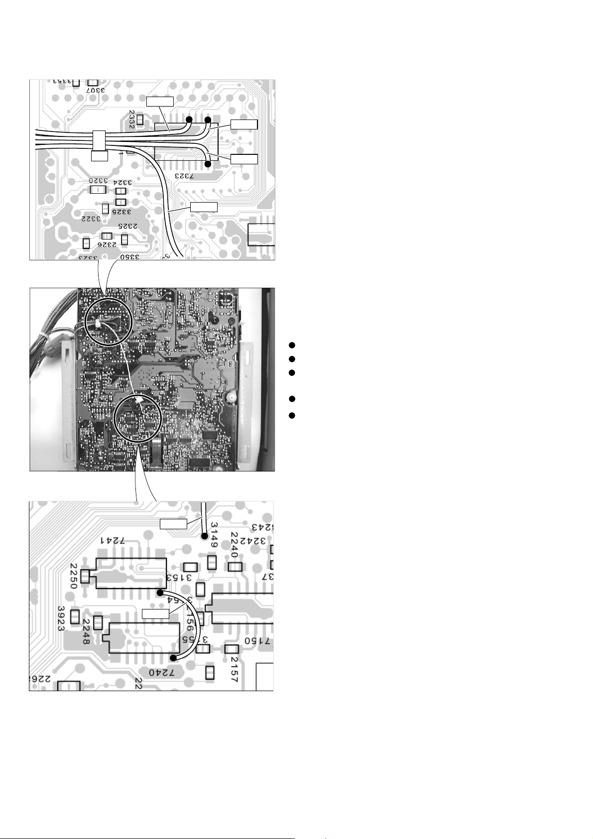
2. DISMOUNTING ADDITIONAL CABLES
ORG
EYL
De-soldering and remove cables from the loader PCB.
RED
BRN
REMARK: When replace the CDR loader module
CDRL3610’ to the new one. It is necessary to add
removed cables at same positions as follows;
BROWM ............ Pin 9 of IC7323
RED................... Pin 12 of IC7323
ORANGE........... Pin 15 of IC7323
BLK
YELLOW ........... Test Point beside 3149
BLACK............... Pin 7 of IC7240 and Pin 7 of IC7241
EYL
1-8
Page 11
HDCD Technology
HDCD® and High Definition Compatible Digital®
are registered trademarks of Pacific Microsonics, Inc
HDCD
1
2
28
19 5 27 18
4121110
25
26
24
23
20
16 17 15
14
13
6
3
9
HDCD - High Definition Compatible Digital - is a patented process for delivering on digital media the full richness and detail of
the original microphone feed. When listening to HDCD recordings, you will hear more dynamic range and very natural vocal
and musical timbre. With HDCD, you get the body, depth and emotion of the original performance - not a flat, digital image.
HDCD encoded CDs sound better because they are encoded with 20 bits of real music information, compared to 16 bits for all
other CDs. HDCD overcomes the limitations of the 16-bit CD format by using a sophisticated system to encode the additional
the CD format.
In addition, HDCD Precision Digital Filtering has the benefit of improving the sound of all digital recordings. This means that the
Marantz DR-17, equipped with HDCD, will improve the sound of all digital recordings, whether mastered with HDCD or not.
1-9
Page 12
S
EC.
PRI .
VOLTAGE FAILLING
DETECT
MUTING
CONTROL
POWE R SUPPL Y
VOLTAGE REGULATOR
+12Va +5Va -5Va -12Va +12Vd +8V +5Vd +5Vm -8Vd-26V
+/- 12Va
+/- 5Va
+12Vd
+5Vd /+5Vm
+/-8Vd
-26V
DC1/DC2
L001
POWE R IN PUT
VY01
ZY01
KEYS
uCOM
HDCD
PLAY, STOP, REC, etc
MUTING
CKT
HDAM
HDAM
BITSTREAM
DUAL DAC
QD01 TD A1547
KILL
DE-EMPHASIS
CKT
EMP
BITSTREAM
CONV ERSION
Q510 SAA7350
DOL
CLK
DOR
L.CH
R.CH
HDCD PROCESS
DECORDER
AND
Q501 PMD-100
OVER SA MPL IN G
FS x8
SD1
SD2
SCK
WS
DIGITAL AUDI O
INPUT/OUTPUT
Q501 TDA1315H
LRCK
BCK
DATA
Q601
Q602
FIL T ER
FIL T ER
DIG.COAX
LT01
DIG.OPT
OUTPU T
OUTPUT
DIG.COAX
DIG.OPT
INPUT
INPUT
RC-BU S
INPUT
RC-BU S
OUTPU T
BUS REC
CONTROL
CD_SYNC
DETECT DISPLAY DRIVER, KEY SENS, IR SENS
XY01
8MHz
40 SY SCL K O
384FS
INT
ENT
SF01
J902
HPL
HPR
HPR
HPL
L.CH
R.CH
Q701+R721+Q721
Q701+R721+Q721
CDL 3610
KEY SENS BUS
DISPLAY
CONTROL BUS
CONTROL BU S
CDR M ODUL E
DIGOU T
SRC
SRC O N
DETECT
LPWR
PLAY/REC
DAIO_REC
UNLOCK_GDIN
DIGIN
OPTIN
LEFTINOUT
RIGH TINOU T
RSTLA, I NTERRUPT
SCL , SD A
P1- P16
G1-G13
KSCAN1-3
KSENS1-5
INT1, IR
HDCD 27
FORMA T
TRANS-
FORMA TI ON
6 IECI N0
353736
1282
262523
24
789
10
424344 3
5,28
30
14
15
18
19
6 XTI 14 XIN
R910+Q901
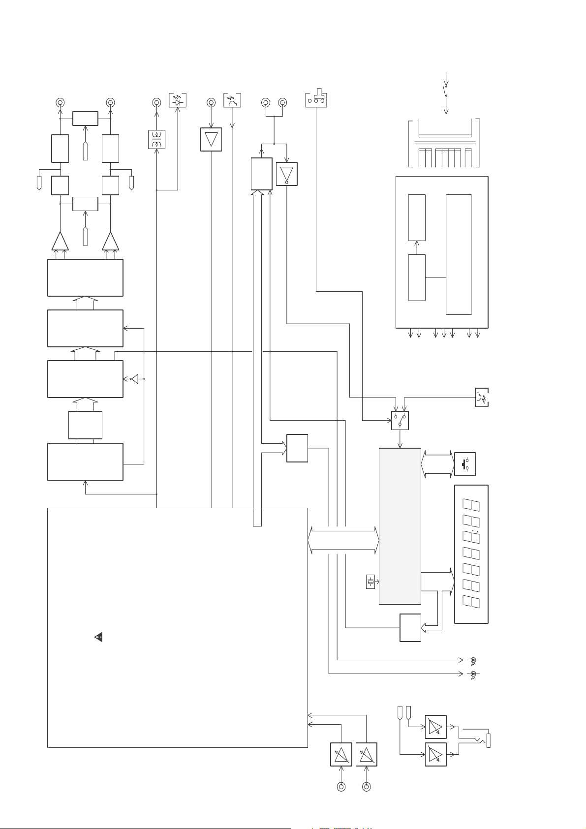
1.5 BLOCK DIAGRAM
1-10
Page 13
USER
MICRO
TTL
7481
7300
?
IIS
SPI
CRIN
33MHz
DAC
TDA1305T
7440
7480
I2C-BUS
SCL
SDA
7323
7322
7321
2
GDIN
DAI-O
ADC
SRAM
ROM
EXP
TDA1373H/N2
TDA1315
SAA7366
7465
7405
7192,7193,7195
7182,7183,7185
TRAY MOTOR CONTROL
PROCESSING
WOBBLE
WOBBLE
EFM
MOTO1/2
MPWM
TRAY SENSE
TRAYMOTOR
SERVO
CDM-36
LASER
PHOTO
DIODES
FOCUS
RADIAL
SLEDGE
MOTOR
DISC
CDM BOARD
MOTOR BOARD
& TIMING
CONTROL
LASER
AEGER
PROCESSOR
SIGNAL
MAIN BOARD
32MHz
MICRO
CONTROLLER
CDCEP
CD-ENCODER
CD-DECODER
DSICR
CONTROLLER
SERVO
DRIVER
SERVO
DIGITAL
16MHz
68HC11K4
CONTROLLER
7170
1177
7320
7245
7210
7130
7105
C1-4
S1/S2
ANALOG
7010
DAC
7016
EEPROM
7014
LOADER ASSY
7150 - 7230 - 7235
PPN
CA/HFM
REN
TLN
FEN
MIRN
DIGITAL
UVW
UVW
7280 7297
7270
NEC 784036
CDE
TDA1371
CD60
LO9585P
CLO3
CLO1
CDR LOADER
1-11
Page 14
y
y
y
1.6 SERVICE TEST PROGRAM
If power ON,
switch power OFF
DEALER DIAGNOSTICS
(status of player)
<PLAY> + <STOP>
Press
simultaneously and switch
power on
Display shows blinking:
“BUSY”
during the test.
no
Set OK?
es
set displays:
“
PASSED
to end test, switch power off
”
set displays:
“ERROR”
ELECTRICAL SERVICE
DIAGNOSTICS
(advice for replacement units)
Load CDDA disc(SBC444A)
<PLAY> + <NEXT>
Press
simultaneously and switch
power on
MAIN BOARD TEST
Display shows blinking
“D -----”
BASIC ENGINE TEST
Display shows
during the test
no
Test OK?
es
“B -----”
during the test
set displays:
“DERR n”
n
=
1 : RAM test error
2 : ROM test error
3 : EEPROM test error
4 : DAIO test error
5 : GDIN test error
NEXT
<
(erasement of complete disc)
mm
ss
TOTAL
illuminated
DC ERASE
Load CD-RW disc
<ERASE> + <RECORD>
simultaneously and switch
during the erase function.
when the erase function is
Press
power on
Display shows:
“
ER mm:ss
:remaining minutes
:remaining seconds
REM
and
Display shows:
“
PASSED
completed.
>
switch power off.
”
are also
”
no
Test OK?
es
DISPLAY TEST
All segments are blinking at a
frequency of 1Hz.
NEXT
<
KEYBOARD/REMOTE TEST
Display shows name of
pressed key on keyboard or
remote control.
To end test, switch power off.
set displays:
“BERR n”
n
=
1 : Communication bus error
2 : Basic Engine self test error
3 : Disc test error
NEXT
<
>
>
1-12
Page 15

1.7 FAULTFINDING GUIDE
NO DISC
POWER ON
CHECK:
POWER SUPPLY
DISC
DETECTION
STARTS?
YES
DISPLAY?
YES
NO
DISPLAY
NO
MAINS SWITCH SH01
FUSES
MAINS TRANSFORMER
VOLTAGES AC, DC, FTD
WIRING
POWER SUPPLY VOLTAGES
CLOCK FREQUENCY 8MHz
CONTROL LINES
WIRING
ELECTRICAL SERVICE DIAGNOSTICS:
DISPLAY TEST
SEE MEASUREMENTS DISPLAY
DISPLAY
SHOWS
NO DISC
“
YES
OPEN/CLOSE
YES
LOAD DISC
PRESS OPEN/CLOSE
”?
PRESS
TRAY?
DISPLAY SHOWS BLINKING “
CHECK:
NO
NO
POWER SUPPLY VOLTAGES -12V, -8V
ELECTRICAL SERVICE DIAGNOSTICS:
REPLACE CDR MODULE IF ERROR OCCURS
CHECK:
ELECTRICAL SERVICE DIAGNOSTICS:
KEYBOARD TEST: OPEN/CLOSE SWITCH ON
DISPLAY BOARD.
IF OK, REPLACE CDR MODULE
SERVICE”
CDDA DISC?
SEE CDDA DISC
FAULTFINDING
CD-R DISC?
YESYES
SEE CD-R DISC
FAULTFINDING
NONO
SEE CD-RW DISC
FAULTFINDING
1-13
Page 16

CDDA DISC FAULTFINDING GUIDE
CDDA DISC LOADED
DISPLAY SHOWS:
“CD”
T.O.C. INFO
YES
PRESS PLAY
AUDIO?
YES
NO
SERVICE TEST MODE:
ELECTRICAL SERVICE DIAGNOSTICS:
REPLACE CDR MODULE IF ERROR OCCURS.
CHECK:CONNECTOR BOARD
FLEX CONNECTION TO CDR MODULE
NO
PLAY AUDIO SIGNALS DISC TRACK 15:
SIGNAL OF 5.4 VPP ON PINS 1 AND 5 OF CONN.
JT03
KILL VOLTAGE ON PIN 7 OF CONN. JT03:
-8V DURING PLAY, +5V DURING STOP, PAUSE?
KILL TRANSISTORS QN51, QN52, QN53, QN54,
DISTORTION?
NO
HEADPHONE?
YES
DIGITAL OUT?
OPTICAL OUT?
YES
YES
NO
NO
NO
SERVICE TEST MODE:
ELECTRICAL SERVICE DIAGNOSTICS:
REPLACE CDR MODULE IF ERROR OCCURS.
CHECK:HEADPHONE BOARD
WIRING
OP-AMP Q901
KILL TRANSISTORS QN91, QN92
CHECK:POWER SUPPLY AND AUDIO BOARD
FLEX CONNECTION TO CDR MODULE
DIGITAL OUT TRANSFORMER LT04
IC QT01
CHECK:CONNECTOR BOARD
OPTICAL TRANSMITTER JT02
SAFETY RESISTOR 3501
IC QT01
PLAY BACK OF CDDA
DISCS OK
1-14
Page 17

CD-R DISC FAULTFINDING
CD-R DISC LOADED
DISPLAY SHOWS:
CD” “RECORDABLE”
“
“OPC”
T.O.C. INFO
YES
CD-R DISC PARTIALLY
RECORDED OR EMPTY.
START RECORDING
FROM ANALOGUE
SOURCE
LEVEL
ADJUSTABLE?
YES
START RECORDING
FROM DIGITAL
SOURCE
NO
NO
DISPLAY SHOWS:
CD” “RECORDABLE”
“
T.O.C. INFO
YES
FINALISED CD-R DISC
LOADED.
CHECK LEVEL BOARD:
WIRING
POTMETER R721
OP-AMP Q721
NO
ELECTRICAL SERVICE
DIAGNOSTICS: REPLACE CDR
MODULE IF ERROR
DIGITAL IN?
OPTICAL IN?
YES
RECORDING
SUCCESSFUL?
YES
SET OK
NO
CHECK CONNECTOR BOARD:
FLEX CONNECTION
IC Q311
RECEIVER J301
NO
ELECTRICAL SERVICE
DIAGNOSTICS: REPLACE CDR
MODULE IF ERROR
1-15
Page 18

CD-RW DISC FAULTFINDING
CD-RW DISC LOADED
DISPLAY SHOWS:
CD” “REWRITABLE”
“
“OPC”
T.O.C. INFO
YES
CD-RW DISC PARTIALLY
RECORDED OR EMPTY
START ERASING
ERASING
SUCCESSFUL?
YES
SET OK
NO
DISPLAY SHOWS:
CD” “REWRITABLE”
“
T.O.C INFO
YES
FINALISED CD-RW
LOADED
NO
SERVICE TEST PROGRAM:
ELECTRICAL SERVICE DIAGNOSTICS
IF DISC CORRUPTED, TRY DC ERASE
NO
SERVICE TEST PROGRAM
ELECTRICAL SERVICE
DIAGNOSTICS: REPLACE CDR
MODULE IF ERROR
1-16
Page 19

MEASUREMENTS DISPLAY PANEL
Measurement of voltage supplies.
1.
Several voltages arrive at the display PCB.
Measurements and limits.
Voltage Nominal value Limits
VFTD -26V
VDC1-DC2 3.5V
5V+5Vd
Measurement of oscillator.
2.
5%
10%
5%
As clock driver for the display controller a resonator of 8MHz is used.
The clock frequency is available at pin 8 of the display controller.
Check the frequency of 8MHz
5%.
3. Checking the control lines.
There are several lines which are inputs to the display controller and others which are outputs,
these lines have to be checked to guarantee basic functionality.
RESETN:
This line should be kept low during power up for at least 3 machine cycles,with supply voltage
within the operating range and oscillation stable.1 machine cycle = 12 X 1/Fc (8Mhz) Sec.
SDA and SCL:
The level on these two lines must be checked. When there is no communication they should have
the `High' level.
INTERRUPT:
The interrupt line is an output for the display controller. Check if this level is high after reset, no key
pressed and no RC5 coming in.
Key matrix lines:
Check if at I/O port 4 of the controller all pins are high.(No keys pressed).(Pin 26 to 33). If not
check respective pull-up resistors.
4. Operation of grid and segment control lines.
+5V
-26V
PM3392A
ch1: max = 5.00
1
T
STOP
CH1 5.00 V= MTB 200us- 1.90dv
This figure shows the signal generated by the
display processor on one of the grid lines. The
level on the grid line changes from -26V to +5V.
The grid lines are scanned successively about every 950
sec.
1-17
Page 20

1.8 COMPONENT DESCRIPTIONS
Q301 : TDA1315H
SYMBOL PIN PADCELL DESCRIPTION
RC
fil
V
ref
V
DDA
V
SSA
IECIN1 5 E007 high sensitivity IEC input
IECIN0 6 IPP04 TTL level IEC input
IECSEL 7 IUP04 select IEC input 0 or 1 (0 = IECIN0; 1 = IECIN1); this input has an internal pull-up
IECO 8 OPFH3 digital audio output for optical and transformer link
IECOEN 9 IUP04 digital audio output enable (0 = enabled; 1 = disabled/3-state); this input has an
TESTB 10 IPP04 enable factory test input (0 = normal application; 1 = scan mode)
TESTC 11 IPP04 enable factory test input (0 = normal application; 1 = observation outputs)
UNLOCK 12 OPP41A PLL out-of-lock (0 = not locked; 1 = locked); this output can drive an LED
FS32 13 OPP41A indicates sample frequency = 32 kHz (active LOW); this output can drive an LED
FS44 14 OPP41A indicates sample frequency = 44.1 kHz (active LOW); this output can drive an LED
FS48 15 OPP41A indicates sample frequency = 48 kHz (active LOW); this output can drive an LED
CHMODE 16 OPP41A use of channel status block (0 = professional use; 1 = consumer use); this output
V
DDD2
V
SSD2
RESET 19 IDP09 initialization after power-on, requires only an external capacitor connected to V
PD 20 IPP04 enable power-down input in the standby mode (0 = normal application; 1 = standby
CTRLMODE 21 IUP04 select microcontroller/stand-alone mode (0 = microcontroller; 1 = stand-alone); this
LADDR 22 IPP04 microcontroller interface address switch input (0 = 000001; 1 = 000010)
LMODE 23 IPP09 microcontroller interface mode line input
LCLK 24 IPP09 microcontroller interface clock line input
LDATA 25 IOF24 microcontroller interface data line input/output
STROBE 26 IDP04 strobe for control register (active HIGH); this input has an internal pull-down resistor
UDAVAIL 27 OPF23 synchronization for output user data (0 = data available; 1 = no data)
TESTA 28 IPP04 enable factory (scan) test input (0 = normal application; 1 = test clock enable)
COPY 29 OPP41A copyright status bit (0 = copyright asserted; 1 = no copyright asserted); this output
INVALID 30 IOD24 validity of audio sample input/output (0 = valid sample; 1 = invalid sample); this pin
DEEM 31 OPF23 pre-emphasis output bit (0 = no pre-emphasis; 1 = pre-emphasis)
MUTE 32 IUP04 audio mute input (0 = permanent mute; 1 = mute on receive error); this pin has an
I2SSEL 33 IUP04 select auxiliary input or normal input in transmit mode
SDAUX 34 IPP04 auxiliary serial data input; I
SD 35 IOF24 serial audio data input/output; I
WS 36 IOF24 word select input/output; I
SCK 37 IOF29 serial audio clock input/output; I
2
SOEN 38 IUP04 serial audio output enable (0 = enabled; 1 = disabled/3-state); this input has an
I
SYSCLKI 39 IPP09 system clock input (transmit mode)
SYSCLKO 40 OPFA3 system clock output (receive mode)
V
SSD1
V
DDD1
CLKSEL 43 IUP04 select system clock (0 = 384f
RC
int
1 E029 PLL loop filter input
2 E029 decoupling internal reference voltage output
3 E008 analog supply voltage
4 E004 analog ground
resistor
internal pull-up resistor
can drive an LED
17 E008 digital supply voltage 2
18 E009 digital ground 2
this is a Schmitt-trigger input with an internal pull-down resistor
mode)
input has an internal pull-up resistor
can drive an LED
has an internal pull-down resistor
internal pull-up resistor
2
S-bus
2
S-bus
2
S-bus
2
S-bus
internal pull-up resistor
41 E009 digital ground 1
42 E008 digital supply voltage 1
; 1 = 256fs); this input has an internal pull-up resistor
s
44 E029 integrating capacitor output
DDD
;
1-18
Page 21

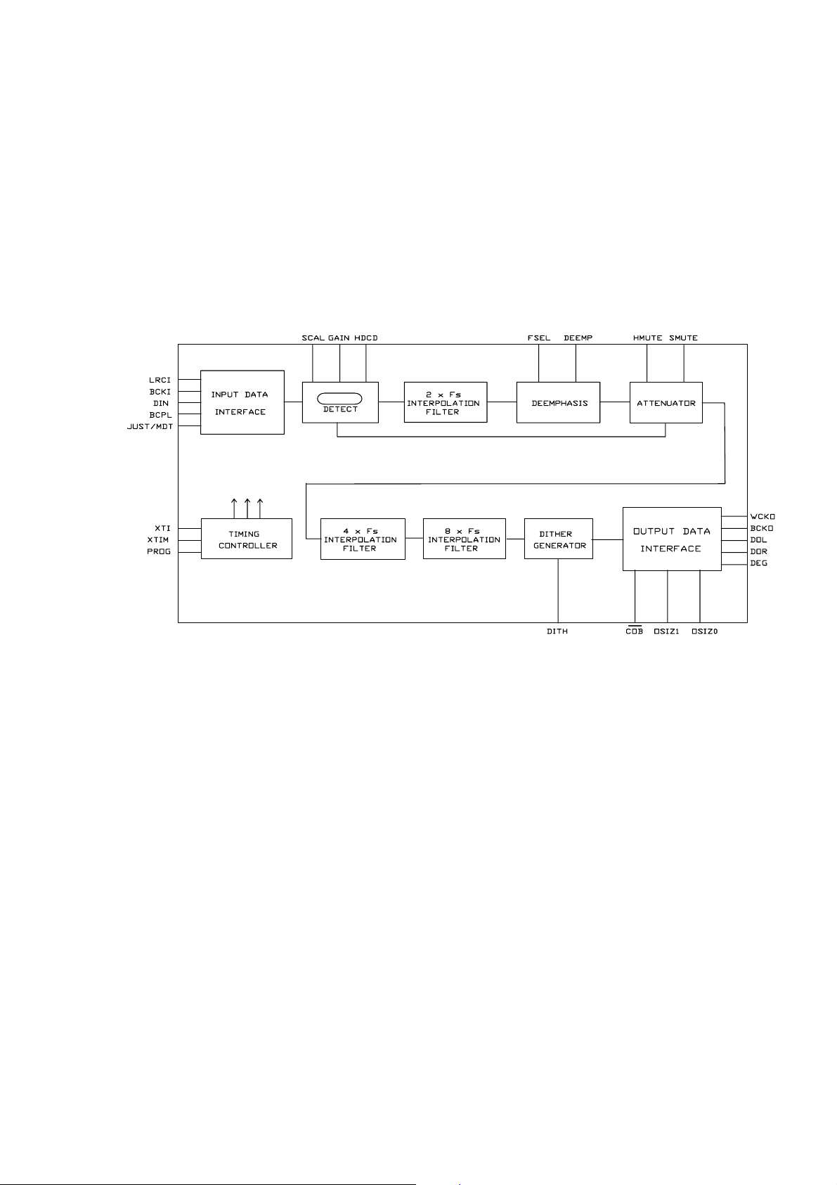
Q510 : PMD-100
PIN SYNBOL I/O FUNCTION
1 DIN I Serial data input
2 BCKI I Bit clock input
3 XTIM I Select system clock frequency
Low = 256fs, High = 384fs
4 DITH I Dither select
Low = dither disable, High = dither added
Analog output stage gain
5 GAIN O Use only if Pin 19 is High
Low = low gain, High = high gain (+6dB)
6 XTI I System clock input
7 VDD1 - +5 volt power for filter
8 VSS1 - Ground
9 PROG I Select program mode
Low = Stand-alone, High = Program
16 Bits 18Bits 20Bits 24Bits
10 OSIZ0 I 0101
11 OSIZ1 I 0011
Output data format
12 COB I Low = complementary offset binary
High = 2's complement
Input data justification
13 JUST I Low = data assumed tobe left justified up to 24 bits in length
High = data right justified 16 bits
Input datalatching
14 BCPL I Low = input data latched on rising edge of BCKI
High = input data latched on falling edge of BCKI
15 SMUTE I Soft mute Low = off, High = on
16 DEEMPH I De-emphasis filter Low = off, High = on
17 HMUTE I Hard mute Low = off, High = on
18 FSEL I De-emphasis filter Fs Low = 44.1kHz, High = 48kHz
Gain scaling
19 SCAL I Low = 6dB gain scaling is performed internally in the digital domain
High = Analog output gain stage is set jby pin 5 GAIN
20 DG O DAC sample and hold deglitch signal
21 VSS2 - Ground (Common with VSS1)
22 VDD2 - +5V volt puwer for output interface
23 DOR O Right channel serial data output
24 DOL O Left channle serial data output
25 WCKO O Word clock output
26 BCKO O Bit clock output
HDCD encoding detect
27 HDCD O Low = no encoding, High = HDCD encoding input data
(Output current ratad at 12mA)
28 LRCI I Word clock input
1-19
Page 22

QD01 : TDA1547
SYMBOL PIN DESCRIPTION
DGND 1 0 V digital supply
V
DDD
2 5 V digital supply for both channels
IN R 3 serial one-bit data input for the right channel
n.c. 4 pin not connected; should preferably be connected to digital ground
CLK R 5 clock input for the right channel
V
DDD R
6 5 V digital supply for the right channel; this voltage determines the internal logic HIGH level
in the right channel
V
SSD R
7 −3.5 V digital supply for the right channel; this voltage determines the internal logic LOW
level in the right channel
V
ref R
8 −4 V reference voltage for the right channel switched capacitor DAC
AGND DAC R 9 0 V reference voltage for the right channel switched capacitor DAC; this pin should be
connected to analog ground
−DAC R 10 output from the right negative switched capacitor DAC; feedback connection for the right
negative operational amplifier
+DAC R 11 output from the right positive switched capacitor DAC; feedback connection for the right
positive operational amplifier
AGND R 12 0 V reference voltage for both right channel operational amplifiers
n.c. 13 pin not connected; should preferably be connected to analog ground
+OUT R 14 + output of the switched capacitor operational amplifier
−OUT R 15 − output of the switched capacitor operational amplifier
V
V
SSA
DDA
16 −5 V analog supply
17 5 V analog supply
−OUT L 18 − output of the switched capacitor operational amplifier
+OUT L 19 + output of the switched capacitor operational amplifier
n.c. 20 pin not connected; should preferably be connected to analog ground
AGND L 21 0 V reference voltage for both left channel operational amplifiers
+DAC L 22 output from the left positive switched capacitor DAC; feedback connection for the left
positive operational amplifier
−DAC L 23 output from the left negative switched capacitor DAC; feedback connection for left negative
operational amplifier
AGND DAC L 24 0 V reference voltage for the left channel switched capacitor DAC; this pin should be
connected to analog ground
V
V
ref L
SSD L
25 −4 V reference voltage for the left channel switched capacitor DAC
26 −3.5 V digital supply for the left channel; this voltage determines the internal logic LOW level
in the left channel
V
DDD L
27 5 V digital supply for the left channel; this voltage determines the internal logic HIGH level in
the left channel
CLK L 28 clock input for the left channel
n.c. 29 pin not connected; should preferably be connected to digital ground
IN L 30 serial one-bit data input for the left channel
V
V
SSD
SUB
31 −5 V digital supply for both channels
32 −5 V substrate voltage
1-20
Page 23

QY01 : TMP87CH74F
PIN SYNBOL PORT NAME I/O FUNCTION
1 OPEN P02/SI1 2 OPEN P03 3 OPEN P04 4 OPEN P05 5 OPEN P06 6 OPEN P07 7 VSS1 VSS - Ground
8 XOUT XOUT O X'tal output
9 XIN XIN I X'tal input
10 RESETIN RESET I/O Reset input
11 OPEN P22/XOUT 12 OPEN P21/XINT 13 TEST1 TEST I Ground
14 OPEN P20/INT5/STOP 15 INT0 P10/INT0 I Interrupt
16 INT1 P11/INT1 I IR interrupt
17 OPEN P12/TC2/PPG 18 OPEN P13/DVO 19 OPEN P14/TC4/PDO/PWM 20 OPEN P15/INT3/TC1 21 OPEN P16/INT2 22 IR P17/INT4/TC3 I IR data input
23 SCL P30/SCL/SI0 I Serial clock input
24 SDA P31/SDA/SO0 I Serial data input
25 OPEN P32/SCK0 26 KSENS8 P40/AIN0 I Key sens
27 KSENS7 P41/AIN1 I Key sens
28 KSENS6 P42/AIN2 I Key sens
29 KSENS5 P43/AIN3 I Key sens
30 KSENS4 P44/AIN4 I Key sens
31 KSENS3 P45/AIN5 I Key sens
32 KSENS2 P46/AIN6 I Key sens
33 KSENS1 P47/AIN7 I Key sens
34 OPEN P50/AIN10 35 KSCAN3 P51/AIN11 O Key scan
36 KSCAN2 P52/AIN12 O Key scan
37 KSCAN1 P53/AIN13 O Key scan
38 VASS VASS - Ground
39 VAREF VAREF - +5V
40 VDD VDD - +5V
41 G13 P60/V0 O Grid output
42 G12 P61/V1 O Grid output
43 G11 P62/V2 O Grid output
44 G10 P63/V3 O Grid output
45 G9 P64/V4 O Grid output
46 G8 P65/V5 O Grid output
47 G7 P66/V6 O Grid output
48 G6 P67/V7 O Grid output
49 G5 P70/V8 O Grid output
50 G4 P71/V9 O Grid output
51 G3 P72/V10 O Grid output
52 G2 P73/V11 O Grid output
53 G1 P74/V12 O Grid output
54 OPEN P75/V13 55 OPEN P76/V14 56 OPEN P77/V15 57 P1 P80/V16 O Segment output
58 P2 P81/V17 O Segment output
59 P3 P82/V18 O Segment output
60 P4 P83/V19 O Segment output
61 P5 P84/V20 O Segment output
62 P6 P85/V21 O Segment output
63 P7 P86/V22 O Segment output
64 P8 P87/V23 O Segment output
65 P9 P90/V24 O Segment output
66 P10 P91/V25 O Segment output
67 P11 P92/V26 O Segment output
68 P12 P93/V27 O Segment output
69 P13 P94/V28 O Segment output
70 P14 P95/V29 O Segment output
71 P15 P96/V30 O Segment output
72 P16 P97/V31 O Segment output
73 OPEN PD0/V32 74 OPEN PD1/V33 75 OPEN PD2/V34 76 OPEN PD3/V35 77 OPEN PD4/V36 78 VKK VKK - Anode voltage for FTD
79 P0 P00/SCK1 I Ground
80 P1 P01/SI1 I Ground
QY01 : uPD6134
PIN SYNBOL PORT NAMEI/O FUNCTION
1 OPEN KIO06 2 OPEN KIO07 3 KSENS S0 I Key sens
4 RCOUT S1/LED O Data output
5 OPEN REM 6 VDD VDD - +2.7V
7 XOUT XOUT O Ground
8 XIN XIN I X'tal output
9 GND GND - X'tal input
10 RESET RESET I Reset input
11 OPEN KI0 12 OPEN KI1 13 OPEN KI2 14 OPEN KI3 15 OPEN KI/O0 16 OPEN KI/O1 17 OPEN KI/O2 18 OPEN KI/O3 19 KSCAN KI/O4 O Key scan
20 OPEN KI/O5 -
Q520 : ASS7550AGP
1-21
Page 24

1.9 WIRING DIAGRAM
LOADER BOARD
POWER TRANSFORMER
1290
1101
1102
1440
1430
1420
1400
1410
1330
1104
1103
1 SDA!
2 SCL!
3 RSTIN!
4 GROUND
5 Interrupt!
6 GROUND
7 VFTD!
8 DC2!
9 DC1!
10 GROUND
11 +5Vb!
1 LEFTFLEV!
2 GROUND
3 RIGHTFLEV!
4 -12Vb!
5 GROUND
6 +12Vb!
7 RIGHTTLEV!
8 GROUND
9 LEFTTLEV!
1 RIGHTOUT!
2 GROUND
3 GROUND
4 LEFTIN!
5 LEFTOUT!
6 GROUND
7 KILLBUF!
8 RIGHTIN!
9 +5Vb!
10 DIGIN!
11 GROUND
12 DIGOUT!
13 GROUND
14 OPTIN!
15 GROUND
16 GROUND
1 LEFTOUT!
2 GROUND
3 RIGHTOUT!
4 KILL!
5 -12Vb!
6 GROUND
7 +12Vb!
1 DC2!
2 DC1!
3 VFTD!
4 GROUND
5 +5Va!
6 GROUND
7 +12Vb!
8 -12Vb!
9 GROUND
10 KILL!
1 +5Vb!
2 +5VM!
3 GROUND
4 -8V!
5 +12Va!
6 GROUND
1. TRAY+
2. TRAY-
-8V
FSM
GND
GND
EECL
+4V
SWRT
EFMM
EEDA
GND
+5Vb
+5Vb
DADIFSLDON
NRSMP
LWRT
DALD
DACL9
8106543217
191820161514131211
172122
EFMCLK
GND
GND
FOC-
FOC+
SL-
SL+
MIRN
RAD+
+5Vb
BARCODE
TLN
REN
+12Va
HMSW
FEN
RAD-
SUBSTRAAT
CALF
A2A
A1A
GND9
8106543217
191820
161514131211172122
GNDCAPP
GNDVpVCOIL
UCOIL
UpVmUm
WCOIL9
8654321
7
Wm
+5V
Wp
10
11
2. GND
1. TRAY SW
1
11
1
9
1
16
1
7
1
10
1
6
TRAY
MOT
CDM3610'
SERVO
TRAY
1-22
Page 25

1.10 SCHEMATIC DIAGRAM AND PARTS LOCATION
COAXIAL
OUT PUT
OPTICA L
OUT PUT
DGND
DGND
OPTIN
DGND
DIGOUT
DGND
DIGIN
+5Vd
NC
KILL
AGND
NC
NC
AGND
AGND
NC
From 1400
LPWR
PLAY /REC
DAIO_REC
UNL OCK_GDI N
From M echa PCB
COAXIAL
INPUT
OPTICAL
INPUT
11
10
9
8
7
6
5
4
3
2
1
To 1330
WY16
WF02
WF01
J311
1
2
3
16
15
14
13
12
11
10
9
8
7
6
5
4
3
2
1
J30 1
JT0 3
1
2
3
DGND
AGND
2SC2712 Y,GR
RF31
10k
L311
C301
0.1
R301
100
R311
75
DGND
DGND
DGND
DGND
KILL
QF31
L301
C302
47/16
+5Vd
+5Vd
DGND
Q311B
7WU04
C311
150p
+5Vd
RF32
10k
JT02
LDI LTD
+5Vd
C314
0.1
R313
DGND
3.3k
C313
71
0.22
48
3.3k
26
Q311C
7WU 04
QT01B
7WU0 4
53
DGND
R314
100
QT01A
7WU04
71
+5Vd
CT10
0.1
DGND
RT 0 5
F. B .
RT0 4
F. B .
DGND
4 8
QT01C
26
7WU04
C352
47/16
+5Vd
C508
0.1
+5Vd
C506
AGND
C501
0.22
C507
0.033
C502 0.1
0.1
AGND
R501
270
C351
47/16
DGND
1
2
3
4
5
6
7
8
9
10
11
L303
C346
47/16
3
4
QF01B
5
74HC08A
DF31
RF33
6
39k
CF32
33/10
DGND
C312
0.22
53
R312
Q311A
7WU0 4
1
QF01A
2
74HC08A
123
RT0 3
100
CT01
RT0 1
F. B .
0.1
+5Vd
C505
0.1
DGND
RCfil
Vref
Vdda
Vssa
IECIN1
IECIN0
IECSEL
IECO
IECOEN
TESTB
TESTC
UNLOCK
TDA 1315
FS32
FS44
Q301
FS48
SYSCLKO
CHMODE
Vssd1
RCint
Vddd1
CLKSEL
1213141516171819202122
C503
0.1
CT07
0.1
384fs
R509 F.B.
SYSCLKI
Vddd2
LT04
1
2
5V
0V
IISOEN
Vssd2
DGND
6
DGND
BCK
LRCK
SCK
RESETPDCTRLMODE
7
DATA
SD
WS
+5Vd
LT02
CT08
47/10
RT 02
LT01
5
75
43
CT03
CT02
2200p
4700p
H:DEEMPHASIS ON
F.B .
F.B .
R502
R503 F.B.
R504
3435363738394041424344
DGND
R511
33
SDAUX
IISSEL
22k
32
MUTE
31
DEEN
30
INVALID
29
COPY
28
TESTA
27
UDAVAIL
26
STROBE
25
DGND
LDATA
24
LCLK
23
LMODE
LADDR
+5Vd
C504
2.2/50
+5Vd
D501
CT04
0.1
DGND
JF02
4
4
3
3
2
2
1
1
+5Vd
CF01
0.1
147
RF02
CF04
47/16
12
13
QF01D
74HC08A
DGND
+5Vd
680
DGNDDGND
2SC2712 Y,GR
DF02
DF01
3.9V
+5VdDC1DC2VFTD
DGND
6
6
5
5
4
4
3
3
2
2
1
1
JF01
123456789101112131415
JF52
SCL
SDA
To Front PCB
DC2
VFTD
DGND
DGND
RSTLA
INTERRUPT
DC1
16
RC5
SRC
+5Vd
HDCD
RCSW
DGND
CD_SYN C
DGND
QF03
9
QF01C
10
11
74HC08A
CF05
0.1
DGND
XF01
432kHz
CF08
220p
DGNDDGND DGND
CF06
47/10
8
CF09
220p
DGND
CF07
1
1A
2
1B
1
2
3
4
5
6
7
8
9
0.1
RF01
CF03
10/50
14
15
1Rext
1Cext
/Cext
1CLR
3
KIO06
KIO5
KIO07
KIO4
S0
KIO3
S1
KIO2
KIO1
REM
KIO0
VDD
XOUT
XIN
GND
RESET10KI0
10k
1Q
1Q
+5Vd
KI3
KI2
KI1
QF04
UPD6134
+5Vd
QF02A
13
4
74HC123A
20
19
18
17
16
15
14
13
12
11
DGND
QF05
2SA1162 O,Y
RF03
4.7k
RF04
10k
LRC
1-23
RF05
10k
RF06
10k
123
JT01
DEEM
LRCK
2
BCK
DPRQ
3
+5VD
DATA
1
DIN
2
BCKI
3
XTIM
4
DITH
5
GAI N
6
XTI
7
VDD1
8
VSS1
9
PROG
10
OSIZ0
11
OSIZ1
OCB12HMUTE
13
JUST
BCPL14SM UTE
Q510
PMD -100
C514
47/16
Q511A
7W04
DGND
+5Vd
BCK
71
R528
F. B .
C510
0.1
+5Vd
R512
22k
R507
22k
5V 5V
0V 0V
+5Vd
RF07
10k
QF06
2SC2712 Y,GR
QF07
2SC2712 Y,GR
DGND DGND
PP16
+5Vd
4
Q512A
5
6
Q
CLR
74HC74A
1
53
Q511B
7W04
28
LRCI
27
HDCD
26
BCKO
25
WCKO
24
DOL
23
DOR
22
VDD2
21
VSS2
20
DG
19
SCA L
18
FSEL
17
16
DEEM PH
15
+5Vd
R510
22k
Q513
2SC2712 Y,GR
DGND
RF08
4.7k
+5Vd
RF54
10k
QF51
2SC2712 Y,GR
DGND
5V
0V
H:EXTERNALL:INTERNAL
12
PR
D
11
CLR
+5Vd
R513 F.B.
R514 F.B.
R515 F.B.
R516 F.B.
RF10
47k
10
13
DGND
C511
0.1
DGND
+5Vd
DGND
14
Q512B
Vcc
9
Q
8
Q
GND
74HC74A
7
SCK
WS
SD1
SD2
+5Vd
DGND
2SA1162 O,Y
H:HDCD ONH:HMUTE ON
RF09
100
QF08
2SA1162 O,Y
DF03
RF52
10k
RF53
2.2k
LFA
C513
0.1
R527
C515
47/16
+5Vd
DGND
F. B .
Q516
CF10
10/16
RF55
22k
CF52
470p
+5Vd
LRCK
DATA
BCK
(64fs)
WS
SD1,SD2
SCK
R526
100k
C524
33/25
D503
5V
0V
RF51
22
DGND
IIS FORMA T
R529
10k
LF01
DGNDDGND
6
5
4
SF01
+5Vd
4 8
DGND
CF51
1
2
3
MSB
DGND
0.1
1/32fs
MSB
C512
0.1
26 Q511C
7W04
JF51
1
3
2
4
EXT
INT
L CH R CH
SD2
SD1
WS
SCK
DGND
C520
47/16
+5Vd
1
XSEL
2
DOEN
3
IDF3
4
IDF2
5
IDF1
6
TEST4
7
SDI 2
8
SDI 1
9
WSI
10
SCK I
11
TEST1
C521
0.1
LSB
1/8fs
DOL
DOR
CL K
+5Vd
F.B .
F.B .
R521 F.B.
R522
R523
44
43
DOR
37
39
38
41
42
DOL
Vdda l
INTL+
TEST240TEST3
XSYS2
Q520
SA A 735 0
Vddd12Vssd13XIN14XOUT15XSYS116TEST517Vddar18INTR+19FBR+20Vssar21FBR-
MSB
LSB
1/256fs
DOL,DOR
CLK
(192fs)
C523
0.1
DGND
34
35
36
FBL -
V ssa l
INTL-
Vrcl
Vdacl
Vrol
IRR
Vddatl
Vssta
Vddatr
Vror
Vdacr
Vrcr
INTR-
33
32
31
30
29
28
27
26
25
24
23
FBL +
22
DGND
+5Vd
6
7
16
DGND
2Rext
2Cext
Vcc
/Cext
+5Vd
9
2A2B2Q
10
2CLR
11
GND
8
2Q
74HC123A
5
12
QF02B
DGND
RC-5 I N
RC-5 OUT
1-24
+5Vd
CF02
0.1
DGND
DGND
C522
LSB
DOR
DOR
CLK
CLK
DOL
DOL
0.1
R520
1M
Page 26

1-25 1-26
Page 27

To JF52
CD_SYN C
SRC
HDCD
RC5
RCSW
+5Vd
DGND
DC1
DC2
VFTD
DGND
INT ERRUPT
DGND
RSTLA
SCL
SDA
WY01
JY 01
LLM
RY 17
10k
DGND
16
15
14
13
12
11
10
9
8
7
6
5
4
3
2
1
GND
+5Vd
DGND
DGND
CD_SYN C
VFTDDC2DC1+5Vd
PY 1 6
SRC_ON
DY01
RY16
470
QY03
2SC2712 Y,GR
HDCD
DY02
RY 18
470
33
P9
P10
P11
P12
P13
P14
P15
P16
VFTD
CY0 3
0.1
GND
+5Vd
RY061kRY 07
CY07
22p
GND GND
G13
G11
G12
65
66
67
68
69
70
71
72
73
74
75
76
77
78
79
80
1k
CY08
22p
G10
P8
P864P763P662P561P460P359P258P1
P9
P10
P11
P12
P13
P14
P15
P16
VKK
P0
P1
12345
GND
XY01
8MHz
CY04
CY1 5
NM
GND
6
1 3
22p
G1G2G3G4G5G6G7G8G9
P1P2P3P4P5P6P7P8P9
P1P2P3P4P5P6P7
565554
57
QY01
TMP87CH74F
VSS17XOUT8XIN9RESETI N
10
RY01
39k
CY0 5
22p
2
GND
G1G2G3G4G5G6G7G8G9
G153G252G351G450G549G648G747G846G9
TEST1
INT015INT1
13
16
11
12
14
1718192021
CY0 6
RY02
0.1
0
GND
LAI
3
2
R731
10k
R732
10k
R713
100k
R714
100k
+12Va
6
5
R715
0
R716
0
4 8
R733
10k
R734
10k
0.1
P71 6
R717
0
C715
1000p
C716
1000p
R718
0
C723
AGND
NJM2114M
1
Q721A
C724
0.1
Q721B
NJM2114M
7
C721
100/25
-12Va
AGND
R723
0
R724
0
C722
100/25
AGND
LAI
-12Va
AGND
+12Va
J703
1
2
3
P726
C954
0.1
C955
0.1
1
2
3
W703
C956
0.1
1
2
3
J722
6
5
4
3
2
1
LEFTIN
AGND
RIGHT IN
To J721
W701
6
5
4
3
2
1
W722
1
2
3
4
5
6
7
8
9
To 1410
LEFTINOUT
AGND
RIGHTINOUT
-12Va
AGND
+12Va
-5Vd
CY10
DGND
RY 11
4.7k
0.1
DGND
2
3
+5Vd
-5Vd
DPRQ
CLR
RY10
4.7k
RY 0 8
4.7k
1
2
3
4
1
+5Vd
ZY01
QY04A
5
6
Q
74HC74A
RY 1 2
4.7k
RY25 100
RY26 100
12
RY 1 4
4.7k
11
CD_SYN C
RY 13
4.7k
RY27 100
RY24
DY04
DC1DC2
DGND
CY0 2
0.1
7
5
P5
G5
CY01
47/16
GND
QY0 2
ch16COM
ch0
A
INH2VEE
4W 53
VDD
VSS
DY03
10k
CY14
RY 2 3
NM
100k
GND
GND
RY 2 1
10k
CY13
RY 2 0
220P
100k
GND
GND
+5Vd
SY 01 SY 0 2 SY 03 SY 0 4 SY 05
PL A Y PA U SE ST O P NEX T PREV .
SY 06 SY 0 7 SY 08 SY 0 9 SY 10
O/C REC ORD FIN AL I ZE ERASE CD_ SYN C
SY 11 SY 1 2 SY 13
AUTO/MAN. INP.SEL. DISP.CONT.
RY 09
4.7k
CY1 2
1
47/10
+5Vd
8
CY0 9
4
0.1
3
DGND
VY01
BJ563Gk
P21P22P163P154P145P136P127P118P109P910P811P712P613P514P415P316P217P118G119G220G321G422G523G624G725G826G927G1028G1129G1230G1331P132P1
P10
P11
P12
P13
P14
P15
P16
G10
G11
G12
G13
41
G1242G13
VDD
VA REF
VA SS
KSENS1
KSENS2
KSENS3
KSENS4
KSENS5
KSENS6
KSENS7
KSENS8
24
+5Vd
40
39
38
37
36
35
34
33
32
31
30
29
28
27
26
25
RY04 100
RY05 100
RY 3
45
43
G1044G11
KSCAN1
KSCAN2
KSCAN3
IR22SCL23SDA
0
D
CLR
CY1 1
0.1
10
14
GND
9
Vcc
PR
Q
8
Q
GND
QY04B
7
13
GND
74HC74A
RY 1 5
4.7k
ANALOG INPUT
From Analog Input PCB
L
R
LEFTIN
AGND
RIGHTIN
J701
J721
1
2
3
1
3
2
4
5
R952
N.M.
C951
0.1
L701
L702
AGND
C731
47/25
AGND
C732
47/25
C711
100p
C712
100p
1 3
46
R711
100k
R712
100k
R721A
2
20k
R721B
5
20k
C713
47/25
C714
47/25
AGND
+8Vd
AGMD
-8Vd
KILLO
HPROUT
DGMD
HPLOUT
To J622
GND
+8Vd C902
84
2
3
R903
27k
R901
12k
R902
12k
R904
27k
67Q901B
5
0.1
GND
NJM4556M
NJM4556M
Q901A
1
C904
0.1
C901
220/16
-8Vd
GND
C913
R905
75
100/25
R911
100k
GND GND
C903
220/16
GND
R912
100k
C914
R906
75
100/25
RN93
2.2k
RN91
2.2k
RN92
2.2k
RN94
2.2k
GND
D891
1D3
D893
1D3
P81 6LPS
J892
W891
2
2
1
1
1
2
To 1104
R907
75
QN91
HN1C03F
1
2
34
5
6
GND
QN92
HN1C03F
1
2
34
5
6
GND
R908
75
GND
L901
L902
C911
2200p
J902
C912
2200p
3
2
1
J891
1
2
LHP P916
R910A
2
10k
1 3
+8Vd
-8Vd
J901
W901
1
L910
1
2
2
3
3
4
4
5
6
7
GND
5
6
7
GND
R910B
46
5
10k
1
2
3
4
5
6
7
1-281-27
Page 28

PY16
PP16
QY03
QN51~QN54
QT01
QF08 Q651~Q654 QH01~QH10 Q831
QF51
QY04
QY02QY01
Q821
Q803
Q642
Q801 Q641
Q632
Q822
Q602
Q811Q851 Q311Q852 Q832
Q601Q631
QF05
Q510
QF04
QF03
Q520
Q511
QD01 QF31
Q516 QF06
Q512
QF01
QF02
QF07Q513 Q301QN01~QN04
P716
Q721
P726
P816
P916
Q901 QN91 QN92
1-29 1-30
Page 29

PH16
1-31
Page 30

**
**
1.11 EXPLODED VIEW AND PARTS LIST
(VERS. :VERSION, U:U.S.A., F:JAPAN, K:FAR EAST,
POS.
NO
VERS.
COLOR
PART NO.
(FOR PCS)
:EUROPE)
DESCRIPTION
PART NO.
(MJI)
(VERS. :VERSION, U:U.S.A., F:JAPAN, K:FAR EAST,
VERS.
POS.
NO
COLOR
PART NO.
(FOR PCS)
DESCRIPTION
:EUROPE)
PART NO.
(MJI)
001B
001B
002B
002B
003B
003B
015B
015B
016B
016B
017B
017B
025B
025B
026B
026B
027B
027B
028B
028B
035B
035B
036B
036B
045B
045B
047B
047B
048B
048B
050B
050B
052B
056B
062B
GLD
9965 000 00553 FRONT PANEL ASSY GOLD 376K248550
BLK
9965 000 00552 FRONT PANEL ASSY BLACK 376K248500
GLD
9965 000 00555 FRONT PANEL AL GOLD 376K248110
BLK
9965 000 00554 FRONT PANEL AL BLACK 376K248010
GLD
4822 444 40853 CORNER COLUMN AL GOLD 318K063110
BLK
4822 444 40852 CORNER COLUMN AL BLACK 318K063010
GLD
9965 000 00557 WINDOW,PINK 318K158120
BLK
9965 000 00556 WINDOW,BLUE 318K158020
GLD
9965 000 00559 BUSH,FOR TRAY OPENING 376K259110
BLK
9965 000 00558 BUSH,FOR TRAY OPENING 376K259010
GLD
9965 000 00561 FRONT PCB HOLDER GOLD 376K104110
BLK
9965 000 00560 FRONT PCB HOLDER BLACK 376K104010
GLD
9965 000 00563 BUTTON PLAY/STOP/P AUSE 362K270150
BLK
9965 000 00562 BUTTON PLAY/STOP/P AUSE 362K270050
GLD
4822 410 70033 BUTTON OPEN/CLOSE GOLD 318K270130
BLK
4822 410 70028 BUTTON OPEN/CLOSE BLACK 318K270030
GLD
9965 000 00565 BUTTON ERASE GOLD 376K270110
BLK
9965 000 00564 BUTTON ERASE BLACK 376K270010
GLD
9965 000 00567 BUTTON DISPLAY GOLD 376K270120
BLK
9965 000 00566 BUTTON DISPLAY BLACK 376K270020
GLD
9965 000 00569 BUTTON REC GOLD 376K270140
BLK
9965 000 00568 BUTTON REC BLACK 376K270040
GLD
9965 000 00575 BUTTON CD SYNC GOLD 376K270160
BLK
9965 000 00574 BUTTON CD SYNC BLACK 376K270060
GLD
9965 000 00577 BUTTON POWER GOLD 376K270180
BLK
9965 000 00576 BUTTON POWER BLACK 376K270080
GLD
9965 000 00579 KNOB REC GOLD 376K154110
BLK
9965 000 00578 KNOB REC BLACK 376K154010
GLD
9965 000 00580 KNOB PHONE GOLD 284T154240
BLK
4822 411 20336 KNOB PHONE BLACK 284T154310
GLD
9965 000 00582 TRAY LID AL,W15 GOLD 376K063110
BLK
9965 000 00581 TRAY LID AL,W15 BLACK 376K063010
9965 000 00583 TRAY LID RETAINER 376K104060
9965 000 00584 LENS 351H355010
9965 000 00585 CD-R/CD-RW BADGE ON
ESCUTCHEON
376K251010
PACKING
001S PACKING CASE DR-17 376K801010
001T
FN
USER GUIDE DR-17 F 376K851110
N1B N1G
001T
001T
008T 9965 000 00591 SHEET FOR CD-R CD-RW 376K851010
009T
010T
010T
001X 4822 466 12204 TRANSPORTATION
T100 9965 000 00592 REMOTE CONTROLLER
W002 4822 321 22611 RCA CONNECTIVE CODE
W003 RCA RC-5 CODE 0.9M ZD00900100
W005 4822 321 22611 RCA CONNECTIVE CODE
9965 000 00590 USER GUIDE DR-17 (9 LANG.) 376K851310
U1B U1G
USER GUIDE DR-17 U 376K851250
FN
QUICK USE GUIDE DR-17 F 376K851020
FN
FLY SEET FOR HDCD 376K851030
U1B U1G
FLY SEET FOR HDCD 376K851030
PROTECTOR
(RC-17DR)
GOLD
GOLD
376K269010
ZK376K0010
ZD01100010
ZD01100010
001D
001D
002D
002D
003D
003D
010D
010D
010G
030G
001M
J001
L001
L001
L001
W001
W001
W001
GLD
9965 000 00587 TOP COVER AL GOLD (SLIT) 318K257140
BLK
9965 000 00586 TOP COVER AL BRACK (SLIT) 318K257040
GLD
4822 502 14425 SCR.THINHEAD 3X8NI 323S010020
BLK
4822 502 21693 SCR.THINHEAD 3X8BL 323S010030
GLD
4822 502 14462 SCR.THINHEAD 3X5NI 318K010020
BLK
4822 502 14461 SCR.THINHEAD 3X5BL 318K010030
GLD
4822 444 40855 SIDE PANEL GOLD 318K249110
BLK
4822 444 40854 SIDE PANEL BLACK 318K249010
4822 462 42134 LEG 291K057010
9965 000 00588 POWER SW.LINK 376K121010
3104 129 21361 CDR MECHA ASSY 376K304500
4822 265 11399 2P MAINS INLET SOT-16C YJ04002360
FN
EI-5735 100V 50/60HZ TS15746010
N1B N1G
9965 000 00598 EI-5735 230V 50HZ TS15746020
U1B U1G
EI-5735 120V 60HZ TS15746040
FN
MAINS CORD MITI
DC-302-J 125V
N1B N1G
4822 321 11439 MAINS CORD 10A 250V
CLASS-2
U1B U1G
MAINS CORD UL/CSA
10A 125V
ZC01802080
ZC01803080
ZC01803100
1-32
Page 31

T100
032G
5128
3X8( M)
010D
5128
3X8( M)
030G
5128
3X8( M)
005Dx8
5128
3X8( M)
5128
3X8( M)
007Dx4
001D
5128
3X8( M)
003B
056G
( N ONL Y)
015D
060Gx2
5128
3X8( M)
( N,U ONL Y)
090D
PH16
5128
3X8( M)
D
095G
(U ONLY)
006Dx4
016G
002Dx2
L001
E
5128
3X8( M)
001G
003Dx6
5129
3X8( M)
5110
3X8( M) x6
PP16
5127
3X8( M)
021L
5150
3X8( M)
020Lx5
093Gx6
( N ONLY )
( N ONLY )
990G
( U ONLY )
5129
3X8( M)
P716
W001
5127
3X8( M)
901G
( N ONLY )
5110
3X6( M)
5127
3X8( M)
FRONT PANEL ASSY.
( 003B)
001B
5126
3X6( U)
( 004B)
( 5128)
3X6( M)
( 5128)
3X6( M)
( 5128)
3X6( M)
( 5128)
5159
3X6( A)
5129
3X8( M)
047B
3X4( U)
( 5150)
3X6(M)
048B
016B
( 002B)
5128
3X8( M)
015B
( 5128)
3X6( M)
5128
3X8( M)
045B
050B
062B
017B
(005B)
( 5128)
3X4( U)
052B
056Bx2
048G
028B
026B
5128
3X8( M)
( 5128)
3X6( M)
( 003B)
001M
VY01
027B
060B
036B
035B
5128
3X8( M)
061B
025B
055B
001P
055G
P726
P916
5128
3X6(U)
010G
050G
5128
3X8( M)
PY16
5128
3X8( M)
055G
5128
3X8( M)
071Gx2
(U ONLY)
090G
060Gx2
002G
( N ONL Y)
090G
010G
097G
5128
3X8( M)
(U ONLY)
990G
010Gx2
5126
3X10( M)
5126
3X8( M)
5128
3X8( M)
5128
3X8( M)
010D
1-341-33
Page 32

**
**
1.12 ELECTRIDAL PARTS LIST
ASSIGNMENT OF COMMON PARTS CODES.
RESISTORS
R 1) GD05 x x x 140, Carbon film fixed resistor, 5% 1/4W
R 2) GD05 x x x 160, Carbon film fixed resistor, 5% 1/6W
CAPACITORS
C : CERAMIC CAP.
Examples
C : CERAMIC CAP.
Examples
C : 5) ELECTROLY CAP.( ), 6)FILM CAP ( )
Examples
Examples
:
:
Examples
1 Resistance value
0.1 ..... 001 10 ......100 1k ......102 100k ......104
0.5 ..... 005 18 ......180 2.7k ......272 680k ...... 684
1 ..... 010 100 ...... 101 10k ...... 103 1M ...... 105
6.8 ..... 068 390 ...... 391 22k ...... 223 4.7M ...... 475
Note : Please distinguish 1/4W from 1/6W by the shape of parts
used actually.
3) DD1 x x x x 370, Ceramic capacitor
2 Tolerance
2 Tolerance (Capacity deviation)
3 Capacity value
4 Capacity value
100 pF .....101 1000 pF .... 102 10000 pF .... 103
470 pF .....471 2200 pF .... 222
5 Capacity value
6 Working voltage
7 Capacity value
NOTE
0.25 pF ....... 0
0.5 pF ....... 1
Tolerance of COMMON PARTS handled here are as follows :
0.33 F .... 334 10 F .... 106 330 F ..... 337
2200 F .... 228
0.001
0.0018
0.015
5 % ....... 5
0.5 pF - 5 pF ....... 0.25 pF
6 pF - 10 pF ..... 0.5 pF
12 pF - 560 pF ... 5 %
0.5 pF .... 005 3 pF ..... 030 100 pF..... 101
1 pF .... 010 10 pF..... 100 220 pF .....221
1.5 pF .... 015 47 pF..... 470 560 pF .....561
4) DK16 x x x 300, High dielectric constant ceramic
4 Capacity value
5) EA x x x x x x 10, Electrolytic capacitor
5 Capacity value
0.1 F .... 104 4.7 F .... 475 100 F ..... 107
1 F .... 105 22 F .... 226 1100 F ..... 118
6.3 V ......006 25 V ..... 025
10 V ...... 010 35 V ..... 035
16 V ...... 016 50 V ..... 050
6) DF15 x x x 350 Plastic film capacitor
DF15 x x x 310 One-way type, Mylar 5% 50V
DF16 x x x 310 Plastic film capacitor
7 Capacity value
F (1000 pF) ...... 102 0.1 F ...... 104
F........................ 182 0.56 F......564
F........................ 103 1 F ...... 105
0.01
F........................ 153
1) The above CODES(R ,R ,C ,C
and C ) are omitted on the schematic diagram in
some case.
2) On the occasion, be confirmed the common parts on the
parts list.
3) Refer to “Common Parts List” for the other common
parts(Rl05, DD4, DK4).
1 Resistance value
Disc type
Temp.coeff. P350~N1000, 50V
3 Capacity value
capacitor
Disc type
Temp.chara. 2B4, 50V
One-way lead type,Tolerance 20%
6 Working voltage
One-way type, Mylar 10% 50V
NOTE ON SAFETY FOR FUSIBLE RESIST OR :
The suppliers and their type numbers of fusible resistors are as
follows ;
1 . KOA Corporation
Part No.(MJI) Type No.(KOA) Description
NH05 x x x 140 RF25S x x x x
NH05 x x x 120 RF50S x x x x 5% (1/2W)
NH85 x x x 110 RF73B2A x x x x 5% (1/10W)
NH95 x x x 140 RF73B2E x x x x 5% (1/4W)
Resistance value Resistance value(0.1
2. Matsushita Electronic Components Co., Ltd
Part No.(MJI) Type No.(MEC) Description
NF05 x x x 140 ERD-2FCJ x x x ( 5% 1/4W)
RF05 x x x 140
NF02 x x x 140 ERD-2FCG x x x ( 2% 1/4W)
RF02 x x x 140
Examples
Resistance value
0.1 ..... 001 10 ..... 100 1k ..... 102 100k ..... 104
0.5 ..... 005 18 ..... 180 2.7k ..... 272 680k ..... 684
1 ..... 010 100 ..... 101 10k ..... 103 1M ..... 105
6.8 ..... 068 390 ..... 391 22k ..... 223 4.7M ..... 475
ABBREVIA
ANT. : ANTENNA BATT. : BATTERY
CAP. : CAPACITOR CER. : CERAMIC
CONN. : CONNECTING DIG. : DIGITAL
HP : HEADPHONE MIC. : MICROPHONE
-PRO : MICROPROCESSOR REC. : RECORDING
RES. : RESISTOR SPK : SPEAKER
SW : SWITCH TRANSF. : TRANSFORMER
TRIM. : TRIMMING TRS. : TRANSISTOR
VAR. : VARIABLE X’ TAL : CRYSTAL
TION AND MARKS
5% (1/4W)
J
J
J
J
Resistance value
NOTE ON SAFETY:
Symbol Fire or electrical shock hazard. Only original
parts should be used to replaced any part marked with
symbol Any other component substitution ( other than
original type), may increase risk of fire or electrical shock
hazard.
1-35
- 10k )
990521 A.O
(VERS. :VERSION, U:U.S.A., F:JAPAN, K:FAR EAST,
VERS.
POS.
COLOR
NO
CH05 4822 122 33276 CER. CAP 0.01mF 250V M DK17103840
GH05 4822 121 43732 FILM CAP 0.01mF 250V M DF77103500
SH01 4822 276 13364 POWER SW. TV-3 SP01011990
CF01 4822 126 13837 CER. 0.1 F K CHIP DK96104200
CF03 5322 124 21731 ELECT 10 F 50V OA10605020
CF04 4822 124 41539 ELECT 47 F 16V OA47601620
CF05 4822 126 13837 CER. 0.1 F K CHIP DK96104200
CF06 4822 124 22275 ELECT 47 F 10V OA47601020
CF07 4822 126 13837 CER. 0.1 F K CHIP DK96104200
CF08 4822 122 10172 CER. 220pF K CHIP DK96221300
CF09 4822 122 10172 CER. 220pF K CHIP DK96221300
CF10 4822 124 90352 ELECT 10
CF32 9965 000 00606 ELECT 33 F 10V OA33601020
CF51 4822 126 13837 CER. 0.1 F K CHIP DK96104200
CF52 4822 126 11568 CER. 470pF K CHIP DK96471300
CD01
4822 126 13837 CER. 0.1 F K CHIP DK96104200
CD08
CD09 4822 124 41537 ELECT 220 F 6.3V OA22700620
CD10 4822 124 41537 ELECT 220 F 6.3V OA22700620
CD11 4822 123 30363 FILM 820pF 100WV CHIP DF95821510
CD12 4822 123 30363 FILM 820pF 100WV CHIP DF95821510
CD13
4822 123 30359 FILM 220pF 100WV CHIP DF95221510
CD16
CD21 4822 124 90353 ELECT 100 F 10V OA10701020
CD22 4822 124 90353 ELECT 100 F 10V OA10701020
CD23 4822 126 13837 CER. 0.1 F K CHIP DK96104200
CD24 4822 126 13837 CER. 0.1 F K CHIP DK96104200
CD25 4822 126 13837 CER. 0.1 F K CHIP DK96104200
CH01 4822 126 11671 CER. 33pF 50V J CHIP DD95330300
CH02 4822 126 11671 CER. 33pF 50V J CHIP DD95330300
CH03 4822 122 31765 CER. 100pF 50V J CHIP DD95101300
CH04 4822 122 31765 CER. 100pF 50V J CHIP DD95101300
CN01 4822 124 22703 ELECT 0.22 F 50V OA22405020
CN02 4822 124 40763 ELECT 2.2 F 50V M OA22505020
CN03 4822 124 22723 ELECT 1000 F 25V M OA10802520
CT01 4822 126 13837 CER. 0.1 F K CHIP DK96104200
CT02 4822 126 11685 CER. 4700pF 50V K CHIP DK96472300
CT03 4822 126 12339 CER. 2200pF 50V K CHIP DK96222300
CT04 4822 126 13837 CER. 0.1 F K CHIP DK96104200
CT07 4822 126 13837 CER. 0.1 F K CHIP DK96104200
CT08 4822 124 22275 ELECT 47
CT10 4822 126 13837 CER. 0.1 F K CHIP DK96104200
CY61 4822 124 90355 ELECT 100 F 50V M OA10705020
CY62 5322 124 21731 ELECT 10 F 50V M OA10605020
CY63 4822 124 41536 ELECT 100 F 35V OA10703520
CY64 4822 122 40617 CER. 0.1 F 50V Z DD38104010
CY71 4822 124 40723 ELECT 2200 F 16V OA22801620
CY72 4822 126 11558 CER. 0.1 F 25V M DA17104110
CY73 4822 126 11558 CER. 0.1 F 25V M DA17104110
CY74 4822 122 40617 CER. 0.1 F 50V Z DD38104010
C301 4822 126 13837 CER. 0.1 F K CHIP DK96104200
C302 4822 124 41539 ELECT 47 F 16V M OA47601620
C311 4822 122 33753 CER. 150pF 50V J CHIP DD95151300
C312 9965 000 00599 CER. 0.22 F 10V K CHIP DK96224200
C313 9965 000 00599 CER. 0.22 F 10V K CHIP DK96224200
PART NO.
(FOR PCS)
PH16-POWER SWITCH
CIRCUIT BOARD
PP16-MAIN CIRCUIT BOARD
CAPACITORS
:EUROPE)
DESCRIPTION
F 16V OA10601620
F 10V OA47601020
PART NO.
(MJI)
(VERS. :VERSION, U:U.S.A., F:JAPAN, K:FAR EAST,
VERS.
POS.
COLOR
NO
C314 4822 126 13837 CER. 0.1 F K CHIP DK96104200
C346 4822 124 41539 ELECT 47 F 16V OA47601620
C351 4822 124 41539 ELECT 47 F 16V OA47601620
C352 4822 124 41539 ELECT 47 F 16V M OA47601620
C501 4822 126 13837 CER. 0.1 F K CHIP DK96104200
C502 4822 126 13837 CER. 0.1 F K CHIP DK96104200
C503 4822 126 13837 CER. 0.1 F K CHIP DK96104200
C504 4822 124 40763 ELECT 2.2 F 50V OA22505020
C505 4822 126 13837 CER. 0.1 F K CHIP DK96104200
C506 9965 000 00599 CER. 0.22 F 10V K CHIP DK96224200
C507 4822 126 12105 CER. 0.033
C508 4822 126 13837 CER. 0.1 F K CHIP DK96104200
C510
4822 126 13837 CER. 0.1 F K CHIP DK96104200
C513
C514 4822 124 41539 ELECT 47 F 16V M OA47601620
C515 4822 124 41539 ELECT 47 F 16V M OA47601620
C520 4822 124 41539 ELECT 47
C521 4822 126 13837 CER. 0.1 F K CHIP DK96104200
C522 4822 126 13837 CER. 0.1 F K CHIP DK96104200
C523 4822 126 13837 CER. 0.1 F K CHIP DK96104200
C524 9965 000 00600 ELECT 9933
C601 4822 123 30361 MICA 56pF 500WV CHIP DF95560500
C602 4822 123 30361 MICA 56pF 500WV CHIP DF95560500
C603 4822 123 30387 FILM 2200pF J CHIP DF95222030
C604 4822 123 30387 FILM 2200pF J CHIP DF95222030
C605 4822 123 30362 FILM 560pF 100WV CHIP DF95561510
C606 4822 123 30362 FILM 560pF 100WV CHIP DF95561510
FN
C607
N1B N1G
C607
U1B U1G
C607
FN
C608
N1B N1G
C608
U1B U1G
C608
C609
C610
FN
C611
N1B N1G
C611
U1B U1G
C611
FN
C612
N1B N1G
C612
U1B U1G
C612
C613
C614
C615
C616
FN
C651
N1B N1G
C651
U1B U1G
C651
FN
C652
N1B N1G
C652
U1B U1G
C652
FN
C653
N1B N1G
C653
U1B U1G
C653
FN
C654
N1B N1G
C654
U1B U1G
C654
C655 4822 124 80123 ELECT 220 F 16V OA22701640
C656 4822 124 80123 ELECT 220 F 16V OA22701640
C657 4822 124 80123 ELECT 220 F 16V OA22701640
C658 4822 124 80123 ELECT 220 F 16V OA22701640
C659 4822 122 31765 CER. 100pF 50V J CHIP DD95101300
C660 4822 122 31765 CER. 100pF 50V J CHIP DD95101300
C801 4822 124 90388 ELECT 3300 F 16V OA33801620
C802 4822 122 40617 CER. 0.1
C803 4822 124 12404 ELECT 220 F 16V OA22701620
C804 4822 126 13837 CER. 0.1 F F K CHIP DK96104200
C808 4822 124 90388 ELECT 3300 16V OA33801620
PART NO.
(FOR PCS)
4822 124 22238 ELECT 100 F 25V OA10702550
4822 124 80119 ELECT 100 F 25V OA10702540
4822 124 22238 ELECT 100 F 25V OA10702550
4822 124 22238 ELECT 100 F 25V OA10702550
4822 124 80119 ELECT 100 F 25V OA10702540
4822 124 22238 ELECT 100 F 25V OA10702550
4822 126 11687 CER. 0.1 F Z CHIP DK98104200
4822 126 11687 CER. 0.1 F Z CHIP DK98104200
4822 124 22238 ELECT 100 F 25V OA10702550
4822 124 80119 ELECT 100 F 25V OA10702540
4822 124 22238 ELECT 100 F 25V OA10702550
4822 124 22238 ELECT 100 F 25V OA10702550
4822 124 80119 ELECT 100 F 25V OA10702540
4822 124 22238 ELECT 100 F 25V OA10702550
4822 126 11687 CER. 0.1 F Z CHIP DK98104200
4822 126 11687 CER. 0.1 F Z CHIP DK98104200
4822 124 90354 ELECT 100 F 25V OA10701620
4822 124 90354 ELECT 100 F 25V OA10701620
4822 124 90051 ELECT 220 F 25V OA22702550
4822 124 80123 ELECT 220 F 25V OA22701640
4822 124 90051 ELECT 220 F 25V OA22702550
4822 124 90051 ELECT 220 F 25V OA22702550
4822 124 80123 ELECT 220 F 25V OA22701640
4822 124 90051 ELECT 220 F 25V OA22702550
4822 124 90051 ELECT 220 F 25V OA22702550
4822 124 80123 ELECT 220 F 16V OA22701640
4822 124 90051 ELECT 220 F 25V OA22702550
4822 124 90051 ELECT 220 F 25V OA22702550
4822 124 80123 ELECT 220 F 16V OA22701640
4822 124 90051 ELECT 220 F 25V OA22702550
:EUROPE)
DESCRIPTION
F K CHIP DK96333200
F 16V OA47601620
F 25V M OA33602520
F 50V Z DD38104010
1-36
PART NO.
(MJI)
Page 33

(VERS. :VERSION, U:U.S.A., F:JAPAN, K:FAR EAST,
**
**
POS.
NO
VERS.
COLOR
PART NO.
(FOR PCS)
DESCRIPTION
:EUROPE)
PART NO.
(MJI)
(VERS. :VERSION, U:U.S.A., F:JAPAN, K:FAR EAST,
VERS.
POS.
NO
COLOR
PART NO.
(FOR PCS)
DESCRIPTION
:EUROPE)
PART NO.
(MJI)
C811 4822 124 90388 ELECT 3300 F 16V OA33801620
C812 4822 122 40617 CER. 0.1 F 50V Z DD38104010
C813 4822 124 12404 ELECT 220 F 16V OA22701620
C814 4822 126 13837 CER. 0.1 F K CHIP DK96104200
C821 4822 124 90356 ELECT 1000 F 35V OA10803520
C822 4822 124 90356 ELECT 1000 F 35V OA10803520
C823 4822 122 40617 CER. 0.1
C824 4822 122 40617 CER. 0.1 F 50V Z DD38104010
C825 4822 124 12404 ELECT 220 F 16V OA22701620
C826 4822 124 12404 ELECT 220 F 16V OA22701620
C827 4822 126 11687 CER. 0.1 F Z CHIP DK98104200
C828 4822 126 11687 CER. 0.1 F Z CHIP DK98104200
C843 4822 124 41539 ELECT 47
C844 4822 124 41539 ELECT 47 F 16V OA47601620
FN
C845
N1B N1G
C845
U1B U1G
C845
FN
C846
N1B N1G
C846
U1B U1G
C846
C853 9965 000 00605 ELECT 3300 F 25V OB33802510
C854 9965 000 00605 ELECT 3300 F 25V OB33802510
C855 4822 124 41535 ELECT 100 F 25V OA10702520
C856 4822 124 41535 ELECT 100 F 25V OA10702520
C857 4822 124 22722 ELECT 1000 F 16V OA10801620
C858 4822 124 22722 ELECT 1000 F 16V OA10801620
C861
4822 122 40617 CER. 0.1 F 50V Z DD38104010
C866
C950 4822 122 40617 CER. 0.1 F 50V Z DD38104010
C952 4822 122 40617 CER. 0.1 F 50V Z DD38104010
C953 4822 122 40617 CER. 0.1 F 50V Z DD38104010
C957 4822 122 40617 CER. 0.1 F 50V Z DD38104010
DF01 4822 130 80132 ZENNER NTJ3.9B 3.9V HD30391000
DF02 4822 130 32362 SUBSTITUTE HD20002000
DF03 4822 130 32362 SUBSTITUTE HD20002000
DF31 4822 130 32362 1SS176,MA165,1SS254
DN01
4822 130 82421 1D3 1A/200V HD20002710
DN04
DN05 4822 130 32362 SUBSTITUTE HD20002000
DN06 4822 130 80132 ZENER 3.9V EQUIVALENT HD30391000
DH01
4822 130 81324 CHIP DIODE 1SS302 HZ20018050
DH04
DH05 4822 130 32362 SUBSTITUTE HD20002000
DH06 4822 130 32362 SUBSTITUTE HD20002000
DY62 4822 130 82421 1D3 1A/200V HD20002710
DY63 4822 130 82421 1D3 1A/200V HD20002710
DY64 4822 130 34488 ZENNER NTJ11B 11V HD31101000
DY65 5322 130 31504 ZENER 3.3V EQUIVALENT HD30331000
DY71
4822 130 82421 1D3 1A/200V HD20002710
DY74
D501 4822 130 32362 1SS176,MA165,1SS254
D503 4822 130 32362 1SS176,MA165,1SS254
D801 4822 130 32968 RL203-M11 2A-200V HD20001710
D802 4822 130 32968 RL203-M11 2A-200V HD20001710
D806 4822 130 82421 1D3 1A/200V HD20002710
D807 4822 130 82421 1D3 1A/200V HD20002710
D811 4822 130 82421 1D3 1A/200V HD20002710
4822 124 22238 ELECT 100 F 25V OA10702550
4822 124 80119 ELECT 100 F 25V OA10702540
4822 124 22238 ELECT 100 F 25V OA10702550
4822 124 22238 ELECT 100 F 25V OA10702550
4822 124 80119 ELECT 100 F 25V OA10702540
4822 124 22238 ELECT 100 F 25V OA10702550
DIODES
30V 0.1A
30V 0.1A
30V 0.1A
F 50V Z DD38104010
F 16V OA47601620
HD20002000
HD20002000
HD20002000
D812 4822 130 82421 1D3 1A/200V HD20002710
D821
4822 130 82421 1D3 1A/200V HD20002710
D824
D831 4822 130 80318 ZENNER NTJ6.8C 6.8V HD30681000
D832 4822 130 80318 ZENNER NTJ6.8C 6.8V HD30681000
D833 4822 130 32362 SUBSTITUTE HD20002000
D834 4822 130 32362 SUBSTITUTE HD20002000
D851
4822 130 82421 1D3 1A/200V HD20002710
D854
D855 4822 130 80623 ZENNER NTJ13B 13.0V HD31301000
D856 4822 130 80623 ZENNER NTJ13B 13.0V HD31301000
D857 4822 130 32362 SUBSTITUTE HD20002000
D858 4822 130 32362 SUBSTITUTE HD20002000
FY61
FN
FY61
N1B N1G
FY61
U1B U1G
F811
FN
F811
N1B N1G
F811
U1B U1G
F813
FN
F813
N1B N1G
F813
U1B U1G
F821
FN
F821
N1B N1G
F821
U1B U1G
F823
FN
F823
N1B N1G
F823
U1B U1G
F851
FN
F851
N1B N1G
F851
U1B U1G
F853
FN
F853
N1B N1G
F853
U1B U1G
QD01 4822 209 31355 TDA1547(DAC7) HC10066490
QF01 4822 209 63379 TC74HC08AF HC700800Z0
QF02 5322 209 16682 TC74HC123AF HC712300Z0
QF03 4822 130 61355 2SC2712 0,Y HX327122A0
QF05 4822 130 61311 2SA1162 0,Y HX111622A0
QF06 4822 130 61355 2SC2712 0,Y HX327122A0
QF07 4822 130 61355 2SC2712 0,Y HX327122A0
QF08 4822 130 61311 2SA1162 0,Y HX111622A0
QF31 4822 130 61355 2SC2712 0,Y HX327122A0
QF51 4822 130 61355 2SC2712 0,Y HX327122A0
QH01 4822 130 42843 2SK389 GR OR BL HF203892A0
QH02 4822 130 42843 2SK389 GR OR BL HF203892A0
QH03 4822 130 61425 CHIP 2SC2873 Y HX328731B0
QH04 4822 130 61425 CHIP 2SC2873 Y HX328731B0
QH05
4822 130 63928 CHIP 2SA1312 HX113121B0
QH08
QH09 4822 130 63929 CHIP 2SC3324 HX333241B0
QH10 4822 130 63929 CHIP 2SC3324 HX333241B0
QN01 4822 130 61355 2SC2712 0,Y HX327122A0
QN02 4822 130 61355 2SC2712 0,Y HX327122A0
QN03 4822 130 61355 2SC2712 0,Y HX327122A0
QN04 4822 130 61311 2SA1162 0,Y HX111622A0
QN51
4822 130 43818 2SC2878 A/B HT328782A0
QN54
400MA 250V UL,CSA FS10040350
4822 070 34001 T400MA 250V BS LISTED FS10040850
400MA 250V UL,CSA FS10040350
1.25A 125V FS10125350
4822 070 31252 1.25A 250V FS10125850
1.25A 125V FS10125350
1.25A 125V FS10125350
4822 070 31252 1.25A 250V FS10125850
1.25A 125V FS10125350
1 A 250V FS10100350
4822 070 31002 1 A 250V FS10100850
1 A 250V FS10100350
1 A 250V FS10100350
4822 070 31002 1 A 250V FS10100850
1 A 250V FS10100350
630MA 250V FS10063350
4822 070 36301 630MA 250V FS10063850
630MA 250V FS10063350
630 A 250V FS10063350
4822 070 36301 630 A 250V FS10063850
630 A 250V FS10063350
FUSES
TRANSISTORS
1-37
Page 34

(VERS. :VERSION, U:U.S.A., F:JAPAN, K:FAR EAST,
**
**
POS.
NO
VERS.
COLOR
PART NO.
(FOR PCS)
DESCRIPTION
:EUROPE)
PART NO.
(MJI)
(VERS. :VERSION, U:U.S.A., F:JAPAN, K:FAR EAST,
VERS.
POS.
NO
COLOR
PART NO.
(FOR PCS)
DESCRIPTION
:EUROPE)
PART NO.
(MJI)
QT01 4822 209 32442 TC7WU04F HC000305K0
QY61 4822 209 83828 NJM79M15FA HC39515090
Q301 4822 209 33578 TDA1315 HC10117490
Q311 4822 209 32442 TC7WU04F HC000305K0
Q510 9965 000 00601 PMD-100 HDCD DECO.&
DIGI.FIL.
Q511 4822 209 31423 TC7W04F HC700405W0
Q512 4822 209 61494 74HC74A HC707400Z0
Q513 4822 130 61355 2SC2712 0,Y HX327122A0
Q516 4822 130 61311 2SA1162 Q,Y HX111622A0
Q520 4822 209 31356 SAA7350 HC10096490
Q601 4822 209 91175 NJM2114M HC10175090
Q602 4822 209 91175 NJM2114M HC10175090
Q631 4822 130 43818 2SC2878 A/B HT328782A0
Q632 4822 130 43818 2SC2878 A/B HT328782A0
Q641 4822 130 61311 CHIP 2SA1162 HX111622A0
Q642 4822 130 61355 CHIP 2SC2712 O,Y HX327122A0
Q651 5322 130 41844 FET 2SK170 V HF201701H0
Q652 5322 130 41844 FET 2SK170 V HF201701H0
Q653 4822 130 62649 FET 2SJ74 V HF100741H0
Q654 4822 130 62649 FET 2SJ74 V HF100741H0
Q801 4822 209 17381 PQ05RD21 5V 2A HC31905320
Q803 4822 209 80655 NJM78M08FA +8V 0.5A HC38508090
Q811 4822 209 17436 BA05T 5V/1A HC36905210
Q821 4822 209 62943 NJM79M08FA HC39508090
Q822 4822 209 82828 NJM78M12FA HC38512090
Q831 4822 130 62704 2SB1225(PNP) HT212251A0
Q832 5322 130 41842 2SD1827(NPN) HT418271A0
Q851 4822 130 62704 2SB1225(PNP) HT212251A0
Q852 5322 130 41842 2SD1827(NPN) HT418271A0
RD01
4822 117 10145 3.3 1/10W J NH85033110
RD04
RD05 4822 116 83253 1.5k 1/10W F NI01152110
RD06 4822 116 83253 1.5k 1/10W F
RD07 4822 116 83255 3.3k 1/10W F NI01332110
RD08 4822 116 83255 3.3k 1/10W F NI01332110
RD09 4822 117 11953 560 1/10W J NI05561110
RD10 4822 117 11953 560 1/10W J NI05561110
RD11 4822 117 10837 100k 1/10W F NI01104110
RD12 4822 117 10837 100k 1/10W F NI01104110
RD13
4822 117 11976 13k 1/10W F NI01133110
RD16
RD21 4822 117 10145 3.3 1/10W J NH85033110
RD22 4822 117 10145 3.3 1/10W J NH85033110
RD25 4822 117 10145 3.3 1/10W J NH85033110
RF01 4822 051 30103 10k 1/16W J
RF02 4822 051 30681 680 1/16W J NN05681610
RF03 4822 051 30472 4.7k 1/16W J NN05472610
RF04
4822 051 30103 10k 1/16W J NN05103610
RF07
RF08 4822 051 30472 4.7k 1/16W J NN05472610
RF09 4822 051 30101 100 1/16W J NN05101610
RF10 4822 117 12925 47k 1/16W J NN05473610
RF31 4822 051 30103 10k 1/16W J NN05103610
RF32 4822 051 30103 10k 1/16W J NN05103610
RF33 4822 051 30393 39k 1/16W J NN05393610
RF51 4822 117 12139 22 1/16W J NN05220610
RF52 4822 051 30103 10k 1/16W J NN05103610
RF53 4822 051 30222 2.2k 1/16W J NN05222610
RF54 4822 051 30103 10k 1/16W J NN05103610
RF55 4822 051 30223 22k 1/16W J NN05223610
RESISTORS CHIP
HC10058990
NI01152110
NN05103610
RH01 4822 111 90892 0 1/10W NI05000110
RH02 4822 111 90892 0 1/10W NI05000110
RH03
4822 116 90503 150 1/10WJ NI05151110
RH06
RH07 4822 111 90893 100 1/10W J NI05101110
RH08 4822 111 90893 100 1/10W J NI05101110
RH09 4822 117 11953 560 1/10W J NI05561110
RH10 4822 117 11953 560 1/10W J NI05561110
RH11
4822 111 90893 100 1/10W J NI05101110
RH14
RH15 4822 116 83229 33k 1/10W F NI01333110
RH16 4822 116 83229 33k 1/10W F NI01333110
RH17 4822 117 11953 560 1/10W J NI05561110
RH18 4822 117 11953 560 1/10W J NI05561110
RH19 4822 111 90893 100 1/10W J NI05101110
RH20 4822 111 90893 100 1/10W J NI05101110
RN01 4822 051 30472 4.7k 1/16W J NN05472610
RN02 4822 117 13632 100k 1/16W J NN05104610
RN03 4822 117 12925 47k 1/16W J NN05473610
RN04 4822 051 30154 150k 1/16W J NN05154610
RN05 4822 051 30392 3.9k 1/16W J NN05392610
RN06 4822 051 30103 10k 1/16W J NN05103610
RN07 4822 117 13632 100k 1/16W J NN05104610
RN51
4822 051 30222 2.2k 1/16W J NN05222610
RN54
RT01 4822 157 10416 BLM11B/02S FERRITE BEADS FN31010030
RT02 4822 051 30759 75 1/16W J NN05750610
RT03 4822 051 30101 100 1/16W J NN05101610
RT04 4822 157 10416 BLM11B/02S FERRITE BEADS FN31010030
RT05 4822 157 10416 BLM11B/02S FERRITE BEADS FN31010030
RY62 4822 053 10151 150 1W J NON CHIP GA05151010
R301 4822 051 30101 100 1/16W J NN05101610
R311 4822 051 30759 75 1/16W J NN05750610
R312 4822 051 30332 3.3k 1/16W J NN05332610
R313 4822 051 30332 3.3k 1/16W J NN05332610
R314 4822 051 30101 100 1/16W J NN05101610
R501 4822 051 30471 470 1/16W J NN05471610
R502 4822 157 10416 BLM11B/02S FERRITE BEADS FN31010030
R503 4822 157 10416 BLM11B/02S FERRITE BEADS FN31010030
R504 4822 157 10416 BLM11B/02S FERRITE BEADS FN31010030
R507 4822 051 30223 22k 1/16W J NN05223610
R509 4822 157 10416 BLM11B/02S FERRITE BEADS FN31010030
R510 4822 051 30223 22k 1/16W J NN05223610
R511 4822 051 30223 22k 1/16W J NN05223610
R512 4822 051 30223 22k 1/16W J NN05223610
R513
4822 157 10416 BLM11B/02S FERRITE BEADS FN31010030
R516
R520 4822 051 30105 1M 1/16W J NN05105610
R521 4822 157 10416 BLM11B/02S FERRITE BEADS FN31010030
R522 4822 157 10416 BLM11B/02S FERRITE BEADS FN31010030
R523 4822 157 10416 BLM11B/02S FERRITE BEADS FN31010030
R526 4822 117 13632 100k 1/16W J NN05104610
R527 4822 157 10416 BLM11B/02S FERRITE BEADS FN31010030
R528 4822 157 10416 BLM11B/02S FERRITE BEADS FN31010030
R529 4822 051 30103 10k 1/16W J NN05103610
R601 10k 1/4W F GM11410020
R602 10k 1/4W F GM11410020
R603 4822 117 11981 3.3K 1/2W J RI05332120
R604 4822 117 11981 3.3K 1/2W J RI05332120
R605 9965 000 00595 6.49k 1/4W F GM11464910
R606 9965 000 00595 6.49k 1/4W F GM11464910
R607 9965 000 00596 22.6k 1/4 F GM11422620
1-38
Page 35

(VERS. :VERSION, U:U.S.A., F:JAPAN, K:FAR EAST,
**
**
POS.
NO
VERS.
COLOR
PART NO.
(FOR PCS)
DESCRIPTION
:EUROPE)
PART NO.
(MJI)
(VERS. :VERSION, U:U.S.A., F:JAPAN, K:FAR EAST,
VERS.
POS.
NO
COLOR
PART NO.
(FOR PCS)
DESCRIPTION
:EUROPE)
PART NO.
(MJI)
R608 9965 000 00596 22.6k 1/4W F GM11422620
R611 4822 116 83227 1k 1/10WF NI01102110
R612 4822 116 83227 1k 1/10W
R613 4822 116 83253 1.5k F NI01152110
R614 4822 116 83253 1.5k F NI01152110
R615 9965 000 00597 2.61k 1/10W F NI01262110
R616 9965 000 00597 2.61k 1/10W F NI01262110
R617
R620
R621 4822 111 90896 100k 1/10W J NI05104110
R622 4822 111 90896 100k 1/10W J NI05104110
R631 4822 111 91365 470 1/10W F NI01471110
R632 4822 111 91365 470 1/10W F NI01471110
R633 4822 051 30223 22k 1/16W J NN05223610
R634 4822 051 30223 22k 1/16W J NN05223610
R641 4822 051 30223 22k 1/16W J NN05223610
R642 4822 117 13632 100k 1/16W J NN05104610
R643 4822 051 30223 22k 1/16W J NN05223610
R644 4822 051 30223 22k 1/16W J NN05223610
R651
R654
R655
R658
R659 4822 117 10833 10k 1/10W J NI05103110
R660 4822 117 10833 10k 1/10W J NI05103110
R661
R664
R665 4822 111 90896 100k 1/10W J NI05104110
R666 4822 111 90896 100k 1/10W J NI05104110
R801 4822 051 30223 22k 1/16W J NN05223610
R835 4822 111 90967 4.7 1/4W J NF05047140
R836 4822 111 90967 4.7 1/4W J NF05047140
JF51 4822 267 41009 RCA PIN JACK 2P YT02020890
JF52 9965 000 00607 HLW16S-2C7 1MM PITCH FFC
JT01 4822 265 11582 1P RCA PIN JACK YT02011000
JT02 4822 267 31369 GP1F32T OPTICAL OUTPUT YJ15000090
JT03 9965 000 00607 HLW16S-2C7 1MM PITCH FFC
J301 4822 218 11487 GP1F32R OPTICAL RECIVER YJ15000150
J311 4822 265 11582 RCA PIN JACK 1P YT02011000
J651 9965 000 00593 RCA PIN JACK 2P
LF01 4822 158 60654 FERRITE BEADS FC90030070
LT01 4822 158 60654 FERRITE BEADS FC90030070
LT02 4822 158 60654 FERRITE BEADS FC90030070
LT04 4822 142 60422 PULSE TRANSF.
L301 4822 158 60654 FERRITE BEADS FC90030070
L303 4822 158 60654 FERRITE BEADS FC90030070
L311 4822 158 60654 FERRITE BEADS FC90030070
L601 4822 157 53873 CHIP INDUCTER 100UH LU12104010
L602 4822 157 53873 CHIP INDUCTER 100UH LU12104010
FN
L651
U1B
L651
FN
L652
U1B
L652
L610
L614
4822 117 10145 3.3 1/10W J NH85033110
4822 116 60309 2.2 1/4W J NH05022140
33 1/6W J NON CHIP GG05330160
4822 111 90893 100 1/10W J NI051011 10
MISCELLANEOUS
CONE.
CONE.
(T6743 BLK/BLK)
(TPS247MN-0386AN)
4822 158 60654 BLM31A02 CHIP INDUCTOR FC90030070
U1G
4822 158 60654 BLM31A02 CHIP INDUCTOR FC90030070
4822 158 60654 BLM31A02 CHIP INDUCTOR FC90030070
U1G
4822 158 60654 BLM31A02 CHIP INDUCTOR FC90030070
4822 158 60654 BLM31A02 CHIP INDUCTOR FC90030070
F NI01102110
1/10W
1/10W
YJ07012760
YJ07012760
YT02021390
TP41042030
L901 4822 158 60654 FERRITE BEADS FC90030070
L902 4822 158 60654 FERRITE BEADS FC90030070
SF01 4822 277 21559 SLIDE SW. INT/EXT SS02021150
XF01 9965 000 00608 432kHz (CSB432EB) FQ04323010
PY16-LLM CIRCUIT BOARD
CAPACITORS
CY01 9965 000 00603 ELECT 47 F 10V EG47601050
CY02 4822 126 13837 CER. 0.1 F K CHIP DK96104200
CY03 4822 122 40617 CER. 0.1 F 50V Z DD38104010
CY04 4822 122 33761 CER. 22pF 50V J CHIP DD95220300
CY05 4822 122 33761 CER. 22pF 50V J CHIP DD95220300
CY06 4822 126 13837 CER. 0.1 F K CHIP DK96104200
CY07 4822 122 33761 CER. 22pF 50V J CHIP DD95220300
CY08 4822 122 33761 CER. 22pF 50V J CHIP DD95220300
CY09 4822 126 13837 CER. 0.1 F K CHIP DK96104200
CY10 4822 126 13837 CER. 0.1 F K CHIP DK96104200
CY11 4822 126 13837 CER. 0.1 F K CHIP DK96104200
CY12 9965 000 00603 ELECT 47
CY13 4822 126 13883 CER. 220pF 50V J CHIP DD95221300
DIODES
DY01 4822 130 80326 LT3D8B RED 3O HI 10062320
DY02 4822 130 80326 LT3D8B RED 3O HI 10062320
DY03 4822 130 81324 CHIP 1SS302 HZ20018050
DY04 4822 130 81324 CHIP 1SS302 HZ20018050
TRANSI
QY01 4822 209 16055 TMP87CH74F
MICROPROCESSOR
QY02 4822 209 90908 TC4W53FU HC10399050
QY03 4822 130 61355 2SC2712 0,Y HX327122A0
QY04
RY01 4822 051 30393 39K 1/16W J NN05393610
RY02 4822 116 82487
RY03 4822 116 82487
RY04 4822 051 30101 100 1/16W J NN05101610
RY05 4822 051 30101 100 1/16W J NN05101610
RY06 4822 051 30102
RY07 4822 051 30102
RY08
RY15
RY16 4822 051 30471 470 1/16W J NN05471610
RY17 4822 051 30103 10k 1/16W J NN05103610
RY18 4822 051 30471 470 1/16W J NN05471610
RY20 4822 117 13632 100k 1/16W J NN05104610
RY21 4822 051 30103 10k 1/16W J NN05103610
RY23 4822 117 13632 100k 1/16W J NN05104610
RY24 4822 051 30103 10k 1/16W J NN05103610
RY25 4822 051 30101 100 1/16W J NN05101610
RY26 4822 051 30101 100 1/16W J NN05101610
RY27 4822 051 30101 100 1/16W J NN05101610
JY01 9965 000 00604 HLW16R-2C7 1MM PITCH FFC
SY01
SY13
VY01 4822 135 00149 BJ563GK FTD HQ30706410
XY01 4822 242 80349 CERALOCK EF0V8004B0
ZY01 4822 130 11494 PRM6936-V4(IR SENSER) HW10004210
4822 051 30472 4.7k 1/16W J NN05472610
9965 000 00373 TACT SW. SP01013370
TC74HC74AF HC707405Z0
RESISTORS
0 1/16W NN05000610
0 1/16W NN05000610
1k 1/16W J NN05102610
1k 1/16W J NN05102610
MISCELLANEOUS
ANGLE
8MHz
F 10V EG47601050
STORS
HU376KT000
YJ07013060
FQ08004030
1-39
Page 36

(VERS. :VERSION, U:U.S.A., F:JAPAN, K:FAR EAST,
**
**
POS.
NO
VERS.
COLOR
PART NO.
(FOR PCS)
DESCRIPTION
:EUROPE)
PART NO.
(MJI)
(VERS. :VERSION, U:U.S.A., F:JAPAN, K:FAR EAST,
VERS.
POS.
NO
COLOR
PART NO.
(FOR PCS)
DESCRIPTION
:EUROPE)
PART NO.
(MJI)
C711 4822 122 31765 CER. 100pF 50V J CHIP DD95101300
C712 4822 122 31765 CER. 100pF 50V J CHIP DD95101300
C713 4822 124 22698 ELECT 47 F 25V M OA47602520
C714 4822 124 22698 ELECT 47 F 25V M OA47602520
C715 5322 126 11578 CER. 1000pF 50V K CHIP DK96102300
C716 5322 126 11578 CER. 1000pF 50V K CHIP DK96102300
C951 4822 122 40617 CER. 0.1
R711 4822 117 13632 100k 1/16W J NN05104610
R712 4822 117 13632 100k 1/16W J NN05104610
R713 4822 117 13632 100k 1/16W J NN05104610
R714 4822 117 13632 100k 1/16W J NN05104610
R715
4822 116 82487 0 1/6W NN05000610
R718
R723 4822 116 82487 0 1/6W NN05000610
R724 4822 116 82487 0 1/6W NN05000610
J701 9965 000 00593 RCA PIN JACK 2P T6743 BLK YT02021390
L701 4822 158 60654 FERRITE BEADS FC90030070
L702 4822 158 60654 FERRITE BEADS FC90030070
C721 4822 124 41535 ELECT 100 F 25V OA10702520
C722 4822 124 41535 ELECT 100 F 25V OA10702520
C723 4822 126 11687 CER. 0.1 F Z CHIP DK98104200
C724 4822 126 11687 CER. 0.1 F Z CHIP DK98104200
C731 4822 124 41539 ELECT 47 F 16V M OA47601620
C732 4822 124 41539 ELECT 47 F 16V M OA47601620
C954 4822 122 40617 CER. 0.1
C955 4822 122 40617 CER. 0.1 F 50V Z DD38104010
C956 4822 122 40617 CER. 0.1 F 50V Z DD38104010
P716-LA1 CIRCUIT BOARD
CAPACITORS
F 50V Z DD38104010
RESISTORS
MISCELLANEOUS
P726-LA1CIRCUIT BOARD
CAPACITORS
F 50V Z DD38104010
RN91
4822 051 30222 2.2k 1/16W J NN05222610
RN94
R901 4822 051 30123 12k 1/16W J NN05123610
R902 4822 051 30123 12k 1/16W J NN05123610
R903 4822 051 30273 27k 1/16W J NN05273610
R904 4822 051 30273 27k 1/16W J NN05273610
R905
4822 051 30759 75 1/16W J NN05750610
R908
R910 9965 000 00602 RK09L12B0 10KB H.P. VOL. RM01031170
R911 4822 117 13632 100k 1/16W J NN05104610
R912 4822 117 13632 100k 1/16W J NN05104610
FN
J902
J902
J902
L910 USB-4 WITH W901 FC50270040
L815 USB-4 WITH W815 FC50270040
LH01 TFCK-25-15- FERRITE
4822 267 31692 H.P. JACK HLJ0540-01-430
N1B U1B
4822 267 31692 H.P JACK HLJ0540-01-410 BLK YJ01003870
N1G
4822 267 31692 H.P JACK HLJ0540-01-430
U1G
RESISTORS
MISCELLANEOUS
GRY
GRY
CORD
YJ01003880
YJ01003880
FC50250020
Q721 4822 209 91175 FLATPACK NJM2114M HC10175090
R721 9965 000 00594 RK18112 20K 18KAKU
R731
4822 051 30103 10k 1/16W J NN05103610
R734
D891 4822 130 82421 1D3 1A/200V HD20002710
D893 4822 130 82421 1D3 1A/200V HD20002710
C901 4822 124 12404 ELECT 220
C902 4822 126 11687 CER. 0.1 F Z CHIP DK98104200
C903 4822 124 12404 ELECT 220 F 16V M OA22701620
C904 4822 126 11687 CER. 0.1 F Z DK98104200
C911 4822 126 12339 CER. 2200pF K DK96222300
C912 4822 126 12339 CER. 2200pF K DK96222300
C913 4822 124 41535 ELECT 100 F 25V OA10702520
C914 4822 124 41535 ELECT 100 F 25V OA10702520
QN91 4822 130 63844 DIGITAL HN1C03F BA20016050
QN92 4822 130 63844 DIGITAL HN1C03F BA20016050
Q901 4822 209 31378 NJM-4556MB HC10045090
TRANSISTOR
RESISTORS
REC.VOL.
P816-LPS CIRCUIT BOARD
DIODES
P916-LHP CIRCUIT BOARD
CAPACITORS
F 16V M OA22701620
TRANSISTORS
RM02030550
1-40
Page 37

Service
CDRL3610 /
01
Manual
CDR Module
CAUTION : This part is instruction for Central repair center only.
Do not repair at local Service agent.
Please contact to MARANTZ JAPAN INC., MARANTZ EUROPE B.V.,
MARANTZ AMERICA,INC.
FOR Central repair procedure.
TABLE OF CONTENTS
SECTION PAGE
2.1 BLOCK DIAGRAM MAIN BOARD .......................................................................................................... 2-1
2.2 PARTS LOCATION ................................................................................................................................ 2-3
2.3 EXPLODED VIEW AND PARTS LIST ...................................................................................................
2-7
R
model CDRL3610
Page 38

[ REMARK ]
CDRL3610/10 unit ( CDR Module ) and CDM3610’ are not standard spare parts. The repairing of component level for those units
is not allowed at local service agents also, except loader mechanical parts.
Rejected CDRL3610/10 unit ( CDR Module ) should replace by Central Repair Procedure. Please contact to following MARANTZ
regional office or your local MARANTZ national organization about the Central Repair Procedure.
USA
MARANTZ AMERICA, INC.
440 MEDINAH ROAD
ROSELLE, ILLINOIS 60172
USA
PHONE : 630 - 307 - 3100
FAX : 630 - 307 - 2687
This USER SOFTWARE has been stored in EPORM ( 7322 ). This EPROM, situated on the upper side
of the Main Board of the CDR module, is in easy reach, once the tray is open. On the EPROM, you will
find a sticker with the following indications :
MAIN DR-17
V.1.xx
7322
DR-17
EUROPE / TRADING
MARANTZ EUROPE B. V.
P.O.BOX 80002
BUILDING SFF2
5600 JB EINDHOVEN
THE NETHERLANDS
PHONE : +31 - 40 - 2732241
FAX : +31 - 40 - 2735578
EPROM ( 7322 )
JAPAN
MARANTZ JAPAN, INC.
35- I , 7- CHOME, SAGAMIONO
SAGAMIHARA - SHI, KANAGAWA
JAPAN 228-8505
PHONE : +81 427 48 9379
FAX : +81 427 48 0889
Technical
V.1.xx is the software version.
As this IC is mounted on a socket, it can easily be replaced an EPROM containing the last software
version. This EPROM can be ordered with service code number ;
DR-17 : 4822 900 11335
The latest software update information will be reported by the SERVICE BULLETIN.
(latest version EPROM will be supplied with same service code number always)
Page 39

2.1 BLOCK DIAGRAM MAIN BOARD
7182-7195
1104
POWER
STAGE
TRAY MOTORTRAY SWITCH
1103
FS
FSM
1102
EECL
EEDA
DALD
DACL
DADI
+4V
+5V
-8V
CDM BOARDCDM BOARD
EFMCLK
NRSMP
LWRT
SWRT
EFMM
LDON
1101
PP
REN
FEN
TLN
MIRN
RAD+
RAD-
FOC+
FOCSL+
SL-
+12V
+5V
HMSW
CALF
A1A
A2A
CA
72701290
7286-7297
TURNTABLE MOTOR
POWER
STAGE
1 SERVO PART
7105
LDON
DIGITAL
FILTER
DSD3
CONTROL
7280
7282
7285
REN
FEN
TLN
MIRN
RAD
FOC
SLEDGE
CLOCK
7130
HALL_U
HALL_V
HALL_W
PWM
US2
VS2
WS2
7170
NOPEN
NCLOSE
TRS1N
FS
FSM
EECL
EEDA
DALD
DACL
DADI
1177
32MHz
DSICR
A/D
OUT
PUT
OSC
1143
16MHz
LDON
CONTROL
RSTLA
RESEN
RADINT
OTD
HMSW
DADS
CALF
CLDS
A1A
LDDS
A2A
7
RSTLA
RESEN
RADINT
OTD
DADS
CLDS
LDDS
SERVO uP
NEC784036
HALL_U
HALL_V
HALL_W
4
PWM
EFM
US2
VS2
DADE
CLDE
LDDE
RESET
MOTO1 MONON
CDE
CA
7200-7225 7205
MPWM
CDE
NIRQ
N2
CLWP
N4
DAWP
45
44
7230 71507235
PP
N2
EFM
CA
ACK
COMCLK
COMSYNC
MISO
MOSI
RESEN
LDCE
CLCE
DACE
CE_INTWS2
N2
N4
MONON
7310
RESET
MN1320
7320
ACK
COMCLK
SPI BUS
COMSYNC
MISO
MOSI
RSTLA
1320
16MHz
2 ENCODING & DECODING PART
7245
RESEN
LDCE
CLCE
DACE
CE_INT
EFMCLK
NRSMP
LWRT
SWRT
EFMM
EFM
RESET
DADE
CLDE
LDDE
MOTO1
WOBL
CDCEP ENCODER
INTERFACE
EFM
OUTPUT
TIMING
WOBBLE &
MOTOR
CONTROL
7210
TEST
UP
INTERFACE
SERVO
MOTOR
HFIN
Q
PROCESSING
PQ
PARITY
CLKO
CD60
DECODER
GSC38307CB18
OSC
CRIN
DAC
INTERFACE
IIS
INPUT IIS
INTERFACE
N2
TDA1371
PLL
7241
:2
7240
3 USER PROCESSOR PART
USER uP
MC68HC11K4
NMUTE
DAIN
IISCLK
WCLK
DATA
WCLK
SCLK
IISDIR
DO1D
DAIN
IICLK
IISWS
DAIN
IISCLK
IISWS
DAINDAOUT
IISWS
IISCLK
4 ANALOG/DIGITAL INPUT/OUTPUT PART
RSTLA
SDA
SCL
AD[0:17]
D[0:7]
CDAICLK
CDAIDA
BS
CDAILD
GDINCL
STROBE
GDINDA
UDAVAIL
RSTHA
OVLD PE0
DAIO_REC
PE1
GDINLD
64
IIS-BUS
2
2
7480
DAIN
IICLK
IISWS
CLO3
6431-1450
33MHz
7440
BS
GDINCL
GDINDA
GDINLD
DAIN
IISCLK
IISWS
SDAUX
CLO3(11.2896 MHz)
7465
CDAICLK
CDAIDA
CDAILD
STROBE
UDAVAIL
RSTHA
DAIN
IISCLK
IISWS
CLO3
7405
CLO3
OVLD
IISCLK
IISWS
SDAUX
7321
AD[0:12]
SRAM
D[0:7]
7322
AD[0:17]
ROM
D[0:7]
7323
D[0:7]
EXP
NMUTE
DAC
TDA1305T
GDIN
TDA1373H/N2
CL01(33.8688 MHz)
DAI-O
TDA1315
ADC
SAA7366
ATSB
DEEM1
IISDIR
DAIO_REC
ATSB
DEEM1
7430
R/W
CSRAM
CSROM
CSEXP
I2C-BUS
PLL
DIGOUT
OPTIN
VOL
VOR
DIGIN
OPTIN
BIL
BIR
7300
7481
7400
+5Vb
+5VM
-8V
+12Va
DC2
DC1
VFTD
+5Va
+12Vb
-12Vb
KILL
LEFTOUT
RIGHTOUT
LEFTOUT
RIGHTOUT
DIGOUT
DIGIN
OPTIN
LEFTIN
RIGHTIN
VFTD
DC2
DC1
+5Vb
RSTLA
+12Vb
-12Vb
KILL
+5Vb
KILL
+12Vb
-12Vb
HAS1183
9817
1330
DISPLAYPOWER SUPPLYHEADPHONECONNECTOR BOARDLEVEL BOARD
1440
1430
1420
1400
1410
2-1 2-2
Page 40

2.2 PARTS LOCATION ( MAIN BOARD )
COMPONENT SIDE
1234
7288
2174
7
1
1103
3164
3162
5
3166
3163
2172
1135
2173
5176
3152
3165
3168
3903
6185
A
3160
2
71
1
2
B
61
31
13
1199
2335
C
2330
1301
3326
13
28
7326
3
3
3334
2323
4324
4325
2322
D
1320
7320
2320
2333
2
1
1303
7322
E
2302
5300
2305
3172
7192
7195
5179
3319
2327
7321
1330
2321
3176
3175
3174
3173
3157
3156
7185
3177
3318
3317
2
1
1177
2300
6285
3316
2292
7289
7170
3315
1350
3314
2183
6290
3312
2
7292
7182
7183
3313
1
2303
7193
1
7293
6295
2282
2324
1351
7296
2285
3276
1302
2
1
9
10
2408
1300
1410
7297
2412
2407
1102
2411
3407
7400
1101 A 3
1102 A 2
1103 B 1
1104 D 4
5106
2108
3218
4
9
4
3
1
2494
8
0
0
6125
3113
3216
2480
2117
3906
2100
7131
3
3
3132
2210
3420
3494
1420
2118
1
1
2443
2116
2121
3
1
4
1
7132
7210
5481
2498
5109
2115
3905
2114
5110
5111
5107
5108
2122
7125
2222
2217
1250
2221
3114
2125
7135
3125
3116
2
1
2
3
2126
9
2218
1
2128
3217
6
1143
2
8
3127
2
1
3
3115
7
1
3
6
3129
3130
2127
2219 2220
2223
2211
3220
3219
2247
5245
2131
5104
2107
3229
1104
2441
2440
2436
1451
1450
6431
3430
2483
2438
7480
7480
2488
2482
3442
2484
2430
2439
5423
5422
5421
3480
5428
5420
2496
5427
5429
1440
1430
2110
2112
2243
1101
1290
7245
3262
2262
2259
3921
3922
3257
2256
3461
2255
2246
2462
2463
2113
2111
2109
2104
3247
3246
7407
4
1304
2
7465
3462
2464
2419
2410
2414
2409
2406
2401
1400
2
2467
3464
2466
3448
7405
3419
7406
2415
2413
3488
2417
2405
2400
3496
7482
7440
2481
5480
2495
7481
3406
3497
2497
2493
3
6
1
1135 C 1
1143 A 4
1177 B 1
1199 C 1
1250 C 4
1290 A 2
1300 D 2
1301 C 1
1302 D 1
1303 E 1
1304 D 3
A
1320 D 1
1330 E 1
1350 D 1
1351 D 1
1400 E 2
1410 E 2
1420 E 3
1430 E 4
1440 E 4
1450 D 4
1451 D 4
2100 B 4
2104 A 3
2107 B 4
2108 A 3
2109 A 3
2110 A 3
B
2111 A 3
2112 A 3
2113 A 3
2114 A 3
2115 A 4
2116 A 3
2117 A 3
2118 A 3
2121 A 4
2122 A 4
2125 B 4
2126 B 4
2127 B 4
2128 B 4
2129 B 4
C
2131 A 4
2171 B 1
2172 A 1
2173 A 1
2174 A 1
2175 A 1
2183 B 1
2210 C 3
2211 C 4
2217 C 4
2218 C 4
2219 B 4
2220 B 4
2221 B 4
D
2222 B 3
2223 C 4
2243 A 3
2246 C 3
2247 C 4
2255 C 3
2256 C 2
2259 C 2
2262 C 2
2282 A 2
2285 A 2
2292 A 1
2300 E 1
2302 E 1
2303 E 1
2305 E 1
2320 D 1
E
2321 D 1
2322 D 1
2323 D 1
2324 D 1
2327 D 1
2330 C 1
2333 E 1
2335 C 1
2400 E 3
2401 E 2
2405 E 3
2406 E 2
2407 E 2
2408 E 2
2409 E 2
2410 E 2
2411 E 2
2412 E 2
2413 E 2
2414 E 2
2415 E 2
2417 E 3
2419 D 2
2430 D 4
2436 D 4
2438 D 4
2439 D 4
2440 D 4
2441 D 4
2443 C 3
2462 D 2
2463 D 2
2464 D 3
2466 D 3
2467 D 3
2480 D 3
2481 E 3
2482 E 4
2483 D 4
2484 E 4
2488 E 4
2493 E 3
2494 E 3
2495 E 3
2496 E 4
2497 E 3
2498 E 3
3113 B 3
3114 B 4
3115 B 4
3116 B 4
3125 B 4
3126 B 4
3127 B 4
3128 B 4
3129 B 4
3130 B 4
3131 B 4
3132 B 4
3141 B 4
3152 A 1
3156 A 1
3157 A 1
3160 A 1
3161 B 1
3162 A 1
3163 B 1
3164 B 1
3165 B 1
3166 A 1
3168 B 1
3172 B 1
3173 A 1
3174 A 1
3175 A 1
3176 A 1
3177 A 1
3216 C 4
3217 C 4
3218 C 3
3219 C 4
3220 C 4
3229 C 4
3246 C 3
3247 C 3
3257 C 2
3262 C 2
3276 A 2
3312 C 1
3313 C 1
3314 C 1
3315 C 1
3316 C 1
3317 C 1
3318 C 1
3319 C 1
3326 C 1
3328 C 1
3334 C 1
3406 E 3
3407 E 2
3419 E 3
3420 C 3
3430 D 4
3442 D 4
3448 D 3
3461 C 2
3462 D 2
3464 D 3
3480 E 4
3488 E 3
3494 E 3
3496 E 3
3497 E 3
3498 E 3
3903 B 1
3905 A 4
3906 A 3
3921 C 2
3922 C 2
4324 D 1
4325 D 1
5104 B 4
5106 A 3
5107 A 4
5108 A 4
5109 A 3
5110 A 4
5111 A 4
5176 A 1
5179 B 1
5245 C 4
5300 E 1
5420 E 4
5421 E 4
5422 E 4
5423 E 4
5427 E 4
5428 E 4
5429 E 4
5480 E 3
5481 E 3
6125 B 3
6185 B 1
6285 A 1
6290 A 1
6295 A 2
6400 E 3
6431 D 4
7125 B 4
7131 B 3
7132 B 3
7135 B 4
7136 B 4
7170 A 1
7182 C 1
7183 C 1
7185 C 1
7192 C 1
7193 C 1
7195 C 1
7210 B 4
7245 C 3
7288 A 1
7289 A 1
7292 A 1
7293 A 2
7296 A 2
7297 A 2
7320 D 1
7321 E 1
7322 E 1
7326 C 1
7400 E 2
7405 E 2
7406 E 3
7407 C 3
7440 D 4
7465 D 2
7480 E 3
7481 E 3
7482 E 3
1234
2-3 2-4
Page 41

MAIN BOARD
SOLDER SIDE
A
A
B
B
C
C
D
D
2434
E
E
7121
6120
3121
1234
1234
7430 D 4
3416 E 2
3239 B 3
2433 D 4
2105 B 4
2105 B 4
2106 B 4
2106 B 4
2119 B 4
2119 B 4
2120 A 4
2120 A 4
2130 A 4
2130 A 4
2132 A 4
A
A
B
B
C
C
D
D
E
E
2132 A 4
2134 A 3
2134 A 3
2135 A 3
2135 A 3
2136 A 3
2136 A 3
2138 A 3
2138 A 3
2139 A 4
2139 A 4
2140 A 3
2140 A 3
2156 B 2
2156 B 2
2157 B 2
2157 B 2
2170 A 1
2170 A 1
2176 A 1
2176 A 1
2177 B 1
2177 B 1
2178 B 1
2178 B 1
2179 B 1
2179 B 1
2180 B 1
2180 B 1
2181 A 1
2181 A 1
2182 A 1
2182 A 1
2184 C 1
2184 C 1
2193 C 1
2193 C 1
2194 C 1
2194 C 1
2195 A 4
2195 A 4
2200 A 3
2200 A 3
2203 A 3
2203 A 3
2204 B 3
2204 B 3
2205 B 3
2205 B 3
2206 B 3
2206 B 3
2207 B 3
2207 B 3
2208 B 3
2208 B 3
2214 B 3
2214 B 3
2215 B 4
2215 B 4
2216 C 4
2216 C 4
2224 B 3
2224 B 3
2225 C 4
2225 C 4
2226 B 3
2226 B 3
2227 A 3
2227 A 3
2228 B 4
2228 B 4
2229 C 4
2229 C 4
2230 B 3
2230 B 3
2231 A 3
2231 A 3
2232 A 3
2232 A 3
2233 B 3
2233 B 3
2234 B 3
2234 B 3
2235 B 3
2235 B 3
2236 B 3
2236 B 3
2237 B 3
2237 B 3
2238 B 3
2238 B 3
2239 B 3
2239 B 3
2240 B 2
2240 B 2
2241 B 3
2241 B 3
2242 B 3
2242 B 3
2244 A 3
2244 A 3
2245 C 3
2245 C 3
2248 B 2
2248 B 2
2250 B 2
2250 B 2
2258 C 3
2258 C 3
2267 C 3
2267 C 3
2268 B 2
2268 B 2
2270 A 2
2270 A 2
2280 A 2
2280 A 2
2281 A 2
2281 A 2
2283 B 2
2283 B 2
2284 A 2
2284 A 2
2286 B 2
2286 B 2
2287 B 2
2287 B 2
2288 A 1
2288 A 1
2296 A 2
2296 A 2
2297 A 2
2297 A 2
2301 E 1
2301 E 1
2304 E 1
2304 E 1
2325 D 1
2325 D 1
2326 D 1
2326 D 1
2328 D 2
2328 D 2
2329 C 1
2329 C 1
2331 E 2
2331 E 2
2332 E 1
2332 E 1
2334 C 2
2334 C 2
2336 C 2
2336 C 2
2402 E 2
2402 E 2
2403 E 2
2403 E 2
2404 E 2
2404 E 2
2416 E 2
2416 E 2
2420 D 2
2420 D 2
2421 D 2
2421 D 2
2422 E 2
2422 E 2
2423 E 2
2423 E 2
2431 D 4
2431 D 4
2432 D 4
2432 D 4
3124
3123
7120
3150
7160
2120
2119
5223
2431
3910
3445
3144
3438
3111
3112
5105
2105
3221
2229
3441
7430
3135
3142
7105
2106
5210
3446
3431
6430
7435
3122
3911
2195
5130
6130
3108
3109
3439
3440
2435
3437
3120
6140
3134
31
39
3137
2139
3133
3136
3140
2130
7130
2132
3143
5132
3902
3901
3900
2206
3212
3222
2226
3213
2228
2215
3228
2216
3215
2225
2451
3434
3433
2433
2432
3432
3435
3436
2486
3483
3491
2487
3493
3492
2492
2140
2205
3138
2208
3490
2490
7209
2224
2138
2135
3482
3495
3489
2134
3204
2207
3208
3234
2136
7205
2214
3255
7223
2204
3209
3210
3211
3481
2485
3251
2491
7224
7200
3252
3484
3485
3486
2200
3202
2237
3261
2489
3487
3259
3263
2230
2241
2245
3236
3224
3201
3232
2238
2203
3240
2465
3256
7270
3299
3227
7225
2227
3271
3225
3226
3272
3223
2244
2231
3230
3203
3231
2232
2234
7230
2233
2236
3238
2239
3235
2242
7235
3233
2235
3241
3260
3244
2267
3245
3254
3253
3920
3258
2258
3249
2468
2469
3418
3409
3404
3291
3290
3286
3285
3298
2280
7280
2157
7150
3239
3237
3242
2240
3243
3267
3250
3248
7403
2442
2420
3413
3410
3415
2423
3414
3416
3417
3401
3402
3400
3403
2450
2270
2297
3149
5255
3295
3270
6155
3155
3269
3297
2328
3450
2422
2404
2403
3265
2156
3154
3153
2416
3412
3264
7271
7324
3408
2402
3281
7240
2421
3405
2296
3294
3293
3296
7295
3273
3266
7272
2281
3279
3280
2284
2287
2286
7241
2334
7310
2331
3288
3292
7294
2248
3332
3289
3287
7290
7287
7291
3158
7285
7282
3277
3275
2283
3268
3274
2268
3923
2250
3182
3184
3183
2194
2193
2184
2336
3196
3321
7323
7300
2304
3300
3304
3303
3284
2288
3282
3283
7286
2176
2182
2181
3904
3169
3908
2179
2177
2178
3181
3192
3180
3195
3194
3185
3193
7186
2329
4323
4
3
2
2
3350
2325
3325
3324
2332
6301
3179
3178
3191
3188
3329
3331
3306
7302
7325
3351
2326
3186
3171
3320
3307
3305
3190
3323
3322
6300
333
3327
2301
2170
5170
2180
3199
3189
3187
0
3333
3353
3302
7301
3352
3301
2433 D 4
2434 D 4
2434 D 4
2435 D 4
2435 D 4
2442 D 2
2442 D 2
2450 E 2
2450 E 2
2451 D 4
2451 D 4
2465 D 3
2465 D 3
2468 D 3
2468 D 3
2469 D 3
2469 D 3
2485 E 3
2485 E 3
2486 E 4
2486 E 4
2487 E 4
2487 E 4
2489 E 3
2489 E 3
2490 E 3
2490 E 3
2491 E 3
2491 E 3
2492 E 3
2492 E 3
3108 B 4
3108 B 4
3109 B 4
3109 B 4
3111 A 4
3111 A 4
3112 A 4
3112 A 4
3120 A 4
3120 A 4
3121 A 4
3121 A 4
3122 A 4
3122 A 4
3123 A 4
3123 A 4
3124 A 4
3124 A 4
3133 A 4
3133 A 4
3134 A 4
3134 A 4
3135 A 4
3135 A 4
3136 A 4
3136 A 4
3137 A 4
3137 A 4
3138 A 3
3138 A 3
3139 A 4
3139 A 4
3140 A 3
3140 A 3
3142 A 4
3142 A 4
3143 A 4
3143 A 4
3144 A 4
3144 A 4
3149 B 2
3149 B 2
3150 A 4
3150 A 4
3153 B 2
3153 B 2
3154 B 2
3154 B 2
3155 B 2
3155 B 2
3158 A 1
3158 A 1
3169 A 1
3169 A 1
3171 B 1
3171 B 1
3178 B 1
3178 B 1
3179 B 1
3179 B 1
3180 B 1
3180 B 1
3181 B 1
3181 B 1
3182 B 1
3182 B 1
3183 C 1
3183 C 1
3184 C 1
3184 C 1
3185 C 1
3185 C 1
3186 C 1
3186 C 1
3187 C 1
3187 C 1
3188 C 1
3188 C 1
3189 C 1
3189 C 1
3190 B 1
3190 B 1
3191 B 1
3191 B 1
3192 B 1
3192 B 1
3193 C 1
3193 C 1
3194 C 1
3194 C 1
3195 C 1
3195 C 1
3196 C 1
3196 C 1
3199 C 1
3199 C 1
3201 A 3
3201 A 3
3202 A 3
3202 A 3
3203 A 3
3203 A 3
3204 A 3
3204 A 3
3208 B 3
3208 B 3
3209 B 3
3209 B 3
3210 B 3
3210 B 3
3211 B 3
3211 B 3
3212 B 3
3212 B 3
3213 B 3
3213 B 3
3215 C 4
3215 C 4
3221 B 4
3221 B 4
3222 B 4
3222 B 4
3223 A 3
3223 A 3
3224 A 3
3224 A 3
3225 A 3
3225 A 3
3226 A 3
3226 A 3
3227 A 3
3227 A 3
3228 B 4
3228 B 4
3230 A 3
3230 A 3
3231 A 3
3231 A 3
3232 A 3
3232 A 3
3233 B 3
3233 B 3
3234 A 3
3234 A 3
3235 B 3
3235 B 3
3236 B 3
3236 B 3
3237 B 2
3237 B 2
3238 B 3
3238 B 3
3239 B 3
3240 B 3
3240 B 3
3241 B 3
3241 B 3
3242 B 2
3242 B 2
3243 B 3
3243 B 3
3244 B 3
3244 B 3
3245 C 3
3245 C 3
3248 C 3
3248 C 3
3249 C 3
3249 C 3
3250 C 2
3250 C 2
3251 C 3
3251 C 3
3252 C 3
3252 C 3
3253 C 3
3253 C 3
3254 C 3
3254 C 3
3255 A 3
3255 A 3
3256 A 3
3256 A 3
3258 C 3
3258 C 3
3259 C 3
3259 C 3
3260 B 3
3260 B 3
3261 C 3
3261 C 3
3263 B 3
3263 B 3
3264 A 2
3264 A 2
3265 A 2
3265 A 2
3266 A 2
3266 A 2
3267 C 3
3267 C 3
3268 B 1
3268 B 1
3269 A 2
3269 A 2
3270 A 2
3270 A 2
3271 A 3
3271 A 3
3272 A 3
3272 A 3
3273 A 2
3273 A 2
3274 B 2
3274 B 2
3275 B 2
3275 B 2
3277 A 1
3277 A 1
3279 A 2
3279 A 2
3280 A 2
3280 A 2
3281 B 2
3281 B 2
3282 A 1
3282 A 1
3283 A 1
3283 A 1
3284 A 1
3284 A 1
3285 A 2
3285 A 2
3286 A 2
3286 A 2
3287 A 1
3287 A 1
3288 A 2
3288 A 2
3289 A 1
3289 A 1
3290 A 2
3290 A 2
3291 A 2
3291 A 2
3292 A 2
3292 A 2
3293 A 2
3293 A 2
3294 A 2
3294 A 2
3295 A 2
3295 A 2
3296 A 2
3296 A 2
3297 A 2
3297 A 2
3298 A 2
3298 A 2
3299 A 3
3299 A 3
3300 E 1
3300 E 1
3301 E 1
3301 E 1
3302 E 1
3302 E 1
3303 E 1
3303 E 1
3304 E 2
3304 E 2
3305 E 1
3305 E 1
3306 E 1
3306 E 1
3307 E 1
3307 E 1
3320 D 1
3320 D 1
3321 D 1
3321 D 1
3322 D 1
3322 D 1
3323 D 1
3323 D 1
3324 D 1
3324 D 1
3325 D 1
3325 D 1
3327 C 1
3327 C 1
3329 C 1
3329 C 1
3330 C 1
3330 C 1
3331 E 1
3331 E 1
3332 C 2
3332 C 2
3333 D 1
3333 D 1
3350 D 1
3350 D 1
3351 D 1
3351 D 1
3352 E 1
3352 E 1
3353 E 1
3353 E 1
3400 E 2
3400 E 2
3401 E 2
3401 E 2
3402 E 3
3402 E 3
3403 E 2
3403 E 2
3404 E 3
3404 E 3
3405 E 2
3405 E 2
3408 E 2
3408 E 2
3409 E 3
3409 E 3
3410 E 2
3410 E 2
3412 E 2
3412 E 2
3413 E 2
3413 E 2
3414 E 2
3414 E 2
3415 E 2
3415 E 2
3416 E 2
3417 E 2
3417 E 2
3418 E 3
3418 E 3
3431 D 4
3431 D 4
3432 D 4
3432 D 4
3433 D 4
3433 D 4
3434 D 4
3434 D 4
3435 D 3
3435 D 3
3436 D 4
3436 D 4
3437 E 4
3437 E 4
3438 D 4
3438 D 4
3439 D 4
3439 D 4
3440 D 4
3440 D 4
3441 D 4
3441 D 4
3445 D 4
3445 D 4
3446 D 4
3446 D 4
3450 E 2
3450 E 2
3481 D 3
3481 D 3
3482 E 3
3482 E 3
3483 E 4
3483 E 4
3484 E 3
3484 E 3
3485 E 3
3485 E 3
3486 E 3
3486 E 3
3487 E 3
3487 E 3
3489 E 3
3489 E 3
3490 E 3
3490 E 3
3491 E 3
3491 E 3
3492 E 3
3492 E 3
3493 E 3
3493 E 3
3495 E 3
3495 E 3
3900 B 3
3900 B 3
3901 B 4
3901 B 4
3902 B 4
3902 B 4
3904 A 1
3904 A 1
3908 A 1
3908 A 1
3910 A 4
3910 A 4
3911 A 4
3911 A 4
3920 C 3
3920 C 3
3923 B 2
3923 B 2
4322 D 1
4322 D 1
4323 D 1
4323 D 1
5105 A 4
5105 A 4
5130 A 4
5130 A 4
5132 A 4
5132 A 4
5170 B 1
5170 B 1
5210 C 4
5210 C 4
5223 C 4
5223 C 4
5255 C 2
5255 C 2
6120 A 4
6120 A 4
6130 B 4
6130 B 4
6140 A 3
6140 A 3
6155 B 2
6155 B 2
6300 E 1
6300 E 1
6301 E 1
6301 E 1
6430 D 4
6430 D 4
7105 B 4
7105 B 4
7120 A 4
7120 A 4
7121 A 4
7121 A 4
7130 A 4
7130 A 4
7150 B 2
7150 B 2
7160 A 4
7160 A 4
7186 C 1
7186 C 1
7200 A 3
7200 A 3
7205 B 3
7205 B 3
7209 B 3
7209 B 3
7223 A 3
7223 A 3
7224 A 3
7224 A 3
7225 A 3
7225 A 3
7230 B 3
7230 B 3
7235 B 3
7235 B 3
7240 B 2
7240 B 2
7241 B 2
7241 B 2
7270 A 2
7270 A 2
7271 A 2
7271 A 2
7272 A 2
7272 A 2
7280 A 2
7280 A 2
7282 A 2
7282 A 2
7285 A 2
7285 A 2
7286 A 1
7286 A 1
7287 A 1
7287 A 1
7290 A 1
7290 A 1
7291 A 1
7291 A 1
7294 A 2
7294 A 2
7295 A 2
7295 A 2
7300 E 1
7300 E 1
7301 E 1
7301 E 1
7302 E 1
7302 E 1
7310 C 2
7310 C 2
7323 E 1
7323 E 1
7324 D 2
7324 D 2
7325 C 1
7325 C 1
7403 D 2
7403 D 2
7430 D 4
7435 E 4
7435 E 4
1234
1234
2-5 2-6
Page 42

2.3 EXPLODED VIEW AND PARTS LIST
POS.
NO.
PART NO.
(PCS)
1 4822 464 51086 CHASSIS ASSY QP46451086
7 4822 522 10651 TRAY GEAR QP52210651
15 4822 325 60379 DAMPING GROMMET QP32560379
20 4822 361 21758 TRAY MOTOR ASSY QP36121758
25 4822 276 13608 SWITCH ASSY QP27613608
41 4822 464 51084 SUB-CHASSIS QP46451084
46 4822 492 71688 EXTENSION QP49271688
47 4822 325 60379 DAMPING GROMMET QP32560379
48 4822 492 71686 CLAMPER SPRING QP49271686
49 4822 535 93546 PULL-ROD QP53593546
54 4822 466 11739 CLAMPER PLATE QP46611739
55 4822 532 52676 CLAMPER QP53252676
58 4822 492 52426 COMPRESSION
70 4822 418 10291 TRAY ASSY (BLACK) QP41810291
80 4822 358 10149 BELT QP35810149
DESCRIPTION
SPRING
PART NO.
(MJI)
QP49252426
2-7 2-8
Page 43

Repair Procedure
When you return the reject complete CDR loader for Central Repair Procedure (module exchange
procedure). Please make a copy of attached sheet “GUIDANCE FORM REP AIRABLE UNIT” and fill in
required contents. It is necessary to attach the sheet “GUIDANCE FROM REPAIRABLE UNIT” with
each reject CDR loaders one by one.
Page 44

Page 45

06-99-HT (3104 129 21361)
GUIDANCE FORM
REPAIRABLE UNIT 3104 129 21361
Please fill in this form and return it with the defective unit.
Typenumber
(unit demounted from set )
: DR17/
..................
Serial number :
...................................................
Unit serial number
(CDR Module)
: CDL3610/01;
....VO...................
.....
warning: Dismantling of the CDR Module is not allowed. Guarantee will
be invalidated. Only Returned Modules with filled in Guidance
form are accepted
In case CDR-disc has been damaged, please include this damaged disc
with the exchanged CDR Module
DISC DAMAGED? Y/N
DISC INCLUDED? Y/N
INFORMATION GATHERED VIA SERVICE TEST MODE
Switch POWER ON,
Activate OPEN/CLOSE,
Insert test disc SBC444A, or any other CD-Digital Audio disc;
switch POWER OFF,
<PLAY>+<NEXT>+<POWER ON> keep all keys pressed for 2 seconds
During test:
Blinking D on display (about 2 minutes!!);
Blinking B on display (for some seconds).
ERROR INDICATION (on display) according to table below: Y / N
ON DISPLAY IRIS
SYMPTOM CODE
YES *)
DISPLAY TEST RESULT
RAM error
DERR 1
15....
ROM error
DERR 2
16....
EEPROM error
DERR 3
16....
DAIO error
DERR 4
15....
GDIN error
DERR 5
15....
BASIC ENGINE TEST RESULT
Communication bus error
BERR 1
15....
Basic Engine error
BERR 2
15....
Disc test error
BERR 3
16....
*)
insert cross at seen display result.
IN CASE OF NO ERROR INDICATION;
OTHER PROBLEMS OCCURED AT:
PLAYBACK CD CDR
CDR
Finalised
CDRW
CDRW
Y/N
RECORDING CD CDR
CDR
Finalised
CDRW
CDRW
Y/N -----
IRIS CONDITION CODE:
DESCRIPTION CONDITION CODE
Constantly 1...
Intermittently 2...
After a while 3...
In a hot environment 4...
In a cold environment 5...
Unfinalised
Unfinalised
Finalised
Unfinalised
Unfinalised
Finalised
Page 46

IRIS SYMPTOM CODE CONCERNING AUDIO
Audio Audio Audio Audio Audio
No sound Level Quality Noisy Poor
recording
.51. .52. .53. .54. .56.
OTHER COMPLAINT DESCRIPTION :
( IRIS SYMPTOM CODE: ....................... )
Return the defective module complete assembled in
original package to:
Invoice to:
Philips Consumer Electronics B.V. 670005
Philips Consumer Service - F&A Reporting
Glaslaan 2, Building SBP5
5616 LW Eindhoven
The Netherlands
06-99-HT (3104 129 21361)
Ship to:
Philips Consumer Electronics B.V. 676723
LO PCS WAREHOUSING
Glaslaan 2, Building SBI p
5616 LW Eindhoven
The Netherlands
ATT: Mr. C. Lieberwirth
CORRECTIVE ACTION/SOLUTION
(to be filled in at central repair workshop)
: R e p o r t n u mber :..............
Iris repair code:......................
 Loading...