

Page 1
ORDER NO. DSC0903022CE
Digital Camera
Model No.DMC-FS4P
DMC-FS4PC
DMC-FS4PR
DMC-FS4PU
DMC-FS4EB
DMC-FS4EE
DMC-FS4EF
B26
DMC-FS4EG
DMC-FS4EP
DMC-FS4GC
DMC-FS4GJ
DMC-FS4GK
DMC-FS4GN
Vol. 1
Colour
(S)...........Silver Type (except PC/EF/GJ)
(K)...........Black Type
© Panasonic Corporation 2009. Unauthorized copying and distribution is a violation of law.
Page 2

TABLE OF CONTENTS
PAGE PAGE
1 Safety Precaution-------------------------------------------------3
1.1. General Guidelines ----------------------------------------3
1.2. Leakage Current Cold Check ---------------------------3
1.3. Leakage Current Hot Check (See Figure 1.)--------3
1.4. How to Discharge the Capacitor on Flash Top
PCB------------------------------------------------------------4
2Warning--------------------------------------------------------------5
2.1. Prevention of Electrostatic Discharge (ESD)
to Electrostatically Sensitive (ES) Devices ----------5
2.2. How to Recycle the Lithium Ion Battery (U.S.
Only)-----------------------------------------------------------5
2.3. Caution for AC Cord(For EB/GC) ----------------------6
2.4. How to Replace the Lithium Battery-------------------7
3 Service Navigation------------------------------------------------8
3.1. Introduction --------------------------------------------------8
3.2. General Description About Lead Free Solder
(PbF) ----------------------------------------------------------8
3.3. Important Notice 1:(Other than U.S.A. and
Canadian Market)------------------------------------------8
3.4. How to Define the Model Suffix (NTSC or PAL
model)---------------------------------------------------------9
4 Specifications----------------------------------------------------13
5 Location of Controls and Components------------------14
6 Service Mode-----------------------------------------------------16
6.1. Error Code Memory Function -------------------------16
7 Service Fixture & Tools---------------------------------------19
7.1. Service Fixture and Tools ------------------------------19
7.2. When Replacing the Main PCB ----------------------20
7.3. Service Position ------------------------------------------20
8 Disassembly and Assembly Instructions---------------21
8.1. Disassembly Flow Chart--------------------------------21
8.2. PCB Location----------------------------------------------21
8.3. Disassembly Procedure--------------------------------22
8.4. Disassembly Procedure for the Lens ---------------27
8.5. Assembly Procedure for the Lens -------------------29
8.6. Removal of the CCD Unit ------------------------------31
8.7. Removal of the Focus Motor Unit--------------------32
8.8. The Applyment of Grease Method-------------------32
9 Measurements and Adjustments --------------------------33
9.1. Matrix Chart for Replaced Part and Necessary
Adjustment-------------------------------------------------33
10 Maintenace--------------------------------------------------------34
10.1. Cleaning Lens and LCD Panel -----------------------34
2
Page 3
1 Safety Precaution
1.1. General Guidelines
1. IMPORTANT SAFETY NOTICE
There are special components used in this equipment
which are important for safety. These p art s are marked by
in the Schematic Diagrams, Circuit Board Layout,
Exploded Views and Replacement Parts List. It is essential that these critical parts should be replaced with manufacturer’s specified parts to prevent X-RADIATION,
shock, fire, or other hazards. Do not modify the original
design without permission of manufacturer.
2. An Isolation Transformer should always be used during
the servicing of AC Adaptor whose chassis is not isolated
from the AC power line. Use a transformer of adequate
power rating as this protects the technician from accidents resulting in personal injury from electrical shocks. It
will also protect AC Adaptor from being damaged by accidental shorting that may occur during servicing.
3. When servicing, observe the original lead dress. If a short
circuit is found, replace all parts which have been overheated or damaged by the short circuit.
4. After servicing, see to it that all the protective devices
such as insulation barriers, insulation papers shields are
properly installed.
5. After servicing, make the following leakage current
checks to prevent the customer from being exposed to
shock hazards.
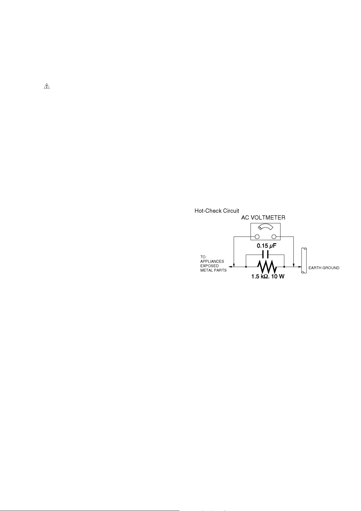
1.3. Leakage Current Hot Check
(See Figure 1.)
1. Plug the AC cord directly into the AC outlet. Do not use
an isolation transformer for this check.
2. Connect a 1.5 kΩ, 10 W resistor, in parallel with a 0.15 μF
capacitor, between each exposed metallic part on the set
and a good earth ground, as shown in Figure 1.
3. Use an AC voltmeter, with 1 kΩ/V or more sensitivity, to
measure the potential across the resistor.
4. Check each exposed metallic part, and measure the voltage at each point.
5. Reverse the AC plug in the AC outlet and repeat each of
the above measurements.
6. The potential at any point should not exceed 0.75 V RMS.
A leakage current tester (Simpson Model 229 or equivalent) may be used to make the hot checks, leakage current must not exceed 1/2 mA. In case a measurement is
outside of the limits specified, there is a possibility of a
shock hazard, and the equipment should be repaired and
rechecked before it is returned to the customer.
1.2. Leakage Current Cold Check
1. Unplug the AC cord and connect a jumper between the
two prongs on the plug.
2. Measure the resistance value, with an ohmmeter,
between the jumpered AC plug and each exposed metallic cabinet part on the equipment such as screwheads,
connectors, control shafts, etc. When the exposed metallic part has a return path to the chassis, the reading
should be between 1 MΩ and 5.2 MΩ. When the exposed
metal does not have a return path to the chassis, the
reading must be infinity.
Figure. 1
3
Page 4
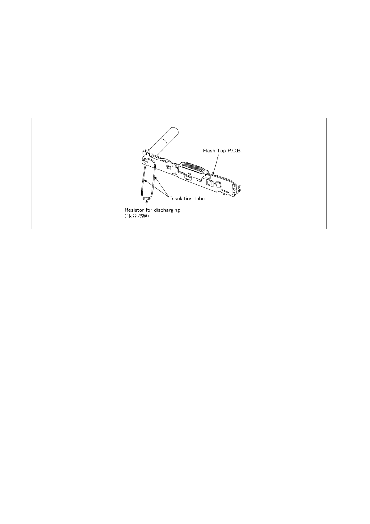
1.4. How to Discharge the Capacitor on Flash Top PCB
CAUTION:
1. Be sure to discharge the capacitor on FLASH TOP PCB.
2. Be careful of the high voltage circuit on FLASH TOP PCB when servicing.
[Discharging Procedure]
1. Refer to the disassemble procedure and Remove the necessary parts/unit.
2. Put the insulation tube onto the lead part of Resistor (ERG5SJ102:1kΩ /5W).
(an equivalent type of resistor may be used.)
3. Put the resistor between both terminals of capacitor on FLASH TOP PCB for approx. 5 seconds.
4. After discharging confirm that the capacitor voltage is lower than 10V using a voltmeter.
Fig. F1
4
Page 5
2Warning
2.1. Prevention of Electrostatic Discharge (ESD) to Electrostatically
Sensitive (ES) Devices
Some semiconductor (solid state) devices can be damaged easily by static electricity. Such components commonly are called Electrostatically Sensitive (ES) Devices.
The following techniques should be used to help reduce the incidence of compon ent damage caused by electrostatic discharge
(ESD).
1. Immediately before handling any semiconductor component or semiconductor-equipped assembly, drain off any ESD on your
body by touching a known earth ground. Alternatively, obtain and wear a commercially available discharging ESD wrist strap,
which should be removed for potential shock reasons prior to applying power to the unit under test.
2. After removing an electrical assembly equipped with ES devices, place the assembly on a condu ctive surface such as al uminum foil, to prevent electrostatic charge buildup or exposure of the assembly.
3. Use only a grounded-tip soldering iron to solder or unsolder ES devices.
4. Use only an antistatic solder removal device. Some solder removal devices not classified as "antistatic (ESD protected)" can
generate electrical charge sufficient to damage ES devices.
5. Do not use freon-propelled chemicals. These can generate electrical charges sufficient to damage ES devices.
6. Do not remove a replacement ES device from its protective package until immediately before you are ready to install it. (Most
replacement ES devices are packaged with leads electrically shorted together by conductive foam, aluminum foil or comparable conductive material).
7. Immediately before removing the protective material from the leads of a replacement ES device, touch the protective material
to the chassis or circuit assembly into which the device will be installed.
CAUTION :
Be sure no power is applied to the chassis or circuit, and observe all other safety precautions.
8. Minimize bodily motions when handling unpackaged replacement ES devices. (Otherwise harmless motion such as the
brushing together of your clothes fabric or the lifting of your foot from a carpeted floor can generate static electricity (ESD) sufficient to damage an ES device).
2.2. How to Recycle the Lithium Ion Battery (U.S. Only)
5
Page 6
2.3. Caution for AC Cord
(For EB/GC)
2.3.1. Information for Your Safety
IMPORTANT
Your attention is drawn to the fact that recording of prerecorded tapes or discs or other published or broadcast
material may infringe copyright laws.
WARNING
To reduce the risk of fire or sho ck hazard, do not expose
this equipment to rain or moisture.
CAUTION
To reduce the risk of fire or shock hazard and annoying
interference, use the recommended accessories only.
FOR YOUR SAFETY
DO NOT REMOVE THE OUTER COVER
To prevent electric shock, do not remove the cover. No user
serviceable parts inside. Refer servicing to qualified service
personnel.
2.3.2. Caution for AC Mains Lead
For your safety, please read the following text carefully.
This appliance is supplied with a moulded three-pin mains plug
for your safety and convenience.
A 5-ampere fuse is fitted in this plug.
Should the fuse need to be replaced please ensure that the
replacement fuse has a rating of 5 amperes and it is approved
by ASTA or BSI to BS1362
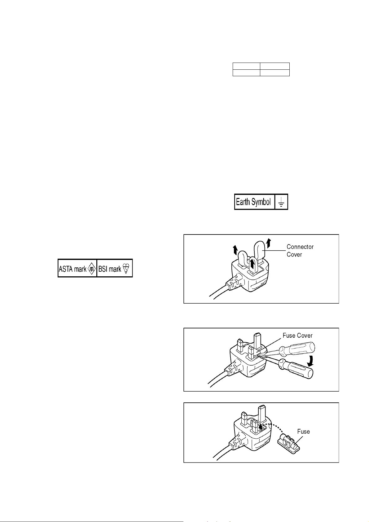
Check for the ASTA mark or the BSI mark on the body of the
fuse.
2.3.2.1. Important
The wires in this mains lead are coloured in accordance with
the following code:
Blue Neutral
Brown Live
As the colours of the wires in the mains lead of this appliance
may not correspond with the coloured markings i dentifying the
terminals in your plug, proceed as follows:
The wire which is coloured BLUE must be connected to the terminal in the plug which is marked with th e letter N or coloured
BLACK.
The wire which is coloured BROWN must be connected to the
terminal in the plug which is marked with the letter L or coloured
RED.
Under no circumstances should either of these wires be connected to the earth terminal of the three pin plug, marked with
the letter E or the Earth Symbol.
2.3.2.2. Before Use
Remove the Connector Cover as follows.
If the plug contains a removable fuse cover you must ensure
that it is refitted when the fuse is replaced.
If you lose the fuse cover, the plug must not be used until a
replacement cover is obtained.
A replacement fuse cover can be purchased from your local
Panasonic Dealer.
If the fitted moulded plug is unsuitable for the socket outlet in
your home then the fuse should be removed and the plug cut
off and disposed of safety.
There is a danger of severe electrical shock if the cut off plug is
inserted into any 13-ampere socket.
If a new plug is to be fitted please observe the wiring code as
shown below.
If in any doubt, please consult a qualified electrician.
2.3.2.3. How to Replace the Fuse
1. Remove the Fuse Cover with a screwdriver.
2. Replace the fuse and attach the Fuse cover.
6
Page 7
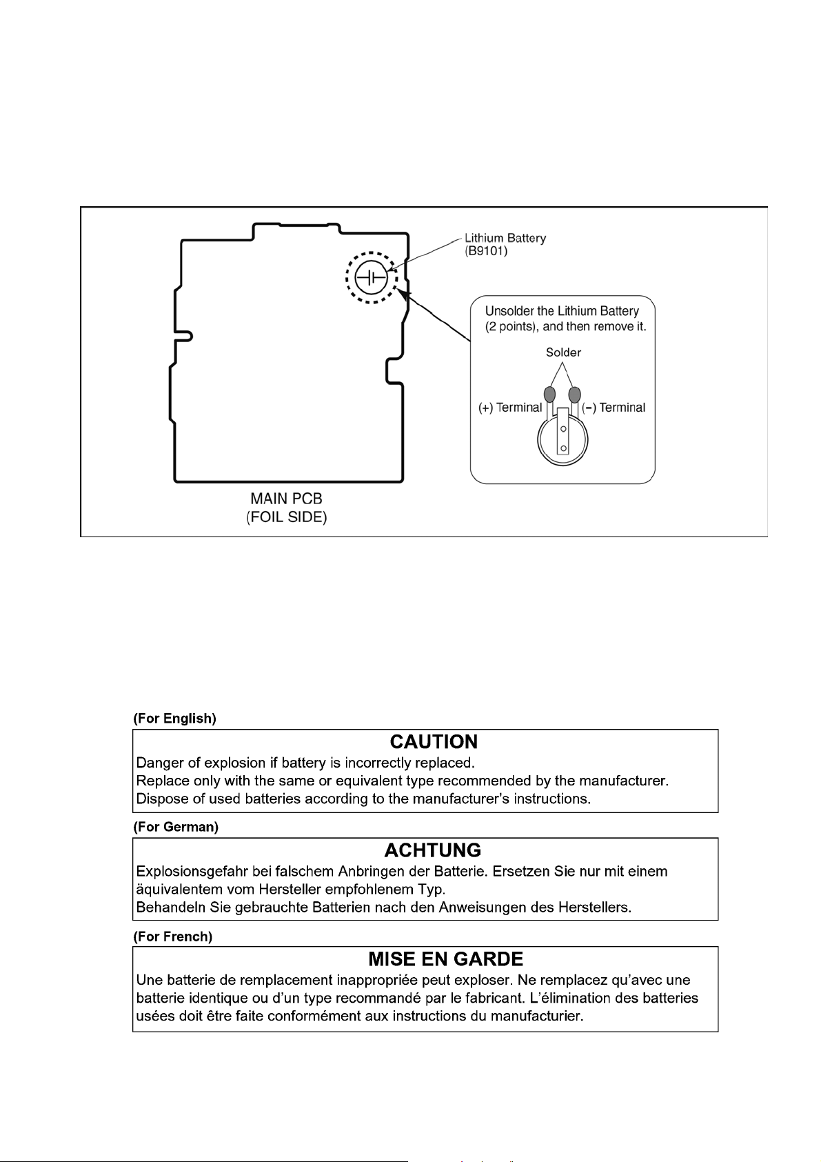
2.4. How to Replace the Lithium Battery
2.4.1. Replacement Procedure
1. Remove the MAIN PCB. (Refer to Disassembly Procedures.)
2. Unsolder the each soldering point of electric lead terminal for Lithium battery (Ref. No. “B9101” at foil side of MAIN PCB) and
remove the Lithium battery together with electric lead terminal. Then replace it into new one.
NOTE:
The Type No. ML-421S/DN includes electric lead terminals.
NOTE:
This Lithium battery is a critical component.
(Type No.: ML-421S/DN Manufactured by Ene r gy Co mpany, Panasonic Corpo r ation.)
It must never be subjected to excessive heat or discharge.
It must therefore only be fitted in requirement designed specifically for its use.
Replacement batteries must be of same type and manufacture.
They must be fitted in the same manner and location as the original battery, with the correct polarity contacts observed.
Do not attempt to re-charge the old battery or re-use it for any other purpose.
It should be disposed of in waste products destined for burial rather than incineration.
NOTE:
Above caution is applicable for a battery pack which is for DMC-FS4 series, as well.
7
Page 8
3 Service Navigation
3.1. Introduction
This service manual contains technical information, which allow service personnel’s to understand and service this model.
Please place orders using the parts list and not the drawing reference numbers.
If the circuit is changed or modified, the information will be followed by service manual to be controlled with original service manual.
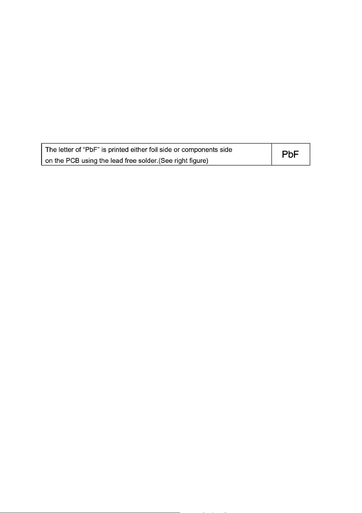
3.2. General Description About Lead Free Solder (PbF)
The lead free solder has been used in the mounting process of all electrical comp onents on the printed circuit boards us ed for this
equipment in considering the globally environmental conservation.
The normal solder is the alloy of tin (Sn) and lead (Pb). On the other hand, the lead free solder is the alloy mainly consists of tin
(Sn), silver (Ag) and Copper (Cu), and the melting point of the lead free solder is higher approx.30°C (86°F) more than that of the
normal solder.
Distinction of PCB Lead Free Solder being used
Service caution for repair work using Lead Free Solder (PbF)
• The lead free solder has to be used when repairing the equipment for which the lead free solder is used.
(Definition: The letter of “PbF” is printed on the PCB using the lead free solder.)
• To put lead free solder, it should be well molten and mixed with the original lead free solder.
• Remove the remaining lead free solder on the PCB cleanly for soldering of the new IC.
• Since the melting point of the lead free solder i s higher than that of the normal lead solder, it takes the longer time to melt the
lead free solder.
• Use the soldering iron (more than 70W) equipped with the temperature control after setting the temperature at 350±30°C
(662±86°F).
Recommended Lead Free Solder (Service Parts Route.)
• The following 3 types of lead free solder are available through the service parts route.
RFKZ03D01KS-----------(0.3mm 100g Reel)
RFKZ06D01KS-----------(0.6mm 100g Reel)
RFKZ10D01KS-----------(1.0mm 100g Reel)
Note
* Ingredient: tin (Sn) 96.5%, silver (Ag) 3.0%, Copper (Cu) 0.5%, Cobalt (Co) / Germanium (Ge) 0.1 to 0.3%
3.3. Important Notice 1:(Other than U.S.A. and Canadian Market)
1. The service manual does not contain the following information, because of the impossibility of servicing at component level
without concerned equipment/facilites.
a. Schematic diagram, Block Diagram and PCB layout of MAIN PCB.
b. Parts list for individual parts for MAIN PCB.
When a part replacement is required for repairing MAIN PCB, replace as an assembled parts. (MAIN PCB)
2. The following category is/are recycle module part. please send it/them to Central Repair Center.
• MAIN PCB (VEP56074C): Excluding replacement of Lithium Battery
8
Page 9
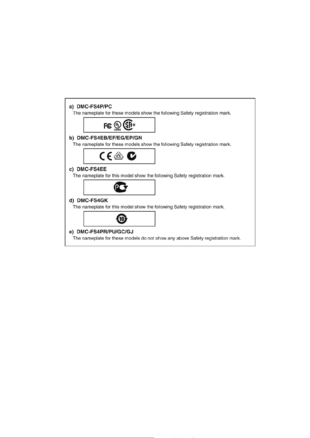
3.4. How to Define the Model Suffix (NTSC or PAL model)
There are five kinds of DMC-FS4, regardless of the colours.
• a) DMC-FS4P/PC
• b) DMC-FS4EB/EF/EG/EP/GN
• c) DMC-FS4EE
• d) DMC-FS4GK
• e) DMC-FS4PR/PU/GC/GJ
What is the difference is that the “INITIAL SETTINGS” data which is stored in Flash ROM mounted on MAIN PCB.
3.4.1. Defining methods:
To define the model suffix to be serviced, refer to the nameplate which is putte d on the bottom side of the Unit.
NOTE:
After replacing the MAIN PCB, be sure to achieve adjustment.
The adjustment instruction is available at “software download” on the “Support Information from NWBG/VDBG-A VC” web-site in
“TSN system”, together with Maintenance software.
9
Page 10
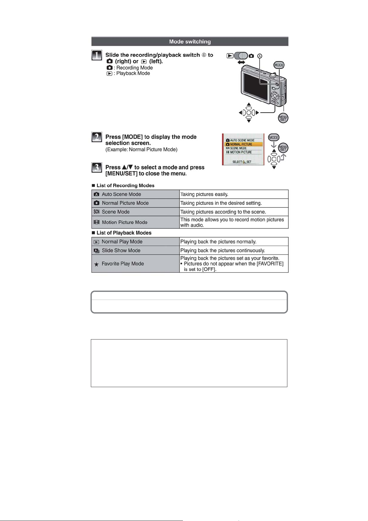
3.4.2. INITIAL SETTINGS:
After replacing the MAIN PCB, be sure to perform the initial settings after achieving the adjustment by ordering the following procedure in accordance with model suffix of the unit.
1. IMPORTANT NOTICE:
Before proceeding Initial settings, be sure to read the following CAUTIONS.
2. PROCEDURES:
• Precautions: Read the above "CAUTION 1" and "CAUTION 2", carefully.
• Preparation:
1. Attach the Battery or AC Adaptor with a DC coupler to the unit.
2. Set the recording mode to the [NORMAL PICTURE] mode.
(Press the [MODE] button and select the [NORMAL PICTURE] by pressing the “[ UP ] and [DOW N] of Cursor buttons”,
then press the [MENU/SET] button.)
NOTE:
If the unit is other than [NORMAL PICTURE] mode, it does not display the initial settings menu.
• Step 1. The temporary cancellation of “INITIAL SETTINGS”:
Set the [REC]/[PLAYBACK] selector switch to “[ REC ] (Camera mark)”.
While keep pressing “[ UP ] of Cursor button” and [ DISPLAY ] button simultaneously, turn the Power on.
• Step 2. The cancellation of “INITIAL SETTINGS”:
Set the [REC]/[PLAYBACK] selector switch to “[ PLAYBACK ]”.
Press “[ UP ] of Cursor button” and [ DISPLAY ] button simultaneously, then turn the Power off.
• Step 3. Turn the Power on:
Set the [REC]/[PLAYBACK] selector switch to “[ REC ] (Camera mark)”, and then turn the Power on.
• Step 4. Display the INITIAL SETTING:
NOTE:
If the unit is other than [NORMAL PICTURE] mode, it does not display the initial settings menu.
While keep pressing [ MENU/SET ] and “[ RIGHT ] of Cursor buttons” simultaneously, turn the Power off.
The "INITIAL SETTINGS" menu is displayed.
There are two kinds of “INITIAL SETTINGS” menu form as follows:
10
Page 11
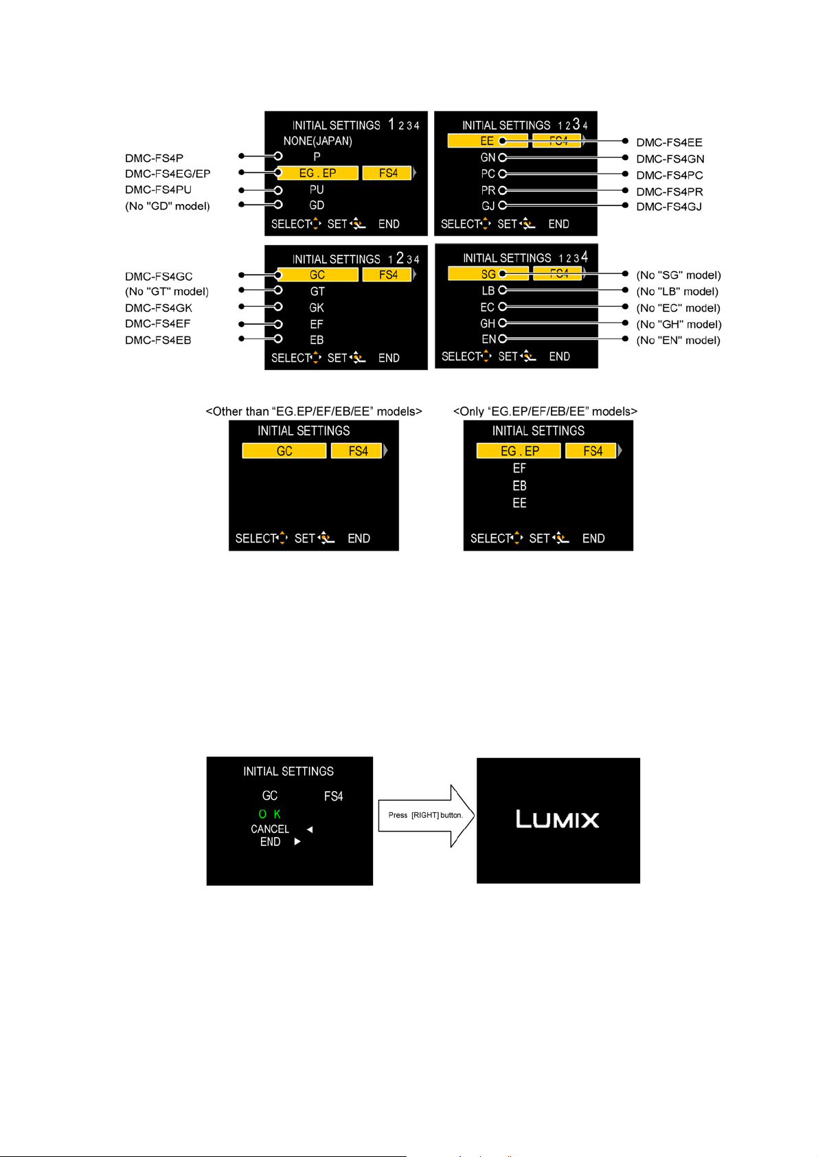
[CASE 1. After replacing MAIN P.C.B.]
When MAIN P.C.B. has just been replaced, all of the model suffix is displayed as follows. (Four pages in total)
[CASE 2. Other than “After replacing MAIN P.C.B.”]
• Step 5. Choose the model suffix in “INITIAL SETTINGS”: (Refer to “CAUTION 1”)
[Caution: After replacing MAIN P.C.B.]
The model suffix can been chosen, JUST ONE TIME.
Once one of the model suffix have been chosen, the model suffix lists will not be displayed, thus, it can be changed.
Therefore, select the area carefully.
Select the area with pressing “[ UP ] / [ DOWN ] of Cursor buttons”.
• Step 6. Set the model suffix in “INITIAL SETTINGS”:
Press the “[ RIGHT ] of Cursor buttons”.
The only set area is displayed, and then press the “[ RIGHT ] of Cursor buttons” after confirmation.
(The unit is powered off automatically.)
11
Page 12

• Step 7. CONFIRMATION:
Confirm the display of “PLEASE SET THE CLOCK” in concernd language when the unit is turned on again.
When the unit is connected to PC with USB cable, it is detected as removable media.
1) As for your reference, major default setting condition is as shown in the following table.
• Default setting (After “INITIAL SETTINGS”)
MODEL VIDEO OUTPUT LANGUAGE DATE REMARKS
a) DMC-FS4P NTSC English Month/Date/Year
b) DMC-FS4EG PAL English Date/Month/Year
c) DMC-FS4EP PAL English Date/Month/Year
d) DMC-FS4PU NTSC English Month/Date/Year
e) DMC-FS4GC PAL English Date/Month/Year
f) DMC-FS4GK PAL Chinese (simplified) Year/Month/Date
g) DMC-FS4EF PAL French Date/Month/Year
h) DMC-FS4EB PAL English Date/Month/Year
i) DMC-FS4EE PAL Russian Date/Month/Year
j) DMC-FS4GN PAL English Date/Month/Year
k) DMC-FS4PC NTSC English Month/Date/Year
l) DMC-FS4PR PAL English Date/Month/Year
m) DMC-FS4GJ PAL Thai Date/Month/Year
12
Page 13
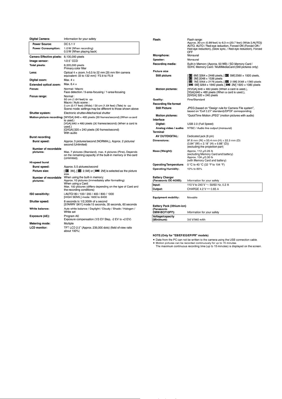
4 Specifications
13
Page 14
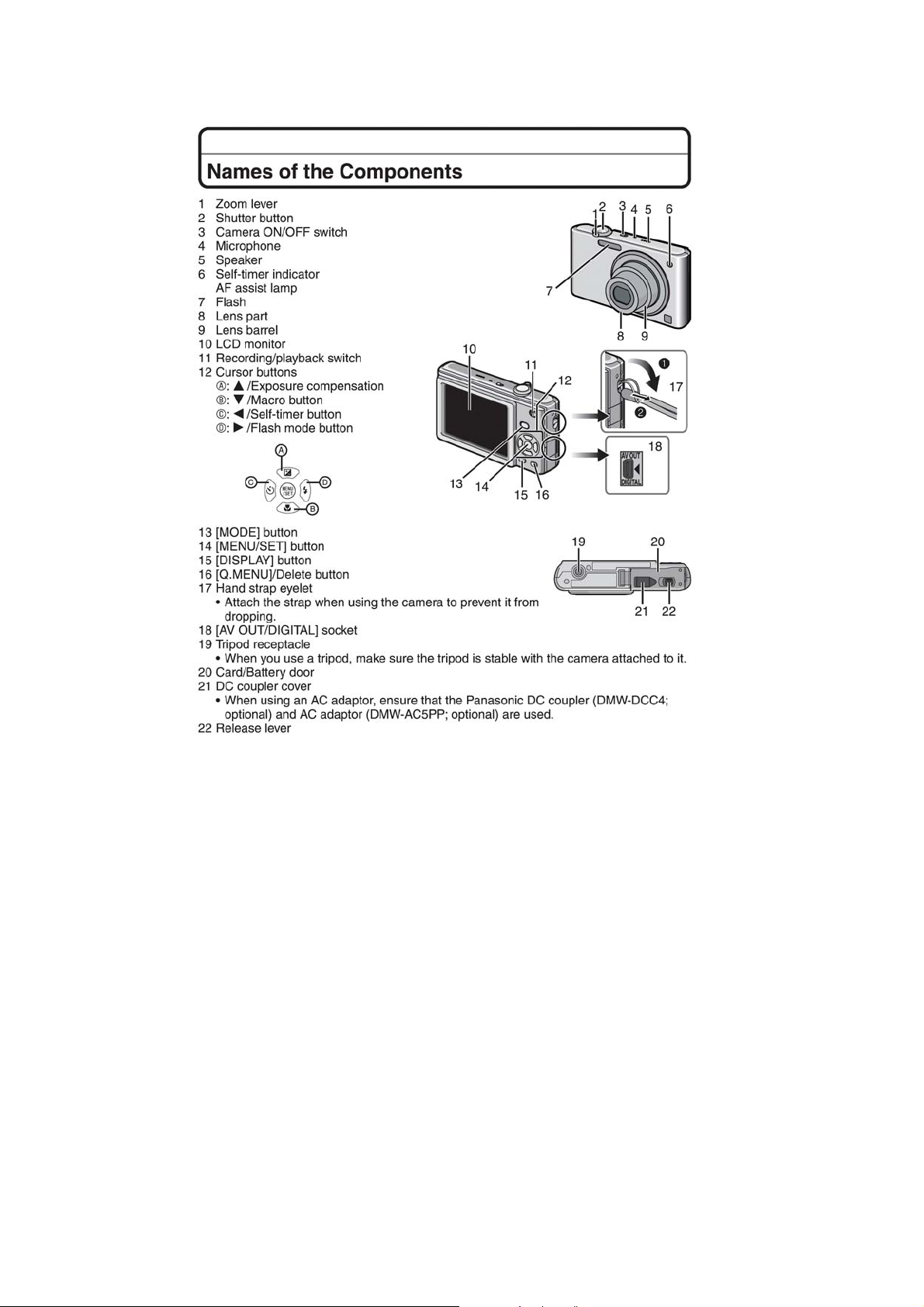
5 Location of Controls and Components
14
Page 15
Preparation
About the Battery
This unit has a function that can distinguish useable batteries. Exclusive batteries
are supported by this function. (Conventional batteries not supported by this function
cannot be used.)
It has been found that counterfeit battery packs which look very similar to the
genuine product are made available to purchase in some markets. Some of these
battery packs are not adequately protected with internal protection to meet the
requirements of appropriate safety standards. T
battery packs may lead to fire or explosion. Please be advised that we are not
liable for any accident or failure occurring as a result of use of a counterfeit
battery pack. To ensure that safe products are used we would recommend that a
genuine Panasonic battery pack is used.
here is a possibility that these
15
Page 16
6 Service Mode
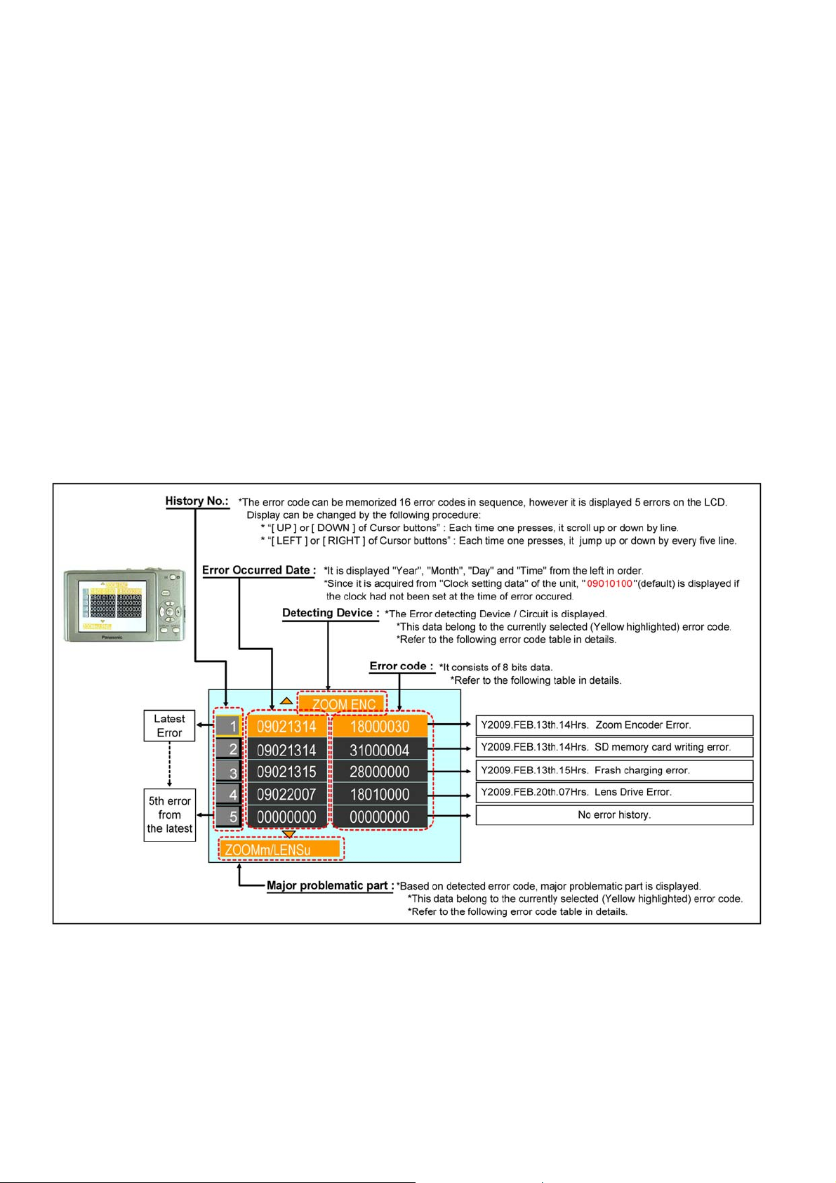
6.1. Error Code Memory Function
1. General description
This unit is equipped with history of error code memory function, and can be memorized 16 error codes in sequence from the
latest. When the error is occurred more than 16, the oldest error is overwritten in sequence.
The error code is not memorized when the power supply is shut down forcibly (i.e.,when the unit is powered on by the battery,
the battery is pulled out) The error code is memorized to FLASH ROM when the unit has just before powered off.
2. How to display
The error code can be displayed by ordering the following procedure:
• Preparation:
1. Attach the Battery or AC Adaptor with a DC coupler to the unit.
NOTE:
*Since this unit has built-in memory, it can be performed without inserting SD memory card.
*It is not a matter of the setting condition of Recording mode (such as "normal picture/ Auto Scene / scene mode) to display
the error code.
• Step 1. The temporary cancellation of “INITIAL SETTINGS”:
Set the [REC]/[PLAYBACK] selector switch to “[ REC ] (Camera mark)”.
While keep pressing “[ UP ] of Cursor button” and [ DISPLAY ] button simultaneously, turn the Power on.
• Step 2. Execute the error code display mode:
Press the “[ LEFT ] of Cursor button”, [ MENU/SET ] button and [ DISPLAY ] button simultaneously.
The display is changed as shown below when the above buttons are pressed simultaneously.
Normal display → Error code display → Operation history display → Normal display → .....
Example of Error Code Display
16
Page 17

• 3. Error Code List
The error code consists of 8 bits data and it shows the following information.
Important notice about "Error Code List"
1) About "*" indication:
The third digit from the left is different as follows.
- In case of 0 (example: 180
When the third digit from the left shows "0", this error occurred under the condition of INITIAL SETTINGS has been
completed.
It means that this error is occurred basically at user side.
- In case of 8 (example: 188
When the third digit from the left shows "8", this error occurred under the condition of INITIAL SETTINGS h as been
released.
(Example; Factory assembling-line before unit shipment, Service mode etc.)
It means that this error is occurred at service side.
2) About "?" indication: ("18*0 0?01" to "18*0 0?50"):
The third digit from the right shows one of the hexadecimal ("0" to "F") character.
01000)
01000)
17
Page 18

• 4. How to exit from Error Code display mode:
Simply, turn the power off. (Since Error code display mode is executed under the condition of temporary cancellation of "INITIAL SETTINGS", it wake up with normal condition when turn off the power.)
NOTE:
The error code can not be initialized.
18
Page 19

7 Service Fixture & Tools
7.1. Service Fixture and Tools
The following Service Fixture and tools are used for checking and servicing this unit.
19
Page 20

7.2. When Replacing the Main PCB
After replacing the MAIN PCB, be sure to achieve adjustment.
The adjustment instruction is available at “software download” on th e “Support Information from NWBG/VDBG-AVC” web-site in
“TSN system”, together with Maintenance software.
7.3. Service Position
This Service Position is used for checking and replacing parts. Use the following Extension cables for servicing.
Table S1 Extension Cable List
No. Parts No. Connection Form
1 RFKZ0416 FP9001 (MAIN) - CCD UNIT 41PIN 0.3 FFC
2 RFKZ0477 FP9002 (MAIN) - LENS UNIT 45PIN 0.3 FFC
3 RFKZ0418 PP9001 (MAIN) - PS8001 (FLASH TOP) 30PIN B to B
CAUTION-1. (When servicing FLASH TOP PCB)
1. Be sure to discharge the capacitor on FLASH TOP PCB.
Refer to “HOW TO DISCHARGE THE CAPACITOR ON FLASH TOP PCB”.
The capacitor voltage is not lowered soon even if the AC Cord is unplugged or the battery is removed.
2. Be careful of the high voltage circuit on FLASH TOP PCB.
3. DO NOT allow other parts to touch th e hi g h vol tage circuit on FLASH TOP PCB.
20
Page 21

8 Disassembly and Assembly Instructions
8.1. Disassembly Flow Chart
8.2. PCB Location
21
Page 22

8.3. Disassembly Procedure
No. Item Fig Removal
1 Rear Case Unit
Front Case Unit
2 LCD Unit (Fig.D3) 1 Locking tab (A)
3 Top Operation Unit (Fig.D5) PS8001(Connector)
4 Flash Top P.C.B. (Fig.D6) AF Panel Light
5 Lens Unit (Fig.D9) FP9001(Flex)
6 Main P.C.B. (Fig.D10) 1 Screw (F)
7 SD FPC Unit (Fig.D11) 1 Screw (G)
8 Battery Case Unit (Fig.D12) Earth Plate
9 Battery Door Unit (Fig.D14) Battery Door Shaft
(Fig.D1) Card
Battery
1 Screw (A)
5 Screws (B)
3 Locking tabs
Rear Case Unit
(Fig.D2) 4 Locking tabs
Jack Door
Tripod Fixing Plate
Front Case Unit
2 Locking tabs (B)
(Fig.D4) 3 Screws (C)
1 Screw (D)
3 Ribs
Frame Plate
FP9103(Flex)
LCD Unit
Top Operation Unit
2 Screws (E)
5 Locking tabs
(Fig.D7) Top Ornament Unit
Speaker Unit
Mic Damper
Power Knob Base
Power Knob
Flash Top P.C.B.
(Fig.D8) NOTE: (When installing)
FP9002(Flex)
Lens Unit
FP9005(Flex)
1 Locking tab
Main P.C.B.
SD FPC Unit
2 Locking tabs
1 Rib
(Fig.D13) Battery Out Spring
Battery Case Unit
Battery Door Spring
Battery Door Unit
8.3.1. Removal of the Rear Case Unit and
Front Case Unit
22
(Fig.D1)
Page 23

(Fig.D2)
8.3.2. Removal of the LCD Unit
(Fig.D3)
(Fig.D4)
23
Page 24

8.3.3. Removal of the Top Operation Unit
(Fig.D5)
8.3.4. Removal of the Flash Top P.C.B.
(Fig.D6)
(Fig.D7)
24
Page 25

(Fig.D8)
8.3.6. Removal of the Main P.C.B.
8.3.5. Removal of the Lens Unit
(Fig.D10)
8.3.7. Removal of the SD FPC Unit
(Fig.D9)
(Fig.D11)
25
Page 26

8.3.8. Removal of the Battery Case Unit
8.3.9. Removal of the Battery Door Unit
(Fig.D14)
NOTE: (When Assembling)
Be sure to confirm the following points when assembling.
• The Screw is tightened enough.
• Assembling conditions are fine. (No distortion, no illegalspace.)
• No dust and/or dirt on every Lens surfaces.
• LCD image is fine. (No dust and dirt on it, and no gradient
images.)
(Fig.D12)
(Fig.D13)
26
Page 27

8.4. Disassembly Procedure for the
Lens
NOTE: When Disassembling and Assembling for the Lens
1. To minimize the possibility of the CCD bein g dirt, perform
disassemble and/or assemble under the condition of the
CCD is being mounted.
Disassembling procedures for the CCD unit, refer to item
8.6.
2. Take care that the dust and dirt are not entered into the
lens.
In case of the dust is putted on the lens, blow off them by
airbrush.
3. Do not touch the surface of lens.
4. Use lens cleaning KIT (BK)(VFK1900BK).
5. Apply the grease (RFKZ0472) to the point where is
shown to “Grease apply“ in the figure.
When the grease is applied, use a toothpick and apply
thinly.
6. When repair the drive frame, drive frame and direct
frame, must be unit exchange.
8.4.1. Removal of the Zoom Motor Unit
and Lens FPC P.C.B. Unit
1. Peal the 3 barrier sheets.
2. Remove the 1 solder (A).
3. Remove the 3 locks.
4. Unscrew the 2 screws (A).
5. Remove the zoom motor unit to the indicated by arrow.
6. Remove the 1 solder (B).
7. Unscrew the 1 screw (B).
8. Remove the lens flex to the indicated by arrow.
27
Page 28

8.4.2. Removal of the Master Flange Unit 8.4.3. Removal of the 1st Lens Frame/2nd
Lens Frame Move Unit
8.4.4. Removal of the 2nd Lens Frame
Move Unit
28
Page 29

8.4.5. Removal of the Drive/Direct Frame
Unit
8.5. Assembly Procedure for the
Lens
8.5.1. Phase alignment of the Direct
Frame and Drive Frame Unit
8.5.2. Phase alignment of the Drive/Direct
Frame Unit and Fixed Frame Unit
29
Page 30

8.5.3. Assembly for the 1st Lens Frame
Unit and Fixed/Drive/Direct Frame
Unit
8.5.4. Assembly for the 2nd Lens Frame
Move Unit and Fixed/Drive/Direct
Frame/1st Lens Frame Unit
30
Page 31

8.5.5. Assembly for the Master Flange
Unit and Fixed/Drive/Direct Frame/
1st Lens Frame/2nd Lens Frame
Move Unit
8.6. Removal of the CCD Unit
To prevent the CCD unit from catching the dust and dirt, do not
remove the CCD unit except for replacing.
31
Page 32

8.7. Removal of the Focus Motor
8.8. The Applyment of Grease
Unit
Method
The grease apply point of lens unit are as follows.
Apply grease additionally in the specified position if necessary.
When the grease is applied, use a toothpick and apply thinly.
• Guide pole/Fasten groove of nut/Focus motor unit (Lead
screw)
- Grease: RFKZ0472
- Amount of apply: 2 - 4 mg
32
Page 33

9 Measurements and Adjustments
9.1. Matrix Chart for Replaced Part and Necessary Adjustment
The relation between Replaced part and Necessary Adjustment is shown in the following table.
When concerned part is replaced, be sure to achieve the necessary adjustment(s).
As for Adjustment condition/procedure, consult the “Adjustment Manual” which is available in Adjustment software.
The Adjustment software is available at “TSN Website”, therefore, access to “TSN Website” at “Support Information from NWBG/
VDBG-AVC”.
NOTE:
After adjustments have been terminated, make sure to achieve “INITIAL SETTINGS”.
Replaced Part
CCD Unit
-
*1
O
*1
O
*1
O
Camera
Section
Adjustment Item
OIS hall element adjustment
(OIS)
Back focus adjustment
(BF)
Shutter adjustment
(SHT)
ISO sensitivity adjustment
(ISO)
AWB adjustment
High brightness coloration inspection
(WBL)
CCD white scratch compensation
(WKI)
CCD black scratch compensation
(BKI)
Venus zoom inspection
(PZM)
Monitor linearity inspection
(MLN)
Colour reproduction inspection
MIC inspection
(COL)
Main P.C.B. VENUS
(IC6001)
OOOO
OOOO
OOOOO
OOOOO
OOOOO
OOO
OOO
OOO
OOOOO
OOOOO
Flash-ROM
(IC6002)
*1: This adjustment is necessary, not only replacing CCD unit but also removing it from the lens unit.
NOTE:
*There is no LCD adjustment in this model.
Lens Part
(Excluding
CCD)
-
-
--
33
Page 34

10 Maintenace
10.1. Cleaning Lens and LCD Panel
Do not touch the surface of lens and LCD Panel with your hand.
When cleaning the lens, use air-Blower to blow off the dust.
When cleaning the LCD Panel, dampen the lens cleaning paper with lens cleaner, and the gently wipe the their surface.
Note:
The Lens Cleaning KIT ; VFK1900BK (Only supplied as 10 set/Box) is available as Service Aid.
34
Page 35

Table of contents
Service Manual
DSC0903022CE
Diagrams and Replacement
Parts List
Vol. 1
(S)...........Silver Type (except PC/EF/GJ)
Colour
(K)...........Black Type
Model No.
DMC-FS4P
DMC-FS4PC
DMC-FS4PR
DMC-FS4PU
DMC-FS4EB
DMC-FS4EE
DMC-FS4EF
DMC-FS4EG
DMC-FS4EP
DMC-FS4GC
DMC-FS4GJ
DMC-FS4GK
DMC-FS4GN
Digital Camera
Name of Signal
OFTR
FEP
This signal is connected
to the FEP schematic diagram.
Circuit name being connected.
6.Use the parts number indicated on the Replacement Parts List .
7.Indication on Schematic diagrams:
5.The voltage being indicated here may be include observational-error (deviation) due to
internal-resistance and/or reactance of equipment. Therefore, handle the value
indicated on here as reference.
4.Although the voltage and waveform available on here is measured with standard frame,
it may be differ from actual measurement due to modification of circuit and so on.
3.The voltage being indicated on the schematic diagram is measured in
"Standard-Playback" mode when there is no specify mode is mentioned.
2.It is only the "Test Round" and no terminal (Pin) is available on the P.C.B.
when the TP (Test Point) indicated as " " mark.
1.Although reference number of the parts is indicated on the P.C.B. drawing and/or
schematic diagrams, it is NOT mounted on the P.C.B. when it is displayed with "$" mark.
FOR SAFETY. WHEN REPLACING ANY OF THESE COMPONENTS USE ONLY THE SAME TYPE.
COMPONENTS IDENTIFIED WITH THE MARK HAVE THE SPECIAL CHARACTERISTICS
S1. About Indication of The Schematic Diagram
S1.1. Important Safety Notice
S1. About Indication of The Schematic Diagram ............................ S-1
S1.1. Important Safety Notice......................................................... S-1
S2. Voltage Chart ........................................................................... S-2
S2.1. Flash Top P.C.B. ....................................................................S-2
S3. Block Diagram .......................................................................... S-3
S3.1. Overall Block Diagram ..........................................................S-3
S4. Schematic Diagram .................................................................. S-4
S4.1. Interconnection Diagram ....................................................... S-4
S4.2. Flash Top Schematic Diagram .............................................. S-5
S4.3. CCD Flex Schematic Diagram .............................................. S-6
S4.4. Lens Flex Schematic Diagram .............................................. S-7
S5. Print Circuit Board .................................................................... S-8
S5.1. Flash Top P.C.B. ....................................................................S-8
S5.2. CCD Flex P.C.B. .................................................................... S-9
S5.3. Lens Flex P.C.B. .................................................................. S-10
S6. Replacement Parts List .......................................................... S-11
S7. Exploded View .......................................................................S-15
S7.1. Frame and Casing Section.................................................. S-15
S7.2. Packing Parts and Accessories Section (1) ........................ S-16
S7.3. Packing Parts and Accessories Section (2) ........................ S-17
S-1
Page 36

S2. Voltage Chart
Note) Indicated voltage values are the standard values for the unit measured by the DC electronic circuit tester (high-impedance) with the chassis taken as standard.
Therefore, there may exist some errors in the voltage values, depending on the internal impedance of the DC circuit tester.
S2.1. Flash Top P.C.B.
REF No.
IC8001 1 5.8
IC8001 2 0
IC8001 3 0
IC8001 4 0
IC8001 5 5.8
Q8009 1 6.9
Q8009 2 6.9
Q8009 3 0
Q8009 4 0
Q8009 5 6.9
Q8009 6 6.9
PIN No. POWER ON
S-2
Page 37

S3. Block Diagram
CCD
IC3001
CCD SIGNAL
PROCESSOR
FOCUSIRIS
SDRAM/256Mbit
NAND FLASH ROM/512Mbit
SD
CARD
(POWER SUPPLY)
BATTERY
REAR OPERATION UNIT
DMC-FS4 OVERALL BLOCK DIAGRAM
IC9101
SYSTEM IC
MOTOR DRIVE,
OIS DRIVE&
PRE PROCESS
IC6001
VENUS4
CAMERA PROCESS
J-PEG COMP/EX PANDS
MEDIA I/F
USB I/F
MAIN MICROPROCESSOR
FLASH
TOP OPERATION UNIT
IC1001
POWER
SHUTTER
IC9101
SYSTEM IC
IC6002
ZOOM
OIS CONTROL
LENS DRIVE
LCD DRIVE
AV OUT / DIGITAL
TERMINAL
COLOR LCD
PANEL
(33mm ~ 132mm)
IC9101
SYSTEM IC
MICROPHONE
MICROPHONE AMP
SPEAKER CONTROL
SPEAKER
1/2.5" 8 MEGA PIX
CDS, AGC,
A/D, TG,
CCD DRIVER
2.5" PANEL
230k dots
X6001
(24MHz)
X9101
(32.768kHz)
VIDEO OUT
IC8001
IGBT DRIVER
IC6004
FeRAM
IC3002
REGLATOR
IC1210
REGLATOR
S3.1. Overall Block Diagram
S-3
Page 38

S4. Schematic Diagram
DMC-FS4 INTERCONNECTION DIAGRAM
FP9001
FP9002
1
2
3
5
6
7
8
4
9
11
10
13
14
12
15
16
17
18
19
20
21
22
23
24
25
26
27
28
29
30
31
32
33
34
35
36
37
38
39
LCD UNIT
MAIN P.C.B.
(COMPONENT SIDE)
: (FOIL SIDE)
PS8001
123
4
5
6
7
8
9
10
11
121314
15 16
171819
2021222324
2526272829
30
P8002
3
2
1
PP9001
BATTERY
FLASH TOP P.C.B.
(COMPONENT SIDE)
STB CHG LV
MIC GND
MIC IN
A GND
MIC REG
SHUTTER 1
SHUTTER 0
ID BAT DQ
UNREG GND
PO
WER ON L
AI SW
UNREG
UNREG
UNREG
UNREG
SPEAKER
ET8002
ET8001
M8001
MICROPHONE
STB PWM OUT
FLASH
TRG
CA
THODE
ANODE
SP NEG
SP POS
BA
TT THERMO
TELE
WIDE
IGBT VCC
UNREG GND
UNREG GND
UNREG GND
UNREG GND
REC PB MODE
FRAME GND
STB CHG LV
MIC GND
MIC IN
A GND
MIC REG
SHUTTER 1
SHUTTER 0
ID BAT DQ
UNREG GND
POWER ON L
IA SW
UNREG
UNREG
UNREG
UNREG
1
2
345
6
7
8
9
10
111213
14
15
30
292827
26
25
242322
21
201918
17
16
41
40
CCD
UNIT
LENS
UNIT
1
2
3
5
6
7
8
4
9
11
10
13
14
12
15
16
17
18
19
20
21
22
23
24
25
26
27
28
29
30
31
32
33
34
35
36
37
38
39
41
40
CON CHK
SUBSW2
V9R
V11R
V12
V11B
V9
V7
V6
V5B
NC
V4
V2
CCD GND
CCD OUT
CCD GND
SUB SW1
CCD GND
HL
H2
CON CHK
CCD THERMO
MSUBSW
V9L
V11L
V11A
V10
V8
V7S
V5A
VL
VH
V1
V3
CCD GND
CCD GND
MSUB
SUB
R
H1
CCD GND
FP9103
43
45
42
44
FP9005
SDDAT2
SDCMD
SDDAT1
D GND
D GND
D3V
FRAME GND
SDCD
SDDAT3
SDDAT0
SDWP
D GND
SDCLK
FRAME GND
FRAME GND
14
12
10
8
6
4
2
15
13
11
9
7
5
3
1
: (FOIL SIDE)
SD FPC UNIT
ENC VCC
ABS
NC
STAP
STAN
SH+
SH
-
ZM2
ZM1
NC
1-ABS
2-LED CONT
NC
FBN
FAP
FAN
LED CONT
STAP
STAN
SH+
SH
-
NC
ZM2
ZM1
1-LED CONT
ENC VCC
2-ABS
FBN
FAP
FBP
1
2
3
5
6
7
8
4
9
11
10
13
14
12
15
16
17
18
19
20
21
22
23
24
25
26
27
28
29
30
31
32
33
34
35
36
37
38
39
41
40
CP3
CP5
CP7
NC
PCD
VCOMH
NC
CP1
NC
LED
LED
VCC
LCDHD
LCDOUT0
LCDOUT2
LCDOUT4
LCDOUT6
S SYSCON SO
LCD CS
LCD RESET
BLMINUS
CP4
CP6
CP8
VCC 1.8
VCOML
AGND
AVDD
CP2
FB
NC
GND
LCD VD
CLK18 LCD
LCDOUT1
LCDOUT3
LCDOUT5
LCDOUT7
S SYSCON SCK
SHDB
BL PLUS
STB PWM OUT
FLASH TRG
CATHODE
ANODE
SP NEG
SP POS
BATT THERMO
TELE WIDE
IGBT VCC
UNREG GND
UNREG GND
UNREG GND
UNREG GND
REC PB MODE
FRAME GND
4
UNREG
BAT THERMO
ID BAT DQ
UNREG GND
NC
NC
NC
NC
NC
NC
NC
NC
NC
NC
NC
NC
NC
NC
NC
S4.1. Interconnection Diagram
S-4
Page 39

S4.2. Flash Top Schematic Diagram
CL8003
CL8011
CL8008
CL8005
CL8026
CL8004
CL8010
TL8003
TL8001
TL8002
TL8007
TL8004
ET8003
VMB4149
3 2 1
4 5 6
Q8009
B1DFCG000020
R8002
100K[18]
1M[36]
R8006
R8021
15K
R8032
1M[D]
[22]
R8033
1M[D]
[22]
R8013
15K[D]
R8003
56[18]
R8036
10k
R8004
$(0)
R8038
22
R8037
22
1 2
3 4
5
6
K0F212A00003
S8001
57
41236
S8002
K0D112B00145
5 7
4 1 2 3 6
S8005
K0D112B00145
2 3
1 4
S8003
K0L1CB000003
2 1
3
G5F1A0000026
L8001
J0JCC0000415
LB8001
L0CBAA000012
M8001
C8009
F1J0J106A020
6.3V
0.1
C8001
10V
C8006
F1K2E4730005
[36]
250V
C8007
$
[36]
F1K2J102A028
C8004
630V
C8014
F1G1A1040006
10V
C8017
$[F1G0J1050007]
C8015
D4ED18R00008
D4ED18R00008
C8016
1 2
34
T8001
G5D1A0000066
Confidential
Until
ET8001
K4AC01D00001
K4AC01D00001
ET8002
N9ZZ00000333
ET8004
6
7
5
9
13
10
12
11
14
15
8
1
3
4
2
25
28
30
29
26
27
21
22
18
16
17
20
19
24
23
K1KB30AA0123
PS8001
C8003
F2A2F9500002
300V95uF
315V
5
43
2
1
C0ZBZ0001636
IC8001
1
2
3
B0EDAT000002
D8002
1
243
5
6
7
8
B1JBLP000023
Q8001
F8021
K5H152200006
ERBSE1R25U
F8001
1
3
4
2
K4ZZ04000051
P8002
$[D4ED18R00008]
VA8001
D8001
B3ADA0000229
LAMP[+]LAMP[-]
#S
#S
TRG_G TRG FIRST
S
S
S
D
G
TRG SECOND
SLEEVE_GND
OFFON
BAT_THERMO
BAT_THERMO
F
F
STB_CHG_LV
MIC_GND
A_GND
MIC_IN
MIC_REG
SHUTTER_1
SHUTTER_0
UNREG_GND
UNREG_GND
UNREG_GND
UNREG_GND
UNREG_GND
UNREG_GND
SP_NEG
SP_POS
TELE_WIDE
FRAME_GND
STB_PWM_OUT
STROBE_TRG
SAFETY_GND
POWER_ON_L
IGBT_VCC
ANODE
CATHODE
REC_PB_MODE
GND
INA
INB
OUT
VCC
T/W_SW
SHUTTER_SW
REC/PB_SW
REC
PB
UNREG
UNREG
UNREG
UNREG
UNREG
ID_BAT_DQ
ID_BUT_DQ
(3.4V)
or
DELETED
B3ADA0000215(LS85)の時
22ohm X 2
NC(IASW)
IA_SW
HFO803165CP(D6)(R)-S2
CAUTION: FOR CONTINUED PROTECTION AGAINST FIRE HAZARD,
REPLACE ONLY WITH THE SAME TYPE 1.5A 32V FUSE.
ATTENTION: POUR UNE PROTECTION CONTINUE LES RISQUES
D' INCENDIE N' UTILISERQUE DES FUSIBLE DE MÉME TYPE 1.5A 32V.
1.5A 32V
1.5A 32V
CAUTION: FOR CONTINUED PROTECTION AGAINST FIRE HAZARD,
REPLACE ONLY WITH THE SAME TYPE 1.25A 32V FUSE.
ATTENTION: POUR UNE PROTECTION CONTINUE LES RISQUES
D' INCENDIE N' UTILISERQUE DES FUSIBLE DE MÉME TYPE 1.25A 32V.
1.25A 32V
1.25A 32V
DMC-FS4
Flash Top
Schematic Diagram
10987654321
G
F
E
D
C
B
A
S-5
Page 40

S4.3. CCD Flex Schematic Diagram
231
546
UP05C8B00L
Q3101
R3107
1300
R3108
22
R3102
1800
R3101
47
ECJ1VB1C105K
C3101
F1H1A225A051
C3103
[18]
1
9
7
5
3
2
4
6
8
41
37
38
36
40
39
33
34
29
30
25
26
21
22
17
18
13
14
11
10
12
16
15
20
19
24
23
28
27
32
31
35
FT3101
TH3101
D4CC11030026
43 521 9 76 8 10
313340 38 36 34353739 32
2015 17 18161311 12 14 19
2224262830 29 27 25 23 21
MN34500PLH-V
IC3101
V6
V6
V2
V2
V4V4V5B
V5B
V7S
V7S
V7V7V8V8V9
V9
V5A
V5A
V3
V3
V1
V1
V11B
V11B
V10
V10
V11A
V11A
V12
V12
SUB
SUB
V11R
V11R
R
R
HL
HL
H1
H1
H2
H2
V9L
V9L
SUBSW
SUBSW
MSUB
MSUB
V9R
V9R
V11LV11L
V11L
C
R
BGE
D
S
CCD_GND
CCD_GND
CCD_GND
CCD_GND
CCD_GND
CCD_GND
CON_CHK
CON_CHK
H1
HL
HL
H2
V2
V2
PT
V8
V8
V10
V10
V9
V9
CCD_THERMO
SUB
SUB
MSUB
MSUB
SUBSW1
CCD_OUT
SUBSW2
MSUBSW
<Vdr NET Name Rule>
[CCD_10M]_[CCD_8M]
V4
V4
VH
NC
NC
NC
NC
NC
NC
NC
NC
NC
VL
V7S
V7S
V12
V12
V11L
V11L
V11R
V11R
V9L
V9L
V9R
V9R
V1B_V5B
V1A_V5A
V6
V6
V7B_V11B
V7A_V11A
V7
V5A
V5B
V3
V1
VO
VDD
RG
H1A
H2A
SUBSW
GND
H1B
H2B
V11A
V11B
V3AV3B_V3
V5AV5B_V1
V11_V7
DMC-FS4
CCD Flex
Schematic Diagram
10987654321
G
F
E
D
C
B
A
S-6
Page 41

S4.4. Lens Flex Schematic Diagram
A
B
C
D
E
F
G
654321
5
6
7
8
13
14
15
24
25
28
29
26
27
21
22
36
37
38
39
4
3
2
1
PHOTO
SENSOR
ZOOM ENCODER 1
CO. BARREL ENCODER
(FULL RETRACT)
DC SOLENOID
(IRIS)
D
A
10
11
9
12
16
17
18
19
20
23
30
31
32
33
34
35
DC SOLENOID
(SHUTTER)
SHUTTER UNITB
POSITIVE VOLTAGE LINE
DMC-FS4 LENS FLEX SCHEMATIC DIAGRAM
TO MAIN
(MAIN CN) CIRCUIT
(FP9002)
A2
A1
B2
B1
B4
B3
STEPPING
MOTOR
FOCUS MOTOR UNIT
F
40
41
A3
F1
F2
F3
F4
COIL
COIL
DC MOTOR
ZOOM MOTOR UNIT
C
PHOTO
SENSOR
ZOOM ENCODER 2
E
PHOTO
SENSOR
42
43
44
45
ENC VCC
LED CONT
ABS
NC
NC
NC
NC
NC
NC
STAP
STAP
SH+
SH+
SH
-
SH
-
NC
ZM2
ZM2
ZM1
ZM1
NC
1-LED CONT
1-ABS
ENC VCC
2-LED CONT
2-ABS
NC
FBN
FBN
FAP
FAP
FBP
FAN
C2
C1
D1
D2
D3/E1
E2
E3
STAN
STAN
NC
NC
NC
NC
NC
NC
NC
NC
NC
NC
S-7
Page 42

S5. Print Circuit Board
R8037
C8017
1
1
ET8004
ET8002
ET8001
C8016
C8015
R8038
TL8003
ET8003
4 3
21
T8001
C8009
F8001
C8006
LB8001
21
+ -
M8001
1 2 3
4
5
6
7
S8002
R8036
C8014
6
5
43
21
S8001
4
3
2
1
S8003
1 2 3
4
5
6
7
S8005
D8001
4 3
2 1
P8002
1 2 3 4
5678
Q8001
C8003
CL8010
R8013
C8007
CL8008
R8003
CL8005
R8002
C8001
1 2 3
4
5
IC8001
VA8001
CL8004
D8002
R8006
3
2
1
L8001
151051
30
25 20 16
PS8001
CL8011
C8004
R8032
R8033
TL8004
TL8001
TL8002
F8021
CL8026
TL8007
6 5 4
321
Q8009
R8021
CL8003
R8004
DMC-FS4
Flash Top P.C.B.
10987654321
G
F
E
D
C
B
A
(Foil Side)
(Component Side)
S5.1. Flash Top P.C.B.
S-8
Page 43

S5.2. CCD Flex P.C.B.
VJB53056
TH3101
FT3101
40
39
38
37
36
35
34
33
32
31
302928
27
26
25
24
23
22
21
20
19
18
17
16
15
14
13
12
11
10
987654321
IC3101
R3102
R3107
R3108
R3101
6 5 4
321
Q3101
C3103
C3101
DMC-FS4
CCD Flex P.C.B.
10987654321
G
F
E
D
C
B
A
(Component Side)
(Foil Side)
S-9
Page 44

S5.3. Lens Flex P.C.B.
1 2 3 4 5 6
A
B
C
D
E
DMC-FS4 LENS FLEX P.C.B.
Pin 45
Pin 1
FOCUS MOTOR
UNIT
F2
F
E
D3
ZOOM
ENCODER 2
D1
D2
D
ZOOM
ENCODER 1
ZOOM MOTOR
UNIT
C1
C
C2
F3
F1
F4
B1
B2
B3
B4
SHUTTER UNIT
B
A1
A3
A2
CO. BARREL ENCODER
(FULL RETRACT)
A
E3
E2
E1
S-10
Page 45

S6. Replacement Parts List
Note:
1.* Be sure to make your orders of replacement parts according to this list.
2. IMPORTANT SAFETY NOTICE
Components identified with the mark have the special characteristics for safety.
When replacing any of these components, use only the same type.
3. Unless otherwise specified,
All resistors are in OHMS, K=1,000 OHMS. All capacitors are in MICRO-FARADS (uf), P=uuF.
4. The marking (RTL) indicates the retention time is limited for this item. After the discontinuation
of this assembly in production, it will no longer be available.
5. Supply of CD-ROM, in accordance with license protection, is allowable as replacement parts
only for customers who accidentally damaged or lost their own.
E.S.D. standards for Electrostatically Sensitive Devices, refer to “PREVENTION OF
ELECTROSTATIC DISCHARGE (ESD) TO ELECTROSTATICALLY SENSITIVE (ES) DEVICES”
section.
Definition of Parts supplier:
1. Parts marked with [ENERGY] in the remarks column are supplied from Panasonic
Corporation Energy Company.
2. Parts marked with [SPC] in the remarks column are supplied from AVC-CSC-SPC.
Others are supplied from PAVCSG.
S-11
Page 46

DMC-FS4P-S
VEP58092A / VEK0P06
Ref.No. Part No. Part Name & Description Pcs Remarks Ref.No. Part No. Part Name & Description Pcs Remarks
R3102 ERJ2RHD272 M.RESISTOR CH 1/16W 2.7K 1 [SPC]
VEP56074C MAIN P.C.B. 1 (RTL) E.S.D.
VEP58092A FLASH TOP P.C.B. 1 (RTL) E.S.D.
VEK0P06 CCD UNIT 1 [SPC]E.S.D.
C8003 F2A2F9500002 E.CAPACITOR 1
ET8003 VMB4149 EARTH SPRING 1
D8001 B3ADA0000230 AF LED 1 E.S.D.
------ P.C.B. LIST ------ R3103 ERJ2GEJ220 M.RESISTOR CH 1/16W 22 1 [SPC]
R3104 ERJ2GEJ132 M.RESISTOR CH 1/16W 1.3K 1 [SPC]
--- INDIVIDUAL PARTS ---
## VEP58092A FLASH TOP P.C.B. 1 (RTL) E.S.D.
C8001 F1G1A1040006 C.CAPACITOR CH 10V 0.1U 1
C8004 F1K2J102A028 C.CAPACITOR 630V 1000P 1
C8006 F1K2E4730005 C.CAPACITOR 250V 0.047U 1
C8009 F1J0J106A020 C.CAPACITOR CH 6.3V 10U 1
C8014 F1G1A1040006 C.CAPACITOR CH 10V 0.1U 1
C8015 D4ED18R00008 C.CAPACITOR 1
C8016 D4ED18R00008 C.CAPACITOR 1
C8017 EZJP0V080MA VARISTOR 1
D8002 B0EDAT000002 DIODE 1 E.S.D.
ET8001 K4AC01D00001 EARTH SPRING 1
ET8002 K4AC01D00001 EARTH SPRING 1
ET8004 N9ZZ00000333 EARTH SPRING 1
F8001 ERBSE1R25U FUSE 32V 1.25A 1
F8021 K5H152200006 FUSE 32V 1.5A 1
IC8001 C0ZBZ0001636 IC 1 E.S.D.
L8001 G5F1A0000026 CHIP INDUCTOR 1
LB8001 J0JCC0000415 FILTER 1
M8001 L0CBAA000012 MICROPHONE 1
P8002 K4ZZ04000051 CONNECTOR 4P 1
PS8001 K1KB30AA0123 CONNECTOR 30P 1
Q8001 B1JBLP000023 TRANSISTOR 1 E.S.D.
Q8009 B1DFCG000020 TRANSISTOR 1 E.S.D.
R8002 ERJ3GEYJ104V M.RESISTOR CH 1/10W 100K 1
R8003 ERJ3GEYJ560V M.RESISTOR CH 1/10W 56 1
R8006 ERJ8GEYJ105V M.RESISTOR CH 1/8W 1M 1
R8013 ERJ2RHD153X M.RESISTOR CH 1/16W 15K 1
R8021 ERJ2GEJ153X M.RESISTOR CH 1/16W 15K 1
R8032 ERJ6RED105V M.RESISTOR CH 1/16W 1M 1
R8033 ERJ6RED105V M.RESISTOR CH 1/16W 1M 1
R8036 ERJ2GEJ103X M.RESISTOR CH 1/16W 10K 1
R8037 ERJ2GEJ220X M.RESISTOR CH 1/16W 22 1
R8038 ERJ2GEJ220X M.RESISTOR CH 1/16W 22 1
S8001 K0F212A00003 SWITCH 1
S8002 K0D112B00145 SWITCH 1
S8003 K0L1CB000003 SWITCH 1
S8005 K0D112B00145 SWITCH 1
T8001 G5D1A0000066 TRANSFORMER 1
## VEK0P06 CCD UNIT 1 [SPC]E.S.D.
C3101 F1H1A225A051 C.CAPACITOR CH 10V 2.2U 1 [SPC]
C3102 ECJ1VB1C105K C.CAPACITOR CH 16V 1U 1 [SPC]
Q3101 UP05C8B00L TRANSISTOR 1 [SPC]E.S.D.
R3101 ERJ2GEJ470 M.RESISTOR CH 1/16W 47 1 [SPC]
--- ELEC. COMPONENTS ---
S-12
Page 47

DMC-FS4P-S
Ref.No. Part No. Part Name & Description Pcs Remarks Ref.No. Part No. Part Name & Description Pcs Remarks
1 VEP56074C MAIN P.C.B. 1 (RTL) E.S.D. 100 VXW1050 LENS UNIT(W/O CCD) 1 [SPC]
2 ML-421S/DN BUTTON BATTERY 1 (B9101)[ENERGY] 101 VDL1950 OPTICAL FILTER 1 [SPC]
3 VEK0N16 SD FPC UNIT 1 102 VEK0P06 CCD UNIT 1 [SPC]E.S.D.
4 VGQ0B59 DPR SHEET 1 103 VMX3658 CCD CUSHION 1 [SPC]
5 VGQ0B87 PCB SPACER 1 104 VXP3216 1ST LENS FRAME UNIT 1 [SPC]
6 VHD2111 TRIPOD 1 105 VXP3117 DRIVE/DIRECT FRAME UNIT 1 [SPC]
7 VKF4540 JACK DOOR 1 (-S) 107 VXP3119 FIXED FRAME UNIT 1 [SPC]
7 VKF4541 JACK DOOR 1 (-K) 109 L6DA8BEC0003 ZOOM MOTOR 1 [SPC]
8 VMP9364 FRAME PLATE 1 110 VXP3219 2ND LENS FRAME UNIT 1 [SPC]
9 VMP9366 EARTH PLATE 1 113 VXP3120 MASTER FLANGE UNIT 1 [SPC]
10 VGQ0G28 FRAME SHEET 1 113-1 L6HA66NC0013 FOCUS MOTOR UNIT 1 [SPC]
11 VGQ9717 BATTERY LOCK KNOB 1 113-2 VMB4173 FOCUS SPRING 1 [SPC]
12 VMB4152 BATTERY LOCK SPRING 1 113-3 VXP3121 3RD LENS FRAME UNIT 1 [SPC]
13 VMB4283 BATTERY OUT SPRING 1 114 VEK0L88 LENS FPC UNIT 1 [SPC]
14 VMP9362 FRAME 1 114-1 B3NAA0000132 PHOTO SENSOR 1 [SPC]
15 VYK3F07 BATTERY CASE UNIT 1 114-2 B3NBA0000011 PHOTO SENSOR 1 [SPC]
17 VYK3F86 BATTERY DOOR UNIT 1 (-S) 114-3 B3NBA0000011 PHOTO SENSOR 1 [SPC]
17 VYK3F87 BATTERY DOOR UNIT 1 (-K) 115 VZT0815 BARRIER 1 [SPC]
17-1 VMB4143 BATTERY DOOR SPRING 1 116 VZT0814 BARRIER 1 [SPC]
17-2 VMS7863 BATTERY DOOR SHAFT 1 117 VZT0814 BARRIER 1 [SPC]
18 VYK3F88 FRONT CASE UNIT 1 (-S)
18 VYK3F89 FRONT CASE UNIT 1 (-K) B100 VHD1871 SCREW 1 [SPC]
19 VYK3F90 REAR CASE UNIT 1 (-S) B101 VHD1871 SCREW 1 [SPC]
19 VYK3F91 REAR CASE UNIT 1 (-K) B102 VHD1871 SCREW 1 [SPC]
19-1 VGU0E49 CURSOR BUTTON 1 (-S) B103 XQN14+CJ4FN SCREW 1 [SPC]
19-1 VGU0E57 CURSOR BUTTON 1 (-K) B104 XQN14+CJ4FN SCREW 1 [SPC]
19-2 VMA0W59 CURSOR EARTH PLATE 1 B105 XQN14+CJ4FN SCREW 1 [SPC]
20 F2A2F9500002 E.CAPACITOR 1 (C8003) B106 XQN14+CJ4FN SCREW 1 [SPC]
21 L0AA01A00032 SPEAKER UNIT 1 B107 VHD2020 SCREW 1 [SPC]
23 VEK0N43 FLASH UNIT 1 B108 XQN14+CJ4FN SCREW 1 [SPC]
24 VEP58092A FLASH TOP P.C.B. 1 (RTL) E.S.D. B109 XQN14+CJ4FN SCREW 1 [SPC]
25 VGL1290 AF PANEL LIGHT 1
26 VMB4149 EARTH SPRING 1 (ET8003)
27 VMP9363 TOP PLATE(R) 1
28 VMP9367 TOP PLATE(L) 1
29 VMT1968 MIC DAMPER 1
30 VYK3F94 TOP ORNAMENT UNIT 1 (-S)
30 VYK3F95 TOP ORNAMENT UNIT 1 (-K)
30-1 VGQ0B86 POWER KNOB BASE 1
30-2 VGU0E53 REC/PLAYBACK SELECTOR KNOB 1 (-S)
30-2 VGU0E54 REC/PLAYBACK SELECTOR KNOB 1 (-K)
30-3 VGU0E60 POWER KNOB 1
36 VYK3H41 LCD UNIT 1
37 B3ADA0000230 AF LED 1 (D8001)
B1 VHD1684 SCREW 1 (-K)
B1 VHD2138 SCREW 1 (-S)
B2 VHD1684 SCREW 1 (-K)
B2 VHD2138 SCREW 1 (-S)
B3 VHD1684 SCREW 1 (-K)
B3 VHD2138 SCREW 1 (-S)
B4 VHD1684 SCREW 1 (-K)
B4 VHD2138 SCREW 1 (-S)
B5 VHD1684 SCREW 1 (-K)
B5 VHD2138 SCREW 1 (-S)
B6 VHD1876 SCREW 1
B7 VHD1998 SCREW 1
B8 VHD1998 SCREW 1
B9 VHD1998 SCREW 1
B10 VHD1998 SCREW 1
B11 XQN16+BJ65FC SCREW 1 (-S)
B11 XQN16+BJ65FJK SCREW 1 (-K)
B12 XQN16+BJ7FN SCREW 1
B13 XQN16+BJ7FN SCREW 1
B14 XQN16+BJ7FN SCREW 1
S-13
Page 48

DMC-FS4P-S
Ref.No. Part No. Part Name & Description Pcs Remarks Ref.No. Part No. Part Name & Description Pcs Remarks
200 VPFW0023 CAMERA BAG 1 P,PC,PU 300 VPFW0023 CAMERA BAG 1 EXCEPT P,PC,PU
201 DE-A59BA/SX BATTERY CHARGER 1 P,PC,PU 301 DE-A60DA/SX BATTERY CHARGER 1 PR
202 ----- BATTERY 1 P,PC,PU 301 DE-A60AA/SX BATTERY CHARGER 1 EB,EF,EG,EP,GN
204 K1HA08AD0001 USB CABLE W/PLUG 1 P,PC,PU 301 DE-A60BA/SX BATTERY CHARGER 1 EE,GC,GJ,GK
205 K1HA08CD0027 AV CABLE W/PLUG 1 PU 302 ----- BATTERY 1 EXCEPT P,PC,PU
206 VFC4297-A HAND STRAP 1 P,PC,PU 304 K1HA08AD0001 USB CABLE W/PLUG 1 EXCEPT P,PC,PU
207 VFF0484-S CD-ROM 1 [SPC]P,PC,PU See"Notes" 305 K1HA08CD0027 AV CABLE W/PLUG 1 PR,GC,GJ,GK
208 VGQ0D56 BATTERY PROTECTION CASE 1 P,PC,PU 306 VFC4297-A HAND STRAP 1 EXCEPT P,PC,PU
210 VPF1100 BAG,POLYETHYLENE 1 P,PC,PU 307 VFF0484-S CD-ROM 1 [SPC]PR,EB,EE,EF,EG,EP,
214 VPK3852 PACKING CASE 1 PS GC,GJ,GN See"Notes"
214 VPK3855 PACKING CASE 1 PK,PCK 307 VFF0485-S CD-ROM 1 [SPC]GK See"Notes"
214 VPK3853 PACKING CASE 1 PUS 308 VGQ0D56 BATTERY PROTECTION CASE 1 EXCEPT P,PC,PU
214 VPK3856 PACKING CASE 1 PUK 310 VPF1100 BAG,POLYETHYLENE 1 EXCEPT P,PC,PU
215 VPN6796 CUSHION 1 P,PC,PU 314 VPK3854 PACKING CASE 1 PRS,EBS,EES,EGS,EPS,GCS,GNS
224 VFF0487-C CD-ROM(INSTRUCTION BOOK) 1 P,PC 314 VPK3857 PACKING CASE 1 PRK,EBK,EEK,EFK,EGK,EPK,
224 VFF0488-C CD-ROM(INSTRUCTION BOOK) 1 PU GCK,GJK,GNK
225 VQT2B45 SIMPLIFIED O/I 1 P 314 VPK3872 PACKING CASE 1 GKS
225 VQT2B46 SIMPLIFIED O/I 1 PC 315 VPN6797 CUSHION 1 EXCEPT P,PC,PU
225 VQT2B47 SIMPLIFIED O/I 1 PU 320 K2CQ2CA00006 AC CORD W/PLUG 1 EE,EF,EG,EP,GC
226 VQT2B61 O/I SOFTWARE 1 P,PC 321 K2CJ2DA00008 AC CORD W/PLUG 1 GN
226 VQT2B62 O/I SOFTWARE 1 PU 323 K2CJ2DA00006 AC CORD W/PLUG 1 PR
229 VQL1L48-6A ORERATING LABEL 1 PC 324 VFF0489-C CD-ROM(INSTRUCTION BOOK) 1 EE
(ENGLISH/SPANISH) 314 VPK3873 PACKING CASE 1 GKK
(ENGLISH/CANADIAN FRENCH) 319 K2CT3CA00004 AC CORD W/PLUG 1 EB,GC
(SPANISH/PORTUGUESE) 320 K2CP2YY00001 AC CORD W/PLUG 1 GJ
(ENGLISH/CANADIAN FRENCH) 322 K2CA2CA00020 AC CORD W/PLUG 1 GK
(SPANISH/PORTUGUESE) 324 VFF0488-C CD-ROM(INSTRUCTION BOOK) 1 PR,EB,EF,EG,EP
324 VFF0490-C CD-ROM(INSTRUCTION BOOK) 1 GC,GJ,GN
325 VQT2B50 SIMPLIFIED O/I 1 PR,EG
(SPANISH/PORTUGUESE)
325 VQT2B55 SIMPLIFIED O/I 1 EB
(ENGLISH)
325 VQT2B56 SIMPLIFIED O/I 1 EE
(RUSSIAN/UKRAINIAN)
325 VQT2B54 SIMPLIFIED O/I 1 EF
(FRENCH)
325 VQT2B48 SIMPLIFIED O/I 1 EG
(GERMAN/FRENCH)
325 VQT2B49 SIMPLIFIED O/I 1 EG
(ITALIAN/DUTCH)
325 VQT2B51 SIMPLIFIED O/I 1 EP
(SWEDISH/DANISH)
325 VQT2B52 SIMPLIFIED O/I 1 EP
(POLISH/CZECH)
325 VQT2B53 SIMPLIFIED O/I 1 EP
(HUNGARIAN/FINNISH)
325 VQT2B57 SIMPLIFIED O/I 1 GC,GJ
(ENGLISH/CHINESE(TRADITIONAL))
325 VQT2B58 SIMPLIFIED O/I 1 GC
(ARABIC/PERSIAN)
325 VQT2B59 INSTRUCTION BOOK 1 GK
(CHINESE(SIMPLIFIED))
325 VQT2B60 SIMPLIFIED O/I 1 GN
(ENGLISH)
326 VQT2B63 O/I SOFTWARE 1 PR,EG
(GERMAN/FRENCH/ITALIAN/
DUTCH/SPANISH/PORTUGUESE)
326 VQT2B66 O/I SOFTWARE 1 EB,GN
(ENGLISH)
326 VQT2B67 O/I SOFTWARE 1 EE
(RUSSIAN/UKRAINIAN)
326 VQT2B65 O/I SOFTWARE 1 EF
(FRENCH)
326 VQT2B64 O/I SOFTWARE 1 EP
(FINNISH/SWEDISH/DANISH/
POLISH/CZECH/HUNGARIAN)
326 VQT2B68 O/I SOFTWARE 1 GC,GJ
(ENGLISH/CHINESE(TRADITIONAL)/
ARABIC/PERSIAN)
326 VQT2B69 O/I SOFTWARE 1 GK
(CHINESE(SIMPLIFIED))
S-14
Page 49

S7. Exploded View
S7.1. Frame and Casing Section
19-1
36
110
B2
B12
19
19-2
B4
6
B6
B13
B14
8
100
30
30-2
30-3
30-1
28
29
B7
B8
37
23
13
7
21
27
24
26
20
25
B9
9
1
B10
2
5
3
B3
4
10
15
B1
18
12
11
17-2
17-1
B5
17
B11
14
B106
113
113- 1
107
113- 3
113- 2
B103
B104
B105
104
B108
B109
105
114-1
109
114
114-2
B107
114-3
101
103
102
116
B100
B101
B102
117
115
S-15
Page 50

S7.2. Packing Parts and Accessories Section (1)
225
229
226
210
207
224
200
202
201
208
215
204
205
214
206
S-16
Page 51

S7.3. Packing Parts and Accessories Section (2)
325
307
324
326
310
(DMC-FS4EE/EF/EG/EP/GC/GJ)
(DMC-FS4EB/GC)
320
302
314
308
301
315
300
(DMC-FS4GN)
321
304
(DMC-FS4GK)
322
305
306
319
(DMC-FS4PR)
323
S-17
 Loading...