

Linear Technology LTC1199LIS8, LTC1199LCMS8, LTC1199IS8, LTC1199IMS8, LTC1199CS8 Datasheet
...
1
LTC1197/LTC1197L
LTC1199/LTC1199L
10-Bit, 500ksps ADCs in
MSOP with Auto Shutdown
Single 2.7V Supply, 250ksps, 10-Bit Sampling ADC
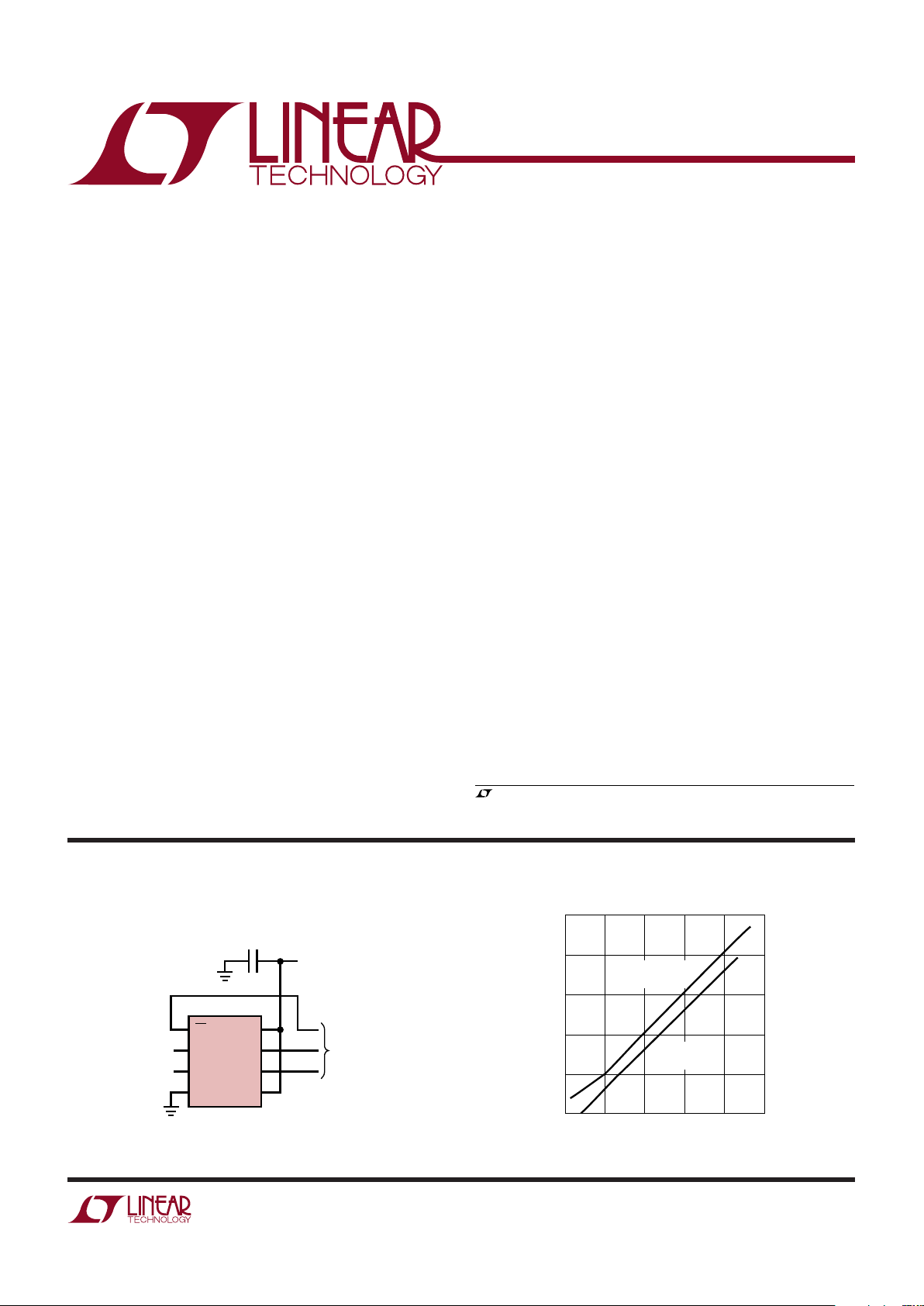
Supply Current vs Sampling Frequency
SAMPLING FREQUENCY (kHz)
0.01
SUPPLY CURRENT (µA)
100
1000
10000
100
1197/99 G03
10
1
0.1
0.1
1
10
1000
VCC = 5V
f
CLK
= 7.2MHz
VCC = 2.7V
f
CLK
= 3.5MHz
1
2
3
4
8
7
6
5
CS
+IN
–IN
GND
V
CC
CLK
D
OUT
V
REF
LTC1197L
1197/99 TA01
ANALOG INPUT
0V TO 2.7V RANGE
2.7V
1µF
SERIAL DATA LINK TO
ASIC, PLD, MPU, DSP
OR SHIFT REGISTERS
The LTC®1197/LTC1197L/LTC1199/LTC1199L are
10-bit A/D converters with sampling rates up to 500kHz.
They have 2.7V (L) and 5V versions and are offered in
8-pin MSOP and SO packages. Power dissipation is typically only 2.2mW at 2.7V (25mW at 5V) during full speed
operation. The automatic power down reduces supply
current linearly as sample rate is reduced. These 10-bit,
switched-capacitor, successive approximation ADCs include a sample-and-hold. The LTC1197/LTC1197L have a
differential analog input with an adjustable reference pin.
The LTC1199/LTC1199L offer a software-selectable
2-channel MUX.
The 3-wire serial I/O, MSOP and SO-8 packages, 2.7V
operation and extremely high sample rate-to-power ratio
make these ADCs ideal choices for compact, low power
high speed systems.
These circuits can be used in ratiometric applications or
with external references. The high impedance analog
inputs and the ability to operate with reduced spans below
1V full scale (LTC1197/LTC1197L) allow direct connection to signal sources in many applications, eliminating
the need for gain stages.
■
8-Pin MSOP and SO Packages
■
10-Bit Resolution at 500ksps
■
Single Supply: 5V or 3V
■
Low Power at Full Speed:
25mW Typ at 5V
2.2mW Typ at 2.7V
■
Auto Shutdown Reduces Power Linearly
at Lower Sample Rates
■
10-Bit Upgrade to 8-Bit LTC1196/LTC1198
■
SPI and MICROWIRETM Compatible Serial I/O
■
Low Cost
, LTC and LT are registered trademarks of Linear Technology Corporation.
MICROWIRE is a trademark of National Semiconductor Corporation.
■
High Speed Data Acquisition
■
Portable or Compact Instrumentation
■
Low Power or Battery-Operated Instrumentation
FEATURES
DESCRIPTIO
U
APPLICATIO S
U
TYPICAL APPLICATIO
U
2
LTC1197/LTC1197L
LTC1199/LTC1199L
Operating Temperature Range
LTC1197C/LTC1197LC
LTC1199C/LTC1199LC........................... 0°C to 70°C
LTC1197I/LTC1197LI
LTC1199I/LTC1199LI ........................ –45°C to 85°C
Lead Temperature (Soldering, 10 sec)................. 300°C
Supply Voltage (VCC) ............................................... 12V
Voltage
Analog Input ..................... GND – 0.3V to V
CC
+ 0.3V
Digital Input ................................ GND – 0.3V to 12V
Digital Output .................... GND – 0.3V to V
CC
+ 0.3V
Power Dissipation.............................................. 500mW
Storage Temperature Range .................– 65°C to 150°C
(Notes 1, 2)
LTC1197 LTC1199
SYMBOL PARAMETER CONDITIONS MIN TYP MAX MIN TYP MAX UNITS
V
CC
Supply Voltage 4 9 4 6 V
VCC = 5V Operation
f
CLK
Clock Frequency ● 0.05 7.2 0.05 7.2 MHz
t
CYC
Total Cycle Time 14 16 CLK
t
SMPL
Analog Input Sampling Time 1.5 1.5 CLK
t
hCS
Hold Time CS Low After Last CLK↑ 13 13 ns
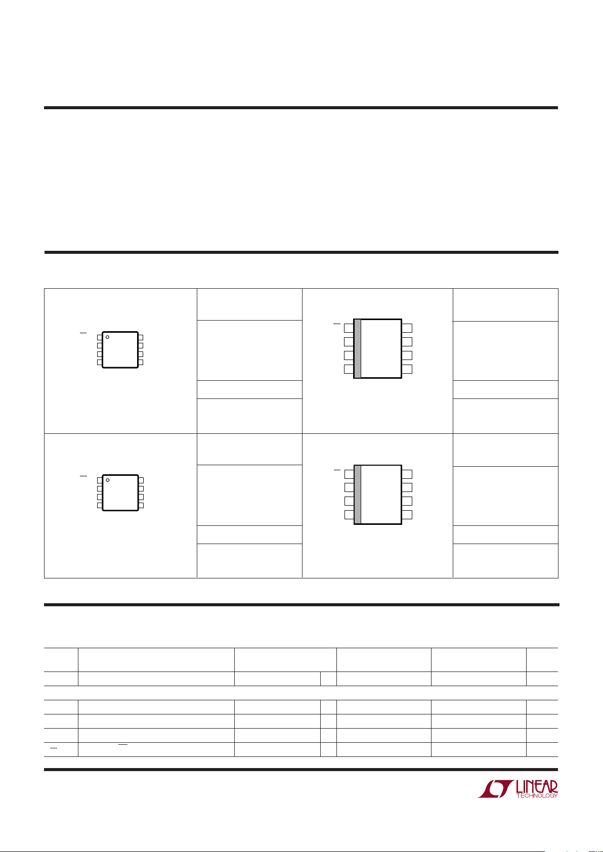
ORDER PART
NUMBER
MS8 PART MARKING S8 PART MARKING
1197L
1197LI
1197
1197I
LTC1197CS8
LTC1197IS8
LTC1197LCS8
LTC1197LIS8
ORDER PART
NUMBER
LTC1197CMS8
LTC1197IMS8
LTC1197LCMS8
LTC1197LIMS8
LTBL
LTJA
T
JMAX
= 150°C, θJA = 175°C/W
1
2
3
4
8
7
6
5
TOP VIEW
S8 PACKAGE
8-LEAD PLASTIC SO
CS
+IN
–IN
GND
V
CC
CLK
D
OUT
V
REF
ORDER PART
NUMBER
MS8 PART MARKING S8 PART MARKING
1199L
1199LI
1199
1199I
LTC1199CS8
LTC1199IS8
LTC1199LCS8
LTC1199LIS8
ORDER PART
NUMBER
LTC1199CMS8
LTC1199IMS8
LTC1199LCMS8
LTC1199LIMS8
LTCM
LTWC
T
JMAX
= 150°C, θJA = 210°C/W
1
2
3
4
CS
+IN
–IN
GND
8
7
6
5
V
CC
CLK
D
OUT
V
REF
TOP VIEW
MS8 PACKAGE
8-LEAD PLASTIC MSOP
1
2
3
4
CS
CH0
CH1
GND
8
7
6
5
V
CC
CLK
D
OUT
D
IN
TOP VIEW
MS8 PACKAGE
8-LEAD PLASTIC MSOP
T
JMAX
= 150°C, θJA = 210°C/W
T
JMAX
= 150°C, θJA = 175°C/W
1
2
3
4
8
7
6
5
TOP VIEW
S8 PACKAGE
8-LEAD PLASTIC SO
CS
CH0
CH1
GND
V
CC
CLK
D
OUT
D
IN
ABSOLUTE AXI U RATI GS
WWWU
PACKAGE/ORDER I FOR ATIO
UU
W
LTKV
LTKW
LTFL
LTWB
Consult factory for parts specified with wider operating temperature ranges.
RECO E DED OPERATI G CO DITIO S
UUUUWW
The ● denotes the specifications which apply over
the full operating temperature range, otherwise specifications are at TA = 25°C.
3
LTC1197/LTC1197L
LTC1199/LTC1199L
LTC1197 LTC1199
SYMBOL PARAMETER CONDITIONS MIN TYP MAX MIN TYP MAX UNITS
VCC = 5V Operation
t
suCS
Setup Time CS↓ Before First CLK↑ 26 26 ns
(See Figures 1, 2)
t
hDI
Hold Time DIN After CLK↑ LTC1199 26 ns
t
suDI
Setup Time DIN Stable Before CLK↑ LTC1199 26 ns
t
WHCLK
CLK High Time f
CLK
= f
CLK(MAX)
40% 40% 1/f
CLK
t
WLCLK
CLK Low Time f
CLK
= f
CLK(MAX)
40% 40% 1/f
CLK
t
WHCS
CS High Time Between Data Transfer Cycles 32 32 ns
t
WLCS
CS Low Time During Data Transfer 13 15 CLK
The ● denotes the specifications which apply over the full operating temperature range, otherwise specifications are at TA = 25°C.
VCC = 5V, V
REF
= 5V, f
CLK
= f
CLK(MAX)
as defined in Recommended Operating Conditions, unless otherwise noted.
–0.05V to VCC + 0.05V
LTC1197 LTC1199
PARAMETER CONDITIONS MIN TYP MAX MIN TYP MAX UNITS
Offset Error ● ±2 ±2 LSB
Linearity Error (Note 3) ● ±1 ±1 LSB
Gain Error ● ±4 ±4 LSB
No Missing Codes Resolution ● 10 10 Bits
Analog Input Range V
Reference Input Range LTC1197, VCC ≤ 6V 0.2 VCC + 0.05V V
LTC1197, V
CC
> 6V 0.2 6 V
Analog Input Leakage Current (Note 4) ● ±1 ±1 µA
LTC1197L LTC1199L
SYMBOL PARAMETER CONDITIONS MIN TYP MAX MIN TYP MAX UNITS
V
CC
Supply Voltage 2.7 4 2.7 4 V
VCC = 2.7V Operation
f
CLK
Clock Frequency ● 0.01 3.5 0.01 3.5 MHz
t
CYC
Total Cycle Time 14 16 CLK
t
SMPL
Analog Input Sampling Time 1.5 1.5 CLK
t
hCS
Hold Time CS Low After Last CLK↑ 40 40 ns
t
suCS
Setup Time CS↓ Before First CLK↑ 78 78 ns
(See Figures 1, 2)
t
hDI
Hold Time DIN After CLK↑ LTC1199L 78 ns
t
suDI
Setup Time DIN Stable Before CLK↑ LTC1199L 78 ns
t
WHCLK
CLK High Time f
CLK
= f
CLK(MAX)
40% 40% 1/f
CLK
t
WLCLK
CLK Low Time f
CLK
= f
CLK(MAX)
40% 40% 1/f
CLK
t
WHCS
CS High Time Between Data Transfer Cycles 96 96 ns
t
WLCS
CS Low Time During Data Transfer 13 15 CLK
The ● denotes the specifications which apply over
the full operating temperature range, otherwise specifications are at TA = 25°C.
RECO E DED OPERATI G CO DITIO S
UUUUWW
CO VERTER A D ULTIPLEXER CHARACTERISTICS
U
W
U
4
LTC1197/LTC1197L
LTC1199/LTC1199L
The ● denotes the specifications which apply over the full operating temperature range, otherwise specifications are at TA = 25°C.
VCC = 2.7V, V
REF
= 2.5V (LTC1197L), f
CLK
= f
CLK(MAX)
as defined in Recommended Operating Conditions, unless otherwise noted.
–0.05V to VCC + 0.05V
DYNAMIC ACCURACY
UW
VCC = 5V, V
REF
= 5V, f
CLK
= f
CLK(MAX)
as defined in Recommended Operating Conditions, unless otherwise noted.
LTC1197 LTC1199
SYMBOL PARAMETER CONDITIONS MIN TYP MAX MIN TYP MAX UNITS
S/(N + D) Signal-to-Noise Plus 100kHz Input Signal 60 60 dB
Distortion Ratio
THD Total Harmonic Distortion 100kHz Input Signal –64 –64 dB
First 5 Harmonics
Peak Harmonic or Spurious Noise 100kHz Input Signal –68 –68 dB
IMD Intermodulation Distortion f
IN1
= 97.046kHz, f
IN2
= 102.905kHz
2nd Order Terms –65 –65 dB
3rd Order Terms –70 –70 dB
VCC = 2.7V, V
REF
= 2.5V, f
CLK
= f
CLK(MAX)
as defined in Recommended Operating Conditions, unless otherwise noted.
LTC1197L LTC1199L
SYMBOL PARAMETER CONDITIONS MIN TYP MAX MIN TYP MAX UNITS
S/(N + D) Signal-to-Noise Plus 50kHz Input Signal 58 58 dB
Distortion Ratio
THD Total Harmonic Distortion 50kHz Input Signal –60 –60 dB
First 5 Harmonics
Peak Harmonic or Spurious Noise 50kHz Input Signal – 63 –63 dB
IMD Intermodulation Distortion f
IN1
= 48.5kHz, f
IN2
= 51.5kHz
2nd Order Terms –60 –60 dB
3rd Order Terms –65 –65 dB
LTC1197L LTC1199L
PARAMETER CONDITIONS MIN TYP MAX MIN TYP MAX UNITS
Offset Error ● ±2 ±2 LSB
Linearity Error (Note 3) ● ±1 ±1 LSB
Gain Error ● ±4 ±4 LSB
No Missing Codes Resolution ● 10 10 Bits
Analog Input Range V
Reference Input Range LTC1197L 0.2 VCC + 0.05V V
Analog Input Leakage Current (Note 4) ● ±1 ±1 µA
CO VERTER A D ULTIPLEXER CHARACTERISTICS
U
W
U
5
LTC1197/LTC1197L
LTC1199/LTC1199L
LTC1197 LTC1199
SYMBOL PARAMETER CONDITIONS MIN TYP MAX MIN TYP MAX UNITS
V
IH
High Level Input Voltage VCC = 5.25V ● 2.4 2.4 V
V
IL
Low Level Input Voltage VCC = 4.75V ● 0.8 0.8 V
I
IH
High Level Input Current VIN = V
CC
● 2.5 2.5 µA
I
IL
Low Level Input Current VIN = 0V ● –2.5 –2.5 µA
V
OH
High Level Output Voltage VCC = 4.75V, IO = 10µA ● 4.5 4.74 4.5 4.74 V
VCC = 4.75V, IO = 360µA ● 2.4 4.72 2.4 4.72 V
V
OL
Low Level Output Voltage VCC = 4.75V, IO = 1.6mA ● 0.4 0.4 V
I
OZ
Hi-Z Output Leakage CS = High ● ±3 ±3 µA
I
SOURCE
Output Source Current V
OUT
= 0V –25 –25 mA
I
SINK
Output Sink Current V
OUT
= V
CC
45 45 mA
I
REF
Reference Current (LTC1197) CS = V
CC
● 0.001 3 µA
f
SMPL
= f
SMPL(MAX)
● 0.5 1 mA
I
CC
Supply Current CS = V
CC
● 0.001 3 0.001 3 µA
f
SMPL
= f
SMPL(MAX)
● 4.5 8 5 8.5 mA
P
D
Power Dissipation f
SMPL
= f
SMPL(MAX)
22.5 25 mW
The ● denotes the specifications which apply
over the full operating temperature range, otherwise specifications are at TA = 25°C. VCC = 5V, V
REF
= 5V, unless otherwise noted.
DIGITAL AND DC ELECTRICAL CHARACTERISTICS
U
The ● denotes the specifications which apply over the full operating temperature range, otherwise specifications are at TA = 25°C.
VCC = 2.7V, V
REF
= 2.5V, unless otherwise noted.
LTC1197L LTC1199L
SYMBOL PARAMETER CONDITIONS MIN TYP MAX MIN TYP MAX UNITS
V
IH
High Level Input Voltage VCC = 3.6V ● 1.9 1.9 V
V
IL
Low Level Input Voltage VCC = 2.7V ● 0.45 0.45 V
I
IH
High Level Input Current VIN = V
CC
● 2.5 2.5 µA
I
IL
Low Level Input Current VIN = 0V ● –2.5 –2.5 µA
V
OH
High Level Output Voltage VCC = 2.7V, IO = 10µA ● 2.3 2.60 2.3 2.60 V
V
CC
= 2.7V, IO = 360µA ● 2.1 2.45 2.1 2.45 V
V
OL
Low Level Output Voltage VCC = 2.7V, IO = 400µA ● 0.3 0.3 V
I
OZ
Hi-Z Output Leakage CS = High ● ±3 ±3 µA
I
SOURCE
Output Source Current V
OUT
= 0V – 6.5 –6.5 mA
I
SINK
Output Sink Current V
OUT
= V
CC
11 11 mA
I
REF
Reference Current (LTC1197L) CS = V
CC
● 0.001 3.0 µA
f
SMPL
= f
SMPL(MAX)
● 0.250 0.5 mA
I
CC
Supply Current CS = V
CC
● 0.001 3 0.001 3 µA
f
SMPL
= f
SMPL(MAX)
● 0.8 2 0.8 2 mA
P
D
Power Dissipation f
SMPL
= f
SMPL(MAX)
2.2 2.2 mW

6
LTC1197/LTC1197L
LTC1199/LTC1199L
AC CHARACTERISTICS
The ● denotes the specifications which apply over the full operating temperature range, otherwise specifications are at TA = 25°C.
VCC = 5V, V
REF
= 5V, f
CLK
= f
CLK(MAX)
as defined in Recommended Operating Conditions, unless otherwise noted.
LTC1197 LTC1199
SYMBOL PARAMETER CONDITIONS MIN TYP MAX MIN TYP MAX UNITS
t
CONV
Conversion Time (See Figures 1, 2) ● 1.4 1.4 µs
f
SMPL(MAX)
Maximum Sampling Frequency ● 500 450 kHz
t
dDO
Delay Time, CLK↑ to D
OUT
Data Valid C
LOAD
= 20pF 68 78 68 78 ns
● 100 100 ns
t
dis
Delay Time, CS↑ to D
OUT
Hi-Z ● 75 150 75 150 ns
t
en
Delay Time, CLK↓ to D
OUT
Enabled C
LOAD
= 20pF ● 40 68 40 68 ns
t
hDO
Time Output Data Remains C
LOAD
= 20pF ● 15 55 15 55 ns
Valid After CLK↑
t
r
D
OUT
Rise Time C
LOAD
= 20pF ● 10 20 10 20 ns
t
f
D
OUT
Fall Time C
LOAD
= 20pF ● 10 20 10 20 ns
C
IN
Input Capacitance Analog Input On Channel 20 20 pF
Analog Input Off Channel 5 5 pF
Digital Input 5 5 pF
LTC1197L LTC1199L
SYMBOL PARAMETER CONDITIONS MIN TYP MAX MIN TYP MAX UNITS
t
CONV
Conversion Time (See Figures 1, 2) ● 2.9 2.9 µs
f
SMPL(MAX)
Maximum Sampling Frequency ● 250 210 kHz
t
dDO
Delay Time, CLK↑ to D
OUT
Data Valid C
LOAD
= 20pF 130 180 130 180 ns
● 250 250 ns
t
dis
Delay Time, CS↑ to D
OUT
Hi-Z ● 120 250 120 250 ns
t
en
Delay Time, CLK↓ to D
OUT
Enabled C
LOAD
= 20pF ● 100 200 100 200 ns
t
hDO
Time Output Data Remains C
LOAD
= 20pF ● 30 120 30 120 ns
Valid After CLK↑
t
r
D
OUT
Rise Time C
LOAD
= 20pF ● 15 40 15 40 ns
t
f
D
OUT
Fall Time C
LOAD
= 20pF ● 15 40 15 40 ns
C
IN
Input Capacitance Analog Input On Channel 20 20 pF
Analog Input Off Channel 5 5 pF
Digital Input 5 5 pF
The ● denotes the specifications which apply over the full operating temperature range, otherwise specifications are at TA = 25°C.
VCC = 2.7V, V
REF
= 2.5V, f
CLK
= f
CLK(MAX)
as defined in Recommended Operating Conditions, unless otherwise noted.
Note 1: Absolute Maximum Ratings are those values beyond which the life
of a device may be impaired.
Note 2: All voltage values are with respect to GND.
Note 3: Integral nonlinearity is defined as deviation of a code from a
straight line passing through the actual endpoints of the transfer curve.
The deviation is measured from the center of the quantization band.
Note 4: Channel leakage current is measured after the channel selection.
7
LTC1197/LTC1197L
LTC1199/LTC1199L
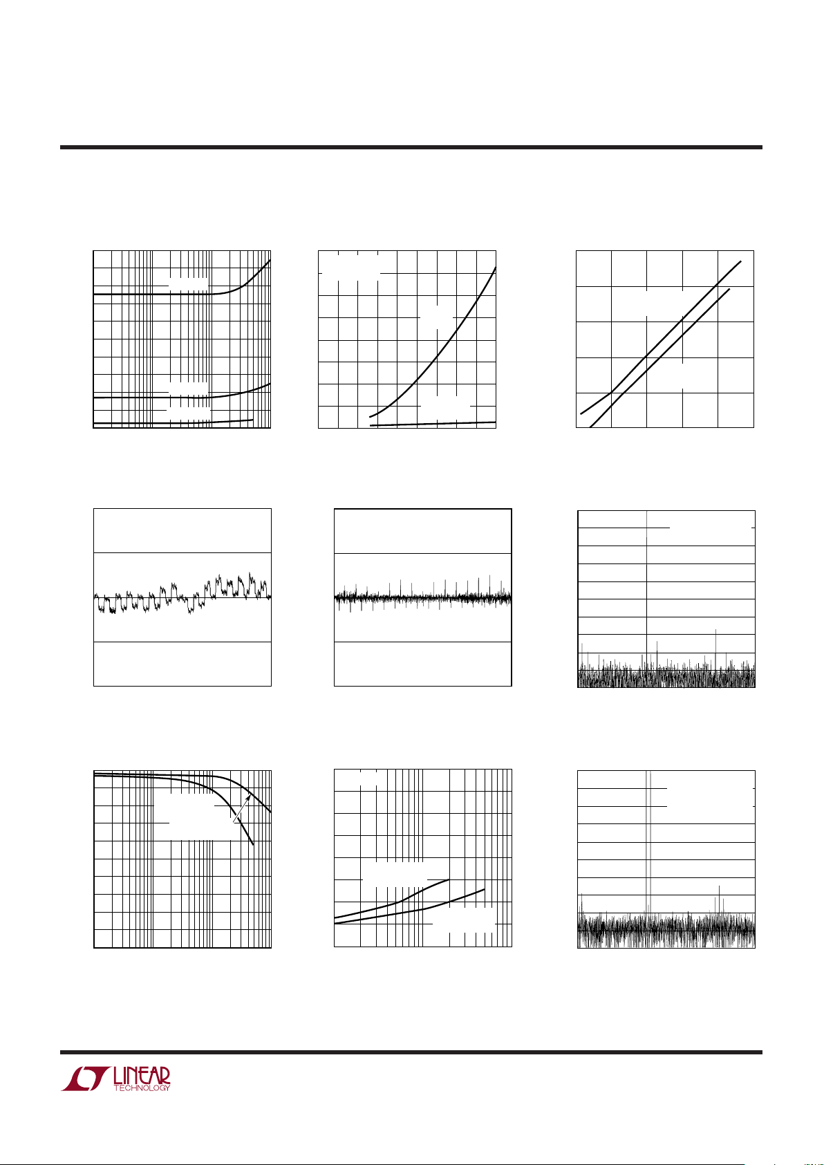
Supply Current
vs Sampling Frequency
Supply Current vs Clock Rate*
FREQUENCY (kHz)
10
8
SUPPLY CURRENT (mA)
10
12
14
16
100 1000 10000
1197/99 G01
6
4
2
0
18
20
VCC = 9V
VCC = 5V
VCC = 2.7V
SAMPLING FREQUENCY (kHz)
0.01
SUPPLY CURRENT (µA)
100
1000
10000
100
1197/99 G03
10
1
0.1
0.1
1
10
1000
VCC = 5V
f
CLK
= 7.2MHz
VCC = 2.7V
f
CLK
= 3.5MHz
Supply Current vs Supply Voltage
SUPPLY VOLTAGE (V)
10
SUPPLY CURRENT (mA)
SHUTDOWN CURRENT (nA)
8
10
12
56789
1197/99 G02
6
4
0
2
3
4
2
16
14
40
50
60
30
20
0
10
80
70
SHUTDOWN
MODE
ACTIVE
MODE
f
CLK
= 3.5MHz
T
A
= 25°C
CODE
0
–1.0
INL (LSBs)
–0.5
0
0.5
1.0
128 256 384 512
1197/99 G04
640 768 896 1024
VCC = V
REF
= 5V
f
CLK
= 7.2MHz
T
A
= 25°C
INL Plot
FREQUENCY (kHz)
0
AMPLITUDE (dB)
–40
–20
–30
–10
0
1197/99 G06
–60
–80
–50
–70
–90
–100
50
100 150 200 250
f
SMPL
= 500kHz
f
IN
= 97.045898kHz
LTC1197 4096 Point FFT
FREQUENCY (kHz)
1
4
ENOBs
5
6
7
8
10 100 1000
1197/99 G07
3
2
1
0
9
10
VCC = 2.7V
f
SMPL
= 250kHz
VCC = 5V
f
SMPL
= 500kHz
ENOBs vs Frequency Intermodulation Distortion Plot
*Part is continuously sampling, spending only a minimum amount of time in shutdown.
FREQUENCY (kHz)
0
AMPLITUDE (dB)
–20
–30
–40
–50
–60
–70
–80
–90
–100
–10
0
1197/99 G09
50
100 150 200 250
f
SMPL
= 500kHz
f
IN1
= 97.045898kHz
f
IN2
= 102.905273kHz
CODE
0
–1.0
DNL (LSBs)
–0.5
0
0.5
1.0
128 256 384 512
1197/99 G26
640 768 896 1024
VCC = V
REF
= 5V
f
CLK
= 7.2MHz
T
A
= 25°C
DNL Plot
THD vs Frequency
FREQUENCY (kHz)
10
THD (dB)
0
100 1000
1197/99 G08
–10
–20
–30
–40
–50
–60
–70
–80
TA = 25°C
V
CC
= 2.7V
f
SMPL
= 250kHz
VCC = 5V
f
SMPL
= 500kHz
TYPICAL PERFOR A CE CHARACTERISTICS
UW
8
LTC1197/LTC1197L
LTC1199/LTC1199L
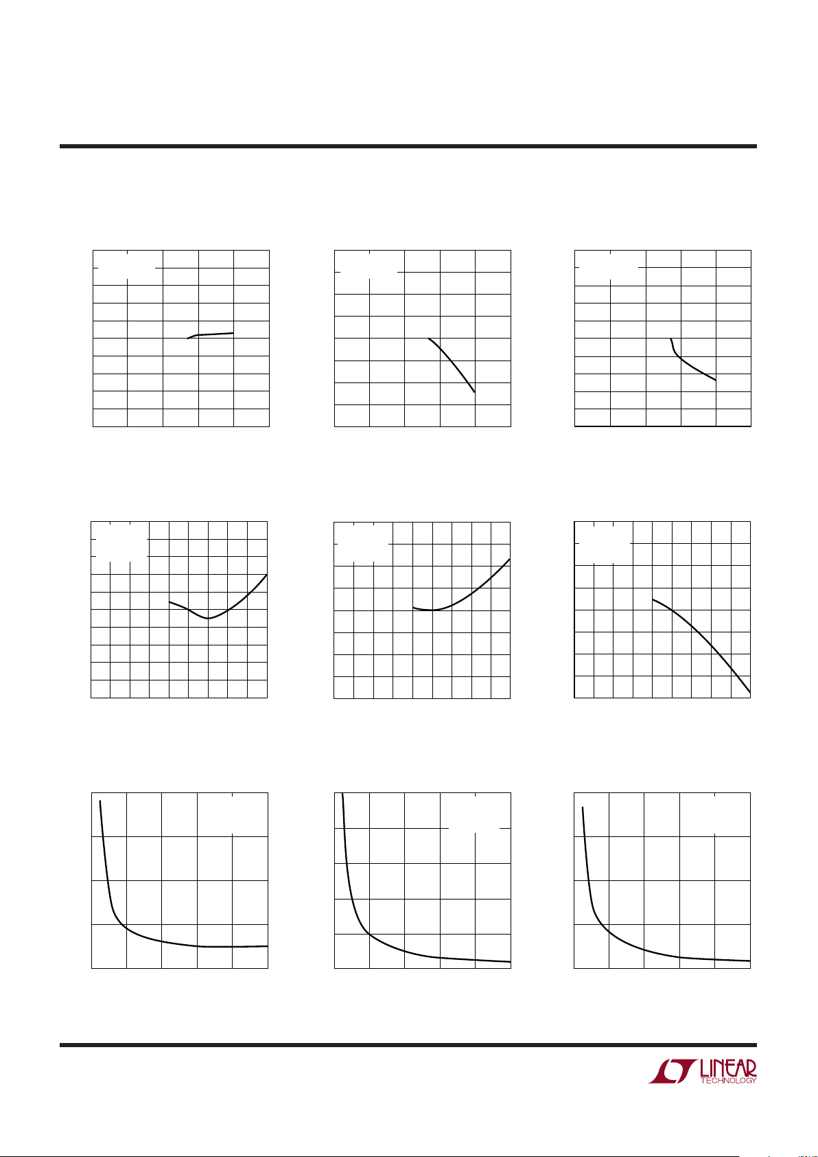
LTC1197L Change in Gain Error
vs Supply Voltage
LTC1197L Change in Offset
vs Supply Voltage
SUPPLY VOLTAGE (V)
0
CHANGE IN LINEARITY (LSBs)
0
0.6
1.0
4
1197/99 G10
–0.4
–0.8
0.4
0.2
0.8
–0.2
–0.6
–1.0
1
2
3
5
V
REF
= 2.5V
f
CLK
= 3.5MHz
LTC1197L Change in Linearity
vs Supply Voltage
SUPPLY VOLTAGE (V)
0
CHANGE IN OFFSET (LSBs)
–0.5
0
0.5
1.0
1.5
2.0
4
1197/99 G11
–1.0
–1.5
–2.0
1
2
3
5
V
REF
= 2.5V
f
CLK
= 3.5MHz
SUPPLY VOLTAGE (V)
0
CHANGE IN GAIN ERROR (LSBs)
0.2
0.6
1.0
4
1197/99 G12
–0.2
–0.6
0
0.4
0.8
–0.4
–0.8
–1.0
1
2
3
5
V
REF
= 2.5V
f
CLK
= 3.5MHz
LTC1197 Offset Error
vs Reference Voltage
LTC1197 Gain Error
vs Reference Voltage
LTC1197 Change in Linearity
vs Supply Voltage
SUPPLY VOLTAGE (V)
0
–1.0
CHANGE IN LINEARITY (LSBs)
–0.8
–0.4
–0.2
0
1.0
0.4
2
4
59
1197/99 G13
–0.6
0.6
0.8
0.2
13
6
7
8
V
REF
= 4V
f
CLK
= 7MHz
T
A
= 25°C
LTC1197 Change in Offset
vs Supply Voltage
SUPPLY VOLTAGE (V)
0
–2.0
CHANGE IN OFFSET (LSBs)
1.5
2.0
1.0
0.5
0
–0.5
–1.0
–1.5
1197/99 G14
123456789
V
REF
= 4V
f
CLK
= 7MHz
T
A
= 25°C
LTC1197 Change in Gain Error
vs Supply Voltage
SUPPLY VOLTAGE (V)
0
CHANGE IN GAIN ERROR (LSBs)
–2.0
1.0
0.5
0
1.5
2.0
2
4
59
1197/99 G15
–1.5
–1.0
–0.5
13
6
7
8
V
REF
= 4V
f
CLK
= 7MHz
T
A
= 25°C
LTC1197 Linearity Error
vs Reference Voltage
REFERENCE VOLTAGE (V)
0
LINEARITY ERROR (LSBs)
1.0
1.5
4
1197/99 F16
0.5
0
1
2
3
5
2.0
VCC = 5V
f
CLK
= 7.2MHz
T
A
= 25°C
REFERENCE VOLTAGE (V)
0
OFFSET ERROR (LSBs)
1.5
2.0
2.5
4
1197/99 G17
1.0
0.5
0
1
2
3
5
VCC = 5V
f
CLK
= 7.2MHz
T
A
= 25°C
REFERENCE VOLTAGE (V)
0
GAIN ERROR (LSBs)
1.0
1.5
4
1197/99 F18
0.5
0
1
2
3
5
2.0
VCC = 5V
f
CLK
= 7.2MHz
T
A
= 25°C
TYPICAL PERFOR A CE CHARACTERISTICS
UW
9
LTC1197/LTC1197L
LTC1199/LTC1199L
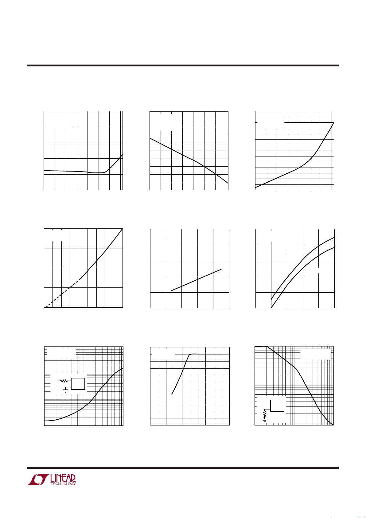
Linearity vs Temperature
TEMPERATURE (°C)
–55 –30
0
LINEARITY ERROR (LSBs)
0.2
0.5
–5 45 70
1197/99 G19
0.1
0.4
0.3
20 95 120
VCC = 5V
V
REF
= 5V
f
CLK
= 7.2MHz
Gain Error vs Temperature
TEMPERATURE (°C)
–55 –30
–1.0
–1.2
–1.4
GAIN ERROR (LSBs)
0
–5 45 70
1197/99 G21
–0.2
–0.4
–0.6
–0.8
20 95 120
VCC = 5V
V
REF
= 5V
f
CLK
= 7.2MHz
Offset vs Temperature
TEMPERATURE (°C)
–55 –30
–1.0
OFFSET VOLTAGE (LSBs)
0
–5 45 70
1197/99 G20
–0.2
–0.3
–0.4
–0.5
–0.6
–0.7
–0.8
–0.9
–0.1
20 95 120
VCC = 5V
V
REF
= 5V
f
CLK
= 7.2MHz
*As the CLK frequency is decreased from 2MHz, minimum CLK frequency (∆error ≤ 0.1LSB)
represents the frequency at which a 0.1LSB shift in any code translation from its 2MHz value
is first detected.
†
Maximum CLK frequency represents the clock frequency at which a 0.1LSB shift in the error
at any code transition from its 3.5MHz value is first detected.
Acquisition Time
vs Source Resistance
Maximum Clock Frequency
vs Supply Voltage
Maximum Clock Frequency
†
vs Source Resistance
SOURCE RESISTANCE (Ω)
100 1000
0.1
ACQUISITION TIME (µs)
1
10
100
10000
1197/99 G25
VCC = V
REF
= 5V
T
A
= 25°C
+INPUT
R
SOURCE
+
V
IN
COM
SUPPLY VOLTAGE (V)
0
MAXIMUM CLOCK FREQUENCY (MHz)
6
8
10
11
8
1197/99 G26
4
2
5
7
9
3
1
0
2
4
6
19
3
5
7
10
V
REF
= 2.5V
T
A
= 25°C
SOURCE RESISTANCE (Ω)
100
100
MAXIMUM CLOCK FREQUENCY (kHz)
1000
10000
1000 10000
1197/99 G27
V
REF
= V
CC =
5V
T
A
= 25°C
+INPUT
R
SOURCE
–
V
IN
–INPUT
TEMPERATURE (°C)
–55
0.1
MINIMUM CLOCK FREQUENCY (kHz)
1
10
100
1000
–35 –15 5 25
1197/99 G22
45 65 85 105 125
V
REF
= 5V
V
CC
= 5V
Minimum Clock Frequency for
0.1LSB Error* vs Temperature
Digital Input Threshold
vs Supply Voltage
Input Channel Leakage Current
vs Temperature
SUPPLY VOLTAGE (V)
0
LOGIC THRESHOLD (V)
3
4
5
8
1197/99 G23
2
1
0
2
4
6
10
TA = 25°C
TEMPERATURE (°C)
0
LEAKAGE CURRENT (nA)
1
10
100
100
1197/99 G24
0.1
0.01
0.001
25
50
75
125
V
REF
= 5V
V
CC
= 5V
ON CHANNEL
OFF CHANNEL
TYPICAL PERFOR A CE CHARACTERISTICS
UW
 Loading...