

Linear Technology LTC1174CN8-5, LTC1174CN8-3.3, LTC1174CN8, LTC1174IS8, LTC1174HVCS8-3.3 Datasheet
...
FEATURES
LOAD CURRENT (mA)
1
EFFICIENCY (%)
100
95
90
85
80
75
70
10 100
1174 TA02
200
VIN = 6V
V
IN
= 9V
L = 100µH
V
OUT
= 5V
I
PGM
= 0V
■
High Efficiency: Up to 94%
■
Peak Inductor Current Independent of
Inductor Value
■
Short-Circuit Protection
■
Optimized for 5V to –5V Applications
■
Wide VIN Range: 4V to 18.5V
■
Low Dropout Operation
■
Low-Battery Detector
■
Pin Selectable Current Limit
■
Internal 0.9Ω Power Switch: VIN = 9V
■
Only Four External Components Required
■
130µA Standby Current
■
Active Low Micropower Shutdown
U
APPLICATIO S
■
Distributed Power Systems
■
Step-Down Converters
■
Inverting Converters
■
Memory Backup Supply
■
Portable Instruments
■
Battery-Powered Equipment
LTC1174
LTC1174-3.3/LTC1174-5
High Efficiency
Step-Down and Inverting
DC/DC Converter
U
DESCRIPTIO
The LTC®1174 is a simple current mode DC/DC converter
ideally suited for 9V to 5V, 5V to 3.3V or 5V to –5V
operation. With an internal 0.9Ω switch (at a supply
voltage of 9V), the LTC1174 requires only four external
components to construct a complete high efficiency
DC/DC converter.
Under a no load condition the LTC1174 draws only 130µA.
In shutdown, it draws a mere 1µA making this converter
ideal for current sensitive applications. In dropout, the
internal P-channel MOSFET switch is turned on continuously allowing the user to maximize the life of the battery
source.
The maximum inductor current of the LTC1174 family is
pin selectable to either 340mA or 600mA, optimizing
efficiency for a wide range of applications. Operation up to
200kHz permits the use of small surface mount inductors
and capacitors.
For applications requiring higher output current or ultrahigh efficiency, see the LTC1148 data sheet.
and LTC are registered trademarks and LT is a trademark of Linear Technology Corporation.
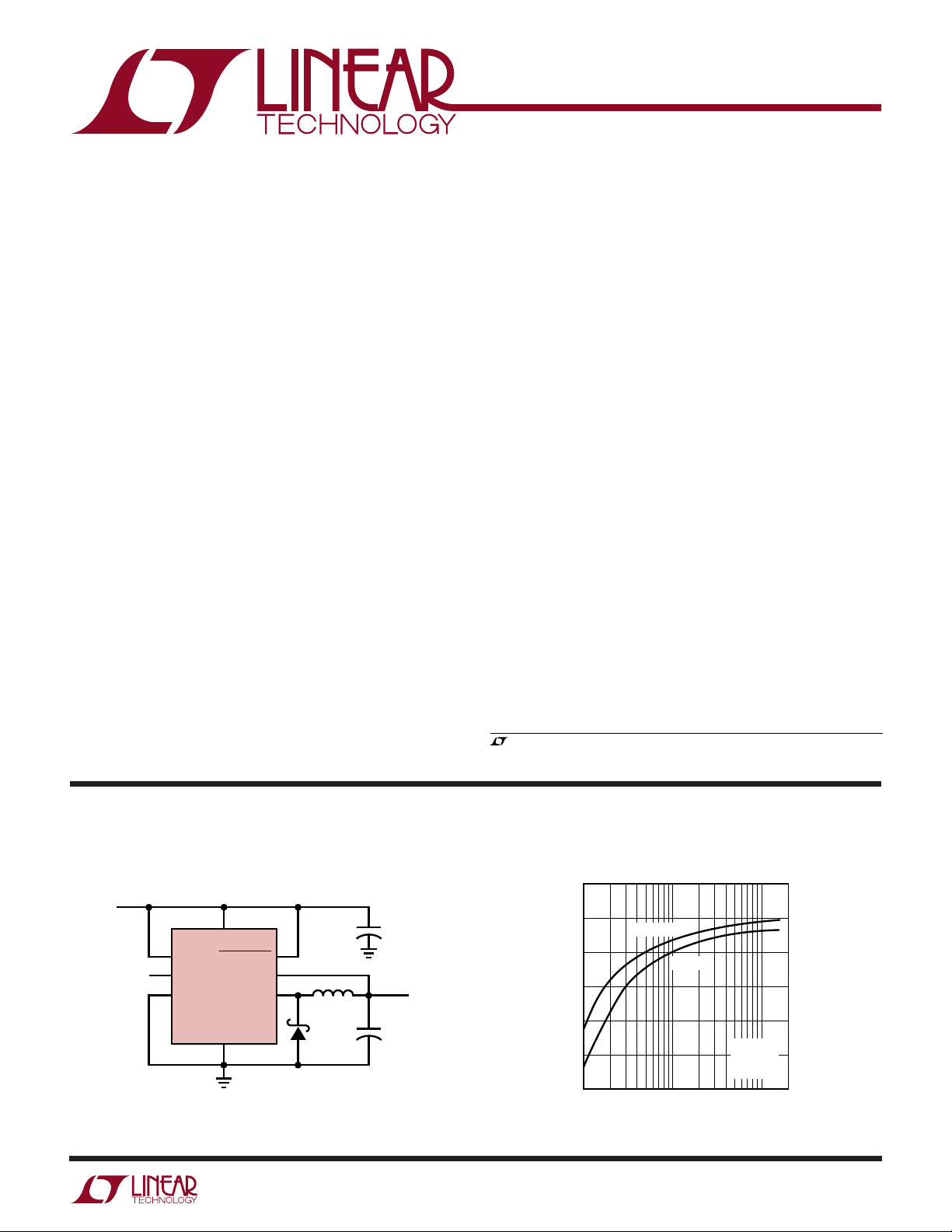
TYPICAL APPLICATIO
High Efficiency Step-Down Converter
V
IN
9V
3
2
7
(3) AVX TPSD156K025
*
AVX TPSD107K010
**
†
COILTRONICS CTX100-4
LB
LB
I
PGM
V
SHUTDOWN
IN
OUT
LTC1174-5
GND
6
IN
4
8
1
V
OUT
5
SW
U
100µH
1N5818
LTC1174-5 Efficiency
15µF*
+
25V
×3
†
+
5V
175mA
100µF**
10V
1174 TA01
1
LTC1174
LTC1174-3.3/LTC1174-5
WWWU
ABSOLUTE AXI U RATI GS
(Note 1)
(Voltage Referred to GND Pin)
Input Supply Voltage (Pin 6)
LTC1174........................................... –0.3V to 13.5V
LTC1174HV ...................................... –0.3V to 18.5V
Switch Current (Pin 5) .............................................. 1A
Switch Voltage (Pin 5)
LTC1174................................................. VIN – 13.5V
LTC1174HV ............................................ VIN – 18.5V
UU
W
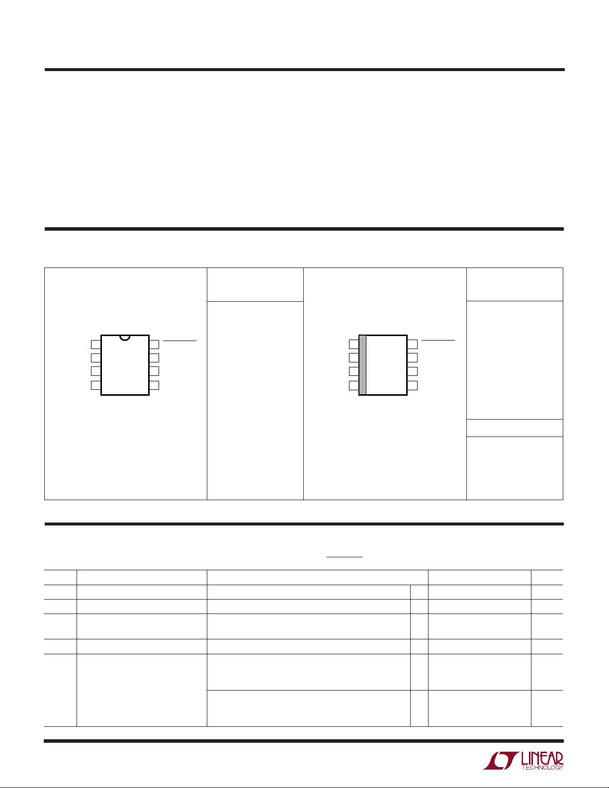
PACKAGE/ORDER I FOR ATIO
ORDER PART
NUMBER
LTC1174CN8
TOP VIEW
(VFB*)
V
OUT
1
LB
2
OUT
LB
3
IN
GND
4
N8 PACKAGE
8-LEAD PDIP
* ADJUSTABLE OUTPUT VERSION
T
= 125°C, θJA = 110°C/W
JMAX
SHUTDOWN
8
I
7
PGM
V
6
IN
SW
5
LTC1174CN8-3.3
LTC1174CN8-5
LTC1174IN8
LTC1174HVCN8
LTC1174HVCN8-3.3
LTC1174HVCN8-5
Operating Temperature Range
LTC1174CX ............................................ 0°C to 70°C
LTC1174IX ........................................ –40°C to 85°C
Junction Temperature (Note 2)............................ 125°C
Storage Temperature Range ................ –65°C to 150°C
Lead Temperature (Soldering, 10 sec)................. 300°C
ORDER PART
NUMBER
LTC1174CS8
TOP VIEW
V
(VFB*)
OUT
1
LB
2
OUT
LB
3
IN
GND
4
S8 PACKAGE
8-LEAD PLASTIC SO
* ADJUSTABLE OUTPUT VERSION
T
= 125°C, θJA = 150°C/W
JMAX
SHUTDOWN
8
I
7
PGM
V
6
IN
SW
5
LTC1174CS8-3.3
LTC1174CS8-5
LTC1174IS8
LTC1174HVCS8
LTC1174HVCS8-3.3
LTC1174HVCS8-5
LTC1174HVIS8
S8 PART MARKING
1174
117433
117450
1174I
1174HV
1174H3
1174H5
1174HI
Consult factor for Military grade parts.
ELECTRICAL CHARACTERISTICS
temperature range, otherwise specifications are at TA = 25°C. VIN = 9V, V
SYMBOL PARAMETER CONDITIONS MIN TYP MAX UNITS
I
V
V
∆V
FB
FB
OUT
Feedback Current LTC1174/LTC1174HV 1 µA
Feedback Voltage LTC1174/LTC1174HV ● 1.20 1.25 1.30 V
Regulated Output Voltage LTC1174-3.3/LTC1174HV-3.3 ● 3.14 3.30 3.46 V
LTC1174-5/LTC1174V-5
Output Voltage Line Regulation VIN = 6V to 12V, I
OUT
Output Voltage Load Regulation LTC1174-3.3 (Note 3)
20mA < I
20mA < I
LTC1174-5 (Note 3)
20mA < I
20mA < I
The ● denotes specifications which apply over the full operating
LOAD
< 175mA, I
LOAD
< 400mA, I
LOAD
< 175mA, I
LOAD
< 400mA, I
LOAD
= 100mA, I
PGM
PGM
PGM
PGM
SHUTDOWN
PGM
= 0V –5 –70 mV
= V
= 0V –5 –70 mV
= V
= VIN, I
= VIN (Note 3) 10 70 mV
IN
IN
= 0V, unless otherwise noted.
PGM
● 4.75 5.00 5.25 V
–45 –70 mV
–50 –70 mV
2
LTC1174
LTC1174-3.3/LTC1174-5
ELECTRICAL CHARACTERISTICS
temperature range, otherwise specifications are at TA = 25°C. VIN = 9V, V
The ● denotes specifications which apply over the full operating
SHUTDOWN
= VIN, I
= 0V, unless otherwise noted.
PGM
SYMBOL PARAMETER CONDITIONS MIN TYP MAX UNITS
I
Q
Input DC Supply Current (Note 4) Active Mode
LTC1174: 4V < V
LTC1174HV: 4V < VIN < 16V, I
< 12V, I
IN
= 0V 450 600 µA
PGM
= 0V 450 600 µA
PGM
Sleep Mode
LTC1174: 4V < V
< 12V 130 180 µA
IN
LTC1174HV: 4V < VIN < 16V 130 180 µA
SHUTDOWN (Note 4)
= 0V, 4V < VIN < 12V 1 10 µA
SHUTDOWN
= 0V, 4V < VIN < 16V 2 25 µA
= 0.4V 1.0 1.2 1.5 mA
= 0.4V 0.6 0.8 1.5 mA
LBOUT
= 0V ● 0.54 0.60 0.78 A
OUT
= 0V ● 0.27 0.34 0.50 A
V
LBTRIP
I
LBIN
I
LBOUT
V
HYST
I
PEAK
R
ON
LTC1174: V
SHUTDOWN
LTC1174HV: V
Low-Battery Trip Point 1.25 1.4 V
Current into Pin 3 0.5 µA
Current Sunk by Pin 2 LTC1174: V
LBOUT
LTC1174HV: V
Comparator Hysteresis LTC1174/LTC1174HV 7.5 15 30 mV
Current Limit I
PGM
I
PGM
= VIN, V
= 0V, V
OUT
ON Resistance of Switch LTC1174 ● 0.75 1.30 Ω
LTC1174HV ● 0.90 1.55 Ω
t
V
V
I
I
OFF
IH
IL
IH
IL
Switch Off-Time (Note 6) V
at Regulated Value 3 4 5 µs
OUT
SHUTDOWN Pin High Minimum Voltage at Pin 8 for Device to Be Active 1.2 V
SHUTDOWN Pin Low Maximum Voltage at Pin 8 for Device to Be in Shutdown 0.75 V
SHUTDOWN Pin Input Current LTC1174: V
LTC1174HV: V
SHUTDOWN Pin Input Current 0 ≤ V
SHUTDOWN
SHUTDOWN
= 12V 0.5 µA
SHUTDOWN
= 16V 2.0 µA
≤ 0.8V 0.5 µA
The ● denotes specifications which apply over the full operating temperature range,
otherwise specifications are at –40°C ≤ TA ≤ 85°C. LTC1174I and LTC1174HVI Only.
SYMBOL PARAMETER CONDITIONS MIN TYP MAX UNITS
V
FB
I
LBOUT
I
PEAK
t
OFF
R
ON
Note 1: Absolute Maximum Ratings are those values beyond which the life
of a device may be impaired.
Note 2: T
dissipation P
Feedback Voltage LTC1174I/LTC1174HVI ● 1.18 1.25 1.31 V
Current Sunk by Pin 2 V
Current Limit I
Switch Off-Time (Note 6) V
= 0.4V (LTC1174I) ● 0.75 1.2 2.0 mA
LBOUT
V
= 0.4V (LTC1174HVI) ● 0.50 0.8 1.6 mA
LBOUT
= VIN, V
PGM
I
= 0V, V
PGM
I
= VIN, V
PGM
I
= 0V, V
PGM
at Regulated Value (LTC1174I) ● 2.0 4 6.0 µs
OUT
V
at Regulated Value (LTC1174HVI) ● 1.8 4 6.2 µs
OUT
= 0V (LTC1174I) ● 0.54 0.60 0.78 A
OUT
= 0V (LTC1174I) 0.34 A
OUT
= 0V (LTC1174HVI) ● 0.5 0.60 0.8 A
OUT
= 0V (LTC1174HVI) 0.34 A
OUT
Switch On Resistance LTC1174I/LTC1174HVI ● 0.9 1.7 Ω
Note 3: Guaranteed by design.
Note 4: Dynamic supply current is higher due to the gate charge being
is calculated from the ambient temperature TA and power
J
according to the following formulas:
D
LTC1174CN8, LTC1174CN8-3.3, LTC1174CN8-5:
= TA + (PD × 110°C/W)
T
J
delivered at the switching frequency.
Note 5: Current into Pin 6 only, measured without electrolytic input
capacitor.
Note 6: The off-time is wafer-sort trimmed.
LTC1174CS8, LTC1174CS8-3.3, LTC1174CS8-5:
= TA + (PD × 150°C/W)
T
J
3
LTC1174
LTC1174-3.3/LTC1174-5
UW
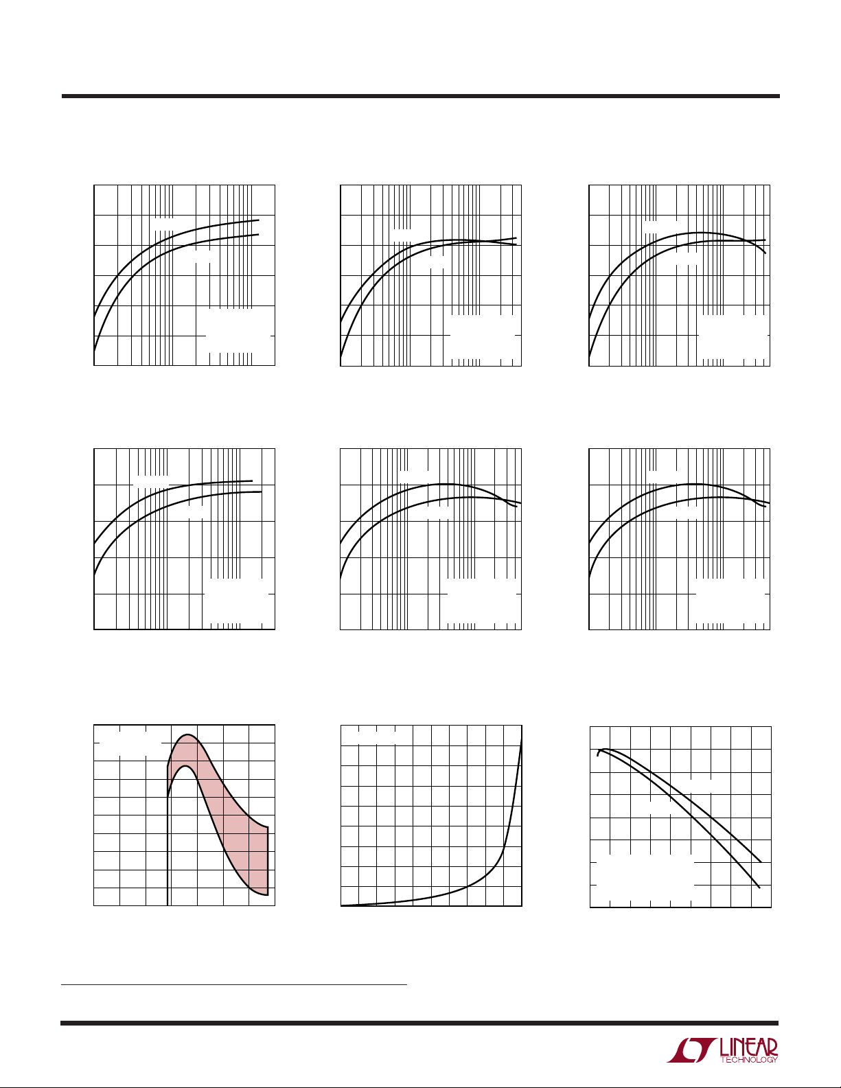
TYPICAL PERFOR A CE CHARACTERISTICS
Efficiency vs Load Current Efficiency vs Load Current Efficiency vs Load Current
100
100
100
95
90
85
EFFICIENCY (%)
80
75
70
1
100
90
80
70
EFFICIENCY (%)
60
50
1
VIN = 6V
= 9V
V
IN
10 100
LOAD CURRENT (mA)
VIN = 5V
VIN = 9V
10 100
LOAD CURRENT (mA)
L = 50µH
V
= 5V
OUT
= 0V
I
PGM
COIL = CTX50-4
1174 G01
L = 50µH
V
= 3.3V
OUT
= 0V
I
PGM
COIL = CTX50-4
1174 G04
200
300
95
90
85
EFFICIENCY (%)
80
75
70
1
100
90
80
70
EFFICIENCY (%)
60
50
1
VIN = 6V
VIN = 9V
L = 50µH
V
OUT
I
PGM
COIL = CTX50-4
10 100
LOAD CURRENT (mA)
VIN = 5V
VIN = 9V
L = 100µH
V
OUT
I
PGM
COIL = CTX100-4
10 100
LOAD CURRENT (mA)
= 5V
= V
= 3.3V
= V
IN
IN
1174 G02
1174 G06
400
500
95
90
85
EFFICIENCY (%)
80
75
70
1
Efficiency vs Load CurrentEfficiency vs Load Current Efficiency vs Load Current
100
90
80
70
EFFICIENCY (%)
60
50
1
VIN = 6V
VIN = 9V
L = 100µH
V
OUT
I
PGM
COIL = CTX100-4
10 100
LOAD CURRENT (mA)
VIN = 5V
VIN = 9V
L = 100µH
V
OUT
I
PGM
COIL = CTX100-4
10 100
LOAD CURRENT (mA)
= 5V
= V
= 3.3V
= V
IN
IN
500
1174 G03
500
1174 G06
Line Regulation
6
I
= 100mA
LOAD
4
= 0V
I
PGM
2
0
–2
(mV)
–4
OUT
–6
∆V
–8
–10
–12
–14
0
Kool Mµ is a registered trademark of Magnetics, Inc.
4
2
INPUT VOLTAGE (V)
8
6
10
12
4
1174 G07
Switch Leakage Current
vs Temperature Efficiency vs Input Voltage
180
VIN = 13.5V
160
140
120
100
80
60
LEAKAGE CURRENT (nA)
40
20
14
0
0
40
20 60
TEMPERATURE (°C)
100
80
1174 G08
95
94
93
92
91
90
EFFICIENCY (%)
V
89
OUT
I
PGM
I
88
LOAD
CORE = CTX (Kool Mµ
87
5
68
L = 50µH
= 5V
= 0V
= 75mA
7
INPUT VOLTAGE (V)
L = 100µH
®
)
9
10 11 13
14
12
1174 G09
LTC1174-3.3/LTC1174-5
INPUT VOLTAGE (V)
0
SUPPLY CURRENT (µA)
500
450
400
350
300
250
200
150
100
50
0
4
8
10
1174 G12
2
6
12
14
ACTIVE MODE
I
PGM
= V
IN
SLEEP MODE
I
PGM
= 0V
TA = 25°C
UW
TYPICAL PERFOR A CE CHARACTERISTICS
LTC1174
Efficiency vs Input Voltage
95
94
93
92
I
= 300mA
LOAD
= V
I
PGM
EFFICIENCY (%)
91
90
89
68
5
IN
7
9
INPUT VOLTAGE (V)
Operating Frequency
vs VIN – V
2.0
V
1.5
1.0
0.5
NORMALIZED FREQUENCY
0
0
OUT
OUT
= 5V
TA = 25°C
3
2
1
(VIN – V
4
OUT
V
= 5V
OUT
L = 100µH
COIL = CTX100-4
I
= 100mA
LOAD
= 0V
I
PGM
12
10 14
11
TA = 70°C
57
6
) VOLTAGE (V)
13
1174 G10
8
1174 G13
Supply Current in Shutdown
1.8
SHUTDOWN = 0V
1.6
T
= 25°C
A
CURRENT INTO PIN 6 ONLY
1.4
1.2
1.0
0.8
0.6
SUPPLY CURRENT (µA)
0.4
0.2
0
0
2
6
414
INPUT VOLTAGE (V)
8
10 12
1174 G11
DC Supply Current
Switch Resistance vs
Input Voltage
1.7
1.6
1.5
1.4
1.3
(Ω)
1.2
(ON)
1.1
RDS
1.0
0.9
0.8
9
0.7
4
LTC1174
6
8
INPUT VOLTAGE (V)
LTC1174HV
10
12
TA = 25°C
14 16 18 20
1174 G14
Off-Time vs Output Voltage
50
40
30
20
OFF-TIME (µs)
10
0
LTC1174-3.3
LTC1174HV-3.3
0
LTC1174-5
LTC1174HV-5
1
2
OUTPUT VOLTAGE (V)
3
4
5
1174 G15
U
UU
PI FU CTIO S
V
(VFB) (Pin 1): For the LTC1174, this pin connects to the
OUT
main voltage comparator’s input. On the LTC1174-3.3 and
LTC1174-5 this pin goes to an internal resistive divider
which sets the output voltage.
LB
(Pin 2): Open Drain of an N-Channel Pull-Down. This
OUT
pin will sink current when Pin 3 (LBIN) goes below 1.25V.
During shutdown the state of this pin is indeterminate.
LBIN (Pin 3): The “–” Input of the Low-Battery Voltage
Comparator. The “+” input is connected to a reference
voltage of 1.25V.
GND (Pin 4): Ground Pin.
SW (Pin 5): Drain of the P-Channel MOSFET Switch. Cathode
of Schottky diode must be closely connected to this pin.
VIN (Pin 6): Input Supply Voltage. It must be decoupled
close to ground Pin 4.
I
(Pin 7): Selects the Current Limit of the P-Channel
PGM
Switch. With I
with I
= 0V, the current trip value is reduced to 340mA.
PGM
= VIN, the current trip point is 600mA and
PGM
SHUTDOWN (Pin 8): Pulling this pin to ground keeps the
internal switch off and puts the LTC1174 in micropower
shutdown.
5
LTC1174
LTC1174-3.3/LTC1174-5
U
U
W
FU CTIO AL DIAGRA
+
A5
–
–
A4
+
V
TH1
–
+
gmV
V
TH2
C
FB
LB
2
OUT
T
A3
(Pin 1 connection shown for LTC1174-3.3 and LTC1174-5, changes create LTC1174)
V
IN
6
V
LIM2
I
PGM
7
R
SENSE
0.1Ω
SLEEP
V
LIM1
+
A2
–
RESET
SET
LB
IN
3
1.25V
REFERENCE
SHUTDOWN
Q
)
V
OUT (VFB
1
5
×
SW
R1*
V
FB
–
A1
8
+
31.5k
GND
4
* R1 = 51k FOR LTC1174-3.3
R1 = 93.5k FOR LTC1174-5
U
OPERATIO
The LTC1174 uses a constant off-time architecture to
switch its internal P-channel power MOSFET. The off-time
is set by an internal timing capacitor and the operating
frequency is a function of VIN.
The output voltage is set by an internal resistive divider
(LTC1174-3.3 and LTC1174-5) or an external divider returned to VFB Pin 1 (LTC1174). A voltage comparator A1
compares the divided output voltage to a reference voltage
of 1.25V.
To optimize efficiency, the LTC1174 automatically switches
between continuous and Burst ModeTM operation. The voltage comparator is the primary control element when the
device is in Burst Mode operation, while the current comparator controls the output voltage in continuous mode.
During the switch“ON” time, switch current flows through
the 0.1Ω sense resistor. When this current reaches the
threshold of the current comparator A2, its output signal will
change state, setting the flip-flop and turning the switch off. Burst Mode is a trademark of Linear Technology Corporation.
(Refer to Functional Diagram)
The timing capacitor, CT, begins to discharge until its
voltage goes below V
. Comparator A4 will then trip,
TH1
which resets the flip-flop and causes the switch to turn on
again. Also, the timing capacitor is recharged. The inductor
current will again ramp up until the current comparator A2
trips. The cycle then repeats.
When the load is relatively light, the LTC1174 automatically
goes into Burst Mode operation. The current mode loop is
interrupted when the output voltage reaches the desired
regulated value. The hysteretic voltage comparator A1 trips
when V
is above the desired output voltage, shutting off
OUT
the switch and causing the timing capacitor to discharge.
This capacitor discharges past V
below V
. Comparator A5 then trips and a sleep signal is
TH2
until its voltage drops
TH1
generated.
In sleep mode, the LTC1174 is in standby and the load
current is supplied by the output capacitor. All unused
1174 BD
6

OPERATIO
LOAD CURRENT (mA)
1
EFFICIENCY (%)
10 100 500
100
90
80
70
60
50
VIN = 5V
V
OUT
= 3.3V
I
PGM
= V
IN
CTX50-4
CTX50-4P
1174 F01
LOAD CURRENT (mA)
1
EFFICIENCY (%)
10 100 500
100
90
80
70
60
50
VIN = 5V
V
OUT
= 3.3V
I
PGM
= V
IN
CTX100-4
CTX100-4P
LTC1174
LTC1174-3.3/LTC1174-5
U
(Refer to Functional Diagram)
circuitry is shut off, reducing quiescent current from
0.45mA to 0.13mA. When the output capacitor discharges
by the amount of the hysteresis of the comparator A1, the
P-channel switch turns on again and the process repeats
itself.
Operating Frequency and Inductor
Since the LTC1174 utilizes a constant off-time architecture,
its operating frequency is dependent on the value of VIN. The
frequency of operation can be expressed as:
VV
−
1
f
=
t
OFF
IN OUT
VV
IN D
Hz
()
+
WUUU
APPLICATIO S I FOR ATIO
Inductor Core Selection
With the value of L selected, the type of inductor must be
chosen. Basically there are two kinds of losses in an
inductor, core and copper
where t
= 4µs and VD is the voltage drop across the diode.
OFF
Note that the operating frequency is a function of the input
and ouput voltage.
Although the size of the inductor does not affect the frequency, it does affect the ripple current. The peak-to-peak
ripple current is given by:
VV
I
RIPPLE
−
=
410
6
•
+
OUT D
L
A
()
−
PP
By choosing a smaller inductor, a low ESR output filter
capacitor has to be used (see CIN and C
). Moreover, core
OUT
loss will also increase (see Inductor Core Selection section)
due to higher ripple current.
Core losses are dependent on the peak-to-peak ripple
current and the core material. However it is independent of
the physical size of the core. By increasing the inductance
the inductor’s peak-to-peak ripple current will decrease,
therefore reducing core loss. Utilizing low core loss material, such as molypermalloy or Kool Mµ will allow users to
concentrate on reducing copper loss and preventing saturation. Figure 1 shows the effect of different core material on
the efficiency of the LTC1174. The CTX core is Kool Mµ and
the CTXP core is powdered iron (material 52).
Although higher inductance reduces core loss, it increases
copper loss as it requires more windings. When space is not
a premium larger gauge wire can be used to reduce the wire
resistance. This also prevents excessive heat dissipation.
C
IN
In continuous mode the source current of the P-channel
MOSFET is a square wave of duty cycle V
OUT/VIN
. To prevent
large voltage transients, a low ESR input capacitor sized for
Figure 1. Efficiency Using Different Types of
Inductor Core Material
7

LTC1174
V
R
R
LBTRIP
=+
125 1
4
3
.
LTC1174-3.3/LTC1174-5
WUUU
APPLICATIO S I FOR ATIO
the maximum RMS current must be used. The CIN RMS
current is given by:
12/
A
()
RMS
, where I
OUT
RMS
=
I
RMS
IVVV
[]
OUT OUT IN OUT
≈
−
()
V
IN
This formula has a maximum at VIN = 2V
I
/ 2. This simple worst case is commonly used for design
OUT
because even significant deviations do not offer much relief.
Note that ripple current directly affects capacitor’s lifetime.
DO NOT UNDERSPECIFY THIS COMPONENT. An additional
0.1µF ceramic capacitor is also required on VIN for high
frequency decoupling.
C
OUT
To avoid overheating, the output capacitor must be sized to
handle the ripple current generated by the inductor. The
worst case RMS ripple current in the output capacitor is
given by:
I
PEAK
I
≈
RMS
=2170
or 300mA
A
()
RMS
mA
the diode conducts only a small fraction of the time. The
most stressful condition for the diode is when the output is
short-circuited. Under this condition the diode must safely
handle I
at close to 100% duty cycle. A fast switching diode
PEAK
must also be used to optimize efficiency. Schottky diodes are
a good choice for low forward drop and fast switching times.
Most LTC1174 circuits will be well served by either a 1N5818,
a MBRS140T3 or a MBR0520L Schottky diode.
Short-Circuit Protection
The LTC1174 is protected from output short by its internal
current limit. Depending on the condition of I
PGM
pin, the
limit is either set to 340mA or 600mA. In addition, the offtime of the switch is increased to allow the inductor’s
current to decay far enough to prevent any current build-up
(see Figure 2).
I
= V
PGM
IN
I
= 0
PGM
Although the output voltage ripple is determined by the
hysteresis of the voltage comparator, ESR of the output
capacitor is also a concern. Too high of an ESR will create
a higher ripple output voltage and at the same time cause the
LTC1174 to sleep less often. This will affect the efficiency of
the LTC1174. For a given technology, ESR is a direct
function of the volume of the capacitor. Several small-sized
capacitors can also be paralleled to obtain the same ESR as
one large can. Manufacturers such as Nichicon, Chemicon
and Sprague should be considered for high performance
capacitors. The OS-CON semiconductor dielectric capacitor available from Sanyo has the lowest ESR for its size, at
a higher price.
Catch Diode Selection
The catch diode carries load current during the off-time. The
average diode current is therefore dependent on the
P-channel switch duty cycle. At high input voltages the
diode conducts most of the time. As VIN approaches V
OUT
GND
L = 100µH
V
= 13.5V
IN
Figure 2. Inductor's Current with Output Shorted
20µs/DIV
1174 F02
Low-Battery Detector
The low-battery indicator senses the input voltage through
an external resistive divider. This divided voltage connects
to the “–” input of a voltage comparator (Pin 3) which is
compared with a 1.25V reference voltage. With the current
going into Pin 3 being negligible, the following expression
is used for setting the trip limit:
When the LTC1174 is shut down, the low-battery detector
is inactive.
8

WUUU
APPLICATIO S I FOR ATIO
LTC1174
LTC1174-3.3/LTC1174-5
V
IN
R4
R3
LTC1174
3
–
+
1.25V
REFERENCE
1174 F03
Figure 3. Low-Battery Comparator
LTC1174 Adjustable/Low Noise Applications
The LTC1174 develops a 1.25V reference voltage between
the feedback (Pin 1) terminal and ground (see Figure 4). By
selecting resistor R1, a constant current is caused to flow
through R1 and R2 to set the overall output voltage. The
regulated output voltage is determined by:
V
=+
1251
OUT
.
1
R
2
R
For most applications, a 30k resistor is suggested for R1.
To prevent stray pickup, a 100pF capacitor is suggested
across R1 located close to the LTC1174. Alternatively, a
capacitor across R2 can be used to increase the switching
frequency for low noise operation.
V
OUT
LTC1174 V
ADJUSTABLE APPLICATIONS
*
LOW NOISE APPLICATIONS
**
6.8nF**
1
FB
100pF*
R2
R1
1174 F04
Figure 4. LTC1174 Adjustable Configuration
Inverting Applications
The LTC1174 can easily be set up for a negative output
voltage. If –5V is desired, the LTC1174-5 is ideal for this
application as it requires the least components. Figure 5
shows the schematic for this application. Note that the
output voltage is now taken off the GND pin. Therefore,
the maximum input voltage is now determined by the
INPUT VOLTAGE
4V TO 12V
47µF*
V
LB
IN
LB
OUT
I
PGM
LTC1174HV-5
IN
SHUTDOWN
GND
3
2
7
AVX TPSD476K016
*
COILTRONICS CTX50-4
**
6
8
1
V
OUT
5
SW
4
50µH**
MBRS140T3
0.1µF
+
16V
×2
+
47µF*
16V
×2
V
OUT
–5V
45mA
1174 F05
Figure 5. Positive-to-Negative 5V Converter
difference between the absolute maximum voltage rating
and the output voltage. A maximum of 12V is specified in
Figure 5, giving the circuit a 1.5V of headroom for VIN. Note
that the circuit can operate from a minimum of 4V, making
it ideal for a 4 NiCad cell application. For a higher output
current circuit, please refer to the Typical Applications
section.
Absolute Maximum Ratings and Latchup Prevention
The absolute maximum ratings specify that SW (Pin 5) can
never exceed VIN (Pin 6) by more than 0.3V. Normally this
situation should never occur. It could, however, if the
output is held up while the supply is pulled down. A condition where this could potentially occur is when a battery
is supplying power to an LTC1174/LTC1174-3.3/
LTC1174-5 regulator and also to one or more loads in
parallel with the the regulator’s VIN. If the battery is disconnected while the LTC1174/LTC1174-3.3/LTC1174-5
regulator is supplying a light load and one of the parallel
circuits is a heavy load, the input capacitor of the LTC1174/
LTC1174-3.3/LTC1174-5 regulator could be pulled down
faster than the output capacitor, causing the absolute
maximum ratings to be exceeded. The result is often a
latchup which can be destructive if V
is reapplied. Bat-
IN
tery disconnect is possible as a result of mechanical stress,
bad battery contacts or use of a lithium-ion battery with
a built-in internal disconnect. The user needs to assess
his/her application to determine whether this situation
could occur. If so, additional protection is necessary.
9

LTC1174
LTC1174-3.3/LTC1174-5
WUUU
APPLICATIO S I FOR ATIO
Prevention against latchup can be accomplished by simply connecting a Schottky diode across the SW and V
IN
pins as shown in Figure 6. The diode will normally be
reverse biased unless VIN is pulled below V
time the diode will clamp the (V
– VIN) potential to less
OUT
at which
OUT
than the 0.6V required for latchup. Note that a low leakage
Schottky should be used to minimize the effect on no-load
supply current. Schottky diodes such as MBR0530, BAS85
and BAT84 work well. Another more serious effect of the
protection diode leakage is that at no load with nothing to
provide a sink for this leakage current, the output voltage
can potentially float above the maximum allowable tolerance. To prevent this from occuring, a resistor must be
connected between V
and ground with a value low
OUT
enough to sink the maximum possible leakage current.
LATCHUP
PROTECTION
SCHOTTKY
V
IN
LTC1174
LTC1174-3.3
LTC1174-5
SW
V
OUT
+
1174 F06
Board Layout Checklist
When laying out the printed circuit board, the following
checklist should be used to ensure proper operation of the
LTC1174. These items are also illustrated graphically in
the layout diagram in Figure 7. Check the following in your
layout:
1. Is the Schottky catch diode
closely
connected between
ground (Pin 4) and switch (Pin 5)?
2. Is the “+” plate of CIN
closely
connected to VIN (Pin 6)?
This capacitor provides the AC current to the internal
P-channel MOSFET.
3. Is the 0.1µF VIN decoupling capacitor
closely
conected
between VIN (Pin 6) and ground (Pin 4)? This capacitor
carries the high frequency peak currents.
4. Is the SHUTDOWN (Pin 8) actively pulled to VIN during
normal operation? The SHUTDOWN pin is high impedance and must not be allowed to float.
5. Is the I
I
PGM
(Pin 7) pulled either to VIN or ground? The
PGM
pin is high impedance and must not be allowed
to float.
Figure 6. Preventing Absolute Maximum
Ratings from Being Exceeded
OUTPUT DIVIDER
REQUIRED WITH
ADJUSTABLE
VERSION ONLY
R2
Figure 7. LTC1174 Layout Diagram (See Board Layout Checklist)
I
PGM
V
SW
8
7
6
IN
54
0.1µF
D
+
C
IN
C
OUT
V
IN
L
+
V
OUT
1174 F07
1
V
OUT
SHUTDOWN
(VFB)
2
LB
OUT
3
R1
LB
IN
LTC1174
GND
BOLD LINES INDICATE
HIGH CURRENT PATH
10

WUUU
APPLICATIO S I FOR ATIO
LTC1174
LTC1174-3.3/LTC1174-5
DESIGN EXAMPLE
As a design example, assume VIN = 9V (nominal), V
5V, and I
for this application, with I
= 350mA maximum. The LTC1174-5 is used
OUT
(Pin 7) connected to VIN. The
PGM
OUT
=
minmum value of L is determined by assuming the
LTC1174-5 is operating in continuous mode.
I
PEAK
AVG CURRENT
I
V
INDUCTOR CURRENT
TIME
Figure 8. Continuous Inductor Current
With I
= 350mA and I
OUT
PEAK
= 0.6A (I
0.1A.The peak-to-peak ripple inductor current, I
= I
=
= 350mA
= VIN), IV =
PGM
OUT
I
+ I
PEAK
2
1174 F08
RIPPLE
V
, is
0.5A and is also equal to:
VV
I
RIPPLE
−
=
410
6
•
+
OUT D
L
A
()
−
PP
Solving for L in the above equation and with VD = 0.6V,
L = 44.8µH. The next higher standard value of L is 50µH
(example: Coiltronics CTX50-4). The operating frequency,
neglecting voltage across diode VD is:
V
.•
kHz
5
f
≈−
2 5 10 1
=
111
With the value of L determined, the requirements for C
and C
are calculated. For CIN, its RMS current rating
OUT
OUT
V
IN
IN
should be at least:
/
A
()
RMS
I
RMS
IVVV
[]
OUT OUT IN OUT
=
mA
=12174
−
()
V
IN
For C
, the RMS current rating should be at least:
OUT
I
PEAK
I
RMS
≈
=2300
A
()
RMS
mA
Now allow VIN to drop to 6V. At this minimum input voltage
the operating frequency will decrease. The new frequency
is 42kHz.
Table 1. Inductor Manufacturers
MANUFACTURER PART NUMBER
Coilcraft DT3316 Series
1102 Silver Lake Road
Cary, IL 60013
(708) 639-2361
Coiltronics Inc. Econo-Pac
6000 Park of Commerce Blvd. Octa-Pac
Boca Raton, FL 33487
(407) 241-7876
Gowanda Electronics Corporation GA10 Series
1 Industrial Place
Gowanda, NY 14070
(716) 532-2234
Sumida Electric Co. Ltd. CD 54 Series
637 E. Golf Road, Suite 209 CD 75 Series
Arlington Heights, IL 60005
(708) 956-0666/7
Table 2. Capacitor Manufacturers
MANUFACTURER PART NUMBER
AVX Corporation TPS Series
P.O. Box 887 TAJ Series
Myrtle Beach, SC 29578
(803) 448-9411
Nichicon America Corporation PL Series
927 East State Parkway
Schaberg, IL 60173
(708) 843-7500
Sanyo Video Components OS-CON Series
2001 Sanyo Avenue
San Diego, CA 92173
(619) 661-6385
Attn: Sales Dept.
11

LTC1174
LTC1174-3.3/LTC1174-5
U
TYPICAL APPLICATIO S
6V to 5V Step-Down Regulator with Low-Battery Detection
LOW-BATTERY INDICATOR
*
IS SET TO TRIP AT V
AVX TPSD476K016
**
= MBRS140T3 (SURFACE MOUNT)
D1
1N5818
†
L1 SELECTION
MANUFACTURER
COILTRONICS
SUMIDA
GOWANDA
= 5.5V
IN
PART NO.
CTX100-4
CD75-101
GA10-103K
TYPE
SURFACE MOUNT
SURFACE MOUNT
THROUGH HOLE
BATTERY
INDICATOR
162k
47.5k
*LOW-
4.7k
INPUT VOLTAGE
7
I
PGM
2
LB
OUT
3
LB
IN
6V
6
V
IN
SHUTDOWN
LTC1174-5
GND
4
+
1174 TA03
47µF**
16V
×2
V
OUT
5V
47µF**
16V
×2
365mA
+
0.1µF
8
1
V
OUT
5
SW
†
L1
100µH
D1
INPUT VOLTAGE
4V TO 12.5V
AVX TPSD226K025
*
AVX TPSD476K016
**
†
COILTRONICS CTX50-4
High Efficiency 3.3V Regulator
+
22µF*
25V
×3
50µH
1N5818
7
3
2
I
PGM
LB
IN
LTC1174-3.3
LB
OUT
6
V
IN
SHUTDOWN
V
GND
4
OUT
SW
8
1
5
†
1174 TA04
0.1µF
V
OUT
3.3V
425mA
47µF**
+
16V
×2
12

TYPICAL APPLICATIO S
INPUT VOLTAGE
4V TO 12.5V
AVX TPSD226K025
*
AVX TPSD105K010
**
†
COILTRONICS CTX50-4
U
LTC1174
LTC1174-3.3/LTC1174-5
Low Noise 3V Regulator
+
50µH
1N5818
22µF*
25V
×3
†
0.1µF
6.8nF
100µF**
+
10V
×2
1174 TA05
42k
30k
V
OUT
3V
450mA
6
V
PGM
LB
IN
SHUTDOWN
IN
LTC1174
OUT
GND
4
7
I
3
2
LB
V
SW
8
1
FB
5
*
LOW-BATTERY INDICATOR
IS SET TO TRIP AT V
AVX TPSD106K035
**
AVX TPSD105K010
***
= MBRS130LT3 (SURFACE MOUNT)
D1
1N5818
†
L1 SELECTION
MANUFACTURER
COILTRONICS
COILCRAFT
SUMIDA
GOWANDA
= 4.4V
IN
PART NO.
CTX50-3
DT3316-473
CD54-470
GA10-472K
VIN(V)
I
OUT MAX
4
110
6
140
8
10
12.5
TYPE
SURFACE MOUNT
SURFACE MOUNT
SURFACE MOUNT
THROUGH HOLE
170
200
235
Positive-to-Negative (–5V) Converter
INPUT VOLTAGE
4V TO 12.5V
(mA)
4.7K
BATTERY
INDICATOR
280k
43k
*LOW-
7
2
3
I
PGM
LB
OUT
LTC1174HV-5
LB
IN
6
V
IN
SHUTDOWN
V
GND
4
OUT
SW
+
10µF**
+
35V
×2
100µF***
10V
1174 TA06
V
OUT
–5V
0.1µF
8
1
5
†
L1
50µH
D1
13

LTC1174
LTC1174-3.3/LTC1174-5
U
TYPICAL APPLICATIO S
Positive-to-Negative (– 3.3V) Converter
LOW-BATTERY INDICATOR
*
IS SET TO TRIP AT V
AVX TPSD336K020
**
AVX TPSD105K010
***
= MBRS140T3 (SURFACE MOUNT)
D1
1N5818
†
L1 SELECTION
MANUFACTURER
COILTRONICS
COILCRAFT
SUMIDA
GOWANDA
= 4.4V
IN
PART NO.
CTX50-3
DT3316-473
CD54-470
GA10-472K
I
VIN(V)
OUT MAX
175
4
205
5
230
6
255
7
TYPE
SURFACE MOUNT
SURFACE MOUNT
SURFACE MOUNT
THROUGH HOLE
(mA)
BATTERY
INDICATOR
220k
43k
*LOW-
4.7K
INPUT VOLTAGE
7
I
PGM
2
LB
OUT
LTC1174HV-3.3
3
LB
IN
4V TO 13.5V
6
V
IN
SHUTDOWN
GND
4
+
33µF**
+
20V
×2
100µF***
10V
×2
1174 TA07
V
OUT
–3.3V
210mA
0.1µF
8
1
V
OUT
5
SW
†
L1
50µH
D1
AVX TPSD336K020
*
= MBRS140T3 (SURFACE MOUNT)
D1
1N5818
†
L1 SELECTION
MANUFACTURER
COILTRONICS
COILCRAFT
SUMIDA
GOWANDA
PART NO.
CTX50-3
DT3316-473
CD54-470
GA10-472K
TYPE
SURFACE MOUNT
SURFACE MOUNT
SURFACE MOUNT
THROUGH HOLE
Negative Boost Converter
7
I
PGM
2
LB
3
33µF*
+
16V
×2
LB
V
SHUTDOWN
OUT
LTC1174-3.3
IN
GND
6
IN
4
8
1
V
OUT
5
SW
D1
INPUT VOLTAGE
–5V
L1
50µH
310k
+
1174 TA08
33µF*
20V
×2
V
–9V
175mA
OUT
0.1µF
50k
†
0.1µF
14

TYPICAL APPLICATIO S
INPUT
VOLTAGE
6V TO 12.5V
SANYO OS-CON
*
AVX TPSD476K016
**
= MBRS140T3 (SURFACE MOUNT)
D1
†
L1 SELECTION
MANUFACTURER
COILTRONICS
COILCRAFT
SUMIDA
GOWANDA
††
USE 1% METAL FILM RESISTORS
1N5818
PART NO.
CTX50-3
DT3316-473
CD54-470
GA10-472K
TYPE
SURFACE MOUNT
SURFACE MOUNT
SURFACE MOUNT
THROUGH HOLE
U
LTC1174
LTC1174-3.3/LTC1174-5
9V to 5V Pre-Post Regulator
+
6
V
LB
LB
I
PGM
IN
OUT
IN
SHUTDOWN
LTC1174
GND
4
V
SW
8
1
FB
5
L1
50µH
D1
3
2
7
100µF*
16V
†
+
47µF**
16V, ×2
100pF
0.1µF
110k
30.1k
V
8
V
OUT
0.1µF
IN
LT®1121-5
5
SHUTDOWN
GND
3
1174 TA09
††
††
1
+
OUT
5V
150mA
1µF
SOLID
TANTALUM
VIN(V)
4
5
6
7
8
9
10
11
12
AVX TAJE106K050
*
AVX TPSD476K016
**
= MBRS140T3 (SURFACE MOUNT)
D1
1N5818
†
L1 SELECTION
MANUFACTURER
COILTRONICS
COILCRAFT
SUMIDA
GOWANDA
††
USE 1% METAL FILM RESISTORS
I
OUT MAX
(mA)
20
25
30
35
43
50
55
60
65
PART NO.
CTX100-3
DT3316-104
CD75-101
GA10-103K
VOLTAGE
4V TO 12.5V
TYPE
SURFACE MOUNT
SURFACE MOUNT
SURFACE MOUNT
THROUGH HOLE
INPUT
LCD Display Power Supply
††
1174 TA10
56.2k
50k
998k
+
††
††
10µF*
50V
×4
V
OUT
–24V
50mA AT
= 9V
V
IN
6
V
LB
I
LB
PGM
IN
OUT
IN
SHUTDOWN
LTC1174
GND
4
3
7
2
+
47µF**
16V
×2
0.1µF
V
SW
8
1
FB
5
1N914
0.1µF
2N2222
2N5210
Si9435
D1
†
L1
100µH
15

LTC1174
LTC1174-3.3/LTC1174-5
U
TYPICAL APPLICATIO S
INPUT VOLTAGE
4V TO 12.5V
SANYO OS-CON
*
WIMA MKS2
**
†
COILTRONICS CTX100-4
V
(V)
I
IN
OUT MAX
4
6
8
10
12
13
L1B
CTX100-4
4
75
100
125
145
160
180
23
1
(mA)
7
3
2
L1A
I
PGM
LB
IN
LTC1174HV-5
LB
OUT
V
GND
9V to 5V, –5V Outputs
6
IN
SHUTDOWN
4
8
1
V
OUT
5
SW
MBRS140T3
L1B
100µH
+
†
+
1174 TA11
100µF*
20V
V
OUT
5V
135mA AT
= 9V
V
IN
100µF*
16V
–V
OUT
–5V
135mA AT
= 9V
V
IN
0.1µF0.1µF
3.3µF**
L1A
†
+
100µH
MBRS140T3
100µF*
16V
*
AVX TAJD226K035
**
WIMA MKS2
†
COILTRONICS CTX100-4
††
USE 1% METAL FILM RESISTORS
(V)
V
IN
4
5
6
7
8
9
10
11
12
I
OUT MAX
(mA)
20
25
35
45
50
55
62
67
73
INPUT VOLTAGE
4V TO 12.5V
7
I
PGM
3
LB
IN
2
LB
OUT
6
V
IN
SHUTDOWN
LTC1174
GND
4
9V to 12V, –12V Outputs
0.1µF
8
1
V
FB
SW
Si9430DY
5
1N914
+
22µF*
35V
×3
3.3µF**
4
L1B
100µH
3
MBRS140T3
†
MBRS140T3
+
1
L1A
100µH
22µF*
35V
×2
L1B
23
CTX100-4
4
†
2
+
22µF*
35V
×2
L1A
1
V
OUT
12V
55mA AT
††
301k
34k
††
1174 TA12
= 9V
V
IN
–V
OUT
–12V
55mA AT
= 9V
V
IN
16

TYPICAL APPLICATIO S
INPUT
VOLTAGE
6V TO 12.5V
TPO610L
0.1µF
100µF*
20V
+
U
Automatic Current Selection
100k
2
7
3
100k
LB
I
LB
PGM
OUT
LTC1174-5
IN
V
IN
SHUTDOWN
GND
LTC1174
LTC1174-3.3/LTC1174-5
6
8
1
V
OUT
5
SW
4
50µH
1N5818
†
+
100µF*
16V
100k
36.5k
V
OUT
5V
0mA TO
320mA
SANYO OS-CON CAPACITOR
*
†
COILTRONICS CTX50-4
SANYO OS-CON
*
WIMA MKS2
**
†
COILTRONICS CTX100-4
23
L1B
CTX100-4
4
1
L1A
Buck-Boost Converter
INPUT VOLTAGE
4V TO 12V
6
V
I
PGM
LB
IN
LTC1174HV-5
LB
OUT
IN
SHUTDOWN
GND
4
7
3
2
1174 TA13
+
0.1µF
8
1
V
OUT
SW
5
4
3
†
L2A
100µH
3.3µF**
100µF*
20V
1
L1A
100µH
1N5818
†
1174 TA14
V
OUT
2
5V
160mA
+
100µF*
16V
17

LTC1174
LTC1174-3.3/LTC1174-5
U
PACKAGE DESCRIPTIO
Dimensions in inches (millimeters) unless otherwise noted.
N8 Package
8-Lead PDIP (Narrow 0.300)
(LTC DWG # 05-08-1510)
876
0.255 ± 0.015*
(6.477 ± 0.381)
0.400*
(10.160)
MAX
5
12
0.300 – 0.325
(7.620 – 8.255)
0.065
(1.651)
0.009 – 0.015
(0.229 – 0.381)
+0.035
0.325
–0.015
+0.889
8.255
()
–0.381
*THESE DIMENSIONS DO NOT INCLUDE MOLD FLASH OR PROTRUSIONS.
MOLD FLASH OR PROTRUSIONS SHALL NOT EXCEED 0.010 INCH (0.254mm)
TYP
0.045 – 0.065
(1.143 – 1.651)
0.100
(2.54)
BSC
3
4
0.130 ± 0.005
(3.302 ± 0.127)
0.125
(3.175)
MIN
0.018 ± 0.003
(0.457 ± 0.076)
0.020
(0.508)
MIN
N8 1098
18

PACKAGE DESCRIPTIO
LTC1174-3.3/LTC1174-5
U
Dimensions in inches (millimeters) unless otherwise noted.
S8 Package
8-Lead Plastic Small Outline (Narrow 0.150)
(LTC DWG # 05-08-1610)
0.189 – 0.197*
(4.801 – 5.004)
7
8
5
6
LTC1174
0.228 – 0.244
(5.791 – 6.197)
0.010 – 0.020
(0.254 – 0.508)
0.008 – 0.010
(0.203 – 0.254)
*
DIMENSION DOES NOT INCLUDE MOLD FLASH. MOLD FLASH
SHALL NOT EXCEED 0.006" (0.152mm) PER SIDE
**
DIMENSION DOES NOT INCLUDE INTERLEAD FLASH. INTERLEAD
FLASH SHALL NOT EXCEED 0.010" (0.254mm) PER SIDE
×
°
45
0.016 – 0.050
(0.406 – 1.270)
0°– 8° TYP
0.053 – 0.069
(1.346 – 1.752)
0.014 – 0.019
(0.355 – 0.483)
TYP
0.150 – 0.157**
(3.810 – 3.988)
1
3
2
4
0.004 – 0.010
(0.101 – 0.254)
0.050
(1.270)
BSC
SO8 1298
Information furnished by Linear Technology Corporation is believed to be accurate and reliable.
However, no responsibility is assumed for its use. Linear Technology Corporation makes no representation that the interconnection of its circuits as described herein will not infringe on existing patent rights.
19

LTC1174
LTC1174-3.3/LTC1174-5
U
TYPICAL APPLICATIO
Battery Charger
INPUT VOLTAGE
8V TO 12.5V
*
AVX TAJD226K020
**
AVX TAJD107K010
D1,D2
= MBRS140T3
(SURFACE MOUNT)
1N5818
†
L1 SELECTION
MANUFACTURER
COILTRONICS
COILCRAFT
SUMIDA
GOWANDA
PART NO.
CTX50-2P
DT3316-473
CD54-470
GA10-472K
VIN(V)
I
OUT MAX
8
9
10
11
12
TYPE
SURFACE MOUNT
SURFACE MOUNT
SURFACE MOUNT
THROUGH HOLE
320
325
330
335
335
(mA)
+
6
V
PGM
IN
SHUTDOWN
IN
LTC1174
OUT
GND
4
7
I
3
LB
2
LB
V
SW
8
1
FB
5
D1
L1
50µH
0.1µF
†
150k
33k
22µF*
20V
×2
+
1174 TA15
D2
100µF**
10V
TO
V
OUT
4 NiCAD BATTERY
RELATED PARTS
PART NUMBER DESCRIPTION COMMENTS
LT®1074/LT1076 Step-Down Switching Regulator 100kHz, 5A (LT1074) or 2A (LT1076) Monolithic
LTC1147 High Efficiency Step-Down DC/DC Controller 8-Pin Controller
LTC1265 1.2A High Efficiency Step-Down DC/DC Regulator Burst Mode Operation, Monolithic
LT1375/LT1376 1.5A 500kHz Step-Down Switching Regulator High Frequency Small Inductor
LTC1574 High Efficiency Step-Down DC/DC Regulator LTC1174 with Internal Schottky Diode
LT1611 Inverting 1.4MHz Switching Regulator in SOT-23 –5V at 150mA from 5V Input, 1mV
LTC1701 1MHz Step-Down DC/DC Converter in SOT-23 VIN = 2.5V to 5.5V, IQ = 135µA, V
LTC1707 High Efficiency Synchronous Step-Down Regulator VIN = 2.85 to 8.5V, Selectable Burst Mode Operation,
600mA Output Current, SO-8 Package
LTC1877 High Efficiency Synchronous Step-Down Regulator 600mA at VIN = 5V, 2.65V to 10V = VIN, IQ = 10µA
Linear Technology Corporation
20
1630 McCarthy Blvd., Milpitas, CA 95035-7417
(408) 432-1900 ● FAX: (408) 434-0507
●
www.linear-tech.com
Output Ripple, SOT-23 Package
P-P
= 5V to 1.25V
OUT
1174fd LT/TP 0800 2K REV D • PRINTED IN USA
LINEAR TE CHNOLOGY CORPORATION 1994
 Loading...