

Linear Technology LTC1164-5 Datasheet
FEATURES
■
Pin Selectable Butterworth or Bessel Response
■
4mA Supply Current with ±5V Supplies
■
f
■
100µV
■
THD < 0.02% (50:1, VS = ±7.5V, VIN = 2V
■
Operates with a Single 5V Supply (1V
CUTOFF
up to 20kHz
Wideband Noise
RMS
RMS
Range)
■
60µV
■
Operates up to ±8V Supplies
■
TTL/CMOS-Compatible Clock Input
■
No External Components
Clock Feedthrough (Single 5V Supply)
RMS
U
APPLICATIO S
■
Anti-Aliasing Filters
■
Battery-Operated Instruments
■
Telecommunications Filters
■
Smoothing Filters
)
RMS
Input
LTC1164-5
Low Power 8th Order
Pin Selectable Butterworth
or Bessel Lowpass Filter
U
DESCRIPTIO
The LTC®1164-5 is a monolithic 8th order filter; it approximates either a Butterworth or a Bessel lowpass response.
The LTC1164-5 features clock-tunable cutoff frequency
and low power consumption (4.5mA with ±5V supplies
and 2.5mA with single 5V supply).
Low power operation is achieved without compromising
noise or distortion performance. With ±5V supplies and
10kHz cutoff frequency, the operating signal-to-noise
ratio is 86dB and the THD throughout the passband is
0.015%. Under the same conditions, a 77dB signal-tonoise ratio and distortion is obtained with a single 5V
supply while the clock feedthrough is kept below the noise
level. The maximum signal-to-noise ratio is 92dB.
The LTC1164-5 approximates an 8th order Butterworth
response with a clock-to-cutoff frequency ratio of 100:1
(Pin 10 to V–) or 50:1 double-sampled (Pin 10 to V+ and
Pin 1 shorted to Pin 13). Double-sampling allows the input
signal frequency to reach the clock frequency before any
aliasing occurrence. An 8th order Bessel response can
also be approximated with a clock-to-cutoff frequency
ratio of 140:1 (Pin 10 to ground). With ±7.5V supply, ±5V
supply and single 5V supply, the maximum clock frequency of the LTC1164-5 is 1.5MHz, 1MHz, and 1MHz
respectively. The LTC1164-5 is pin-compatible with the
LTC1064-2 and LTC-1064-3.
, LTC and LT are registered trademarks of Linear Technology Corporation.
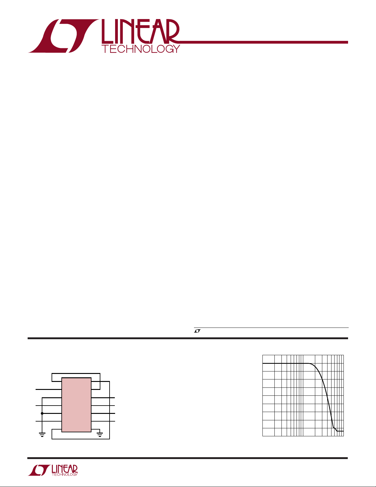
TYPICAL APPLICATIO
Butterworth 20kHz Anti-Aliasing Filter
1
V
IN
8V
NC
2
3
4
5
6
7
LTC1164-5
14
13
12
11
10
9
8
U
–8V
CLK = 1MHz
+
TO V
V
OUT
1164-5 TA01
WIDEBAND NOISE = 110µV
THD IN PASSBAND < 0.02% AT VIN = 2V
NOTE: THE CONNECTION FROM PIN 7 TO PIN 14
SHOULD BE MADE UNDER THE PACKAGE.
FOR 50:1 OPERATION CONNECT PIN 1 TO PIN 13
AS SHOWN. FOR 100:1 OR 150:1 OPERATION PINS 1
AND 13 SHOULD FLOAT. THE POWER SUPPLIES
SHOULD BE BYPASSED BY A 0.1µF CAPACITOR AS
CLOSE TO THE PACKAGE AS POSSIBLE.
RMS
RMS
0
–10
–20
–30
–40
GAIN (dB)
–50
–60
–70
–80
1
Frequency Response
10 100
FREQUENCY (kHz)
LTC1164-5 TA02
1
LTC1164-5
WW
W
ABSOLUTE AXI U RATI GS
U
(Note 1)
Total Supply Voltage (V+ to V–) ............................. 16V
Input Voltage (Note 2) ......... (V++ 0.3V) to (V– – 0.3V)
Output Short Circuit Duration ......................... Indefinite
Power Dissipation............................................. 400mW
Burn-In Voltage ...................................................... 16V
UUW
PACKAGE/ORDER I FOR ATIO
50:1 MODE
V
GND
V
GND
LP6
CONNECT 1
J PACKAGE
14-LEAD CERDIP
IN
+
T
T
JMAX
JMAX
1
2
3
4
5
6
7
= 150°C,
= 110°C,
TOP VIEW
θJA = 65°C/W (J)
θJA = 65°C/W (N)
CONNECT 2
14
50:1 MODE
13
–
V
12
CLK
11
BUTT/BESS
10
V
9
OUT
NC
8
N PACKAGE
14-LEAD PDIP
ORDER PART
NUMBER
LTC1164-5CN
LTC1164-5CJ
LTC1164-5MJ
Operating Temperature Range
LTC1164-5C ...................................... – 40°C to 85°C
LTC1164-5M .................................... –55°C to 125°C
Storage Temperature Range ................ –65°C to 150°C
Lead Temperature (Soldering, 10 sec)................. 300°C
50:1 MODE
V
GND
GND
NC
LP6
CONNECT 1
1
2
IN
3
+
4
V
5
6
7
8
16-LEAD PLASTIC SW
T
= 110°C,
JMAX
TOP VIEW
S PACKAGE
θJA = 85°C/W
16
15
14
13
12
11
10
9
CONNECT 2
50:1 MODE
–
V
NC
CLK
BUTT/BESS
NC
V
OUT
ORDER PART
NUMBER
LTC1164-5CS
Consult factory for Industrial grade parts.
ELECTRICAL CHARACTERISTICS
VS = ±7.5V, RL = 10k, f
PARAMETER CONDITIONS MIN TYP MAX UNITS
Passband Gain 0.1Hz at 0.25f
Gain at 0.50f
Gain at 0.90f
Gain at 0.95f
Gain at f
CUTOFF
Gain at 1.44f
Gain at 2.0f
Gain with f
Gain with VS = 2.375V (Note 3) fIN = 400kHz, fIN = 2kHz, (f
Input Frequency Range (f
(Note 3) fIN = 2kHz, (f
CUTOFF
(Note 3) fIN = 3.6kHz, (f
CUTOFF
(Note 3) fIN = 3.8kHz, (f
CUTOFF
(Note 3) fIN = 4kHz, (f
(Note 3) fIN = 5.76kHz, (f
CUTOFF
(Note 3) fIN = 8kHz, (f
CUTOFF
= 20kHz (Note 3) fIN = 200Hz, (f
CLK
= 400kHz, TA = Operating Temperature Range, unless otherwise specified.
CLK
(Note 3) fIN = 1kHz, (f
CUTOFF
f
= 1kHz, (f
IN
f
= 4kHz, (f
IN
= 8kHz, (f
f
IN
= 400kHz, fIN = 4kHz, (f
f
IN
) = 100:1 0 – <f
CLK/fC
) = 50:1 0 – <f
(f
CLK/fC
) = 100:1 ● –0.5 –0.10 0.25 dB
CLK/fC
) = 50:1 ● –0.5 0.10 0.25 dB
CLK/fC
) = 100:1 ● –0.45 –0.20 0.17 dB
CLK/fC
) = 50:1 ● –0.35 –0.10 0.40 dB
CLK/fC
) = 100:1 ● –2.50 –1.90 –1.0 dB
CLK/fC
) = 100:1 –2.60 dB
CLK/fC
) = 100:1 ● –4.10 –3.40 –2.75 dB
CLK/fC
) = 50:1 ● –4.20 –3.80 –2.75 dB
CLK/fC
) = 100:1 ● –20.5 –19.0 –17.0 dB
CLK/fC
) = 100:1 ● –45.0 –43.0 –41.0 dB
CLK/fC
) = 100:1 ● –4.50 –3.40 –2.75 dB
CLK/fC
) = 100:1 –0.50 –0.10 0.35 dB
CLK/fC
) = 100:1 –4.20 –3.40 –2.00 dB
CLK/fC
LTC1164-5C
/2 kHz
CLK
CLK
kHz
2
LTC1164-5
ELECTRICAL CHARACTERISTICS
VS = ±7.5V, RL = 10k, f
PARAMETER CONDITIONS MIN TYP MAX UNITS
Maximum f
Clock Feedthrough Input at GND, f = f
Wideband Noise Input at GND, 1Hz ≥ f < f
Input Impedance 70 100 160 kΩ
Output DC Voltage Swing VS = ±2.375V ● ±1.25 ±1.50 V
Output DC Offset VS = ±5V, (f
Output DC Offset TempCo VS = ±5V, (f
Power Supply Current VS = ±2.375V, TA ≥ 25°C 2.5 4.0 mA
Power Supply Range ±2.375 ±8V
The ● denotes specifications which apply over the full operating
temperature range.
Note 1: Absolute Maximum Ratings are those values beyond which life of
the device may be impaired.
CLK
= 400kHz, TA = Operating Temperature Range, unless otherwise specified.
CLK
VS ≥ ±7.5V 1.5 MHz
= ±5.0V 1.0 MHz
V
S
= Single 5V (GND = 2V) 1.0 MHz
V
S
, Square Wave
CLK
±5V, (f
±5V, (f
±5V, (f
±5V, (f
V
= ±5.0V ● ±3.70 ±4.10 V
S
= ±7.5V ● ±5.40 ±5.90 V
V
S
= ±5.0V, TA ≥ 25°C 4.5 7.0 mA
V
S
= ±7.5V, TA ≥ 25°C 7.0 11.0 mA
V
S
) = 100:1 200 µV
CLK/fC
) = 50:1 100 µV
CLK/fC
) = 100:1 100 ±5% µV
CLK/fC
) = 50:1 115 ±5% µV
CLK/fC
CLK/fC
CLK/fC
CLK
) = 100:1 ±50 ±160 mV
) = 100:1 ±100 µV/°C
● 4.5 mA
● 8.0 mA
● 12.5 mA
Note 2: Connecting any pin to voltages greater than V
may cause latchup. It is recommended that no sources operating from
external supplies be applied prior to power-up of the LTC1164-5.
Note 3: All gains are measured relative to passband gain. The filter cutoff
frequency is abbreviated as f
CUTOFF
LTC1164-5C
or fC.
+
or less than V
RMS
RMS
RMS
RMS
–
UW
TYPICAL PERFOR A CE CHARACTERISTICS
Gain vs Frequency
A. f
= 100kHz
CLK
f
0
–10
–20
–30
–40
GAIN (dB)
–50
–60
–70
–80
0.1
VS = ±5V
= 25°C
T
A
ACB
110
FREQUENCY (kHz)
LTC1164-5 • G01
50
= 1kHz
CUTOFF
(100:1, PIN 10 TO V–)
= 375kHz
B. f
CLK
f
= 2.68kHz
CUTOFF
(140:1, PIN 10 GND)
= 500kHz
C. f
CLK
= 10kHz
f
CUTOFF
(50:1, PIN 10 TO V+,
PINS 1-13 SHORTED)
Passband Gain and Phase
vs Frequency
0
–5
GAIN (dB)
–10
VS = ±5V
= 50kHz
f
CLK
= 1kHz
f
CUTOFF
–15
(50:1, PIN 10 TO V
PINS 1-13 SHORTED)
= 25°C
T
A
0.2
+
0.4
FREQUENCY (kHz)
0
GAIN
PHASE
,
0.8
0.6
1.0
LTC1164-5 • G02
–90
–180
–270
PHASE (DEG)
3
LTC1164-5
FREQUENCY (kHz)
0.1
–4.0
GAIN (dB)
–3.5
–2.5
–2.0
–1.5
–0.5
1
10
LTC1164-5 • G06
–3.0
0
0.5
–1.0
AEFB C D
A. f
CLK
= 200kHz
f
CUTOFF
= 4kHz
B. f
CLK
= 300kHz
f
CUTOFF
= 6kHz
C. f
CLK
= 500kHz
f
CUTOFF
= 10kHz
D. f
CLK
= 750kHz
f
CUTOFF
= 15kHz
E. f
CLK
= 1MHz
f
CUTOFF
= 20kHz
F. f
CLK
= 1.5MHz
f
CUTOFF
= 30kHz
VS = ±7.5V
50:1
T
A
= 25°C
30
UW
TYPICAL PERFOR A CE CHARACTERISTICS
Passband Gain and Phase
vs Frequency
0
–5
GAIN (dB)
–10
VS = ±5V
f
= 100kHz
CLK
–15
–20
= 1kHz
f
CUTOFF
(100:1, PIN 10 TO V
= 25°C
T
A
0.4
0.2
FREQUENCY (kHz)
Group Delay vs Frequency
500
VS = ±7.5V
450
= 25°C
T
A
400
350
300
250
200
A
GROUP DELAY (µs)
150
100
B
50
0
0.5
1.5
3.5
2.5
FREQUENCY (kHz)
–
0.6
Passband Gain and Phase
vs Frequency
0
PHASE (DEG)
–90
–180
–270
)
4.5
0.8
LTC1164-5 • G03
5.5
LTC1164-5 • G05
6.5
1.0
–360
= 500kHz
A. f
CLK
(BUTTERWORTH 100:1)
f
CUTOFF
= 750kHz
B. f
CLK
(BESSEL 140:1)
f
CUTOFF
7.5
= 5kHz
= 5.36kHz
0
–5
GAIN (dB)
–10
VS = ±5V
= 150kHz
f
CLK
–15
–20
= 1.07kHz
f
CUTOFF
(140:1, PIN 10 TO GND)
= 25°C
T
A
0.4
0.2
0.6
FREQUENCY (kHz)
Passband vs Frequency and f
GAIN
PHASE
0.8
1.0
LTC1164-5 • G04
CLK
0
PHASE (DEG)
–90
–180
–270
–360
4
Maximum Passband over
Temperature for VS = ±7.5V, 50:1 Passband vs Frequency and f
0.5
0
–0.5
–1.0
–1.5
GAIN (dB)
–2.0
–2.5
–3.0
VS = ±7.5V
= 1.5MHz (50:1)
f
CLK
–3.5
f
CUTOFF
–4.0
1
= 30kHz
FREQUENCY (kHz)
TA = 70°C
TA = –40°C
10
LTC1164-5 • G07
30
0.5
0
–0.5
–1.0
–1.5
GAIN (dB)
–2.0
–2.5
–3.0
–3.5
–4.0
0.1
VS = ±7.5V
100:1
= 25°C
T
A
A
1
FREQUENCY (kHz)
B C D
LTC1164-5 • G08
CLK
10
A. f
= 200kHz
CLK
= 2kHz
f
CUTOFF
= 500kHz
B. f
CLK
= 5kHz
f
CUTOFF
E
= 750kHz
C. f
CLK
= 7.5kHz
f
CUTOFF
= 1MHz
D. f
CLK
= 10kHz
f
CUTOFF
= 1.5MHz
E. f
CLK
= 15kHz
f
CUTOFF
20
 Loading...