

Linear Technology LTC1159IS-5, LTC1159IS-3.3, LTC1159IS, LTC1159CS-5, LTC1159CS-3.3 Datasheet
...
FEATURES
■
Operation from 4V to 40V Input Voltage
■
Ultrahigh Efficiency: Up to 95%
■
20µA Supply Current in Shutdown
■
High Efficiency Maintained Over Wide Current Range
■
Current Mode Operation for Excellent Line and Load
Transient Response
■
Very Low Dropout Operation: 100% Duty Cycle
■
Short-Circuit Protection
■
Synchronous FET Switching for High Efficiency
■
Adaptive Non-Overlap Gate Drives
■
Available in SSOP and SO Packages
U
APPLICATIO S
■
Step-Down and Inverting Regulators
■
Notebook and Palmtop Computers
■
Portable Instruments
■
Battery-Operated Digital Devices
■
Industrial Power Distribution
■
Avionics Systems
■
Telecom Power Supplies
LTC1159
LTC1159-3.3/LTC1159- 5
High Efficiency Synchronous
Step-Down Switching Regulators
U
DESCRIPTIO
The LTC®1159 series is a family of synchronous step-down
switching regulator controllers featuring automatic Burst
ModeTM operation to maintain high efficiencies at low
output currents. These devices drive external complementary power MOSFETs at switching frequencies up to 250kHz
using a constant off-time current-mode architecture.
A separate pin and on-board switch allow the MOSFET
driver power to be derived from the regulated output
voltage providing significant efficiency improvement when
operating at high input voltages. The constant off-time
current-mode architecture maintains constant ripple current in the inductor and provides excellent line and load
transient response. The output current level is user programmable via an external current sense resistor.
The LTC1159 automatically switches to power saving
Burst Mode operation when load current drops below
approximately 15% of maximum current. Standby current
is only 300µA while still regulating the output and shut-
down current is a low 20µA.
, LTC and LT are registered trademarks of Linear Technology Corporation.
Burst Mode is a trademark of Linear Technology Corporation.
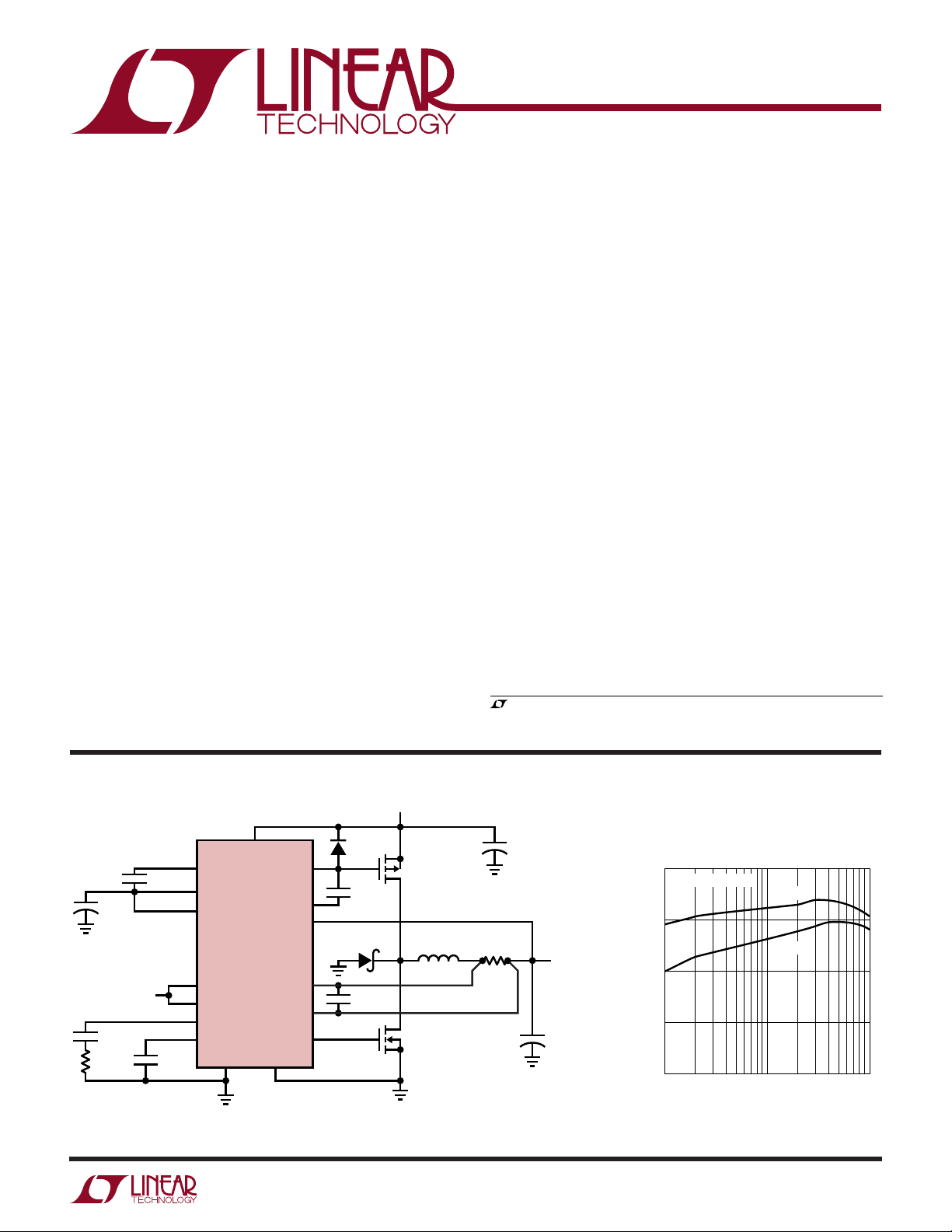
TYPICAL APPLICATIO
V
IN
+
3.3µF
0V = NORMAL
>2V = SHUTDOWN
3300pF
1k
C
T
300pF
CAP
V
CC
V
CC
SHDN1
SHDN2
I
TH
C
T
S-GND
0.15µF
Figure 1. High Efficiency Step-Down Regulator
P-GATE
P-DRIVE
EXTV
LTC1159-5
SENSE
SENSE
N-GATE
P-GND
U
V
IN
+
C
R
SENSE
0.05Ω
IN
100µF
100V
21
4
+
V
OUT
5V/2A
C
OUT
220µF
100
FIGURE 1 CIRCUIT
90
80
EFFICIENCY (%)
70
60
0.02
LTC1159-5 Efficiency
VIN = 10V
VIN = 20V
0.2 2
LOAD CURRENT (A)
LTC1159 • TA01
1N4148
Si9435DY
0.1µF
CC
+
–
D1
MBRS140T3
0.01µF
LTC1159 • F01
L*
33µH
3
Si9410DY
*COILTRONICS CTX33-4-MP
1
LTC1159
LTC1159-3.3/LTC1159-5
A
W
O
LUTEXI TIS
S
A
WUW
U
ARB
G
(Note 1)
Input Supply Voltage (Pin 2) ..................... –15V to 60V
VCC Output Current (Pin 3) .................................. 50mA
Continuous Pin Currents (Any Pin)...................... 50mA
Sense Voltages ......................................... –0.3V to 13V
Shutdown Voltages................................................... 7V
EXTVCC Input Voltage ............................................. 15V
Junction Temperature (Note 2)............................ 125°C
WU
/
PACKAGE
P-GATE
V
IN
V
CC
P-DRIVE
P-DRIVE
V
CC
V
CC
C
T
I
TH
–
SENSE
T
O
RDER I FOR ATIO
TOP VIEW
1
2
3
4
5
6
7
8
9
10
G PACKAGE
20-LEAD PLASTIC SSOP
JMAX
= 125°C, θ
= 135°C/W
JA
20
19
18
17
16
15
14
13
12
11
CAP
SHDN2
EXTV
PGND
N-GATE
PGND
SGND
SHDN1
V
FB
SENSE
ORDER PART
NUMBER
CC
LTC1159CG
LTC1159CG-3.3
LTC1159CG-5
+
Operating Temperature Range
LTC1159C .............................................. 0°C to 70°C
LTC1159I........................................... –40°C to 85°C
Extended Commercial
Temperature Range ............................... – 40°C to 85°C
Storage Temperature Range ................ –65°C to 150°C
Lead Temperature (Soldering, 10 sec)................. 300°C
U
ORDER PART
NUMBER
LTC1159CN
LTC1159CN-3.3
LTC1159CN-5
LTC1159CS
LTC1159CS-3.3
LTC1159CS-5
LTC1159IS
LTC1159IS-3.3
LTC1159IS-5
1
P-GATE
2
V
IN
3
V
CC
P-DRIVE
SENSE
4
5
V
CC
6
C
T
7
I
TH
–
8
N PACKAGE
16-LEAD PDIP
*FIXED OUTPUT VERSIONS
T
= 125°C, θ
JMAX
T
= 125°C, θ
JMAX
TOP VIEW
S PACKAGE
16-LEAD PLASTIC SO
= 80°C/ W (N)
JA
= 110°C/ W (S)
JA
16
15
14
13
12
11
10
9
CAP
SHDN2
EXTV
N-GATE
PGND
SGND
V
(SHDN1)*
FB
SENSE
CC
+
Consult LTC Marketing for parts specified with wider operating temperature ranges.
LECTRICAL C CHARA TERIST
E
ICS
temperature range, otherwise specifications are at TA = 25°C. VIN = 12V, V
SYMBOL PARAMETER CONDITIONS MIN TYP MAX UNITS
V
FB
I
FB
V
OUT
∆V
OUT
I
IN
I
EXTVCC
Feedback Voltage (LTC1159 Only) ● 1.21 1.25 1.29 V
Feedback Current (LTC1159 Only) ● 0.2 µA
Regulated Output Voltage VIN = 9V
LTC1159-3.3 I
LTC1159-5 I
Output Voltage Line Regulation VIN = 9V to 40V –40 0 40 mV
Output Voltage Load Regulation
LTC1159-3.3 5mA < I
LTC1159-5 5mA < I
Burst Mode Output Ripple I
VIN Pin Current (Note 4)
Normal Mode V
Shutdown VIN = 12V, V
EXTVCC Pin Current (Note 4) EXTVCC = 5V, Sleep Mode 250 µA
LOAD
LOAD
LOAD
IN
V
IN
V
IN
The ● denotes specifications which apply over the full operating
= 0V (Note 3), unless otherwise noted.
SHDN1
= 700mA ● 3.23 3.33 3.43 V
= 700mA ● 4.90 5.05 5.20 V
< 2A ● 40 65 mV
LOAD
< 2A ● 60 100 mV
LOAD
= 0A 50 mV
= 12V, EXTVCC = 5V 200 µA
= 40V, EXTVCC = 5V 300 µA
= 2V 15 µA
= 40V, V
SHDN2
= 2V 25 µA
SHDN2
P-P
2
LTC1159
LTC1159-3.3/LTC1159- 5
LECTRICAL C CHARA TERIST
E
ICS
temperature range, otherwise specifications are at TA = 25°C. VIN = 12V, V
The ● denotes specifications which apply over the full operating
= 0V (Note 3), unless otherwise noted.
SHDN1
SYMBOL PARAMETER CONDITIONS MIN TYP MAX UNITS
V
CC
VIN – V
V
– V
EXT
V
P-GATE
Internal Regulator Voltage VIN = 12V to 40V, EXTVCC = 0V, ICC = 10mA ● 4.25 4.5 4.75 V
VCC Dropout Voltage VIN = 4V, EXTVCC = Open, ICC = 10mA 300 400 mV
CC
EXTVCC Switch Drop VIN = 12V, EXTVCC = 5V, I
CC
= 10mA 250 350 mV
SWITCH
– VINP-Gate to Source Voltage (Off) VIN = 12V –0.2 0 V
VIN = 40V –0.2 0 V
+
V
– Current Sense Threshold Voltage
SENSE
V
SENSE
V
SNDN1
–
LTC1159 V
LTC1159-3.3 V
LTC1159-5 V
SHDN1 Threshold
–
= 5V, VFB = 1.32V (Forced) 25 mV
SENSE
–
V
= 5V, VFB = 1.15V (Forced) ● 130 150 170 mV
SENSE
–
= 3.4V (Forced) 25 mV
SENSE
–
= 3.1V (Forced) ● 130 150 170 mV
V
SENSE
–
= 5.2V (Forced) 25 mV
SENSE
–
= 4.7V (Forced) ● 130 150 170 mV
V
SENSE
LTC1159CG, LTC1159-3.3, LTC1159-5 0.5 0.8 2 V
V
SHDN2
I
SHDN2
I
CT
t
OFF
tr, t
f
SHDN2 Threshold 0.8 1.4 2 V
Shutdown 2 Input Current V
CT Pin Discharge Current V
Off-Time (Note 5) CT = 390pF, I
= 5V 12 20 µA
SHDN2
in Regulation 50 70 90 µA
OUT
= 0V 2 10 µA
V
OUT
= 700mA, VIN = 10V 4 5 6 µs
LOAD
Driver Output Transition Times CL = 3000pF (Pins P-Drive and N-Gate), VIN = 6V 100 200 ns
–40°C ≤ TA ≤ 85°C (Note 6)
SYMBOL PARAMETER CONDITIONS MIN TYP MAX UNITS
V
FB
V
OUT
I
IN
I
EXTVCC
V
CC
+
V
SENSE
–
V
SENSE
V
SHDN2
t
OFF
Note 1: Absolute Maximum Ratings are those values beyond which the life
of a device may be impaired.
Note 2: T
dissipation P
LTC1159CG, LTC1159CG-3.3, LTC1159CG-5: T
LTC1159CN, LTC1159CN-3.3, LTC1159CN-5: T
LTC1159CS, LTC1159CS-3.3, LTC1159CS-5: T
Feedback Voltage (LTC1159 Only) 1.2 1.25 1.3 V
Regulated Output Voltage VIN = 9V
LTC1159-3.3 I
LTC1159-5 I
= 700mA 3.17 3.30 3.43 V
LOAD
= 700mA 4.85 5.05 5.25 V
LOAD
VIN Pin Current (Note 4)
Normal V
= 12V, EXTVCC = 5V 200 µA
IN
VIN = 40V, EXTVCC = 5V 300 µA
Shutdown VIN = 12V, V
VIN = 40V, V
= 2V 15 µA
SHDN2
= 2V 25 µA
SHDN2
EXTVCC Pin Current (Note 4) EXTVCC = 5V, Sleep Mode 250 µA
Internal Regulator Voltage VIN = 12V to 40V, EXTVCC = 0V, ICC = 10mA 4.5 V
– Current Sense Threshold Voltage Low Threshold (Forced) 25 mV
High Threshold (Forced) 125 150 175 mV
SHDN2 Threshold 0.8 1.4 2 V
Off-Time (Note 5) CT = 390pF, I
= 700mA, VIN = 10V 3.5 5 6.5 µs
LOAD
Note 3: On LTC1159 versions which have a SHDN1 pin, it must be at
ground potential for testing.
is calculated from the ambient temperature TA and power
J
according to the following formulas:
D
= TA + (PD • 135°C/W)
J
= TA + (PD • 80°C/W)
J
= TA + (PD • 110°C/W)
J
Note 4: The LTC1159 V
MOSFET driver currents. When V
, the input current increases by (I
EXTV
CC
and EXTVCC current measurements exclude
IN
power is derived from the output via
CC
• Duty Cycle)/(Efficiency).
GATECHG
See Typical Performance Characteristics and Applications Information.
Note 5: In applications where R
is placed at ground potential, the off-
SENSE
time increases approximately 40%.
3
LTC1159
LOAD CURRENT (A)
0
–100
∆V
OUT
(mV)
–80
–60
–40
–20
0
20
0.5 1.0 1.5 2.0
LTC1159 • TPC03
2.5
FIGURE 1 CIRCUIT
V
IN
= 24V
LTC1159-3.3/LTC1159-5
LECTRICAL C CHARA TERIST
E
ICS
Note 6: The LTC1159C, LTC1159C-3.3, and LTC1159C-5 are not tested
and not quality assurance sampled at –40°C and 85°C. These
specifications are guaranteed by design and/or correlation. The LTC1159I,
LTC1159I-3.3 and LTC1159I-5 are guaranteed and tested over the –40°C
Note 7: The logic-level power MOSFETs shown in Figure 1 are rated for
V
= 30V. For operation at VIN > 30V, use standard threshold
DS(MAX)
MOSFETs with EXTV
Information.
to 85°C operating temperature range.
UW
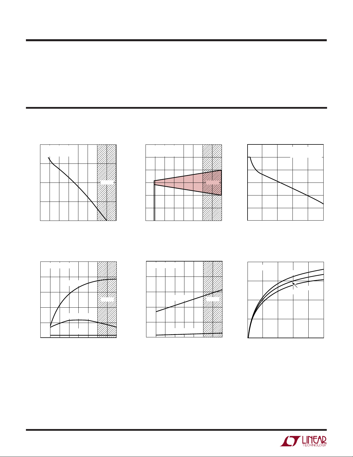
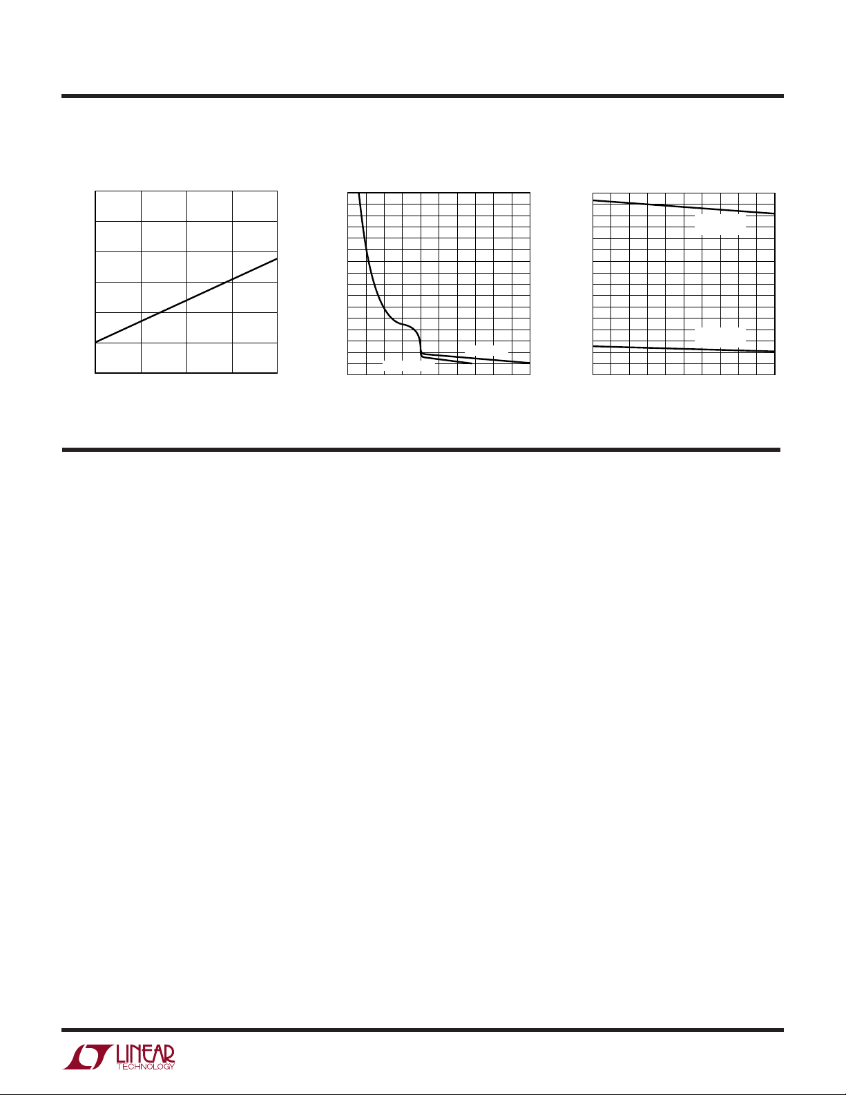
TYPICAL PERFOR A CE CHARACTERISTICS
Efficiency vs Input Voltage
100
FIGURE 1 CIRCUIT
I
= 1A
LOAD
95
90
EFFICIENCY (%)
85
80
0
5101520
INPUT VOLTAGE (V)
NOTE 6
25 30 35 40
LTC1159 • TPC01
Line Regulation
60
FIGURE 1 CIRCUIT
= 1A
I
LOAD
40
20
(mV)
0
OUT
∆V
–20
–40
–60
0
515
10 20
INPUT VOLTAGE (V)
30
25
NOTE 6
35
LT1159 • TPC02
powered from a 12V supply. See Applications
CC
Load Regulation
40
Operating Frequency
EXTVCC Pin Current
10
FIGURE 1 CIRCUIT
8
I
= 1A
LOAD
6
CURRENT (mA)
4
CC
I
= 100mA
EXTV
2
0
0
510
LOAD
I
= 0
LOAD
20
15 25 40
INPUT VOLTAGE (V)
NOTE 6
30 35
LTC1159 • TPC04
VIN Pin Current
500
FIGURE 1 CIRCUIT
400
300
200
SUPPLY CURRENT (µA)
100
0
0
510
INPUT VOLTAGE (V)
NORMAL
V
= 2V
SHDN2
20
15 25 40
NOTE 6
30 35
LTC1159 • TPC05
vs (VIN – V
2.0
V
= 5V
OUT
1.5
1.0
0.5
NORMALIZED FREQUENCY
0
0
5
(VIN – V
OUT
10
OUT
)
T = 0°C
T = 70°C
15
) VOLTAGE (V)
T = 25°C
20
25
LTC1159 • TPC06
4
UW
TYPICAL PERFOR A CE CHARACTERISTICS
LTC1159
LTC1159-3.3/LTC1159- 5
EXTVCC Switch Drop Current Sense Threshold Voltage
600
500
400
(mV)
CC
300
– V
CC
200
EXTV
100
0
0
5101520
SWITCH CURRENT (mA)
LTC1159 • TPC07
U
UU
Off-Time vs V
80
70
60
50
40
30
OFF-TIME (µs)
20
10
0
0
OUT
LTC1159-3.3
1
2
OUTPUT VOLTAGE (V)
LTC1159-5
34
LTC1159 • TPC08
5
160
140
120
100
80
60
SENSE VOLTAGE (mV)
40
20
0
0
20
MAXIMUM
THRESHOLD
THRESHOLD
60 80
40
TEMPERATURE (°C)
PI FU CTIO S
VIN: Main Supply Input Pin.
SGND: Small-Signal Ground. Must be routed separately
from other grounds to the (–) terminal of C
OUT
.
PGND: Driver Power Grounds. Connect to source of Nchannel MOSFET and the (–) terminal of CIN.
VCC: Outputs of internal 4.5V linear regulator, EXTV
switch, and supply inputs for driver and control circuits.
The driver and control circuits are powered from the higher
of the 4.5V regulator or EXTVCC voltage. Must be closely
decoupled to power ground.
SENSE+: The (+) Input for the Current Comparator. A builtin offset between the SENSE+ and SENSE– pins, in conjunction with R
, sets the current trip threshold.
SENSE
N-Gate: High Current Drive for the Bottom N-Channel
MOSFET. The N-Gate pin swings from ground to VCC.
P-Gate: Level-Shifted Gate Drive Signal for the Top
CC
P-Channel MOSFET. The voltage swing at the P-gate pin is
from VIN to VIN – VCC.
P-Drive: High Current Gate Drive for the Top P-Channel
MOSFET. The P-drive pin(s) swing(s) from VCC to ground.
MINIMUM
100
LTC1159 • TPC09
CT: External capacitor CT from this pin to ground sets the
operating frequency. (The frequency is also dependent on
the ratio V
OUT/VIN
.)
ITH: Gain Amplifier Decoupling Point. The current comparator threshold increases with the I
pin voltage.
TH
VFB: For the LTC1159 adjustable version, the VFB pin
receives the feedback voltage from an external resistive
divider used to set the output voltage.
SENSE–: Connects to internal resistive divider which sets
the output voltage in fixed output versions. The SENSE– pin
is also the (–) input of the current comparator.
CAP: Charge Compensation Pin. A capacitor to VCC pro-
vides charge required by the P-gate level-shift capacitor
during supply transitions.
pacitor must be larger than the gate drive capacitor
SHDN1: This pin shuts down the control circuitry only (V
The charge compensation ca-
.
CC
is not affected). Taking SHDN1 pin high turns off the
control circuitry and holds both MOSFETs off. This pin
must be at ground potential for normal operation.
SHDN2: Master Shutdown Pin. Taking SHDN2 high shuts
down VCC and all control circuitry.
5
LTC1159
LTC1159-3.3/LTC1159-5
U
U
W
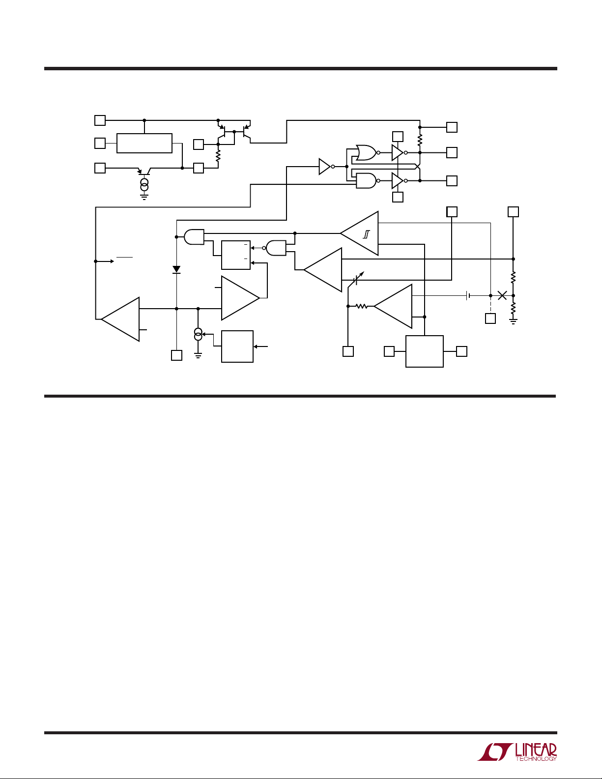
FU CTIO AL DIAGRA
V
IN
SHDN2
EXTV
LOW DROPOUT
4.5V REGULATOR
CC
LOW DROP SWITCH
SLEEP
+
S
V
–
TH2
CAP
V
CC
V
C
T
Internal divider broken at VFB for adjustable versions.
550k
PGND
–
V
+
25mV TO 150mV
13k
SGND
TH
TH1
Q
–
T
+
OFF-TIME
CONTROL
R
S
–
SENSE
–
C
+
I
V
CC
G
550k
–
+
1.25V
REFERENCE
SENSE
P-GATE
P-DRIVE
N-GATE
+
V
OS
SHDN1
–
SENSE
100k
LTC1159 • FD
V
FB
U
OPERATIO
The LTC1159 uses a current mode, constant off-time
architecture to synchronously switch an external pair of
complementary power MOSFETs. Operating frequency is
set by an external capacitor at the CT pin.
The output voltage is sensed either by an internal voltage
divider connected to the SENSE– pin (LTC1159-3.3 and
LTC1159-5) or an external divider returned to the VFB pin
(LTC1159). A voltage comparator V, and a gain block G,
compare the divided output voltage with a reference voltage of 1.25V. To optimize efficiency, the LTC1159 automatically switches between two modes of operation, burst
and continuous.
A low dropout 4.5V regulator provides the operating voltage VCC for the MOSFET drivers and control circuitry during
start-up. During normal operation, the LTC1159 family
powers the drivers and control from the output via the
EXTVCC pin to improve efficiency. The N-GATE pin is
referenced to ground and drives the N-channel MOSFET
gate directly. The P-channel gate drive must be referenced
to the main supply input VIN, which is accomplished by
(Refer to Functional Diagram)
level-shifting the P-drive signal via an internal 550k resistor
and external capacitor.
During the switch “ON” cycle in continuous mode, current
comparator C monitors the voltage between the SENSE
+
and SENSE– pins connected across an external shunt in
series with the inductor. When the voltage across the shunt
reaches its threshold value, the P-gate output is switched
to VIN, turning off the P-channel MOSFET. The timing
capacitor CT is now allowed to discharge at a rate determined by the off-time controller. The discharge current is
made proportional to the output voltage to model the
inductor current, which decays at a rate which is also
proportional to the output voltage. While the timing
capacitor is discharging, the N-gate output is high, turning
on the N-channel MOSFET.
When the voltage on CT has discharged past V
, compara-
TH1
tor T trips, setting the flip-flop. This causes the N-gate output
to go low (turning off the N-channel MOSFET) and the Pgate output to also go low (turning the P-channel MOSFET
back on). The cycle then repeats. As the load current
6
 Loading...