

Page 1

Embedded &
Industrial Computing
Hardware Platforms for Embedded and Industrial Computing
LEC-2136
V1.1
>>
User's Manual
Publication date:2014-03-11
Page 2

About
About
Overview
Icon Descriptions
The icons are used in the manual to serve as an indication
of interest topics or important messages. Below is a
description of these icons:
NOTE: This check mark indicates that
there is a note of interest and is something
that you should pay special attention to
while using the product.
Online Resources
The listed websites are links to the on-line product
information and technical support.
Resource Website
Lanner http://www.lannerinc.com
Product Resources
RMA http://eRMA.lannerinc.com
WARNING: This exclamation point
indicates that there is a caution or
warning and it is something that could
damage your property or product.
http://www.lannerinc.com/
download-center/
Acknowledgement
Intel, Pentium and Celeron are registered trademarks of
Intel Corp.
Microsoft Windows and MS-DOS are registered trademarks
of Microsoft Corp.
All other product names or trademarks are properties of
their respective owners.
Compliances and Certification
CE Certication
This product has passed the CE test for environmental
specifications. Test conditions for passing included the
equipment being operated within an industrial enclosure.
In order to protect the product from being damaged by
ESD (Electrostatic Discharge) and EMI leakage, we strongly
recommend the use of CE-compliant industrial enclosure
products.
FCC Class A Certication
This equipment has been tested and found to comply
with the limits for a Class A digital device, pursuant to Part
15 of the FCC Rules. These limits are designed to provide
reasonable protection against harmful interference when
the equipment is operated in a commercial environment.
This equipment generates, uses and can radiate radio
frequency energy and, if not installed and used in
accordance with the instruction manual, may cause
harmful interference to radio communications. Operation
of this equipment in a residential area is likely to cause
harmful interference in which case the user will be required
to correct the interference at his own expense.
Revision History
Copyright and Trademarks
This document is copyrighted, © 2014 All rights are
reserved. The original manufacturer reserves the right to
make improvements to the products described in this
manual at any time without notice.
No part of this manual may be reproduced, copied,
translated or transmitted in any form or by any means
without the prior written permission of the original
manufacturer. Information provided in this manual is
intended to be accurate and reliable. However, the original
manufacturer assumes no responsibility for its use, nor for
any infringements upon the rights of third parties that
may result from such use.
Embedded and Industrial Computing
Version Changes
1.1 Change the super I/O chip to
W83627DHG-P
2
Page 3

TTaTTable of Contentsbeable of Contents
Chapter 1: Introduction 4
System Specication . . . . . . . . . . . . . . . . . . . . . . . . . . . . . . . . . . . . . . . . . . . 4
Package Contents . . . . . . . . . . . . . . . . . . . . . . . . . . . . . . . . . . . . . . . . . . . . . 5
Chapter 2: System Components 6
System Drawing . . . . . . . . . . . . . . . . . . . . . . . . . . . . . . . . . . . . . . . . . . . . . . 6
Block Diagram . . . . . . . . . . . . . . . . . . . . . . . . . . . . . . . . . . . . . . . . . . . . . . . 7
Front Components. . . . . . . . . . . . . . . . . . . . . . . . . . . . . . . . . . . . . . . . . . . . . 8
Rear Components . . . . . . . . . . . . . . . . . . . . . . . . . . . . . . . . . . . . . . . . . . . . . 9
Chapter 3: Board Layout 10
External Connectors. . . . . . . . . . . . . . . . . . . . . . . . . . . . . . . . . . . . . . . . . . . .10
Internal Connectors and Jumpers . . . . . . . . . . . . . . . . . . . . . . . . . . . . . . . . . . .11
Connectors and Jumpers List. . . . . . . . . . . . . . . . . . . . . . . . . . . . . . . . . . . . . .12
Jumper Settings . . . . . . . . . . . . . . . . . . . . . . . . . . . . . . . . . . . . . . . . . . . . . .13
Chapter 4: Hardware Setup 16
Preparing the Hardware Installation. . . . . . . . . . . . . . . . . . . . . . . . . . . . . . . . . .16
System Memory Installation. . . . . . . . . . . . . . . . . . . . . . . . . . . . . . . . . . . . . . .16
Hard Disk Installation . . . . . . . . . . . . . . . . . . . . . . . . . . . . . . . . . . . . . . . . . . .16
CompactFlash Card Installation. . . . . . . . . . . . . . . . . . . . . . . . . . . . . . . . . . . . .17
3G SIM Card Installation . . . . . . . . . . . . . . . . . . . . . . . . . . . . . . . . . . . . . . . . .17
3G Wireless Module Installation . . . . . . . . . . . . . . . . . . . . . . . . . . . . . . . . . . . .17
Wall Mounting . . . . . . . . . . . . . . . . . . . . . . . . . . . . . . . . . . . . . . . . . . . . . . .18
Appendix A: Programming Watchdog Timer 19
3
Page 4

Chapter 1
Introduction
Chapter 1:
Introduction
Thank you for choosing the LEC-2136. This product has
an embedded ultra-low voltage Intel Pineview Processor
ATOM D525 (Dual Core,1M cache,1.8GHz) CPU, which
delivers power-efficient processing. This fanless and
compact platform can be broadly applied across industries
from networking, portable medical, industrial control
while maintaining low power consumption with good
performance.
Here is the list of key features:
Intel integrated Graphics Media Accelerator 3150 •
which supports VGA (up to 2048x1536)
One RJ-45 Management Port 10/100/1000 Mbps LAN •
(provided by 82574L)
5 10/100/1000 Mbps LAN (provided by Intel 82583V) •
One • Mini-PCIe expansion slots (paired with a SIM card
reader to support 3G Internet service)
One SATA hard disk and one CompactFlash support •
One RS-232 serial port via DB9 and one RS-232 serial •
port via pin headers
4 USB Type A connector •
System Specification
LEC 2 Series
Dimension (WxHxD)
Processor
Chipset
System
Memory
Storage
Ethernet Controller
Graphic Controller
IO
Power Input
Hardware Monitor
OS Support
Certications
Compliance
Operating Temperature Range
with
Commercial Components
Technology DDR3 667/800 MHz, non-ECC
Max. Capacity Up to 4GB
IDE CF socket Type I/II x1
SATA 2.5” HDD/SSD drive bay x1
VGA
LAN GbE RJ45 x6
Display
Video Grabber No
Serial I/O DB9 x1 for RS232;
USB 2.0 Type A x4
Power Input DC_in with Phoenix contact
Expansion
Others
LEC-2136
198x42x144.8mm
(7.722”x1.638”x5.6472”)
Intel Atom D525 1.8GHz
Intel ICH8M
1 x Intel 82574L LAN Chip
5 x Intel 82583V LAN Chip
Intel GMA3150
DB15 x1 for VGA, DVI-D
(sup to 2048x1536)
Mini-PCIe x1 (with SIM card
reader)
External: Power-on button,
Power-on switch, 3x SMA
antenna hole, reset.
Internal: PS/2 keyboard and
mouse
+24Vdc 2.5A
Winbond W83627DHG-P
integrated watchdog timer
1~255 level
Linux , XPE/WES2009, XP PRO
FES, WS7E, WS7P, WIN 7 PRO-E
CE, FCC Class A
No
-5~45°C/23~113°F
Embedded and Industrial Computing
4
Page 5

Chapter 1
Package Contents
Your package contains the following items:
LEC-2136 Embedded System •
DC+12V 60W Power Adapter (24V 60W •
0P0W060240A01)
Serial-ATA/Power Cable (P/N: 080W1N2201001) •
Wall-Mounting Kit (P/N: SE • 9ESA900R100)
Drivers and User’s Manual CD •
Introduction
Embedded and Industrial Computing
5
Page 6
Chapter 2
Chapter 2:
System Components
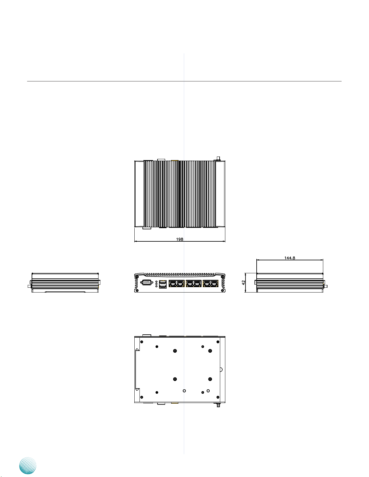
System Drawing
Mechanical dimensions of the LEC-2136
Unit: mm
System Components
Embedded and Industrial Computing
6
Page 7

Chapter 2
Intel
ICH8M
Processor
ATOM D525
Winbond
W83627UHG
H/W Monitor
WDT
PS/2 KB/MS
Pin Header
SATA
VGA
GbE LAN
1x82574L
5x82583V
2x PCIe
IDE
DDR3
1xSO-DIMM
Mini PCI Express
Socket
USB
SIM Card Reader
Serial Port
RS232
1x DB-9
6x RJ-45
SATA-II
2x Connector
Compact Flash
Socket
LPC
BIOS Flash
SPI
VGA
4xDMI
USB
USB 2.0 Ports
4x Type A
Block Diagram
The block diagram depicts the relationships among the
interfaces and modules on the motherboard..
System Components
Embedded and Industrial Computing
W83627DHG-P
7
Page 8

Chapter 2
Front Components
System Components
F1
Component Description Pin Definition Reference
F1 Power Button with dual LED ATX Power-on button with LEDs:
Standby mode in Red; Power-on mode
in Green
F2 Dual USB 2.0 Stack Connector An USB type A connector. Besides this
one, there is another Dual USB connectors on the back panel.
F3 VGA Port The VGA port is provided by integrat-
ed Graphics Media Accelerator 3150.
The displays can support VGA up to
2048x1536.
F4 DC-In (power) Power-in Connector through 1x2 Pin
Phoenix Contact Connector. The input
power should be 24V 2.5A.
F5 Reset Reset switch
The reset switch can be programmed
to be either a software or hardware
reset. The software reset can set the
designated software to its default
settings. The hardware reset will
trigger the reset signal and reboot the
whole system. Refer to JP2 jumper
in Chapter 3 Board Layout and the
sample code on the Driver and User
Manual CD.
F2 F3
F4
F5
CN2 on page 14
CN10 on page14
VGA1 on page 13
CN9 on page 14
SW1 on page 13
Embedded and Industrial Computing
8
Page 9

Chapter 2
System Components
Rear Components
R1 R2 R3 R4
Component Description Pin Definition Reference
R1 Serial Port COM1 Serial ports through the DB-9
connector; COM1 supports RS232 protocol. The system also has
another COM port (COM2) via the
internal pin header.
R2 HDD (Yellow), Status and
Power LED (Green)
R3 Dual USB2.0 Stack
Connector
R4 Dual 10/100/1000 LAN
Ports
LINK/ACT
SPEED
Embedded and Industrial Computing
HDD
Blinking: data access activities•
Off: no data access activities•
Status. This LED can be programmed
to behave like this (refer to the Driver
and User Manual CD for sample code):
Red: abnormal condition arises•
Off: normal operation•
Power
On: The computer is on.•
Off: The computer is off .•
An USB type A connector.Besides
this one, there is another Dual USB
connectors on the front panel.
Two RJ-45 (network) jacks with LED
indicators as described below. The
LAN ports are provided by Intel
82574L and 82583V. The LAN1
(powered by 82574L) can serve
management functions including
the PXE (Preboot eXecution
Environment; you need to turn on the
PXE in the BIOS).
LINK/ACT (Yellow)
On/Flashing: The port is linking •
and active in data transmission.
Off: The port is not linking.•
SPEED (Green/Amber)
Amber: The connection speed is •
1000Mbps.
Green: The connection speed is •
100Mbps
Off: .The connection speed is •
10Mbps.
COM1on page 13
CN7 on Page 14
LAN1/LAN2/LAN3 on page 14
9
Page 10

Chapter 3
Chapter 3:
Board Layout
External Connectors
The following picture highlights the location of system
input/output connectors. Refer to the table 3.1 Connector
List for more details.
Board Layout
CN2
CN10
VGA1
DC_IN
LAN3
Embedded and Industrial Computing
LAN2
LAN1
CN7
COM1
10
Page 11

Chapter 3
Internal Connectors and Jumpers
The following picture highlights the location of internal
connectors and jumpers. Refer to the table 3.1 Connector
List for more details.
Board Layout
CN6
Embedded and Industrial Computing
SIM Card Reader
CN4J8J9
JP1
J6
LEB-2136
11
Page 12

Chapter 3
Board Layout
Connectors and Jumpers List
The tables below list the function of each of the board
jumpers and connectors by labels shown in the above
section. The next section in this chapter gives pin
definitions and instructions on setting jumpers.
Table 3.1 Connector List for LEB-2136
Labels Function Pin Denition Reference
Page
CN2 Power Button Connector P14
CN4 CompactFlash Connector P14
CN6 Mini-PCIe Connector P14
CN7 USB 1&2 Connector P14
CN9 DC_IN Power Connector P14
CN10 USB 3&4 Connector P14
COM1 RS-232 Communication Port P13
J6 Serial-ATA Data Port P13
J8 Serial-ATA Power Connector P13
J9 RS-232 Communication Pin Header P13
JP1 CMOS reset P13
JP2 Hardware or Software Reset Selection Jumper P13
LAN1/LAN2/LAN3 Ethernet Ports P14
SW1 Reset Button P13
VGA1 VGA Connector P13
Embedded and Industrial Computing
12
Page 13

Chapter 3
Board Layout
Jumper Settings
LEB-2136
Serial-ATA Connector (J6): It is for connecting a 2.5’’
harddisk to be served as your system’s storage. It can
support SATA II which features Data transfer rates up to
3.0 Gb/s (300 MB/s).
7
6
5
4
3
2
1
SATA1
4-pin Serial-ATA Power Connector (J8): It is for
connecting the SATA power cord.
4
3
2
1
Pin No. Function
Clear CMOS jumper (JP1): It is for clearing the CMOS
memory.
1
2
3
Pin No. Pin Name
1-2 Normal (Default)
2-3 Clear CMOS
Pin No. Function
1 Ground
2 Ground
3 TX+
4 TX5 Ground
6 RX7 RX+
1 VCC12 (12V)
2 Ground
3 Ground
4 VCC (5V)
RS-232 Serial Port NO. 2(J9): It is a RS-232 port via the
internal pin header.
Pin No. Pin Name
1 Data Carrier Detect (DCD)
2 Received Data (RxD)
1 3 5 7 9
2 4 6 8 10
3 Transmitted Data (TxD)
4 Data Terminal Ready (DTR)
5 Signal Ground
6 Data Set Ready (DSR)
7 Request To Send (RTS)
8 Clear To Send (CTS)
9 Ring Indicator (RI)
DB-15 VGA Connector (VGA1)
5
10
15
Pin No. Description Pin No. Description
1 RED 6 CRT DET
2 GREEN 7 GND
3 BLUE 8 GND
4 N/A 9 VCC5
5 GND 10 GND
Pin No. Description
11 N/A
12 DDC DATA
13 HSYNC
14 VSYNC
15 DDC CLK
1
6
11
RS-232 Serial Port NO. 1 (COM1): It is a RS-232 port
through the D-SUB9 connector.
12345
6789
Pin No. Pin Name Pin No. Pin Name
1 Data Carrier Detect
(DCD)
2 Received Data
(RxD)
3 Transmitted Data
(TxD)
4 Data Terminal
Ready (DTR)
5 Signal Ground
(GND)
6 Data Set Ready
(DSR)
7 Request To Send
(RTS)
8 Clear To Send
(CTS)
9 RIA
Front Panel Reset Button (SW1)
Pin No. Pin Name
2
4
1
3
1 reset signal
2 GND
3 NC
4 GND
Hardware or Software Reset Selection (JP2): The reset
function (SW1) can be selected to be as a software reset or
hardware reset. The software reset can set the designated
software to its default settings. The hardware reset will
trigger the reset signal and reboot the whole system.
3
2
1
Pin No. Description
1-2 (Default) Software Reset
2-3 Hardware Reset
Embedded and Industrial Computing
13
Page 14

Chapter 3
25 1
50 26
Board Layout
CompactFlash Connector (CN4): It is for connecting a
Compact Flash card to be served as your system’s storage.
Pin No. Function Pin No. Function
1 GND 26 CF_CD1#
2 CF_DD3 27 CF_DD11
3 CF_DD4 28 CF_DD12
4 CF_DD5 29 CF_DD13
5 CF_DD6 30 CF_DD14
6 CF_DD7 31 CF_DD15
7 CF_DCS0# 32 CF_DCS1#
8 A10(GND) 33 VS1#
9 OE#(GND) 34 CF_DIOR#
10 A9(GND) 35 CF_DIOW#
11 A8(GND) 36 WE#(VCC3)
12 A7(GND) 37 CF_IRQ#
13 VCC 38 VCC
14 A6(GND) 39 CSEL#(GND)
15 A5(GND) 40 VS2#
16 A4(GND) 41 CF_RESET#
17 A3(GND) 42 CF_IORDY
18 CF_A2 43 CF_DMARQ
19 CF_A1 44 CF_DDACK#
20 CF_A0 45 CF_ACT#
21 CF_DD0 46 CF_DIAG
22 CF_DD1 47 CF_DD8
23 CF_DD2 48 CF_DD9
24 WP(NC) 49 CF_DD10
25 CF_CD2# 50 GND
LAN1/LAN2/LAN3 Ports: The LAN ports are provided by
Intel 82574L(the management port on LAN 1) and 82583V
Ethernet Controllers. The following lists its main features:
Dual USB 2.0 Port Connector #1 and #2 (CN7):
Dual USB 2.0 Port Connector #3and #4 (CN10)
Pin No. Pin Name
1 USB power
5 6 7 8
1 2 3 4
2 USB0_DAT3 USB0_DAT+
4 Signal Ground
5 USB power
6 USB1_DAT7 USB1_DAT+
8 Signal Ground
DC_IN Power Connector (CN9): This connector is
provided power in connector.
1 2
Pin No. Pin Name
1 DC_GND
2 DC_IN
Front Panel Power Button (CN2): It provides redundant
LED signal and button function on the front panel.
Red: System standby
Green: System power-on
Pin No. Pin Name Pin No. Pin Name
PAD1 Ground PAD2 Ground
1 Ground 3 BUTTON2 Ground 4 BUTTON-
L1 PWR_LED+ /
STB_LED-
L2 PWR_LED- /
STB_LED+
PXE remote boot•
TCP segmentation offload, TCP, UDP, IPv4 checksum •
offload
The 82574L has more advanced features such as:
Interrupt moderation, VLAN support, jumbo frames, •
RSS, MSI, MSI-X
IPMI pass-through via SMBus or NC-SI, WoL, PXE •
remote boot, ISCSI boot, VLAN filtering
Supports IEEE 802.1Q VLAN tagging •
Pin No. Description
1 TX+ BI_DA+
2 TX- BI_DA3 RX+ BI_DB+
4 -- BI_DC+
5 -- BI_DC6 RX- BI_DB7 -- BI_DD+
8 -- BI_DD-
Embedded and Industrial Computing
Fast Ethernet Gigabit Ethernet
Mini PCI Express Connector (CN6): t is for connecting
WiFi module to serve Wireless LAN connections or connecting Wireless 3G module for mobile Internet connections. The socket supports only Universal Serial Bus (USB)
signal type PCIe card.
PIN Pin Name PIN Pin Name
1 WAKE# 27 GND
2 VCC3 28 1.5V
3 RSV1 29 GND
4 GND 30 SMB_CLK
5 RSV2 31 NC(PETn)
6 1.5V 32 SMB_DATA
7 CLKREQ# 33 NC(PETp)
8 UIM_PWR 34 GND
9 GND 35 GND
10 UIM_DATA 36 USB_D11 NC(REFCLK-) 37 RSV5
12 UIM_CLK 38 USB_D+
13 NC(REFCLK+) 39 RSV6
14 UIM_RST 40 GND
15 GND 41 RSV7
16 UIM_VPP 42 LED_WWAN#
17 RSV3 43 RSV8
14
Page 15

Chapter 3
PIN Pin Name PIN Pin Name
18 GND 44 NC(LED_WLAN#)
19 RSV4 45 RSV9
20 W_DISABLE# 46 NC(LED_WPAN#)
21 GND 47 RSV10
22 PERST 48 1.5V
23 NC(PERn) 49 RSV11
24 3.3VAUX 50 GND
25 NC(PERp) 51 RSV12
26 GND 52 VCC3
Board Layout
Embedded and Industrial Computing
15
Page 16

Chapter 4
Hardware Setup
Chapter 4:
Hardware Setup
Preparing the Hardware Installation
To access some components and perform certain service
procedures, you must perform the following procedures
first.
WARNING: To reduce the risk of personal injury,
electric shock, or damage to the equipment,
remove the power cord to remove power from the
server. The front panel Power On/Standby button
does not completely shut off system power.
Portions of the power supply and some internal
circuitry remain active until AC power is removed.
Unpower the LEC-2136 and remove the power cord.1.
Unscrew the 4 rubber feet from the bottom of the LEC-2.
2136 System.
Open the cover upwards.3.
Note:
The motherboards can support up to 4 GB 1.
memory capacity in maximum.
Hard Disk Installation
The system can accommodate one Serial-ATA disk. Follow
these steps to install a hard disk into the LEC-2136:
Align the hard disk with the mounting holes on the 1.
chassis cover.
Secure the hard disk with 4 mounting screws on the 2.
cover from the outside.
Connect the Serial-ATA cable to the hard disk.3.
Plug the Serial-ATA cable to the Serial-ATA drive and 4.
power connectors on the main board.
Put the hard disk tray with the installed hard disk back 5.
to the system and secure it with the mounting screws.
1
System Memory Installation
The motherboard supports DDR3 memory. It comes with
one Double Data Rate type three (DDR3) Small Outline
Dual Inline Memory Modules (SO-DIMM) sockets.
Align the SO-DIMM connector key with the SO-DIMM 1.
socket key.
Install the SO-DIMM.2.
Embedded and Industrial Computing
2
16
Page 17

Chapter 4
Hardware Setup
CompactFlash Card Installation
LEC-2136 provides one CompactFlash slot. To install the
CF card, follow these procedures bellow for installing a
CompactFlash card.
Align CompactFlash card and the card slot with the 1.
arrow pointing toward the connector.
Push the card to insert into the connector.2.
3G SIM Card Installation
Open the SIM tray and flip it diagonally.1.
Align the angled corner of the SIM card with the key 2.
of the SIM card socket. Make sure the ICs is in contact
with the reader.
SIM Card
Close
Open
Note:
To remove the Mini-PCIe module from the 1.
system, release the latch first by slightly bending
it inward.
To remove the SIM card, unlock the tray first by 2.
sliding it outward.
Insert the 3. SIM card into the tray diagonally. Close and
lock the tray.
3G Wireless Module Installation
Align the wireless module’s key with the Mini-PCIe slot 1.
notch.
Insert the wireless module into the connector 2.
diagonally.
Push the other end of the wireless module to be 3.
tightened with the latch.
3G Wireless module
Embedded and Industrial Computing
17
Page 18

Chapter 4
Wall Mounting
The product ships with wall mounting kit. To mount your
product on the wall, follow the instructions below:
First make a hole for the anchor in the surface on the 1.
wall.
Then press the anchor into the hole until it is flush with 2.
the surface. You may need a hammer to tap the wall
anchor.
Use a screwdriver to screw the threaded screw into the 3.
plastic anchor.
Attach the wall mounting bracket to the back of the 4.
device, securing it in place with four of the flat-head
screws provided.
Hang the device on the wall.5.
Unit: mm
Hardware Setup
Embedded and Industrial Computing
18
Page 19

Appendix A
Programming Watchdog Timer
Appendix A:
Programming Watchdog
Timer
A watchdog timer is a piece of hardware that can be used
to automatically detect system anomalies and reset the
system (or one pair of network ports in bypassed state;
However, only one function can be activated at a time.)
in case there are any problems. Generally speaking, a
watchdog timer is based on a counter that counts down
from an initial value to zero. The software selects the
counter’s initial value and periodically restarts it. Should
the counter reach zero before the software restarts it,
the software is presumed to be malfunctioning and the
processor’s reset signal is asserted. Thus, the processor
will be restarted as if a human operator had cycled the
power.
For sample watchdog code, see wd_bp folder under Driver
and Utility on the Driver and Manual CD
Set the access mode with these two parameters 2.
by editing the Makefile.linux directly: DIRECT_IO_
ACCESS= [0|1] (enter either 1 or 0) and LANNER_
DRIVER= [0|1] (enter either 1 or 0). 1 is for direct access
and no driver is needed. You will only need to execute
the program directly. However, when it equaled to 0,
driver installation is needed. Refer to the following
Install section for more details.
Type make to build source code:3.
make Makefile (Note: omit the file extensions)
After compiled, the executable program (bpwd_tst) and
the driver (bpwd_drv.ko) will be in the bin subdirectory.
Install on the Linux and FreeBSD
The installation procedures depend on the access mode
that you have set by using the above mentioned method.
If you have set DIRECT_IO_ACCESS=1, driver installation is
not necessary. Proceed to the next section on executing
If you have set DIRECT_IO_ACCESS=0, Lanner bypass
driver needs to be installed. Install the driver and create
a node in the /dev directory as shown in the following
example:
Executing the commands through the Command Line:
1. wd_tst --swtsr (Set Watchdog Timeout State to Reset)
2. wd_tst --swt xxx (Set Watchdog Timer 1-255 seconds)
3. wd_tst[*] --start (Start Watchdog Timer)
4. wd_tst --stop (Stop Watchdog Timer)
The following procedures are required for running the
watchdog program on DOS, Linux and FreeBSD.
Note:
For DOS environment, use DJGPP as compiler 1.
and the makefile: Makefile.dos.
For Linux, support kernel versions are 2.4.x and 2.
2.6.x. Use the makefile:Makefile.linux.
For FreeBSD, support version is FreeBSD 8.0. 3.
Use the makefile: Makefile.
Build
To build program source code on Linux platform, use the
following steps as a guideline:
For Linux:
Insert module and create node in /dev as below
example:
#insmod wd_drv.[k]o
#mknod /dev/wd_drv c 241 0
For FreeBSD:
Insert module as below example:
#kldload -v ./wd_drv.ko
Execute
# wd_tst --swtsb (Set Watchdog Timeout State to Bypass
function)
# wd_tst --swtsr (Set Watchdog Timeout State to Reset
function)
# wd_tst --swt xxx (Set Watchdog Timer 1-255 seconds)
# wd_tst[*] --start (Start Watchdog Timer)
# wd_tst --stop (Stop Watchdog Timer)
Copy the proper makefile from the Driver and Manual 1.
CD to your system
Embedded and Industrial Computing
Note:
wd_tst --start will not be available if 1.
19
Page 20

Appendix A
DIRECT_IO_ACCESS=1, use the command: “./
wd_tst --swt xxx” to start the watchdog timer
instead .
Watchdog timer can support two functions, 2.
- system rest or LAN bypass. However, only
one function can be activated at a time. You
should modify the code or switch it to the
desired state/function accordingly.
For more details, refer to the README file 3.
Programming Watchdog Timer
Embedded and Industrial Computing
20
 Loading...