

Page 1

Embedded &
Industrial Computing
Hardware Platforms for Embedded and Industrial Computing
LEC-2110
>>
User's Manual
Publication date: 2012-03-06
Page 2
About
About
Overview
Icon Descriptions
The icons are used in the manual to serve as an indication
of interest topics or important messages. Below is a
description of these icons:
NOTE: This check mark indicates that
there is a note of interest and is something
that you should pay special attention to
while using the product.
Online Resources
The listed websites are links to the on-line product
information and technical support.
Resource Website
Lanner http://www.lannerinc.com
Product Resources http://assist.lannerinc.com
WARNING: This exclamation point
indicates that there is a caution or
warning and it is something that could
damage your property or product.
Acknowledgement
Intel, Pentium and Celeron are registered trademarks of
Intel Corp.
Microsoft Windows and MS-DOS are registered trademarks
of Microsoft Corp.
All other product names or trademarks are properties of
their respective owners.
Compliances and Certification
CE Certication
This product has passed the CE test for environmental
specifications. Test conditions for passing included the
equipment being operated within an industrial enclosure.
In order to protect the product from being damaged by
ESD (Electrostatic Discharge) and EMI leakage, we strongly
recommend the use of CE-compliant industrial enclosure
products.
FCC Class A Certication
This equipment has been tested and found to comply
with the limits for a Class A digital device, pursuant to Part
15 of the FCC Rules. These limits are designed to provide
reasonable protection against harmful interference when
the equipment is operated in a commercial environment.
This equipment generates, uses and can radiate radio
frequency energy and, if not installed and used in
accordance with the instruction manual, may cause
harmful interference to radio communications. Operation
of this equipment in a residential area is likely to cause
harmful interference in which case the user will be required
to correct the interference at his own expense.
RMA http://eRMA.lannerinc.com
Copyright and Trademarks
This document is copyrighted, © 2011. All rights are
reserved. The original manufacturer reserves the right to
make improvements to the products described in this
manual at any time without notice.
No part of this manual may be reproduced, copied,
translated or transmitted in any form or by any means
without the prior written permission of the original
manufacturer. Information provided in this manual is
intended to be accurate and reliable. However, the original
manufacturer assumes no responsibility for its use, nor for
any infringements upon the rights of third parties that
may result from such use.
Embedded and Industrial Computing
2
Page 3

TTaTTable of Contentsbeable of Contents
Chapter 1: Introduction 4
System Specication . . . . . . . . . . . . . . . . . . . . . . . . . . . . . . . . . . . . . . . . . . . 4
Package Contents . . . . . . . . . . . . . . . . . . . . . . . . . . . . . . . . . . . . . . . . . . . . . 5
Chapter 2: System Components 6
System Drawing . . . . . . . . . . . . . . . . . . . . . . . . . . . . . . . . . . . . . . . . . . . . . . 6
Block Diagram . . . . . . . . . . . . . . . . . . . . . . . . . . . . . . . . . . . . . . . . . . . . . . . 7
Front Components. . . . . . . . . . . . . . . . . . . . . . . . . . . . . . . . . . . . . . . . . . . . . 8
Rear Components . . . . . . . . . . . . . . . . . . . . . . . . . . . . . . . . . . . . . . . . . . . . . 9
Chapter 3: Board Layout 10
External Connectors. . . . . . . . . . . . . . . . . . . . . . . . . . . . . . . . . . . . . . . . . . . .10
Internal Connectors and Jumpers . . . . . . . . . . . . . . . . . . . . . . . . . . . . . . . . . . .11
Connectors and Jumpers List. . . . . . . . . . . . . . . . . . . . . . . . . . . . . . . . . . . . . .12
Jumper Settings . . . . . . . . . . . . . . . . . . . . . . . . . . . . . . . . . . . . . . . . . . . . . .13
Chapter 4: Hardware Setup 18
Preparing the Hardware Installation. . . . . . . . . . . . . . . . . . . . . . . . . . . . . . . . . .18
Installing the System Memory . . . . . . . . . . . . . . . . . . . . . . . . . . . . . . . . . . . . .18
3G SIM Card Installation . . . . . . . . . . . . . . . . . . . . . . . . . . . . . . . . . . . . . . . . .19
Wireless Module Installation . . . . . . . . . . . . . . . . . . . . . . . . . . . . . . . . . . . . . .19
PCI/PCIe Riser Card Installation . . . . . . . . . . . . . . . . . . . . . . . . . . . . . . . . . . . . .19
Installing the Hard Disk . . . . . . . . . . . . . . . . . . . . . . . . . . . . . . . . . . . . . . . . . .21
Connecting Power . . . . . . . . . . . . . . . . . . . . . . . . . . . . . . . . . . . . . . . . . . . . .22
Wall Mounting . . . . . . . . . . . . . . . . . . . . . . . . . . . . . . . . . . . . . . . . . . . . . . .22
Appendix A: Programming Watchdog Timer 23
On Linux . . . . . . . . . . . . . . . . . . . . . . . . . . . . . . . . . . . . . . . . . . . . . . . .26
Appendix B: Digital Input/Output Control on the GPIO port 33
On Windows. . . . . . . . . . . . . . . . . . . . . . . . . . . . . . . . . . . . . . . . . . . . . .33
On Linux . . . . . . . . . . . . . . . . . . . . . . . . . . . . . . . . . . . . . . . . . . . . . . . .36
Appendix G: Terms and Conditions 40
Warranty Policy . . . . . . . . . . . . . . . . . . . . . . . . . . . . . . . . . . . . . . . . . . . .40
RMA Service . . . . . . . . . . . . . . . . . . . . . . . . . . . . . . . . . . . . . . . . . . . . . .40
3
Page 4

Chapter 1
Chapter 1: Introduction
Introduction
Thank you for choosing the LEC-2110. The LEC-2110
features On-board Intel Atom D525 1.8GHz processors. It
has dual LAN ,DVI-D and VGA connectors, 6 serial ports as
well as one PCI or PCIe expansion slot to meet the high
demand of application versatility.
The following highlight the capabilities of the LEC-2110
system:
Intel GMA3150 Graphics •
DVI-D video out •
Dual 10/100/1000 Mbps LAN •
USB x 6, COM x 6, and DIDO x 1 •
SATA HDD support •
Power-on switch through the Phoenix connector for •
distant control
Totally 6 serial ports supporting Hardware Auto flow •
Control: 2x DB9 Male for COM1/2 and 1x 2x10-pin
terminal block connector for COM3/4/5/6 (COM2/3
support RS232/422/485 with Auto-flow Control by
using switch setting; COM1/4/5/6 support RS232 only
Audio input and output through Mic-in and Line-out •
jack
Aluminum extrusion on the entire enclosure which •
helps heat dissipation
System Design in fanless and compactness for •
deployment in harsh environment
Support of a variety of mounting methods including •
VESA mount and wall mount
System Specification
FEATURE DESCRIPTION
Platform
System Memory
Storage
Controllers
Display Interface
I/O
Processor
Chipset Intel ICH8M
Technology DDR3
Sockets SODIMM x1
Max. Capacity 4 GB
IDE CompactFlash I/II x 1
SATA 2.5” HDD/SSD drive bay x 1
Ethernet RTL8111E-VB-CG x 2
Graphics Intel GMA3150
Audio Realtek ALC888S-VC2-GR
Serial
Digital
USB 2.0 6 x Type A, 1 x internal
LAN GbE RJ45 x 2
Expansion
Audio
On-board Intel Atom D525
1.8GHz
DB15 x 1 for VGA
DVI-D x 1
DB9 x 2 and 2 x 10-pin terminal
block for RS232 x 4 and
RS232/422/485 x 2
DB9 Female x1
4 in, 4 out (5V TTL)
Mini-PCIe x 1, PCI x 1, or PCIe x 1
Max. power support 10 W
Max dimensions 174 x 98 mm
Phone jack x 2 for Mic-in and
Line-out
Embedded and Industrial Computing
External:
Power-on button, reset, remote
Other
Hardware
Monitoring
OS Support
Power
Certications CE, FCC Class A
Controller
Watchdog timer Reset supported, 1~255 level
Input 9 ~ 30 VDC, ATX Mode
AC Adapter 75 W, +19 V at 3.95A
power-on switch, 3 x SMA
antenna holes
Internal:
PS/2 keyboard and mouse, +5V
DC output
Fintek F81865F
integrated hardware monitor
Linux, XPE/WES2009, XP PRO FES
WS7E, WS7P, WIN 7 PRO-E
4
Page 5

Chapter 1
Introduction
Industrial Components
Operating
Temperature
Dimensions Dimensions (WxHxD)
ORDERING INFORMATION
LEC-2110P Lanner Embedded system with onboard Intel ATOM D525
LEC-2110E Lanner Embedded system with onboard Intel ATOM D525
Commercial
Components
High/Low Extended
Testing
1.8GHz and DDR3 memory support, VGA/DVI, Audio, 2x
GbE, 2x RS232/422/485, 4x RS232, 6x USB, DIO, 1x MiniPCIe with SIM card reader, 1x PCI expansion
1.8GHz and DDR3 memory support, VGA/DVI, Audio, 2x
GbE, 2x RS232/422/485, 4x RS232, 6x USB, DIO, 1x MiniPCIe with SIM card reader, 1x PCIe expansion
Industrial memory, CF, HDD, SSD
-10 ~ 55°C (14 ~ 131°F)
-5~45° C (23 ~ 113°F)
No damage after 72 hours full
loading, operating at 70°C.
Bootable after 24 hours at -20°C.
268x64x190mm
(10.55”x2.52”x7.48”)
Package Contents
Your package contains the following items:
LEC-2110 Fanless Embedded System •
Serial-ATA/Power Cable (P/N: 080W1N2201001) •
Wall-Mounting Kit (P/N: SE9ESA8740100) •
10-Pin Terminal Block x 2 pieces (P/N: •
04AW2010O101)
2-Pin Switch (P/N: 04AW20023Z101) •
75W Power Adaptor •
Screw set •
Drivers and User’s Manual CD •
Embedded and Industrial Computing
5
Page 6
Chapter 2
268
301
71
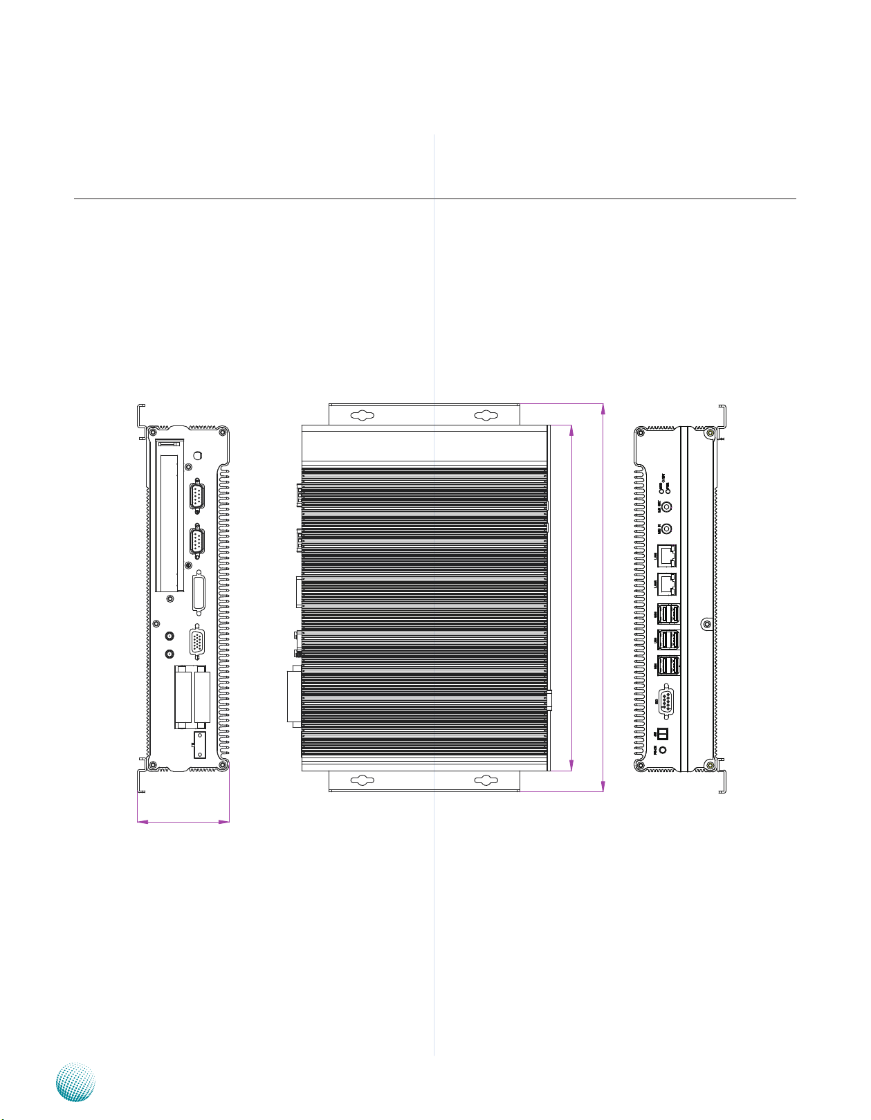
Chapter 2: System Components
System Drawing
Mechanical dimensions of the LEC-2110
Unit: mm
System Components
Embedded and Industrial Computing
6
Page 7
Chapter 2
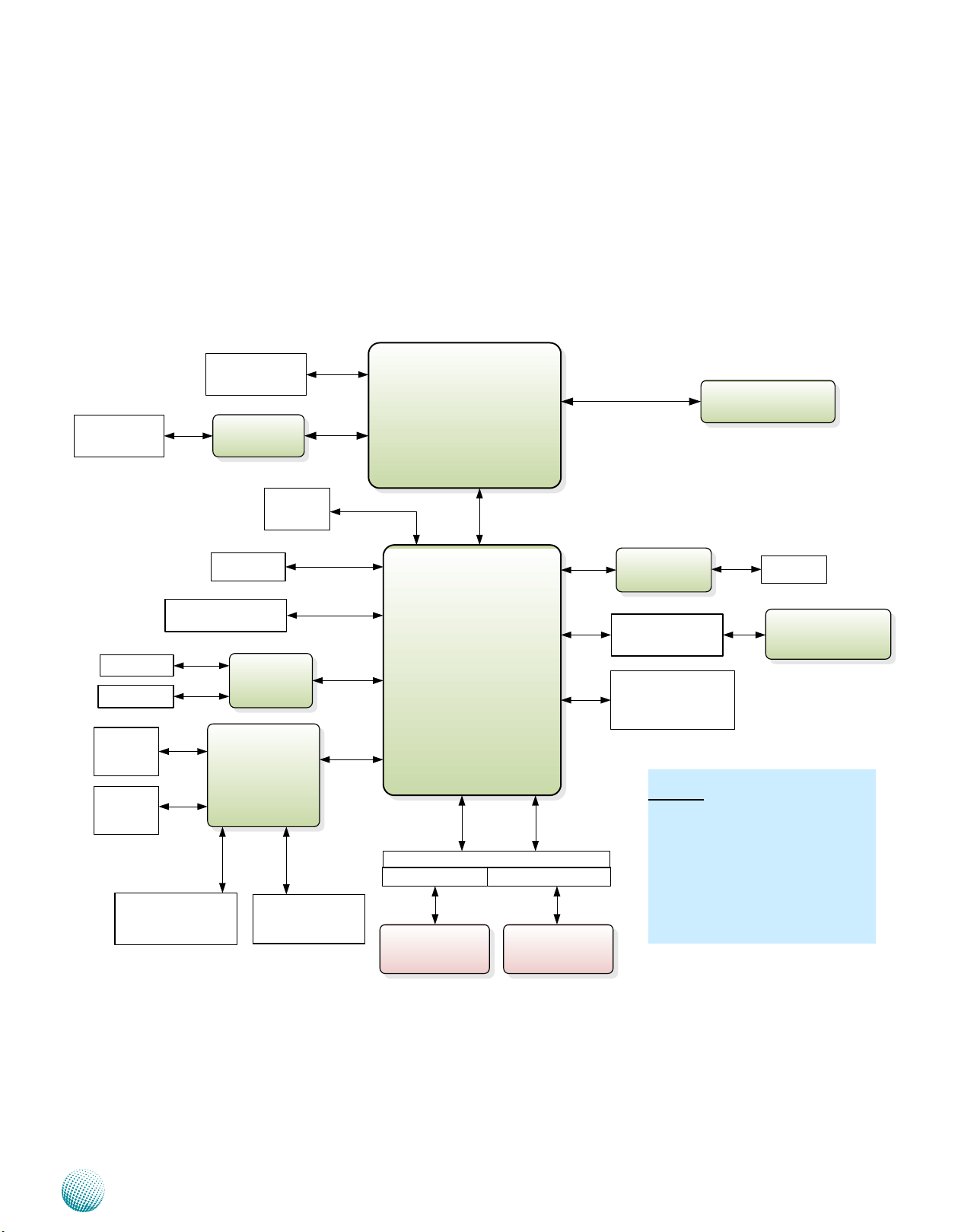
ICH8-M
mBGA
PINEVIEW
ATOM D525
(FCBGA8)
DDR3
1x SO-DIMM up to 4GB
Fintek
F81865F
SATA Port 0
USB
SPI
Mini PCIexpress
Socket
GbE LAN
Realtek
RTL81111E
2x PCIe
2x RJ-45
USB 2.0
6x Port-A (front I/O)
1x Pin Header
SATA Connector
6 Gbps
PCIe
USB 2.0
VGA
Up to 2048x1536
DVI-D
Up to 1920x1080
DVI
SPI ROM
SST 16M
3G Card +
SIM Card Reader
Serial
PCIe
MIC IN
HD Audio
Codec
ALC 888S
Voltage
Thermal
Sensor
Transmitter
CH7036
LVDS
1366 X 768 MAX.
CF Socket
with WOL/PXE
DMI x 4
LPC
Line Out
COM 2/3
RS-232/422/485
with auto-flow Control
LEK-P01*
1X PCI
LEK-E01*
1X PCIexpress 1X
PCI
Gold finger
PCIexpress 1XPCI
PCI PCIe
COM 1/4/5/6
RS-232
Serial
Remark*
The expansion gold finger is flexible
for PCI and PCIe 1X signals;
For LEC-2110, the daughter board
LEK-PO1 or LEK-E01 are selected by
different SKUs.
*LEK- P01 is for LEC-2110P
* LEK-E01 is for LEC-2110E
PS/2
KB/MS
Pin header
Intel Integrated
GMA 3150
Block Diagram
The block diagram depicts the relationships among the
interfaces and modules on the motherboard..
System Components
Embedded and Industrial Computing
7
Page 8
Chapter 2
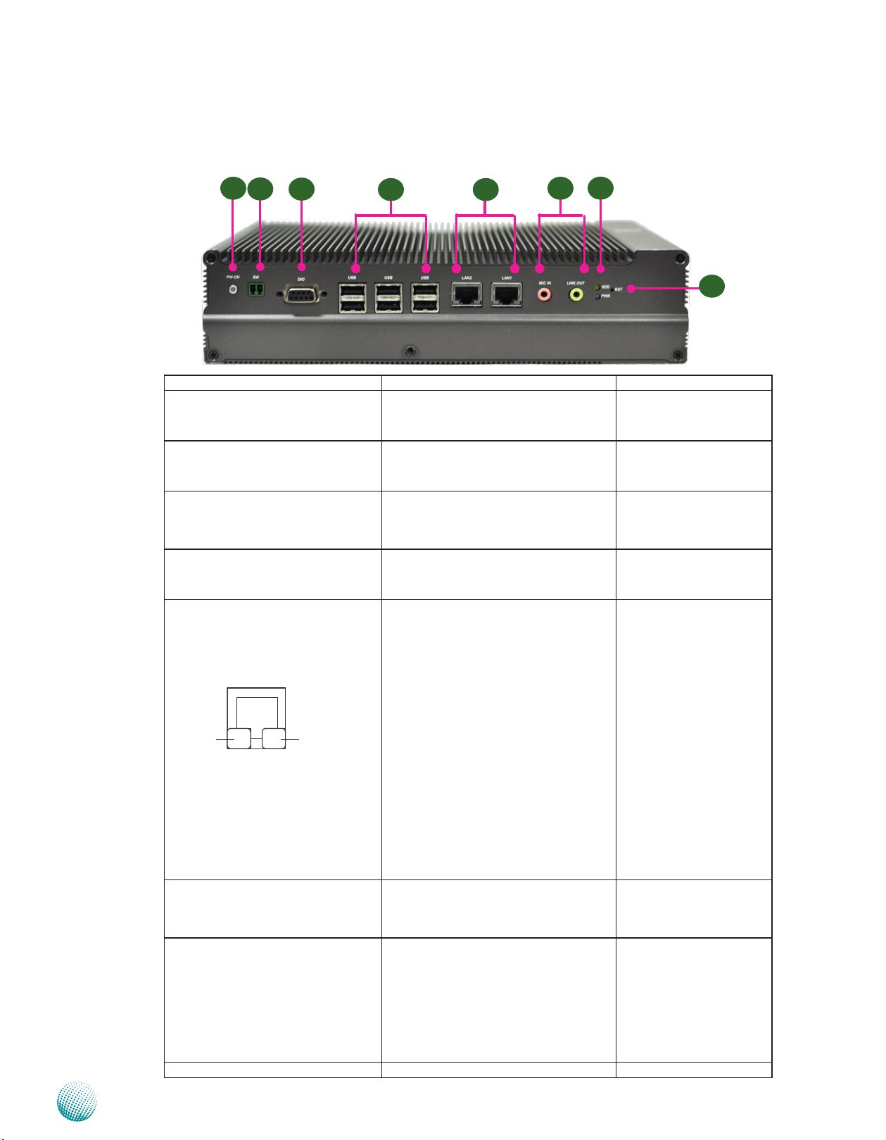
Front Components
System Components
F1
F2
Component Description Pin Definition Reference
F1 Power Button with dual LED ATX Power-on button with LEDs:
F2 Power-on Switch A power-on switch through the
F3 DIO Port A Digital Input/Output port supports 4
F4 Six USB 2.0 Ports An USB type A connector. In addition to
F5 Two 10/100/1000Mbps LAN ports Two RJ-45 (network) jacks with LED
Speed
F6 MIC IN/ LINE OUT Connect the audio devices to these
F7 HDD (Yellow) and
Power LED (Green)
F8 Reset Reset switch
Embedded and Industrial Computing
F3
Link/Active
F4 F5
Standby mode in Red; Power-on mode
in Green
Phoenix contact for distant power-on/
off control
input and 4 output connections. They
are provided by Fintek F81865 super
I/O
this connector, an internal pin header is
provided..
indicators as described below. The LAN
ports are provided by Realtek 8111E.
They both support Wake-on-LAN/
Remote-wake-up.
LINK/ACT (Yellow)
On/Flashing: The port is linking •
and active in data transmission.
Off: The port is not linking.•
SPEED (Green/Amber)
Amber: The connection speed is •
1000Mbps.
Green: The connection speed is •
100Mbps
Off: .The connection speed is •
10Mbps.
ports. The Microphone and line out
port are provided by Realtek ALC
ALC888S
HDD
Blinking: data access activities•
Off: no data access activities•
Power
On: The computer is on.•
Off: The computer is off .•
F6
F7
F8
PSBTN1 on page 15
PSW1 on page 15
DGIO on page 14
Dual USB Port Connectors
on Page 15
LANB1, LANB2 on page
14
MIC1on page 15
LED3 on page 17
8
Page 9
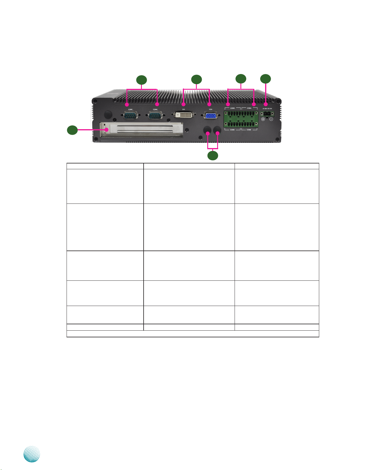
Chapter 2
Rear Components
System Components
R1
R5
Component Description Pin Definition Reference
R1 Two Serial Ports Serial ports through the DB-9
connector; COM1 supports RS-232
and COM2 supports RS-232/422/485
with switch selection among RS232/422/485.
R2 DVI-D/VGA Dual display with the DVI-D (single
link) and VGA ports which are
provided by integrated Graphics
Media Accelerator 3150 through the
Chrontel’s CH7036A LVDS to DVI-D
converter. The displays can support
VGA up to 2048x1536 and DVI-D up
to 1920x1080 respectively.
R3 Four Serial Ports COM3 provide RS232/RS422/RS485
communications with a dip switch
selecting among these standards.
COM4~COM6 provide RS232
communication only.
R4 DC-In (power) Power-in Connector through 1x2
Pin Phoenix Contact Connector.
The LEC-2110 support power range
between +9~+30V DC-in.
R5 Slot for PCI/PCIe expansion
(*)
R6 Antenna Hole Reserved for antenna connection
* Model LEC-2110P supports PCI expansion whereas model LEC-2110E supports PCIe expansion.
The PCIe/PCI expansion capability
is accomplished via the riser card
connected to the system
R2
R6
R3
COM1, COM2 on page 13
DVI1/VGA1 Connectors on page
16/17
CN2 on page 14
CN1 on page 17
PCIGF1/PCIEGF1 ConnectorS on
page 16/17
R4
Embedded and Industrial Computing
9
Page 10
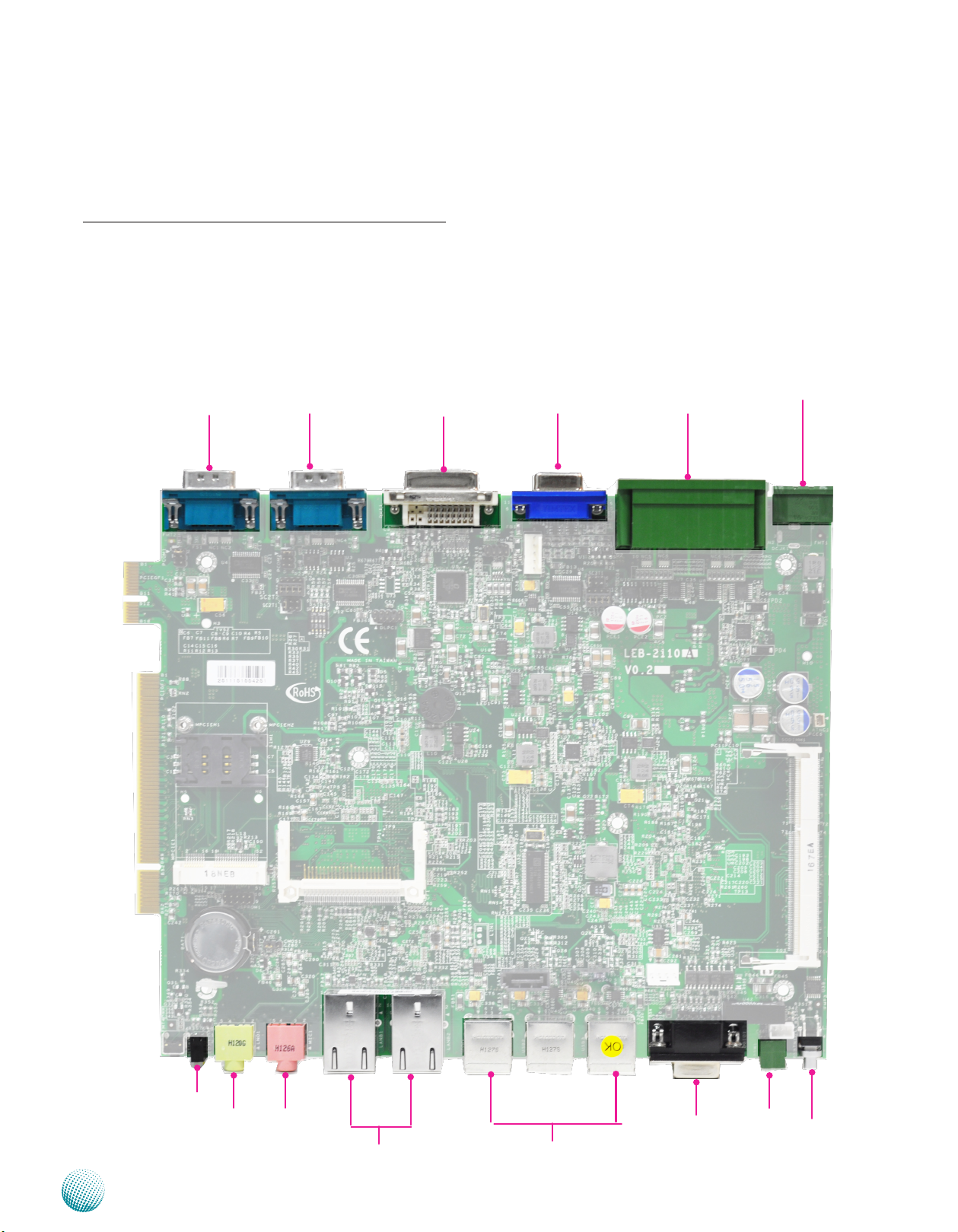
Chapter 3
Chapter 3: Board Layout
External Connectors
The following picture highlights the location of system
input/output connectors. Refer to the table 3.1 Connector
List for more details.
Board Layout
COM1
COM2
DVI1
VGA1
CN2
CN1
LED3
LNO1
Embedded and Industrial Computing
MIC1
LANB1/LANB2
USB1/USB2/USB3
DGIO1
PSW1
PSBTN1
10
Page 11
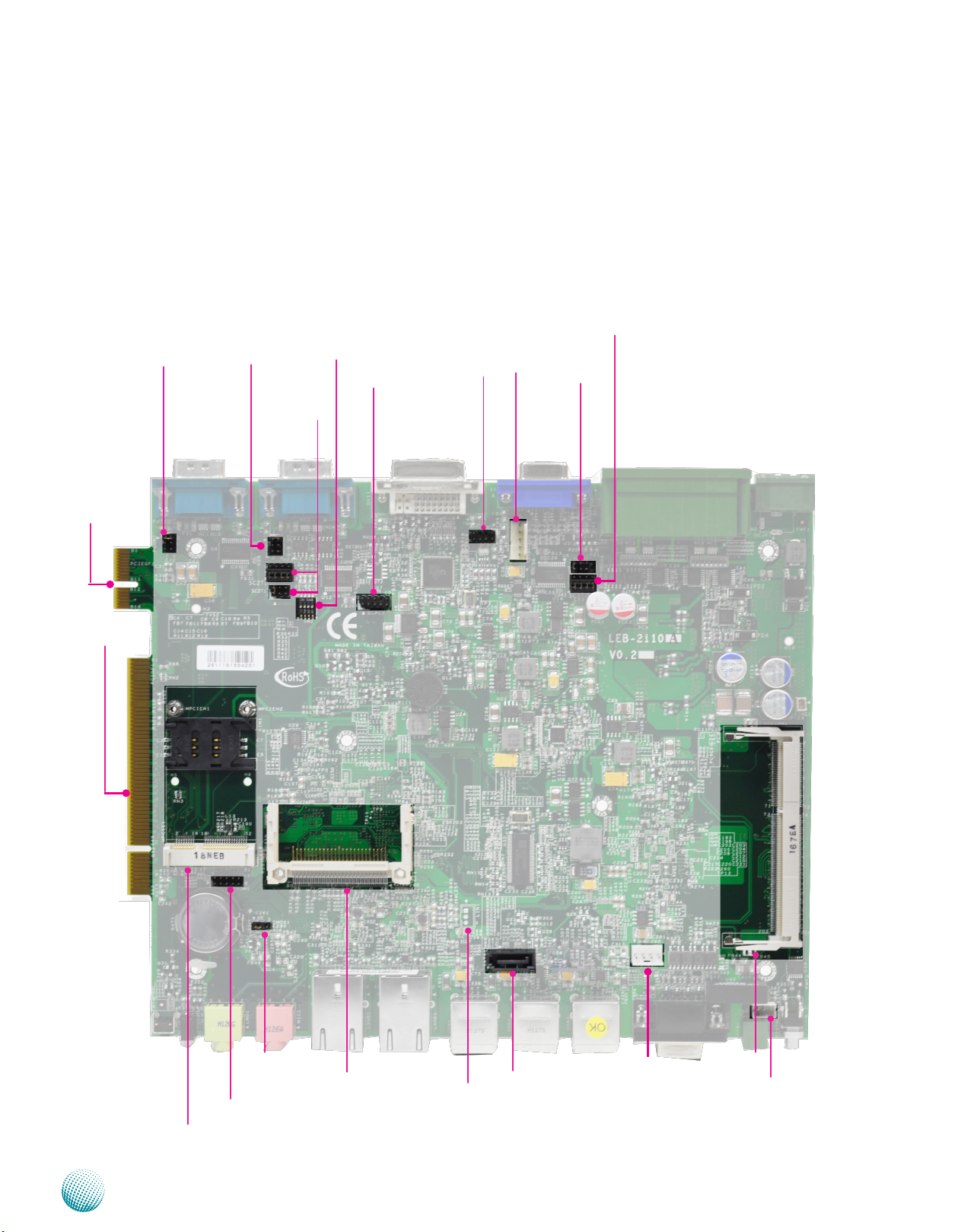
Chapter 3
Internal Connectors and Jumpers
The following picture highlights the location of internal
connectors and jumpers. Refer to the table 3.1 Connector
List for more details.
PCIEGF1
PCOM1
PCOM2
SW2
DLPC1
SC2T2
SC2T1
KM1
USBG1
Board Layout
SC3T2
SC3T1
PCIGF1
MPCIE1
CMOS1
JSPROM1
CF1
LIN1
SATA1
(Reserved for future customization)
PS4S1
SODIMM1
PSW2
LEB-2110A
Embedded and Industrial Computing
11
Page 12

Chapter 3
Board Layout
Connectors and Jumpers List
The tables below list the function of each of the board
jumpers and connectors by labels shown in the above
section. The next section in this chapter gives pin
definitions and instructions on setting jumpers.
Table 3.1 Connector List for LEB-2110A
Labels Function Pin Denition Reference
Page
CF1 CompactFlash Connector P17
CMOS1 Clear CMOS Jumper P14
CN1 DC-in Connector P17
CN2 COM3~COM6 Connector P14
COM1/2 Serial Port COM1/2 Connector P13
DGIO1 Digital Input/Output Connector P14
DLPC1 LPC Port 80 Debug Port Reserved for Factory Use
DVI1 DVI-D Connector P16
JSPROM1 SPI-ROM BIOS Update Port Reserved For Factory Use
KM1 Keyboard/Mouse Connector P17
LANB1/LANB2 RJ45 with 2 LED Indicator LAN Connector P14
LED3 Power and HDD LED P17
LIN1 Line In Connector P15
LNO1 Line Out Connector P15
MIC1 Microphone Port P15
MPCIE1 Mini PCI-Express Connector P15
PCIEGF1 36-Pin Pci-Express Golden Finger P17
PCIGF1 120-Pin PCI Golden Finger P16
PCOM1/2 COM1/COM2 Pin 9 Signal Selection Jumper P13
PS4S1 4-Pin Power Connector P13
PSBTN1 Power-on Push Button with Dual Color LED P15
PSW1 Power-on Switch Connector P15
PSW2 Power-on Switch and Power-on Status Detection Pin Header P17
SATA1/2 SATA Connector P13
SC2T1/SC2T2 COM2 Serial Communication Protocol Selection Jumper P13
SC3T1/SC3T2 COM3 Serial Communication Protocol Selection Jumper P14
SODIMM1 240-Pin SO-DIMM Socket -SW2 COM2/COM3 RS-485 Termination Enabling Jumper P14
USB1~3 Dual USB Connectors P15
USBG1 USB Port Pin Header P15
VGA1 VGA Port P17
Embedded and Industrial Computing
12
Page 13
Chapter 3
Board Layout
Jumper Settings
LEB-2110A
Serial-ATA Connector (SATA1): It is for connecting a 2.5’’
harddisk to be served as your system’s storage. It can
support SATA II which features Data transfer rates up to
3.0 Gb/s (300 MB/s).
Pin No. Function
1 2 3 4 5 6 7
4-pin Serial-ATA Power Connector (PS4S1): It is for
connecting the SATA power cord.
1 2 3 4
1 GND
2 TX+
3 TX4 GND
5 RX6 RX+
7 GND
Pin No. Function
1 +12V
2 GND
3 GND
4 +5V
Pin No. Pin Name
1 DCD TxD- Data2 RXD TxD+ Data+
3 TXD RxD+
4 DTR RxD5 GND
6 DSR
7 RTS
8 CTS
9 RI
RS-232 RS-422 RS-485
SC2T1, SC2T2: Select COM2 Protocol Setting
SC2T1
2
1
6
5
SC2T2
9
5
1
RS-232
12
8
4
RS-232 Serial Port(COM1): It is a RS-232 port through the
D-SUB9 connector.
12345
6789
Pin No. Pin Name Pin No. Pin Name
1 DCD 6 DSR
2 RXD 7 RTS
3 TXD 8 CTS
4 DTR 9 RI
5 GND
Select COM1/COM2 Pin 9 function: Pin 9 of RS-232
port (PCOM1/PCOM2) can be altered according to the
following definition:
1
3
5
2
4
6
Pin No. Function
1-2 (Default) Ring In
3-4 +5V
5-6 +12V
RS-232/422/485 Serial Port (COM2): It is a RS232/422/485 port through the D-SUB9 connector.
12345
6789
Embedded and Industrial Computing
RS-422
RS-485
Switch
Protocol
RS-232
(Default) 1-2
RS-422
RS-485
Note: When using RS-422/RS-485 in COM2, you
must enable the “Serial Port2/3 RS485 driver”
option first in the BIOS menu.
SC2T1 SC2T2
1-5
2-6
3-7
4-8
5-9
3-4
6-10
7-11
8-12
5-9
5-6
6-10
7-11
8-12
13
Page 14

Chapter 3
Board Layout
SW2: Select COM2 and COM3 Termination in RS485 This switch is used to enable or disable the signal
termination for COM2 and COM3. We strongly recommend
that you disable termination when the port is configured
as RS-232 and enable it when the port is configured as RS485/RS-422.
SW2
ON
OFF
COM Port Pin Number Termination
COM2 Selector 1, 2 on/off Enable/Disable
COM3 Selector 3,4 on/off Enable/Disable
The default setting is “Disable”
RS-232/422/485 Serial Port (COM3~COM6, CN2): It has
4 serial ports through terminal block connector. Note that
only COM3 can select among RS232/422/485.
10 9 8 7 6 5 4 3 2 1
COM6 COM5
Note: The orientation
of CN2 illustrated here
is opposite of the one
on the front panel.
COM4 COM3
20 19 18 17 16 15 14 13 12 11
Pin No. Pin Name
RS-232
1 RTS5#
2 RxD5
3 TxD5
4 CTS5#
5 CGND
6 RTS6#
7 RxD6
8 TxD6
9 CTS6#
10 DGND
Pin No. Pin Name
RS-232 RS-422 RS-485
11 RTS3# TX- DATA12 RxD3 TX+ DATA+
13 TxD3 RX+
14 CTS3# RX15 EGND
16 RTS4#
17 RxD4
18 TxD4
19 CTS4#
20 FGND
SC3T1 and SC3T2: Select COM3 Protocol Setting
SC2T1
2
1
6
5
SC2T2
9
5
1
12
8
4
RS-232
Switch
SC3T1 SC3T2
Protocol
RS-232
(Default) 1-2 1-5
2-6
3-7
4-8
RS-422
3-4 5-9
6-10
7-11
8-12
RS-485
5-6 5-9
6-10
7-11
8-12
Note: When using RS-422/RS-485 in COM2, you
must enable the “Serial Port2/3 RS485 driver”
option first in the BIOS menu.
LAN1/LAN2 Ports (LANB1/LANB2): The LAN ports are
provided by RTL8111E-VB-CG Ethernet controller whose
interface complies with PCI-e 1.1 (2.5 Ghz) and IEEE
802.3az Draft 3.0 (EEE). It has advanced management
features including Wake-on-LAN and remote wake-up .
Pin No. Description
Fast Ethernet Gigabit Ethernet
1 TX+ MD0+
2 TX- MD03 RX+ MD1+
4 T45 MD2+
5 T45 MD26 RX- MD17 T78 MD3+
8 T78 MD3-
Clear CMOS jumper (CMOS1): It is for clearing the CMOS
memory.
Pin No. Pin Name
1 2 3
1-2 Normal (Default)
2-3 Clear CMOS
RS-422
RS-485
Embedded and Industrial Computing
Digital I/O (DGIO1)
Digital IN/OUT(DIO1) Connector: The 8 pins of General
Purpose Input/Output (GPIO) support input and output
operations through the DB-9 female connector.
TTL Level is +5V; Maximum input current for each port
is 10mA; Maximum output current for each port is
100uA
Input/Output Voltage Logic Register
0~2V Low 0
2~5V High 1
14
Page 15

Chapter 3
Board Layout
TTL Level is +5V; Maximum input current for each port
is 10mA; Maximum output current for each port is
100uA
The default value is 0
DIO Address
Address Description
0x2eH SUPERIO_INDEX
Digital Input GPIO4, GPIO50~GPIO52
Digital Output GPIO0~GPIO3
5 4 3 2 1
9 8 7 6
Pin No. Pin Name
1 Input0
2 Input1
3 Input2
4 Input3
5 GND
Pin No. Pin Name
6 Output0
7 Output1
8 Output2
9 Output3
Dual USB Port Connector #0 and #1 (USB1):
Dual USB Port Connector #2 and #3 (USB2):
Dual USB Port connector #4 and #5 (USB3):
Pin No. Pin Name
5 6 7 8
1 2 3 4
1 +5V
2 USBD03 USBD0+
4 GND
5 +5V
6 USBD17 USBD1+
8 GND
USB 2.0 Pin Header (USBG1, USB#6):
PIN NO. DESCRIPTION PIN NO. DESCRIPTION
PAD1 Ground PAD2 Ground
1 Ground 3 BUTTON2 Ground 4 BUTTON-
L1 PWR_LED+ /
STB_LED-
L2 PWR_LED- /
STB_LED+
Mini PCI Express Connector (MPCIE1):
Pin No. Description Pin No. Description
1 WAKE# 2 +3.3V
3 RSV1 4 Ground
5 RSV2 6 +1.5V
7 CLKREQ# 8 UIM_PWR
9 Ground 10 UIM_DATA
11 REFCLK- 12 UIM_CLK
13 REFCLK+ 14 UIM_RESET
15 GND3 16 UIM_VPP
17 RSV3 18 Ground
19 RSV4 20 W_DISABLE#
21 GND5 22 PERST#
23 PERn0 24 +3.3V
25 PERp0 26 Ground
27 Ground 28 +1.5V
29 Ground 30 SMB_SLK
31 PETn0 32 SMB_DATA
33 PETp0 34 Ground
35 Ground 36 USB_D-
37 Ground 38 USB_D+
39 +3.3V 40 Ground
41 +3.3V 42 LED_WWAN#
43 Ground 44 LED_WLAN#
45 RSV9 46 LED_WPAN#
47 RSV10 48 +1.5V
49 RSV11 50 Ground
51 RSV12 52 +3.3V
Pin No. Pin Name
5
1 +5V
4
2 USBD6-
3
3 USBD6+
2
4 GND
1
5 NC
Power on Switch through the Phoenix Contact
(PSW1):
Note: The orientation of CN2 illustrated here is opposite of the one on
1 2
the front panel.
PIN NO. DESCRIPTION
1 PWR_BTN_N
2 GND
Power-on Button with dual color (PSBTN1)
1
L1
2
3
L2
4
Line-out Connector through 5-pin jack (LNO1)
Pin No. Description
1 CO_GND
2 LINOUT-L
3 CO_GND
4 LINOUT-JDET
5 LINOUT- R
Microphone Connector through 5-pin jack (MIC1:)
Pin No. Description
1 CO_GND
2 MIC_INL
3 CO_GND
4 MIC-JDET
5 MIC_INR
Line-in (LIN1, reserved for future customization)
1
2
3
Pin No. Description
1 LININ-L
2 CO_GND
3 LININ-R
Embedded and Industrial Computing
15
Page 16

Chapter 3
Board Layout
DVI-D Connector (DVI1): A single link DVI-D Connector
Pin No. Description Pin No. Description
1 TMDS DATA2- 2 TMDS DATA2+
3 TMDS Data 2/4
shield
5 NC 6 DDC_CLK
7 DDC_DATA 8 NC
9 TMDS DATA1- 10 TMDS DATA1+
11 TMDS Data 1/3
shield
13 NC 14 +5V
15 GND 16 HPD
17 TMDS DATA0- 18 TMDS DATA0+
19 TMDS Data 0/5
shield
21 NC 22 TMDS CLK
23 TMDS CLK+ 24 TMDS CLK-
4 NC
12 NC
20 NC
shield
PCI Expansion connector for PCI low prole card (120
pin, PCIGF1)
PIN No. SIDE B SIDE A
1 -12V TRST# (Ground)
2 TCK (Ground) +12V
3 Ground TMS (Ground)
1
4 TDO TDI (Ground)
5 +5V +5V
6 +5V INTA#
7 INTB# INTC#
8 INTD# +5V
62
9 PRSNT1# Reserved
10 Reserved NC (VI/O)
11 PRSNT2# Reserved
12 Ground Ground
13 Ground Ground
14 Reserved 3.3Vaux
15 Ground RST#
16 CLK NC (VI/O)
17 Ground GNT# (GNT-4)
18 REQ# (REQ-4) Ground
19 NC (VI/O) PME#
20 AD31 AD30
21 AD29 +3.3V
22 Ground AD28
23 AD27 AD26
24 AD25 Ground
25 +3.3V AD24
26 C/BE3# IDSEL (AD16)
27 AD23 +3.3V
28 Ground AD22
29 AD21 AD20
30 AD19 Ground
31 +3.3V AD18
PIN No. SIDE B SIDE A
32 AD17 AD16
33 C/BE2# +3.3V
34 Ground FRAME#
35 IRDY# Ground
36 +3.3V TRDY#
37 DEVSEL# Ground
38 Ground STOP#
39 LOCK# +3.3V
40 PERR# SDONE (SMBclk)
41 +3.3V SBO# (SMBdata)
42 SERR# Ground
43 +3.3V PAR
44 C/BE1# AD15
45 AD14 +3.3V
46 Ground AD13
47 AD12 AD11
48 AD10 Ground
49 M66EN (Ground) AD09
50 KEY KEY
51 KEY KEY
52 AD08 C/BE0#
53 AD07 +3.3V
54 +3.3V AD06
55 AD05 AD04
56 AD03 Ground
57 Ground AD02
58 AD01 AD00
59 NC (VI/O) NC (VI/O)
60 ACK64# REQ64#
61 +5V +5V
62 +5V +5V
Embedded and Industrial Computing
16
Page 17

Chapter 3
25 1
50 26
CF1
5
1
Board Layout
PCIe Expansion connector for PCIe low prole card
(36 pin, PCIEGF1)
1
18
PIN No. Side B Side A
1 12V PRSNT1#
2 12V 12V
3 12V 12V
4 Ground Ground
5 SMBCLK JTAG2
6 SMBDATA JTAG3
7 Ground JTAG4
8 +3.3V JTAG5
9 JTAG1 +3.3V
10 +3.3VAUX +3.3V
11 WAKE# PCIE_RESET-
KEY KEY
12 Reserved Ground
13 Ground DEFCLK+
14 PE_TX0+ DEFCLK15 PE_TX0- Ground
16 Ground PE_RX0+
17 PRSNT2# PE_RX018 Ground Ground
DC_IN CONNECTOR (CN1): A Phoenix connector for
external power supply.
1 2
Note: The orientation of CN2 illustrated here is opposite of the one on
the front panel.
Pin No. Pin Name
1 DC_GND
2 DC_IN
Power and HDD LED (LED3)
A1
A2
Pin No. Pin Name PIN No. Pin Name
A1 PWR_LED + C1 PWR_LEDA2 HD_LED+ C2 HD_LED-
C1
C2
VGA Connector (VGA1)
CompactFlash Connector (CF1)
PIN No. Description PIN No. Description
1 GND 26 CD12 DATA3 27 DATA11
29 DATA4 28 DATA12
4 DATA5 29 DATA13
5 DATA6 30 DATA14
6 DATA7 31 DATA15
7 CE1# 32 CE2#
8 A10 33 VS1#
9 OE# 34 IOR#
10 A9 35 IOW#
11 A8 36 WE#
12 A7 37 READY#
13 CFVCC3 38 CFVCC3
14 A6 39 CSEL
15 A5 40 VS2#
16 A4 41 RESET
17 A3 42 WAIT#
18 A2 43 INPACK#
19 A1 44 REG#
20 A0 45 DASP#
21 DATA0 46 DIAG#
22 DATA1 47 DATA8
23 DATA2 48 DATA9
24 WP 49 DATA10
25 CD2- 50 GND
Pin No. Pin Name PIN No. PIN Name PIN No. PIN Name
1 CRT-R 6 GND 11 NC
2 CRT-G 7 GND 12 V_SDAT
3 CRT-B 8 GND 13 HSYNC
4 NC 9 +5V 14 VSYNC
5 GND 10 GND 15 V_SCLK
Power-on Switch and Power-on Status Detection
Connector (PSW2):
Pin No. Pin Name
1 GND
321
2 Power Button3 Detect pwron (+5V)
Keyboard and Mouse Connector (KM1):
7
8
Pin No. Pin Name Pin No. Pin Name
1 +5V 2 MSCLK
3 MSDATA 4 KEY
5 KBDAT 6 KEY
7 GND 8 KBCLK
1
2
Embedded and Industrial Computing
17
Page 18

Chapter 4
Hardware Setup
Chapter 4: Hardware Setup
Preparing the Hardware Installation
To access some components and perform certain service
procedures, you must perform the following procedures
first.
WARNING: To reduce the risk of personal injury,
electric shock, or damage to the equipment,
remove the power cord to remove power from
the server. The power switch button does not
completely shut off system power. Portions of the
power supply and some internal circuitry remain
active until AC power is removed.
Unpower the LEC-2110 and remove the power cord.1.
Turn the device upside down.2.
Unscrew 6 screws on the bottom chassis. And unscrew 3.
the 3screws from both the front and back panel.
Bent the front panel slightly to lift the cover4.
Installing the System Memory
The motherboard supports DDR3 memory to meet the
higher bandwidth requirements of the latest operating
system and applications. It comes with one Double Data
Rate Three (DDR3) Small Outline Dual Inline Memory
Module (DDR3 SO-DIMM) socket.
Align the memory module’s cutout with the SO-DIMM 1.
socket’s notch.
Install the SO-DIMM.2.
1
2
3
Open the cover.5.
4 5
Note:
3
2
The system can support memory of DDR3 1.
SO-DIMM DDR3 800 MHz up to 4 GB in
maximum.
To release the memory, bent the latch slightly 2.
outward.
Embedded and Industrial Computing
18
Page 19
Chapter 4
Hardware Setup
3G SIM Card Installation
Unlink the SIM card reader first by sliding it outward.1.
Flip the SIM card reader diagonally.2.
Align the cut corner of the SIM card with the cut corner 3.
of SIM card reader. Make sure the ICs will be in contact
with the SIM card reader.
Insert the 4. SIM card into the reader and close the tray.
You should feel a click when the SIM card is locked
securely in the SIM card reader.
Wireless Module Installation
Align the wireless module’s cutout with the Mini-PCIe 1.
slot notch.
Insert the wireless module into the connector 2.
diagonally.
Push the other end of the wireless module to be 3.
tightened with the latch.
2
4
PCI/PCIe Riser Card Installation
The system can accommodate one PCI or PCIe expansion
(only one of them at a time) module. In order the install
the PCI or PCIe expansion module, a low-profile riser card
has to be installed first. Follow these steps to install the
riser card:
Fix the riser card on the bracket with 2 screws.1.
Install the riser card on the system by connecting the 2.
connectors with the system’s PCI/PCIE connector. Due
to space constraint, align the card with the connector
with a 45 degree angle and gradually push the card
down while inserting the card.
Fix the riser card on the board.3.
1
PCI
PCIe
3
2
3
PCI
2
Open
Cut
Corner
Lock
Note: To remove the SIM card, push the card
outward to unlock it.
Embedded and Industrial Computing
19
Page 20

Chapter 4
2
Hardware Setup
PCIe
PCI
3
PCIe
Embedded and Industrial Computing
20
Page 21

Chapter 4
Hardware Setup
Installing the Hard Disk
The system can accommodate one Serial-ATA disk. Follow
these steps to install a hard disk into the system:
Put hard disk on the bottom chassis and fix the hard disk 1.
on the chassis with 4 mounting screws as illustrated in
the following picture.
Plug the Serial-ATA cable to the hard disk.2.
Connect the Serial-ATA power and data disk cables to 3.
the Serial-ATA power and disk connectors on the main
board respectively.
Close the cover and fix it firmly to the system with the 4.
screws.
1
Note: Using a PCIe or PCI riser card, users have
choice of either PCI or PCI Express 1x expansion:
1x PCI can be supported by model LEC-2110P1.
1x PCIe can be supported by model LEC-2110E2.
Both of PCI or PCIe support the Max. 3.
Dimension as the following illustrated and the
Max. PowerPower consumption reserved for
expansion is 10W.
2
3
Embedded and Industrial Computing
21
Page 22
Chapter 4
268
190
64
7
100
100
283
14
96
301
71
118
39
36
Hardware Setup
Connecting Power
Connect the LEC-2110 to a +9~+30V DC-in power source.
The DC power-in connector comes with a 2-pin terminal
block for its Phoenix contact. This power socket can only
accept the power supply with the right pin contact so be
cautious when inserting power to the system.
DC IN
+ -
Wall Mounting
The product ships with wall mounting kit. To mount your
product on the wall, follow the instructions below:
First make a hole for the anchor in the surface on the 1.
wall. Use the following diagram as a guideline for
placing the anchors.
Then press the anchor into the hole until it is flush with 2.
the surface. You may need a hammer to tap the wall
anchor.
Use a screwdriver to screw the threaded screw into the 3.
plastic anchor.
Attach the wall mounting bracket to the back of the 4.
device, securing it in place with four of the flat-head
screws provided.
Hang the device on the wall.5.
Embedded and Industrial Computing
Unit: mm
22
Page 23
Appendix A
Programming Watchdog Timer
Appendix A: Programming Watchdog Timer
A watchdog timer is a piece of hardware that can be
used to automatically detect system anomalies and reset
the processor in case there are any problems. Generally
speaking, a watchdog timer is based on a counter that
counts down from an initial value to zero. The software
selects the counter’s initial value and periodically restarts
it. Should the counter reach zero before the software
restarts it, the software is presumed to be malfunctioning
and the processor’s reset signal is asserted. Thus, the
processor will be restarted as if a human operator had
cycled the power.
For sample watchdog code, see Watch dog and DIO folder
in the Driver and Manual CD
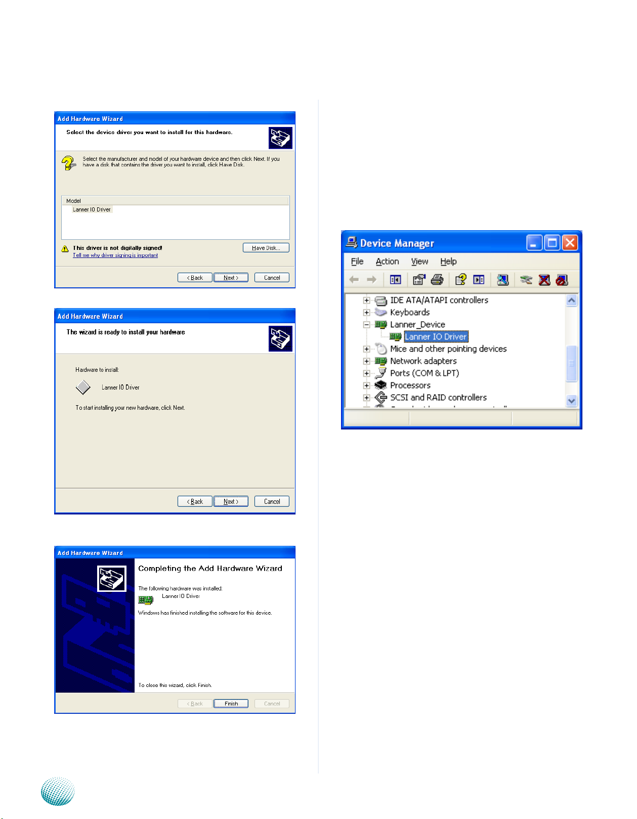
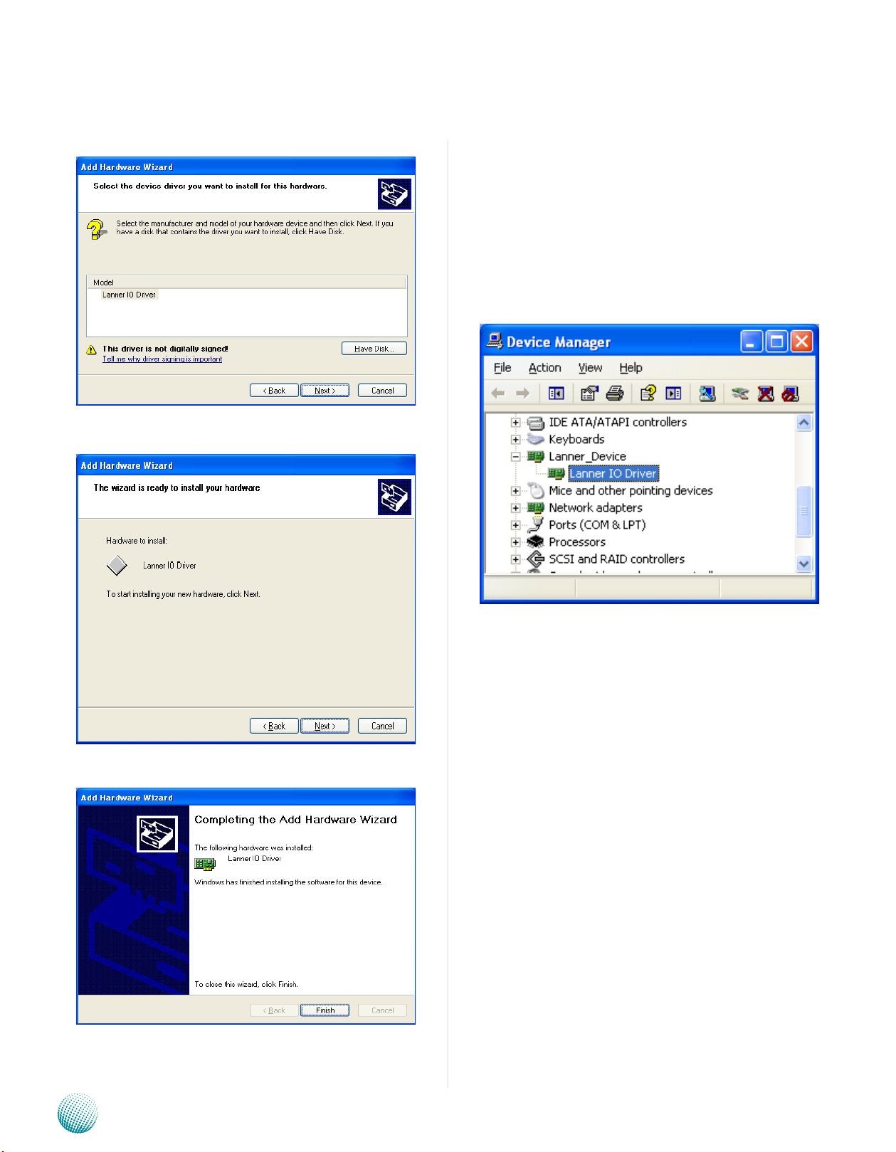
Click Next to proceed5.
Answer “Yes” to the question and select Next to 6.
proceed.
Driver Installation
Before you could access or control the operation of the
watchdog and Digital I/O functions, install the the L_IO
driver which is the library and driver needed for Lanner
General Purpose Input/Output interface or functions.
To install the L_IO driver:
Restart the computer, and then log on with 1.
Administrator privilege.
Insert the Drivers and User’s Manual CD to the USB-2.
optical drive.
Browse the contents of the support CD to locate the 3.
file LIO.rar under the \Watch dog and DIO\LIO folder
and unzip the file.
From the control panel, click the ADD Hardware 4.
program
Select Add a new hardware device.7.
Embedded and Industrial Computing
23
Page 24
Appendix A
Programming Watchdog Timer
Choose to select the hardware Manually8.
Choose Show all device and click Next.9.
Click HaveDisk to locate the L_IO.inf file11.
Select the L_IO.inf12.
Click HaveDisk to locate the L_IO.inf file10.
Embedded and Industrial Computing
Select OK to confirm with the installation13.
24
Page 25
Appendix A
Programming Watchdog Timer
Select the Lanner IO driver and click Next.14.
Click Next15.
To verify the GPIO driver installation, do the following
steps:
Right-click on the My Computer icon, and then select 1.
Properties form the menu.
Click the Hardware tab, then click the Device Manager 2.
button.
Click the + sign next to the Lanner_Device, then the 3.
Lanner IO Driver should be listed.
Click 16. Complete to close the installation program.
Embedded and Industrial Computing
25
Page 26

Appendix A
Programming Watchdog Timer
On Linux
Executing the commands through the Command Line:
1. wd_tst --swtsr (Set Watchdog Timeout State to Reset)
2. wd_tst --swt xxx (Set Watchdog Timer 1-255 seconds)
3. wd_tst[*] --start (Start Watchdog Timer)
4. wd_tst --stop (Stop Watchdog Timer)
The following procedures are required for running the
watchdog program on DOS, Linux and FreeBSD.
Note:
For DOS environment, use DJGPP as compiler 4.
and the makefile: Makefile.dos.
For Linux, support kernel versions are 2.4.x and 5.
2.6.x. Use the makefile:Makefile.linux.
For FreeBSD, support version is FreeBSD 8.0. 6.
Use the makefile: Makefile.
Build
To build program source code on Linux platform, use the
following steps as a guideline:
Insert module and create node in /dev as below
example:
#insmod wd_drv.[k]o
#mknod /dev/wd_drv c 241 0
For FreeBSD:
Insert module as below example:
#kldload -v ./wd_drv.ko
Execute
# wd_tst --swtsb (Set Watchdog Timeout State to Bypass
function)
# wd_tst --swtsr (Set Watchdog Timeout State to Reset
function)
# wd_tst --swt xxx (Set Watchdog Timer 1-255 seconds)
# wd_tst[*] --start (Start Watchdog Timer)
# wd_tst --stop (Stop Watchdog Timer)
Note:
Copy the proper makefile from the Driver and Manual 1.
CD to your system
Set the access mode with these two parameters 2.
by editing the Makefile.linux directly: DIRECT_IO_
ACCESS= [0|1] (enter either 1 or 0) and LANNER_
DRIVER= [0|1] (enter either 1 or 0). 1 is for direct access
and no driver is needed. You will only need to execute
the program directly. However, when it equaled to 0,
driver installation is needed. Refer to the following
Install section for more details.
Type make to build source code:3.
make Makefile (Note: omit the file extensions)
After compiled, the executable program (bpwd_tst) and
the driver (bpwd_drv.ko) will be in the bin subdirectory.
Install
The installation procedures depend on the access mode
that you have set by using the above mentioned method.
If you have set DIRECT_IO_ACCESS=1, driver installation is
not necessary. Proceed to the next section on executing
If you have set DIRECT_IO_ACCESS=0, Lanner bypass
driver needs to be installed. Install the driver and create
a node in the /dev directory as shown in the following
example:
wd_tst --start will not be available if 1.
DIRECT_IO_ACCESS=1, use the command: “./
wd_tst --swt xxx” to start the watchdog timer
instead .
Watchdog timer can support two functions, 2.
- system rest or LAN bypass. However, only
one function can be activated at a time. You
should modify the code or switch it to the
desired state/function accordingly.
For more details, refer to the README file 3.
contained within the program.
For Linux:
Embedded and Industrial Computing
26
Page 27

Appendix A
Programming Watchdog Timer
Watch Dog sample code:
#include “../include/config.h”
#include “../include/version.h”
/* standard include file */
#include <stdio.h>
#include <stdlib.h>
#include <unistd.h>
#ifdef DJGPP
/* For DOS DJGPP */
#include <dos.h>
#include <inlines/pc.h>
#include <stdint.h>
#include <fcntl.h>
#include <errno.h>
#include <string.h>
#include “../include/wd_ioctl.h”
#define delay(x) usleep(x)
#ifdef DIRECT_IO_ACCESS
#warning ***** Note: You build with DIRECT_IO_ACCESS
defined *****
#warning ***** Note: undefine this to build for driver code
*****
#endif
#endif
/* local include file */
#ifndef DIRECT_IO_ACCESS
#error ***Error: define DIRECT_IO_ACCESS in config.h for
DOS ***
#endif
#else
/* For Linux */
#if defined(LINUX_ENV)
#include <sys/io.h>
#endif
#if defined(FreeBSD_ENV)
#define SET_IOPL() (iofl=open(“/dev/io”,000))
#define RESET_IOPL() close(iofl)
#include <machine/cpufunc.h>
#endif
#include “../include/ioaccess.h”
#ifndef BYPASS_PAIR_NUMBER
#error “You should defined PAIR_NUMBER in include/
config.h”
#endif
#if BYPASS_PAIR_NUMBER == 1
char pair_str[16]=”[1]”;
#endif
#if BYPASS_PAIR_NUMBER == 2
char pair_str[16]=”[1|2]”;
#endif
#if BYPASS_PAIR_NUMBER == 3
char pair_str[16]=”[1|2|3]”;
#endif
#include <time.h>
Embedded and Industrial Computing
#if BYPASS_PAIR_NUMBER == 4
char pair_str[16]=”[1|2|3|4]”;
27
Page 28

Appendix A
Programming Watchdog Timer
#endif
#if BYPASS_PAIR_NUMBER == 5
char pair_str[16]=”[1|2|3|4|5]”;
#endif
void print_usage(char* argv0)
{
#if BYPASS_PAIR_NUMBER > 0
printf(“%s --srbe %s (Set Pair %s Runtime Bypass
Enabled)\n”, argv0, pair_str, pair_str);
printf(“%s --srbd %s (Set Pair %s Runtime Bypass
Disabled)\n”, argv0, pair_str, pair_str);
printf(“%s --sobe %s (Set Pair %s Off-mode Bypass
Enabled)\n”, argv0, pair_str, pair_str);
printf(“%s --sobd %s (Set Pair %s Off-mode Bypass
Disabled)\n”, argv0, pair_str, pair_str);
printf(“%s --swtsb (Set Watchdog Timeout State to
Bypass)\n”, argv0);
utility ===\n”);;
fprintf(stdout, PLATFORM_NAME” Watchdog/
Bypass “CODE_VERSION”\n\n”);;
if ( argc < 2) {
print_usage(argv[0]);
return -1;
}
#if ( defined(DIRECT_IO_ACCESS) && !defined(DJGPP) )
#if defined(LINUX_ENV)
iopl(3);
#endif
#if (defined(FreeBSD_ENV))
int iofl;
SET_IOPL();
#endif
#endif
printf(“%s --swtsr (Set Watchdog Timeout State to
Reset)\n”, argv0);
#endif
#if ( defined(DIRECT_IO_ACCESS) )
printf(“%s --swt xxx (Set Watchdog Timer 1-255 seconds
and start to count-down)\n”, argv0);
#else
printf(“%s --swt xxx (Set Watchdog Timer 1-255 seconds)\n”,
argv0);
printf(“%s --start (Start Watchdog Timer)\n”, argv0);
#endif
printf(“%s --stop (Stop Watchdog Timer)\n”, argv0);
}
int main( int argc, char** argv )
{
int devfd;
int value;
#ifdef DIRECT_IO_ACCESS
wd_gpio_init();
#else
devfd = open(“/dev/wd_drv”, O_RDONLY);
if(devfd == -1)
{
printf(“Can’t open /dev/wd_drv\n”);
return -1;
}
#endif
/******** set watchdog timer count ***********************
****************/
if ( !strcmp(argv[1], “--swt”)) {
int tmp;
if (argc !=3) {
printf(“No timer input, program terminated\n”);
close(devfd);
exit -1;
fprintf(stdout, “=== Lanner platform miscellaneous
Embedded and Industrial Computing
}
tmp = atoi(argv[2]);
28
Page 29

Appendix A
Programming Watchdog Timer
if ( (tmp < 1) || (tmp > 255)) {
printf(“Wrong timer value, please input within
(1~255)\n”);
close(devfd);
exit -1;
}
printf(“Set Watchdog Timer....”);
#if defined(DIRECT_IO_ACCESS)
start_watchdog_timer(tmp);
printf(“OK\n”);
#else
if( ioctl(devfd, IOCTL_SET_WDTO_TIMER, &tmp) != 0)
printf(“Fail\n”);
else
printf(“OK\n”);
#endif
}
/******** Start watchdog timer ***************************
****************/
#if !defined(DIRECT_IO_ACCESS)
else if ( !strcmp(argv[1], “--start”)) {
printf(“Start Watchdog Timer....”);
value = START_WDT;
if( ioctl(devfd, IOCTL_START_STOP_WDT, &value) !=
0)
0)
printf(“Fail\n”);
else
printf(“OK\n”);
#endif
}
#if BYPASS_PAIR_NUMBER > 0
/******** Set lan-bypass enable while watchdog timer
expired *************/
else if ( !strcmp(argv[1], “--swtsb”)) {
printf(“Set Watchdog Timeout State to Lan
Bypass....”);
#if defined(DIRECT_IO_ACCESS)
set_wdto_state_system_bypass();
printf(“OK\n”);
#else
value = SET_WDTO_STATE_LAN_BYPASS;
if( ioctl(devfd, IOCTL_SET_WDTO_STATE, &value) !=
0)
printf(“Fail\n”);
else
printf(“OK\n”);
#endif
}
printf(“Fail\n”);
else
printf(“OK\n”);
}
#endif
/******** Stop watchdog timer ***************************
*****************/
else if ( !strcmp(argv[1], “--stop”)) {
printf(“Stop Watchdog Timer....”);
#if defined(DIRECT_IO_ACCESS)
stop_watchdog_timer();
printf(“OK\n”);
#else
value = STOP_WDT;
if( ioctl(devfd, IOCTL_START_STOP_WDT, &value) !=
Embedded and Industrial Computing
/******** Set system reset while watchdog timer expired
******************/
else if ( !strcmp(argv[1], “--swtsr”)) {
printf(“Set Watchdog Timeout State to System
Reset....”);
#if defined(DIRECT_IO_ACCESS)
set_wdto_state_system_reset();
printf(“OK\n”);
#else
value = SET_WDTO_STATE_SYSTEM_
RESET;
if( ioctl(devfd, IOCTL_SET_WDTO_STATE, &value) !=
0)
printf(“Fail\n”);
else
printf(“OK\n”);
29
Page 30

Appendix A
Programming Watchdog Timer
#endif
}
/******** Set runtime bypass enable **********************
****************/
else if ( (!strcmp(argv[1], “--srbe”)) && (argc==3)) {
if ( !strcmp(argv[2],”1”) ) {
value = BYPASS_PAIR_1;
#if BYPASS_PAIR_NUMBER > 1
} else if (!strcmp(argv[2],”2”) ) {
value = BYPASS_PAIR_2;
#if BYPASS_PAIR_NUMBER > 2
} else if (!strcmp(argv[2],”3”) ) {
value = BYPASS_PAIR_3;
#if BYPASS_PAIR_NUMBER > 3
} else if (!strcmp(argv[2],”4”) ) {
value = BYPASS_PAIR_4;
#endif //DIRECT_IO_ACCESS
} //--srbe
/******** Set runtime bypass enable **********************
****************/
else if ( (!strcmp(argv[1], “--srbd”)) && (argc==3)) {
if ( !strcmp(argv[2],”1”) ) {
value = BYPASS_PAIR_1;
#if BYPASS_PAIR_NUMBER > 1
} else if (!strcmp(argv[2],”2”) ) {
value = BYPASS_PAIR_2;
#if BYPASS_PAIR_NUMBER > 2
} else if (!strcmp(argv[2],”3”) ) {
value = BYPASS_PAIR_3;
#if BYPASS_PAIR_NUMBER > 3
} else if (!strcmp(argv[2],”4”) ) {
value = BYPASS_PAIR_4;
#if BYPASS_PAIR_NUMBER > 4
#if BYPASS_PAIR_NUMBER > 4
} else if (!strcmp(argv[2],”5”) ) {
value = BYPASS_PAIR_5;
#endif //>4
#endif //>3
#endif //>2
#endif //>1
} else {
printf(“Wrong pair number\n”);
return -1;
}
printf(“Set Runtime Bypass Enable....”);
#if defined(DIRECT_IO_ACCESS)
set_runtime_bypass_enable(value);
printf(“OK\n”);
#else
value |= RUNTIME_BYPASS_STATE_ENABLE;
if( ioctl(devfd, IOCTL_RUNTIME_BYPASS_STATE, &value)
!= 0)
} else if (!strcmp(argv[2],”5”) ) {
value = BYPASS_PAIR_5;
#endif //>4
#endif //>3
#endif //>2
#endif //>1
} else {
printf(“Wrong pair number\n”);
return -1;
}
printf(“Set Runtime Bypass Disable....”);
#if defined(DIRECT_IO_ACCESS)
set_runtime_bypass_disable(value);
printf(“OK\n”);
#else
value |= RUNTIME_BYPASS_STATE_DISABLE;
if( ioctl(devfd, IOCTL_RUNTIME_BYPASS_STATE, &value)
!= 0)
printf(“Fail\n”);
printf(“Fail\n”);
else
printf(“OK\n”);
Embedded and Industrial Computing
else
printf(“OK\n”);
#endif //DIRECT_IO_ACCESS
30
Page 31

Appendix A
Programming Watchdog Timer
} //--srbd
/******** Set system-off bypass enable ********************
***************/
else if ( (!strcmp(argv[1], “--sobe”)) && (argc==3)) {
if ( !strcmp(argv[2],”1”) ) {
value = BYPASS_PAIR_1;
#if BYPASS_PAIR_NUMBER > 1
} else if (!strcmp(argv[2],”2”) ) {
value = BYPASS_PAIR_2;
#if BYPASS_PAIR_NUMBER > 2
} else if (!strcmp(argv[2],”3”) ) {
value = BYPASS_PAIR_3;
#if BYPASS_PAIR_NUMBER > 3
} else if (!strcmp(argv[2],”4”) ) {
value = BYPASS_PAIR_4;
#if BYPASS_PAIR_NUMBER > 4
} //--sobe
/******** Set system-off bypass disable *******************
***************/
else if ( (!strcmp(argv[1], “--sobd”)) && (argc==3)) {
if ( !strcmp(argv[2],”1”) ) {
value = BYPASS_PAIR_1;
#if BYPASS_PAIR_NUMBER > 1
} else if (!strcmp(argv[2],”2”) ) {
value = BYPASS_PAIR_2;
#if BYPASS_PAIR_NUMBER > 2
} else if (!strcmp(argv[2],”3”) ) {
value = BYPASS_PAIR_3;
#if BYPASS_PAIR_NUMBER > 3
} else if (!strcmp(argv[2],”4”) ) {
value = BYPASS_PAIR_4;
#if BYPASS_PAIR_NUMBER > 4
} else if (!strcmp(argv[2],”5”) ) {
value = BYPASS_PAIR_5;
#endif //>4
#endif //>3
#endif //>2
#endif //>1
} else {
printf(“Wrong pair number\n”);
return -1;
}
printf(“Set System-Off Bypass Enable....”);
#if defined(DIRECT_IO_ACCESS)
set_bypass_enable_when_system_off(value);
printf(“OK\n”);
#else
value |= SYSTEM_OFF_BYPASS_STATE_ENABLE;
if( ioctl(devfd, IOCTL_SYSTEM_OFF_BYPASS_STATE,
&value) != 0)
} else if (!strcmp(argv[2],”5”) ) {
value = BYPASS_PAIR_5;
#endif //>4
#endif //>3
#endif //>2
#endif //>1
} else {
printf(“Wrong pair number\n”);
return -1;
}
printf(“Set System-Off Bypass Disable....”);
#if defined(DIRECT_IO_ACCESS)
set_bypass_disable_when_system_off(value);
printf(“OK\n”);
#else
value |= SYSTEM_OFF_BYPASS_STATE_DISABLE;
if( ioctl(devfd, IOCTL_SYSTEM_OFF_BYPASS_STATE,
&value) != 0)
printf(“Fail\n”);
else
printf(“OK\n”);
#endif //DIRECT_IO_ACCESS
Embedded and Industrial Computing
printf(“Fail\n”);
else
printf(“OK\n”);
#endif //DIRECT_IO_ACCESS
31
Page 32

Appendix A
} //--sobe
#endif //>0
else {
printf(“<<<Error: Unknown
Parameter>>>\n”);
print_usage(argv[0]);
return -1;
}
#ifdef DIRECT_IO_ACCESS
#if (defined(FreeBSD_ENV))
RESET_IOPL();
#endif
Programming Watchdog Timer
#else
close(devfd);
#endif
return 0;
}
Embedded and Industrial Computing
32
Page 33

Appendix B
Digital Input/Output Control
Appendix B: Digital Input/Output Control on the GPIO port
The Digitanl I/O on the rear panel is designed to provide
the input and output operations for the system. For
sample DIO code, see Watch dog and DIO in the Driver and
Manual CD.
On Windows
Driver Installation
Before you could access or control the operation of the
watchdog and Digital I/O functions, install the the L_IO
driver which is the library and driver needed for Lanner
General Purpose Input/Output interface or functions.
To install the L_IO driver:
Restart the computer, and then log on with 1.
Administrator privilege.
Click Next to proceed5.
Answer “Yes” to the question and select Next to 6.
proceed.
Insert the Drivers and User’s Manual CD to the USB-2.
optical drive.
Browse the contents of the support CD to locate the 3.
file LIO.rar under the \Watch dog and DIO\LIO folder
and unzip the file.
From the control panel, click the ADD Hardware 4.
program
Select Add a new hardware device.7.
Embedded and Industrial Computing
33
Page 34

Appendix B
Digital Input/Output Control
Choose to select the hardware Manually8.
Choose Show all device and click Next.9.
Click HaveDisk to locate the L_IO.inf file11.
Select the L_IO.inf12.
Click HaveDisk to locate the L_IO.inf file10.
Embedded and Industrial Computing
Select OK to confirm with the installation13.
34
Page 35
Appendix B
Digital Input/Output Control
Select the Lanner IO driver and click Next.14.
Click Next15.
To verify the GPIO driver installation, do the following
steps:
Right-click on the My Computer icon, and then select 1.
Properties form the menu.
Click the Hardware tab, then click the Device Manager 2.
button.
Click the + sign next to the Lanner_Device, then the 3.
Lanner IO Driver should be listed.
Click 16. Complete to close the installation program.
Embedded and Industrial Computing
35
Page 36

Appendix B
Digital Input/Output Control
On Linux
Executing the commands through the Command Line:
# dio_tst
The program will drive output pin with specific value and
read status of input pin. If you have external loopback
which connects input to output pins directly, the input
value should be identical with the output value.
Note:
For DOS environment, use DJGPP as compiler 4.
and the makefile: Makefile.dos.
For Linux, support kernel versions are 2.4.x and 5.
2.6.x. Use the makefile:Makefile.linux.
For FreeBSD, support version is FreeBSD 8.0. 6.
use the makefile: Makefile.
Build
To build program source code on Linux platform, use the
following steps as a guideline:
Install
The installation procedures depend on the access mode
that you have set by using the above mentioned method.
If you have set DIRECT_IO_ACCESS=1, driver installation is
not necessary. Proceed to the next section on executing
If you have set DIRECT_IO_ACCESS=0, Lanner bypass
driver needs to be installed. Install the driver and create
a node in the /dev directory as shown in the following
example:
For Linux:
Insert module and create node in /dev as below
example:
#insmod dio_drv.[k]o
#mknod /dev/dio_drv c 240 0
For FreeBSD:
Insert module as below example:
#kldload -v ./dio_drv.ko
Copy the proper makefile from the Driver and Manual 1.
CD to your system
Set the access mode with these two parameters 2.
by editing the Makefile.linux directly: DIRECT_IO_
ACCESS= [0|1] (enter either 1 or 0) and LANNER_
DRIVER= [0|1] (enter either 1 or 0). 1 is for direct access
and no driver is needed. You will only need to execute
the program directly. However, when it equaled to 0,
driver installation is needed. Refer to the following
Install section for more details.
Type make to build source code:3.
make Makefile (Note: omit the file extensions)
After compiled, the executable program (bpwd_tst) and
the driver (bpwd_drv.ko) will be in the bin subdirecto
I/O Address
DIO Address
Address Description
0x2e SUPERIO_INDEX
0x2f SUPERIO_DATA
GPIO4,
GPIO50~GPIO52
GPIO0~GPIO3 Digital Output
Execute
Once build completed, application (and driver) is available
in bin sub-directory.
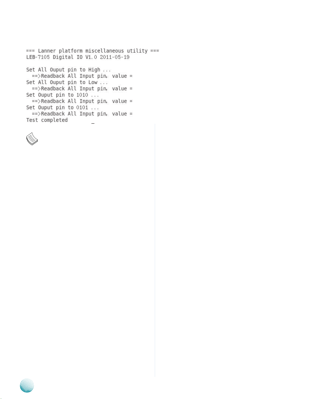
Just run “dio_tst” for Digital IO test. This program will drive
output pin with specific value and read status of input
pin. If you have external loopback which connects input
to output pins directly, the input value should be identical
with output value.
screen capture of the execution result:
Digital Input
Embedded and Industrial Computing
36
Page 37
Appendix B
Digital Input/Output Control
#include “../include/config.h”
#ifdef DJGPP
/* standard include file */
#include <stdio.h>
#include <stdlib.h>
#include <unistd.h>
Note: For more details, refer to the README file
contained within the program
/* For DOS DJGPP */
#include <dos.h>
#include <inlines/pc.h>
#else //DJGPP
/* For Linux */
#ifdef DIRECT_IO_ACCESS
/* For Linux direct io access code */
/* standard include file */
#include <stdio.h>
#include <stdlib.h>
#include <unistd.h>
#if defined(LINUX_ENV)
#include <sys/io.h>
Embedded and Industrial Computing
#endif
#if defined(FreeBSD_ENV)
#include <machine/cpufunc.h>
#endif
#include <time.h>
#include <stdint.h>
#include <fcntl.h>
#include <errno.h>
37
Page 38

Appendix B
#include <string.h>
Digital Input/Output Control
#define delay(x) usleep(x)
#endif
#ifdef MODULE
#include <linux/kernel.h>
#include <linux/module.h>
#include <linux/kernel.h>
#include <linux/fs.h>
#include <asm/io.h>
#include <linux/delay.h>
#undef delay
#define delay(x) mdelay(x)
#undef fprintf
#define fprintf(S, A) printk(A)
/* local include file */
#include “../include/ioaccess.h”
#if (defined(MODULE) || defined(DIRECT_IO_ACCESS) ||
defined(KLD_MODULE))
/*
*---------------------------------------------------------------------------
---
* LEB-2110 Version V1.0
*output3-0 = GPIO3-0, input3/2/1/0= GPIO 52/51/50/4
*---------------------------------------------------------------------------
--------
*/
/*
* Device Depend Definition :
*/
#endif //MODULE
#ifdef KLD_MODULE
#include <sys/types.h>
#include <sys/param.h>
#include <sys/systm.h>
#include <sys/malloc.h>
#include <sys/kernel.h>
#include <sys/bus.h>
#include <sys/errno.h>
#include <machine/bus.h>
#include <machine/resource.h>
#endif
#define INDEX_PORT 0x2E
#define DATA_PORT 0x2F
void enter_SIO_config(void)
{
outportb(INDEX_PORT, 0x87); // Must Do It Twice
outportb(INDEX_PORT, 0x87);
return;
}
void exit_SIO_config(void)
{
outportb(INDEX_PORT, 0xAA);
return;
}
#endif
Embedded and Industrial Computing
unsigned char read_SIO_reg(int LDN, int reg)
38
Page 39

Appendix B
Digital Input/Output Control
{
outportb(INDEX_PORT, 0x07); //LDN register
delay(5);
outportb(DATA_PORT, LDN);
delay(5);
outportb(INDEX_PORT, reg);
delay(5);
return(inportb(DATA_PORT));
}
void write_SIO_reg(int LDN, int reg, int value)
{
outportb(INDEX_PORT, 0x07); //LDN register
delay(5);
outportb(DATA_PORT, LDN);
0xf1)& 0xF0)|out_value));
exit_SIO_config();
return;
}
unsigned int dio_get_input(void)
{
unsigned int tmp=0x00;
enter_SIO_config();
//tmp=((read_SIO_reg(0x6, 0xE2)& 0x01)<<3) +
((read_SIO_reg(0x6, 0xf2)& 0x70)>>4);
tmp=((read_SIO_reg(0x6, 0xA2)& 0x07)<<1) +
((read_SIO_reg(0x6, 0xf2)& 0x10)>>4);
exit_SIO_config();
return tmp;
}
delay(5);
outportb(INDEX_PORT, reg);
delay(5);
outportb(DATA_PORT, value);
return;
}
void dio_gpio_init(void)
{
enter_SIO_config();
write_SIO_reg(0x6, 0xf0,0x0f ); //RX_F0=0F
//write_SIO_reg(0x6, 0xe0, ((read_SIO_reg(0x6,
0xe0)& 0xFe)|0x00)); //RX_E0[0]=0
write_SIO_reg(0x6, 0xA0, ((read_SIO_reg(0x6,
0xA0)& 0xF8)|0x00)); //RX_A0[2-0]=000
exit_SIO_config();
return;
}
//======================================
========================================
=================
#endif
void dio_set_output(unsigned char out_value)
{
enter_SIO_config();
write_SIO_reg(0x6, 0xf1, ((read_SIO_reg(0x6,
Embedded and Industrial Computing
39
Page 40

Appendix G
Terms and Conditions
Appendix G: Terms and Conditions
Warranty Policy
All products are under warranty against defects in 1.
materials and workmanship for a period of one year
from the date of purchase.
The buyer will bear the return freight charges for 2.
goods returned for repair within the warranty period;
whereas the manufacturer will bear the after service
freight charges for goods returned to the user.
The buyer will pay for repair (for replaced components 3.
plus service time) and transportation charges (both
ways) for items after the expiration of the warranty
period.
If the RMA Service Request Form does not meet the 4.
stated requirement as listed on “RMA Service,” RMA
goods will be returned at customer’s expense.
The following conditions are excluded from this 5.
warranty:
RMA Service
Requesting a RMA#
To obtain a RMA number, simply fill out and fax the 6.
“RMA Request Form” to your supplier.
The customer is required to fill out the problem code 7.
as listed. If your problem is not among the codes listed,
please write the symptom description in the remarks
box.
Ship the defective unit(s) on freight prepaid terms. 8.
Use the original packing materials when possible.
Mark the RMA# clearly on the box. 9.
Note: Customer is responsible for shipping
damage(s) resulting from inadequate/loose
packing of the defective unit(s). All RMA# are valid
for 30 days only; RMA goods received after the
effective RMA# period will be rejected.
Improper or inadequate maintenance by the customer
Unauthorized modification, misuse, or reversed
engineering of the product Operation outside of the
environmental specifications for the product.
Embedded and Industrial Computing
40
Page 41

Appendix G
RMA Service Request Form
When requesting RMA service, please fill out the following form. Without
this form enclosed, your RMA cannot be processed.
RMA No:
Reasons to Return: Ŀ Repair(Please include failure details)
Ŀ Testing Purpose
Company: Contact Person:
Phone No. Purchased Date:
Fax No.: Applied Date:
Return Shipping Address:
Shipping by: Ŀ Air Freight Ŀ Sea Ŀ Express ___
Ŀ Others:________________
Item Model Name Serial Number Configuration
Item Problem Code Failure Status
*Problem Code:
01:D.O.A.
02: Second Time
R.M.A.
03: CMOS Data Lost
04: FDC Fail
05: HDC Fail
06: Bad Slot
07: BIOS Problem
08: Keyboard Controller Fail
09: Cache RMA Problem
10: Memory Socket Bad
11: Hang Up Software
12: Out Look Damage
13: SCSI
14: LPT Port
15: PS2
16: LAN
17: COM Port
18: Watchdog Timer
19: DIO
20: Buzzer
21: Shut Down
22: Panel Fail
23: CRT Fail
24: Others (Pls specify)
Request Party
Confirmed By Supplier
Authorized Signature / Date Authorized Signature / Date
Terms and Conditions
Embedded and Industrial Computing
41
 Loading...