

Page 1

Network
Application Platforms
Hardware platforms for next generation networking infrastructure
FW-7582
V2.0
>>
User's Manual
Publication date:2012-11-16
Page 2
About
About
Overview
Icon Descriptions
The icons are used in the manual to serve as an indication
of interest topics or important messages. Below is a
description of these icons:
NOTE: This check mark indicates that
there is a note of interest and is something
that you should pay special attention to
while using the product.
Online Resources
The listed websites are links to the on-line product
information and technical support.
Resource Website
Lanner http://www.lannerinc.com
Product Resources http://assist.lannerinc.com
WARNING: This exclamation point
indicates that there is a caution or
warning and it is something that could
damage your property or product.
Acknowledgement
Intel, Pentium and Celeron are registered trademarks of
Intel Corp.
Microsoft Windows and MS-DOS are registered trademarks
of Microsoft Corp.
All other product names or trademarks are properties of
their respective owners.
Compliances
CE
This product has passed the CE test for environmental
specifications. Test conditions for passing included the
equipment being operated within an industrial enclosure.
In order to protect the product from being damaged by
ESD (Electrostatic Discharge) and EMI leakage, we strongly
recommend the use of CE-compliant industrial enclosure
products.
FCC Class A
This equipment has been tested and found to comply
with the limits for a Class A digital device, pursuant to Part
15 of the FCC Rules. These limits are designed to provide
reasonable protection against harmful interference when
the equipment is operated in a commercial environment.
This equipment generates, uses and can radiate radio
frequency energy and, if not installed and used in
accordance with the instruction manual, may cause
harmful interference to radio communications. Operation
of this equipment in a residential area is likely to cause
harmful interference in which case the user will be required
to correct the interference at his own expense.
RMA http://eRMA.lannerinc.com
Copyright and Trademarks
This document is copyrighted, © 2012. All rights are
reserved. The original manufacturer reserves the right to
make improvements to the products described in this
manual at any time without notice.
No part of this manual may be reproduced, copied,
translated or transmitted in any form or by any means
without the prior written permission of the original
manufacturer. Information provided in this manual is
intended to be accurate and reliable. However, the original
manufacturer assumes no responsibility for its use, nor for
any infringements upon the rights of third parties that
may result from such use.
Network Application Platforms
i
Page 3

About
About
EMC Notice
This equipment has been tested and found to comply
with the limits for a Class A digital device, pursuant to Part
15 of the FCC Rules. These limits are designed to provide
reasonable protection against harmful interference when
the equipment is operated in a commercial environment.
This equipment generates, uses, and can radiate radio
frequency energy and, if not installed and used in
accordance with the instruction manual, may cause
harmful interference to radio communications. Operation
of this equipment in a residential area is likely to cause
harmful interference in which case users will be required
to correct the interference at their own expense.
Safety Guidelines
Follow these guidelines to ensure general safety:
Keep the chassis area clear and dust-free during and •
after installation.
Do not wear loose clothing or jewelry that could get •
caught in the chassis. Fasten your tie or scarf and roll
up your sleeves.
Wear safety glasses if you are working under any •
conditions that might be hazardous to your eyes.
Do not perform any action that creates a potential •
hazard to people or makes the equipment unsafe.
Disconnect all power by turning off the power and •
unplugging the power cord before installing or
removing a chassis or working near power supplies
Do not work alone if potentially hazardous conditions •
exist.
Never assume that power is disconnected from a •
circuit; always check the circuit.
LITHIUM BATTERY CAUTION:
Risk of Explosion if Battery is replaced by an incorrect type.
Dispose of used batteries according to the instructions.
Installation only by a trained electrician or only by •
an electrically trained person who knows all English
Installation and Device Specifications which are to be
applied.
Do not carry the handle of power supplies when •
moving to other place.
The machine can only be used in a fixed location such •
as labs or computer facilities.
Operating Safety
Electrical equipment generates heat. Ambient air •
temperature may not be adequate to cool equipment to
acceptable operating temperatures without adequate
circulation. Be sure that the room in which you choose to
operate your system has adequate air circulation.
Ensure that the chassis cover is secure. The chassis design •
allows cooling air to circulate effectively. An open chassis
permits air leaks, which may interrupt and redirect the flow
of cooling air from internal components.
Electrostatic discharge (ESD) can damage equipment and
impair electrical circuitry. ESD damage occurs when electronic
components are improperly handled and can result in complete
or intermittent failures. Be sure to follow ESD-prevention
procedures when removing and replacing components to avoid
these problems.
Wear an ESD-preventive wrist strap, ensuring that it makes •
good skin contact. If no wrist strap is available, ground
yourself by touching the metal part of the chassis.
Periodically check the resistance value of the antistatic •
strap, which should be between 1 and 10 megohms
(Mohms).
Network Application Platforms
ii
Page 4

TTaTTable of Contentsbeable of Contents
Chapter 1: Introduction 1
System Specications . . . . . . . . . . . . . . . . . . . . . . . . . . . . . . . . . . . . . . . . . . . 1
Package Contents . . . . . . . . . . . . . . . . . . . . . . . . . . . . . . . . . . . . . . . . . . . . . 2
Front Panel Features. . . . . . . . . . . . . . . . . . . . . . . . . . . . . . . . . . . . . . . . . . . . 3
Rear Panel Features . . . . . . . . . . . . . . . . . . . . . . . . . . . . . . . . . . . . . . . . . . . . 4
Chapter 2: Hardware Setup 5
Preparing the Hardware Installation. . . . . . . . . . . . . . . . . . . . . . . . . . . . . . . . . . 5
Installing the System Memory . . . . . . . . . . . . . . . . . . . . . . . . . . . . . . . . . . . . . 5
Installing the Hard Disk . . . . . . . . . . . . . . . . . . . . . . . . . . . . . . . . . . . . . . . . . . 5
Installing a CompactFlash Card. . . . . . . . . . . . . . . . . . . . . . . . . . . . . . . . . . . . . 7
CPU and the Heat Sink Installation. . . . . . . . . . . . . . . . . . . . . . . . . . . . . . . . . . . 7
Chapter 2: Motherboard Information 8
Block Diagram . . . . . . . . . . . . . . . . . . . . . . . . . . . . . . . . . . . . . . . . . . . . . . . 8
Motherboard Layout . . . . . . . . . . . . . . . . . . . . . . . . . . . . . . . . . . . . . . . . . . . 9
Jumper Settings . . . . . . . . . . . . . . . . . . . . . . . . . . . . . . . . . . . . . . . . . . . . . .10
Chapter 4: BIOS Settings 14
Updating the BIOS . . . . . . . . . . . . . . . . . . . . . . . . . . . . . . . . . . . . . . . . . . . . .14
Accessing the BIOS menu . . . . . . . . . . . . . . . . . . . . . . . . . . . . . . . . . . . . . . . .15
Navigating the BIOS menu . . . . . . . . . . . . . . . . . . . . . . . . . . . . . . . . . . . . .15
The Main Menu . . . . . . . . . . . . . . . . . . . . . . . . . . . . . . . . . . . . . . . . . . . .16
Advanced Settings . . . . . . . . . . . . . . . . . . . . . . . . . . . . . . . . . . . . . . . . . .17
Chipset . . . . . . . . . . . . . . . . . . . . . . . . . . . . . . . . . . . . . . . . . . . . . . . . .27
System Agent (SA) Conguration. . . . . . . . . . . . . . . . . . . . . . . . . . . . . . . . .28
Boot Setup . . . . . . . . . . . . . . . . . . . . . . . . . . . . . . . . . . . . . . . . . . . . . . .29
Security Settings . . . . . . . . . . . . . . . . . . . . . . . . . . . . . . . . . . . . . . . . . . .31
Save & Exit . . . . . . . . . . . . . . . . . . . . . . . . . . . . . . . . . . . . . . . . . . . . . . .32
Appendix A: Programming Watchdog Timer 33
Appendix B: Setting up Console Redirections 34
Appendix C: Programming the LCM 35
Appendix D: Programming LAN Bypass 36
Appendix E: Terms and Conditions 37
Warranty Policy . . . . . . . . . . . . . . . . . . . . . . . . . . . . . . . . . . . . . . . . . . . .37
RMA Service . . . . . . . . . . . . . . . . . . . . . . . . . . . . . . . . . . . . . . . . . . . . . .37
iii
Page 5

Chapter 1
Chapter 1: Introduction
Thank you for choosing the FW-7582. Built around the Intel
H61 chipset, the FW-7582 is a 1U network communication
appliance that the supports an array of CPUs in LGA1155 up
to 65W, including 2nd Generation Intel® Core i3, Pentium
G850, Celeron G540 and upgradable to 3rd Generation
Corei3-3220 and Pentium G2120. The FW-7582 comes
with 1console port and 6 Gb Ethernet ports with 3 pairs
capable of abnormal state packet bypass.
Below are key features of the FW-7582:
Dual-channeled DDR31066/1333MHz SDRAM DIMM 1.
sockets to support up to 16 GB of unbuffered, nonECC DDR3 memory (Dual Channel utilize two 64-bit
data channels for higher data throughput.)
Low-Profile expansion for connecting 2. the PCI-E slot
using the (x)8 lane architecture to add customized
capabilities.
Lanner Generation 3 Bypass: The Lanner Gen 3 Bypass 3.
can fully take control of each bypass pair in 3 different
states, i.e. powering off, Just-on, powering on. It also
features dedicated watchdog timers for each bypass
pair to enable bypass automatically when system
failures occur.
Introduction
System Specifications
Form Factor 1U Rackmount
2nd generation Intel® Core®
i3-2120, Pentium® G850 and
Platform
BIOS AMI BIOS 64Mbit SPI Flash ROM
System Memory
OS Support
Storage
Networking
I/O Interface
Expansion
Cooling
Environmental
Parameters
Miscellaneous
Physical
Dimensions
Power
Approvals and Compliance CE emission, FCC Class A, RoHS
Processor Options
Chipset Intel H61
Technology
Max. Capacity 16GB
Socket 2 x 240P DIMM
HDD Bays 1 x 2.5” or 1 x 3.5”
CompactFlash 1 x Type II CompactFlash
Ethernet Ports 6 x GbE RJ45
Bypass 3 Pairs G3
Controllers
Ethernet Modules N/A
Management Port N/A
Security Acceleration N/A
Reset Button
Console 1 x RJ45
USB 2 x USB 2.0
IPMI via OPMA slot N/A
PCIe 1 x PCI-E*8 expansion
PCI N/A
Processor CPU heatsink with fan duct
System
Temperature, ambient
operating / storage
Humidity (RH),
ambient operating
/ ambient nonoperating
LCD Module 2 x 20 characters
Watchdog Yes
Internal RTC with Li
Battery
Dimensions (WxHxD) 431 x 44 x 305 mm
Weight 7 kg
Type / Watts 1U ATX SPS / 220W
Input AC 100~240V @50~60 Hz
Celeron® G540
3nd generation Intel® Core®
i3-3220 and Pentium G2120 on
LGA1155
Dual-channel DDR3 1066/1333MHz,
Non-ECC, Unbuffered
Windows 2000, 2003, XP, 7. Linux
kernel 2.4 and up, OpenBSD, FreeBSD
6 x Intel 82583V for SKU A,B,C,
82574L for SKU D
1 x reset button
Software reset by default
3 x cooling fans with smart fan
control
0 ~ 40º C / -20~70º C
5~90%, non-condensing
Yes
Network Application Platforms
1
Page 6

Chapter 1
Package Contents
Your package contains the following items:
FW-7582 Network Security Platform•
Power cable•
1 crossover Ethernet cable (1.8 meter)•
1 straight-through Ethernet cable (1.8 meter)•
1 RJ-45 console cable•
Serial-ATA power/data cable •
1 threaded-screw set•
1 name plate label•
Drivers and user’s manual CD.•
Introduction
Network Application Platforms
2
Page 7
Chapter 1
Introduction
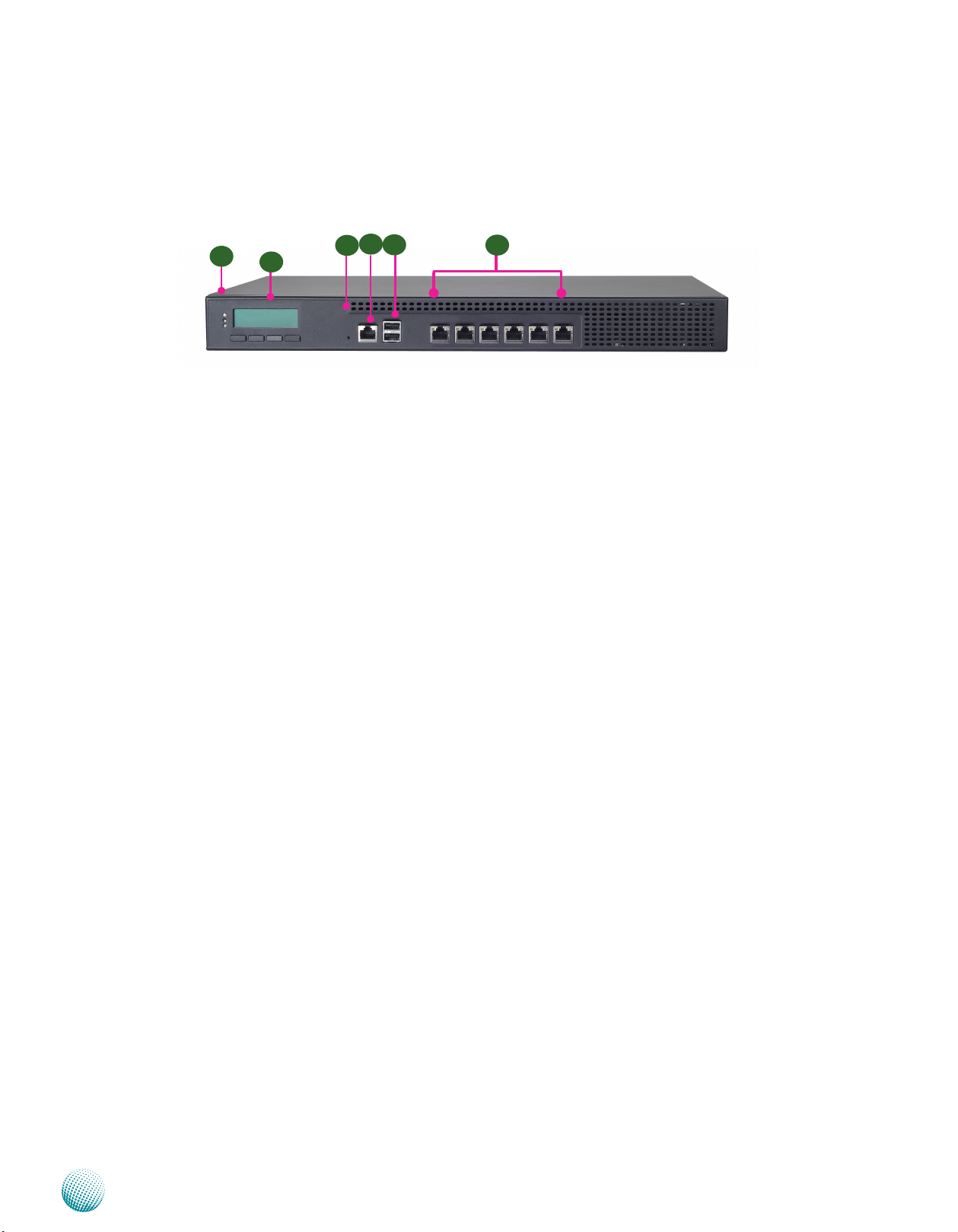
Front Panel Features
F4
F1
F2
F3
F5
LAN1
F1 Power/Status/HDD LED
Power: If the LED is on it indicates that the system is powered on. If it is off, it indicates that the system is powered off.
Status: If the LED is green, it indicates that the system’s operational state is normal. If it is red, it indicates that the system is
malfunctioning.
HDD: If the LED blinks, it indicates data access activities. Otherwise, it remains off.
F6
F2 System Panel
The LCD System Panel can be programmed to display operating status and configuration information. For more details or
sample programming code, please refer to Appendix C Programming the LCM.
F3 Reset Switch
The reset switch can be used to reboot the system without turning off the power.
F4 Console Port
By using suitable rollover cable or RJ-45 to DB-9 Female, you can connect to a computer terminal for diagnostic or
configuration purpose. Terminal Configuration Parameters: 115200 baud, 8 data bits, no parity, 1 stop bit , no flow control.
F5 Two USB 2.0 Ports
It connects to any USB devices; for example, a flash drive.
F6 6 Gigabit LAN ports (provided by Intel 82583V or 82574L for model FW-7582D)
Left LED (Yellow): If the LED is on, it indicates that the port is linked/active. If it blinks, it indicates network activity.
Right LED (Clear): If the LED is orange, it indicates that the connection speed is 1000Mbps. If the LED is green, it indicates
that the connection speed is 100Mbps. If the LED is off, the connection speed is 10Mbps.
3 pairs (LAN1-LAN2, LAN3-LAN4, LAN5-LAN6) can be configured as LAN Bypass when failure events occur. This feature is
implemented in hardware using watch dog timer functionality. Refer to Appendix D Programming Lan Bypass for a sample
implementation of this feature.
LAN1 is capable of the Preboot eXecution Environment (PXE), which allows you to boot computers using a network interface
independently of data storage devices (like hard disks) or installed operating systems. Enable this function with this option
here.
Network Application Platforms
3
Page 8
Chapter 1
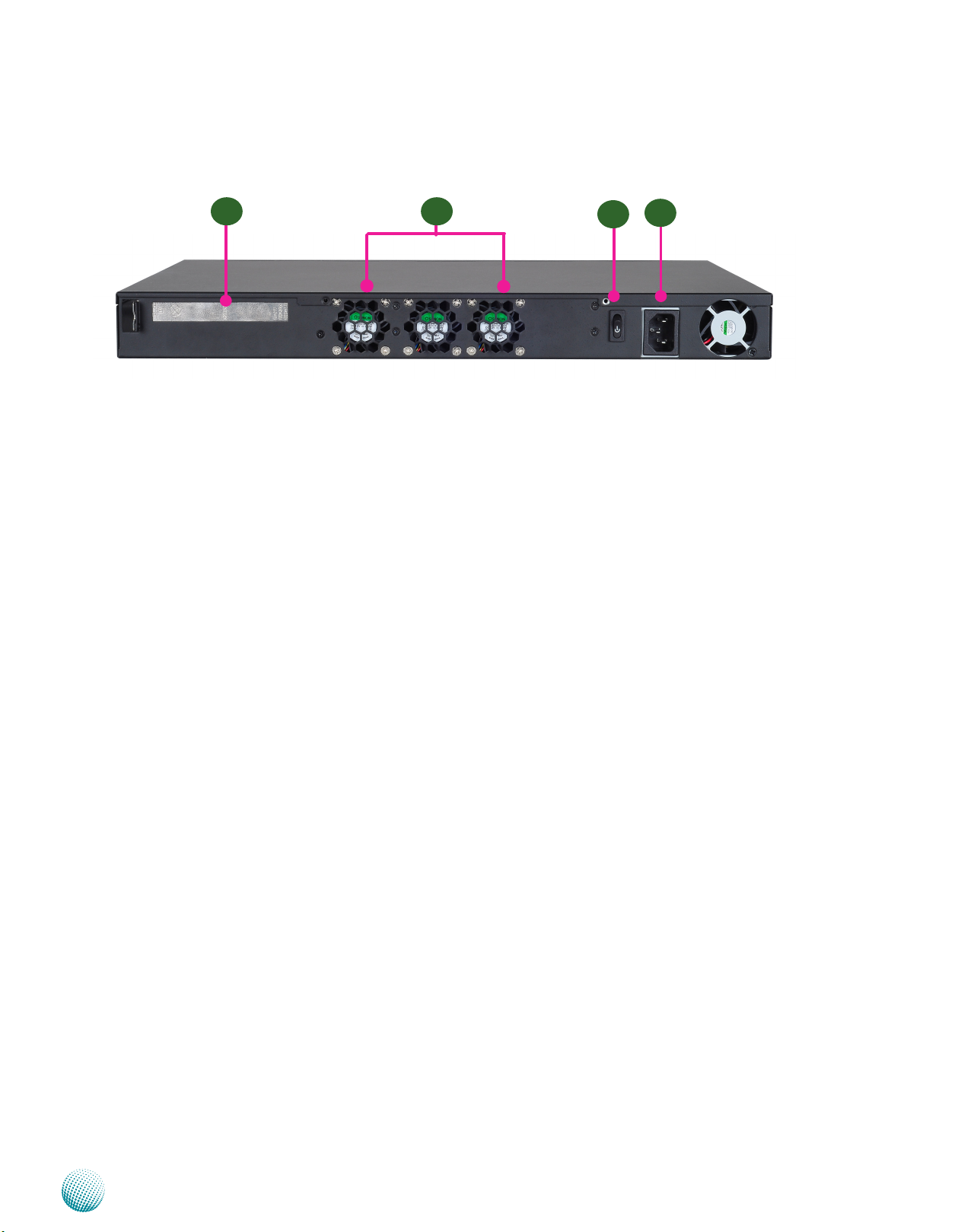
Rear Panel Features
Introduction
R1 R2
R1 Low profile Expansion slot: A slot for connecting the extended PCI-E card
The slot is for installing an additional adapter card which is connected to the main board via a riser card.
R2 System and CPU fan (from left to right: SYS fan , AUX fan, CPU FAN0)
R3 ATX Power Switch
R4 AC Power-in socket
R3
R4
Network Application Platforms
4
Page 9

Chapter 2
Introduction
Chapter 2: Hardware Setup
Preparing the Hardware Installation
To access some components and perform certain service
procedures, you must perform the following procedures
first.
WARNING: To reduce the risk of personal injury,
electric shock, or damage to the equipment,
remove the power cord to remove power from the
server. The front panel Power On/Standby button
does not completely shut off system power.
Portions of the power supply and some internal
circuitry remain active until AC power is removed.
Unpower the FW-7582 and remove the power cord.1.
Unscrew the 3 threaded screws from the top cover of 2.
the FW-7582 System.
Slide the cover backwards and open the cover 3.
upwards.
2
Note:
The motherboards can support up to 16 GB 1.
memory capacity in maximum. .
The memory has to meet with the following 2.
standard: DDR3 1066/1333MHz, Non-ECC,
Unbuffered
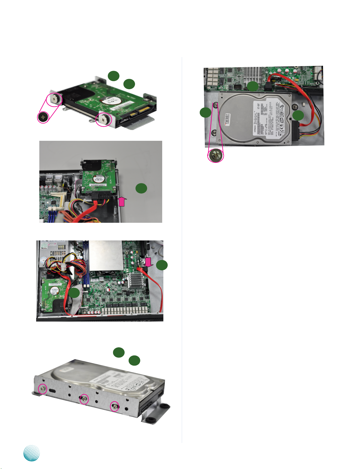
Installing the Hard Disk
The system can accommodate one Serial-ATA disks. Follow
these steps to install a hard disk into the FW-7582:
Unsrew the 4 screws on the hard disk tray to take out 1.
the hard disk tray from the system.
Place hard disk on the hard disk tray and align the holes 2.
of the hard disk with the mounting holes on the tray.
Secure the hard disk with 4 mounting screws on the 3.
hard disk tray.
Connect the Serial-ATA power and data cables to the 4.
hard disk’s power and data connectors respectively.
Fix the hard disk back to the system with the screws.5.
Plug the Serial-ATA cable to the Serial-ATA Connector 6.
on the main board.
1
Installing the System Memory
The motherboard supports DDR3 memory to meet the
higher bandwidth requirements of the latest operating
system and Internet applications. It comes with two
Double Data Rate(DDR3) Dual Inline Memory Modules
(DIMM) sockets.
Open the DIMM slot latches.1.
Install the DIMM.2.
1
2
Network Application Platforms
1
5
Page 10
Chapter 2
2.5” SATA Installation
Introduction
2
3
6
5
4
6
4
5
3.5” SATA Installation
Network Application Platforms
2
3
6
Page 11
Chapter 2
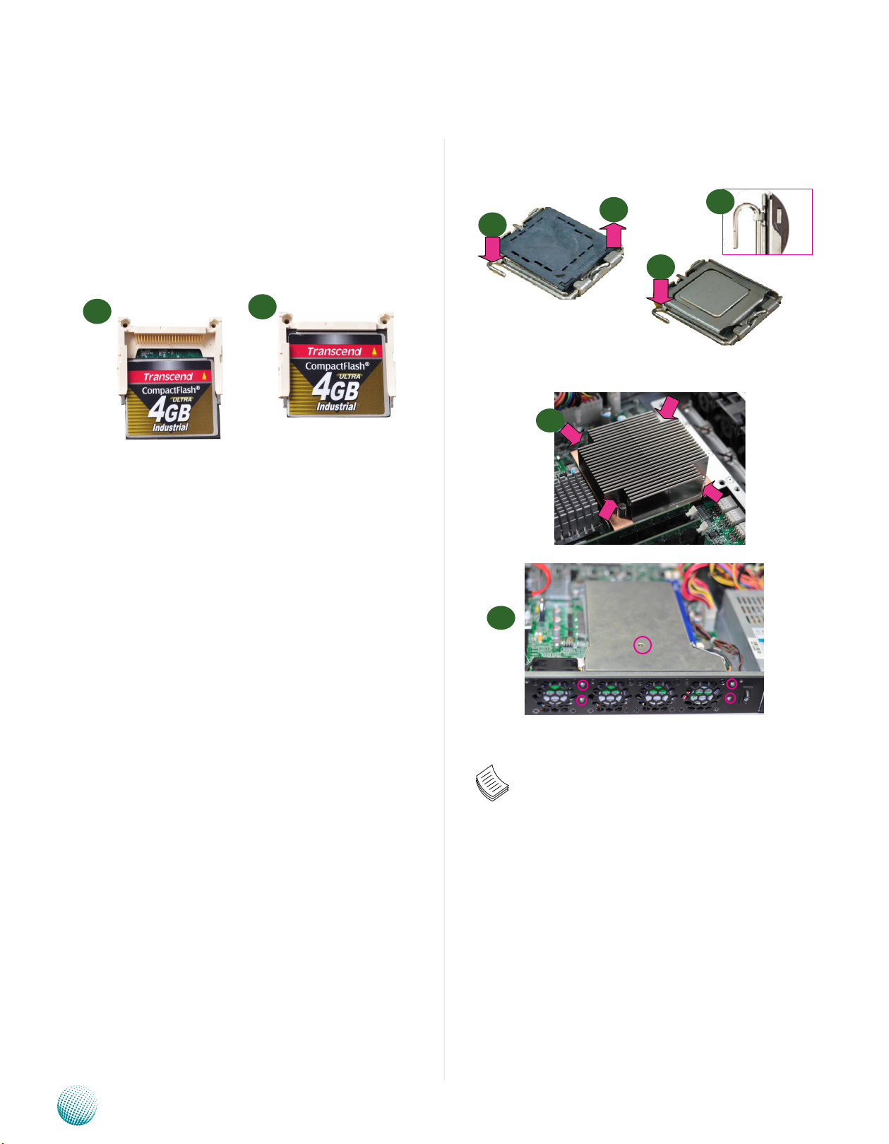
Installing a CompactFlash Card
FW-7582 provides one CompactFlash slot. Follow the
procedures bellow for installing a CompactFlash card.
Align CompactFlash card and the card slot with the 1.
arrow pointing toward the connector.
Introduction
3
2
5
Push the card to insert into the connector.2.
1
2
.
CPU and the Heat Sink Installation
The FW-7582 sever system is powered by the MB-7582
sever board, which comes with one ZIF type LGA1155 CPU
socket.
Follow the procedures bellow for installing a CPU
Remove the CPU socket cap.1.
Press the load lever and release it from the retention 2.
tab.
Lift the load lever and then the plate.3.
4
7
8
Align the cut-out of the CPU and the the notch on 4.
the socket. The CPU should fit perfectly into the
socket. Note that the CPU fits in the socket in only one
direction.
Close the plate and push the load lever to lock it back 5.
to the retention tab.
Peel off the sticker on the CPU to expose the thermal 6.
compound.
Put the heatsink on the installed CPU, match the 7.
screws with the screw holes on the board. Fasten two
screws which are opposite to each other at a time and
then the other two. It is easier this way because of the
springiness of the bracket.
Place the heatsink cover on top of the installed heatsink 8.
and screw 5 screws to fasten it on the chassis.
Note:
The CPU heat sink could only be installed in only 1.
one direction as shown in the picture.
To protect the CPU socket pins, retain the CPU 2.
cap when the CPU is not installed.
Network Application Platforms
7
Page 12

Chapter 2
Sandy Bridge H2
(LGA 1155)
INTEL
H61
LPC
6x GbE RJ-45
Connector s w/ LED
6x PCI -E x1
DDR3 MHz
Non-ECC Unbuffered
2x 2.5" or
1x 3.5"
HD Bay
DMI x4
Compact Fla sh
2x USB
PIN header
2x USB
connectors
USB 2.0
3x SATAII
2x SATAI I P orts
Dual
Channels
Up to 8GB Maximum
PCI-E x8 Golden Finger
Intel
82583V
Intel
82583 V
Winbond
83627DHG-P
2x Console
PIN header
LCM
KB/Mouse
GPIO
Fan Monitor
Thermal Monitor
SPI
Intel
82583V
Intel
82583V
Intel
82583V
Intel
83583 V
TPM
VGA
VGA PIN Header
For REAR DB19
RJ45
console
Watch dog
Reset
Bottom
By-pass
MB-8758
FDI
By-passBy-pass
Chapter 2: Motherboard Information
Block Diagram
The block diagram depicts the relationships among the
interfaces or modules on the motherboard. Please refer
to the following figure for your motherboard’s layout
design.
Up to 16GB Maximum
Motherboard Information
Network Application Platforms
MB-7582
8
Page 13
Chapter 2
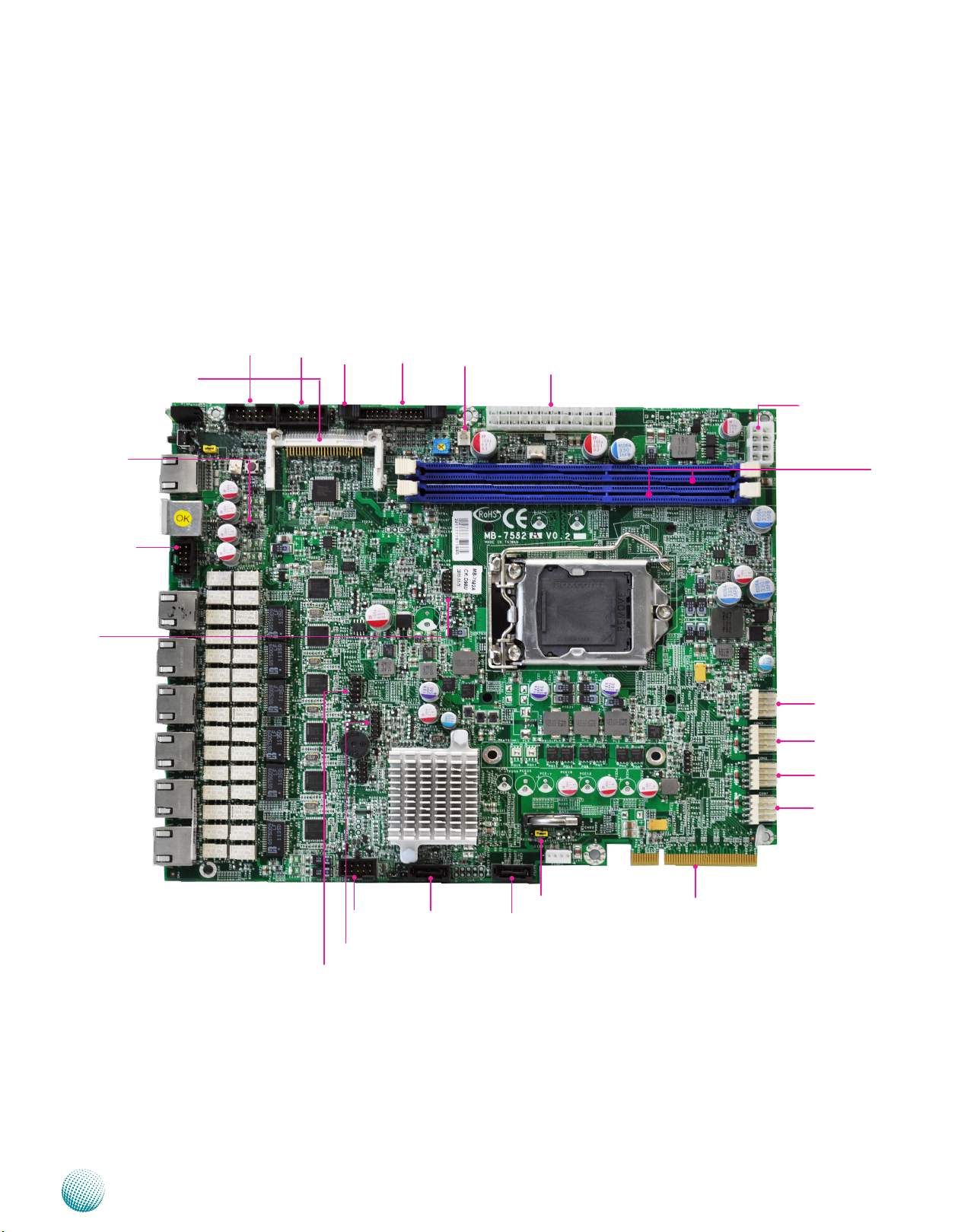
Motherboard Layout
The motherboard layout shows the connectors and
jumpers on the board. Refer to the following picture
as a reference of the pin assignments and the internal
connectors.
Motherboard Information
CF Card Connector (CF1)
J21
USB Cable
Connector
(USBA1)
LPC1
COMB2
COMB3
J10
J14
J18
ATX1
M16
ATX2
J3/J4
CON4
CON3
CON2
Network Application Platforms
USBA2
VGAA1
SPI ROM Update Jumper
(SPI-ROM1)
SATA 1
SATA 2
CMOS
CON1
PCIe Gold Finger
9
Page 14

Chapter 2
25 1
50 26
CF1
Motherboard Information
Jumper Settings
VGA Interface (VGAA1): An 2x6 (2.0mm) header for
connecting the VGA interface cable. The VGA is provided
by Intel® Graphic Media Accelerator 3150:
11
12
10
Pin No. Pin Name Pin No. Pin Name
1 Red 2 GND
3 Green 4 GND
5 Blue 6 GND
7 HSYNC 8 NC
9 VSYNC 10 GND
11 Detect-display Data 12 Deteck-display CLOCK
9
7
8
5
6
3
4
1
2
AT/ATX Mode Selection Jumper(J21): This jumper is used
for switching power mode between AT and ATX. Please
adjust them accordingly as described in the following
jumper settings.
Pin No. Function
1 2
-- ATX mode (Default)
1-2 AT mode
4 Pin TACT Power Button for debug purpose (SW1):
1
3
2
4
Pin No. Function
1 Ground
2 Ground
3 PWR_BTN_N
4 PWR_BTN_N
2-pin System Power Switch (CONN2): This connector is
for connecting power switch in ATX mode .
Pin No. Pin name
1 PWR_BTN_N
2 1
2 GND
CompactFlash Connector (CF1): It is for connecting a
Compact Flash card to be served as your system’s storage.
USB Connector (USBA1/USBA2) : An 2x5 pin header for
connecting the USB module cable. It complies with USB2.0
and support up to 480 Mbps connection speed.
Pin No. Pin Name Pin No. Pin Name
AT Mode Power Button Connector (J18): It is for
connecting power switch in AT mode. Note that you will
need to adjust the AT/ATX mode selection jumper J21.
Network Application Platforms
2 4 6 8 10
1 3 5 7 9
USBA2
1 VCC 2 VCC
3 USBD- 4 USBD5 USBD+ 6 USBD+
7 GND 8 GND
9 GND 10 GND
Pin No. Function
1 PSON#
1 2
2 Ground
1
3
5
7
9
USBA1
10
PIN DESCRIPTION PIN DESCRIPTION
1 GND 26 CF_DIS_N
2 DATA3 27 DATA11
2
4
6
8
3 DATA4 28 DATA12
4 DATA5 29 DATA13
5 DATA6 30 DATA14
6 DATA7 31 DATA15
7 -CF_DCS0 32 -CF_DCS1
8 GND 33 CF_VS1
9 GND 34 IOR#
10 GND 35 IOW#
11 GND 36 +3.3V
12 GND 37 CF_IDEIRQ
13 +3.3V 38 +3.3V
14 GND 39 MST_SLV
15 GND 40 CF_VS2
16 GND 41 CF_IDERST_N
17 GND 42 CF_IORDY
18 A2 43 CF_DMARQ
19 A1 44 CF_DDACK_N
20 A0 45 CFACT_N
21 DATA0 46 CF_PDIAG
22 DATA1 47 DATA8
23 DATA2 48 DATA9
24 NC 49 DATA10
25 CF_DIS_N 50 GND
10
Page 15

Chapter 2
Motherboard Information
Power Debug Port(psvid_p1)
1
2
3
4
Pin No. Function
1 H_VIDALERT_VR
2 H_VIDSOUT_VR
3 H_VIDSCK_VR
4 GND
Selection between PCI-E Reset and System Reset (J16):
A 1x3 (2.54mm) pin header for PCI-E reset and system
reset function.
Pin No. Function
3 2 1
1-2 SYSTEM RESET
2-3 PCI-E Reset (Default)
Front LCD Module Connector(J14): A 2x5 (2.00mm) pin
header for connecting the front system LCD display.
23 21 19 17 15 13 11 9 7 5 3 1
24 22020 18 16 14 12 10 8 6 4 2
Pin No. Function PIN NO. DESCRIPTION
1 +5V 2 Ground
3 LSLIN# 4 VEE
5 LAFD# 6 LINIT#
7 FL_PD1 8 FL_PD0
9 FL_PD3 10 FL_PD2
11 FL_PD5 12 FL_PD4
13 FL_PD7 14 FL_PD6
15 LCD- 16 +5V
17 KPA1 18 KPA2
19 KPA3 20 KPA4
21 LCM_RST 22 CTR-GRN
23 CTR-YEW 24 HDDLED_N
Clear CMOS jumper (J8): It is for clearing the CMOS
memory and system setup parameters by erasing the data
stored in the CMOS RAM such as the system passwords.
Pin No. Function
3 2 1
1-2 Normal (Default)
2-3 Clear CMOS
DIMM Socket (J3, J4): The 240-pin DDR3 DIMM is for
connecting the DDR3 1066/1333 memory. The system
can support up to 16 GB in maximum and Dual-channel
architecture. Dual channel doubles data throughput
from the memory to the memory controller by maximize
memory throughput from 64-bit buses to 128-bit bus.
SATA 1 and 2 Connectors (SATA1, SATA2): It is for
connecting a 2.5’’ SATA hard disk to be served as your
system’s storage. The system can support a maximum of
2 disks. It conforms with SATA II (3.0 Gbs).
Pin No. Function
1 GND
1 2 3 4 5 6 7
2 TX_P
3 TX_M
4 GND
5 RX_M
6 RX_P
7 GND
Console Port Cconnector (COMB1)
Pin No. Function Pin No. Function
1 Request To Send
(RTSB#)
3 Transmit Data (TXDB) 4 GND
5 GND 6 Receive Data
7 Data Set Ready
(DSRB #)
2 Data Terminal
Ready (DTRB#)
(RXDB)
8 Clear To Send
(CTSB #)
Hardware or Software Reset Jumper(J13, right next to
SW2): The jumper can be adjusted to be in either hardware
or software reset mode when the reset switch is pressed.
The hardware reset will reboot the system without turning
off the power. The software reset can be programmed to
reset software to its default settings.
Pin No. Function
3 2 1
Network Application Platforms
1-2 Hardware reset
2-3 Software reset (default)
SPI-ROM Update Connector (SPI-ROM1): Using the
appropriate cable to connect this 10-pin ISP header
connector, the SPI Flash soldered on board can be
updated.
10
8
6
4
2
7
5
3
1
1 SPI_HD1_N 2 PCH_SPI_CS1_N
3 SPI_CS0 4 V_3P3_SPI
5 SPI_ICH_MISO_R 6 SPI_HOLD0_L
7 NC 8 SPI_ICH_CLK_R
9 Ground 10 SPI_ICH_MOSI_R
Pin No. Function Pin No. Function
9
LPC I/O bus (Port 80) (LPC1): A 2x5 Pin Header 2.00mm.
It is a proprietary connector for connecting a checkpoint
device to output checkpoints throughout bootblock and
Power-On Self Test (POST) to indicate the task the system
is currently executing.
11
Page 16

Chapter 2
Motherboard Information
1
2
9
10
Pin No. Function Pin No. Function
1 CLK_33M_P80
3 RST_80DGPT_N
5 LPC_FRAME_N
7 LPC_LAD3
9 LPC_LAD2
2
4
6
8
10
LPC_LAD1
LPC_LAD0
+3.3V
Ground
Ground
ATX Power Connector(ATX1, ATX2): These 24-pin and
8-pin connectors are for connecting ATX power supply
plugs. Find the proper orientation when inserting the
plugs, for the supply plugs are designed to fit these
connectors in only one orientation.
1 23
2 24
Pin No. Pin name Pin No. Pin name
1 +3.3V 2 +3.3V
3 +3.3V 4 -12V
5 Ground 6 Ground
7 +5V 8 PSON-
9 Ground 10 Ground
11 +5V 12 Ground
13 Ground 14 Ground
15 Power Good 16 NC
17 StandBy 5V 18 +5V
19 +12V 20 +5V
21 +12V 22 +5V
23 +3.3V 24 Ground
2
4
6
8
Pin No. Pin name Pin No. Pin name
1
3
5
7
1 Ground
3 Ground 4 +12V
5 Ground 6 +12V
7 Ground 8 +12V
2 +12V
CPU Fan Connectors (CON1/CON2/CON3/CON4): 4-pin
connector for connecting the fans to be monitored with
the smart fan control. Connect CPU fan 0 and 1 to CON3
and CON4 respectively; connect SYS fan to CON 1 and
connect AUX fan to CON2. See H/W monitor setting in the
BIOS menu.
1 2 3 4 5
Pin No. Function
1 SYSFANOUTPWM
2 NC
3 SYSFANIN
4 VFAN1
5 Ground
CPU Socket: The LGA 1155 socket is for connecting the
CPU.
PCIEC1: PCI Express x8 Connectors with PCIEx8 mode
Pin No. Function Pin No. Function
B1 +12V A1 PRSNT1#
B2 +12V A2 +12V
B3 +12V A3 +12V
B4 GND A4 GND
B5 SMCLK A5 JTAG2
B6 SMDAT A6 JTAG3
B7 GND A7 JTAG4
B8 +3.3V A8 JTAG5
B9 JTAG1 A9 +3.3V
B10 3.3VAUX A10 +3.3V
B11 WAKE# A11 PERST#
B12 BYPASS0 Mode A12 GND
B13 GND A13 REFCLKA+
B14 CPUPETP0 A14 REFCLKAB15 CPUPETN0 A15 GND
B16 GND A16 CPUPERP0
B17 LANM0_LATCH_H A17 CPUPERN0
B18 GND A18 GND
B19 CPUPETP1 A19 BYPASS1 Mode
B20 CPUPETN1 A20 GND
B21 GND A21 CPUPERP1
B22 GND A22 CPUPERN1
B23 CPUPETP2 A23 GND
B24 CPUPETN2 A24 GND
B25 GND A25 CPUPERP2
B26 GND A26 CPUPERN2
B27 CPUPETP3 A27 GND
B28 CPUPETN3 A28 GND
B29 GND A29 CPUPERP3
B30 REFCLK1A+ A30 CPUPERN3
B31 REFCLK1A- A31 GND
B32 GND A32 LANM1_LATCH_H
B33 CPUPETP4 A33 LANM1_LATCH_L
B34 CPUPETH4 A34 GND
B35 GND A35 CPUPERP4
B36 GND A36 CPUPERN4
B37 CPUPETP5 A37 GND
B38 CPUPETN5 A38 GND
B39 GND A39 CPUPERP5
B40 GND A40 CPUPERN5
B41 CPUPETP6 A41 GND
B42 CPUPETN6 A42 GND
B43 GND A43 CPUPERP6
B44 GND A44 CPUPERN6
B45 CPUPETP7 A45 GND
B46 CPUPETN7 A46 GND
B47 GND A47 CPUPERP7
B48 LANM0_LATCH_L A48 CPUPERN7
B49 GND A49 GND
Network Application Platforms
12
Page 17

Chapter 2
Serial Port #1 Connector (COMB2)
Pin No. Function
1 Data Carrier Detect (DCDB#)
2 Data Set Ready (DSRB#)
9 1
10 2
Generation 3 bypass firmware programming connector
(COMB3)
9 1
10 2
3 Receive Data (RXDB)
4 Request To Send (RTSB#)
5 Transmit Data (TXDB)
6 Clear To Send (CTSB#)
7 Data Terminal Ready (DTRB#)
8 Ring Indicator (RIB #)
9 Ground
10 KEY
Pin No. Function
1
2
3
4
Request To Send (RTSB#)
5 Transmit Data (TXDB)
6 Clear To Send (CTSB#)
7 NC
8 NC
9 Ground
10 P3V3_SB
NC
NC
Receive Data (RXDB)
Motherboard Information
Case Open Signal Connector (CONN1): Connecting this
for detecting case open event
Pin No. Function
1 2 3
1
2
3
GND
CASE OPEN
GND
SATA Power Connector (PS4P1)
Pin No. Function
4 3 2 1
1
2
3
4 P5V
P12V
GND
GND
Network Application Platforms
13
Page 18

Chapter 4
Chapter 4: BIOS Settings
Updating the BIOS
The Basic Input/Output System (BIOS) can be updated
using the designated Flash Utility. To obtain the utility,
please contact us either through the sales rep or technical
support.
Note:
For the update version of the BIOS image, please
visit Lanner’s support page at
http://assist.lannerinc.com. Then select support
center from the Main Menu and look under the
folder for the desired product category. The
resources for each product including the BIOS
image will be contained within a folder named by
the product model.
Bios Settings
Network Application Platforms
14
Page 19

Chapter 4
Accessing the BIOS menu
When you are installing a motherboard or when the
system prompts “Run Setup” during start-up, you will use
the BIOS Setup program to configure the system, . This
section explains how to configure your system using this
program.
Even if you are not prompted to enter the BIOS Setup
program when you are installing a motherboard, you can
still change the configuration of your computer later on
with this program. For example, you may want to enable
the security password feature or change the power
management settings. This requires you to reconfigure
your system by using the BIOS Setup program so that the
computer can recognize these changes and record them
in the CMOS RAM .
When you start up the computer, the system provides you
with the opportunity to run this program. Press <Delete>
during the Power-On-Self-Test (POST) to enter the Setup
utility (There are a few cases that other keys may be
used, such as <F1>, <F2>, and so forth.); otherwise, POST
continues with its test routines.
If you wish to enter Setup after POST, restart the system
by pressing <Ctrl+Alt+Delete>, or by pressing the reset
button on the system chassis. You can also restart by
turning the system off and then back on. Do this last
option only if the first two failed.
The Setup program is designed to make it as easy to use as
possible. Being a menu-driven program, it lets you scroll
through the various sub-menus and make your selections
from the available options using the navigation keys.
Bios Settings
Keys Description
-><- Left/Right The Left and Right <Arrow> keys
->
->
Up/Down The Up and Down <Arrow> keys
+- Plus/Minuss The Plus and Minus <Arrow> keys
Tab The <Tab> key allows you to select
allow you to select an setup screen.
For example: Main screen, Advanced
screen, Boot screen, and so on.
allow you to select an setup item or
sub-screen.
allow you to change the field value
of a particular setup item. For
example: Date and Time.
setup fields.
Note: This manual describes the standard look of
the setup screen. There may be some instances in which
the motherboard features can vary from one to another
due to customization. This means that some of the options
described in this manual mays not match that of your
motherboard’s AMIBIOS.
Navigating the BIOS menu
The BIOS setup utility uses a key-based navigation system
called hot keys. Most of the BIOS setup utility hot keys can
be used at any time during the setup navigation process.
These keys include <F1>, <F10>, <Enter>, <ESC>, <Arrow>
keys, and so on.
Network Application Platforms
Note: The <F8> key on your keyboard is the Fail-Safe key.
It is not displayed on the key legend by default. To set the
Fail-Safe settings of the BIOS, press the <F8> key on your
keyboard. The Fail-Safe settings allow the motherboard
to boot up with the least amount of options set. This can
lessen the probability of conflicting settings.
15
Page 20

Chapter 4
The Main Menu
The main BIOS setup menu is the first screen that you can
navigate. Each main BIOS setup menu option is described
in this chapter.
The Main BIOS setup menu screen has two main frames. The
left frame displays all the options that can be configured.
“Grayed-out” options are configured parameters and
cannot be modified. On the other hand, Options in blue
can be modified.
The right frame displays the key legend. Above the key
legend is an area reserved for a text message. When an
option is selected in the left frame, it is highlighted in
white. Often a text message will accompany it.
Bios Settings
System Language
Use this item to choose the BIOS language.
System Time/System Date
Use this option to change the system time and date.
Highlight System Time or System Date using the <Arrow>
keys. Enter new values through the keyboard. Press the
<Tab> key or the <Arrow> keys to move between fields.
The date must be entered in MM/DD/YY format. The time
is entered in HH:MM:SS format.
Network Application Platforms
16
Page 21

Chapter 4
Advanced Settings
Select the Advanced tab from the setup screen to enter
the Advanced BIOS Setup screen. You can select any of
the items in the left frame of the screen, such as SuperIO
Configuration, to go to the sub menu for that item. You
can display an Advanced BIOS
Setup option by highlighting it using the <Arrow> keys.
All Advanced BIOS Setup options are described in this
section. The Advanced BIOS Setup screen is shown at
the right. The sub menus are described on the following
pages.
Bios Settings
LAN PXE Boot
The Preboot eXecution Environment (PXE) allows you to
boot computers using a network interface independently
of data storage devices (like hard disks) or installed
operating systems. Enable or disable this function on
LAN1 with this option here.
Restore on AC Power Loss
This option lets you set the state of the system when it has
just recovered from a power outage.
Option Description
Power O When setting to Power O, the system goes
into “o state” after an AC power interruption.
Power On When setting to Power on, the system turns
on automatically after a power interruption
Last State When setting to Last State, the system goes
into whatever the state was before the
power interruption.
Network Application Platforms
17
Page 22

Chapter 4
CPU Configuration Settings
You can use this screen to view the capabilities and of your
CPU. You can also use this menu to enable/disable certain
functions of your CPU. Use the up and down <Arrow> keys
to select an item. Use the <Plus> and <Minus> keys to
change the value of the selected option. A description of
the selected item appears on the right side of the screen.
The settings are described below.
Item Selection
Active Processor Core
Limit CPUID
Maximum
Execute Disable Bit
Intel Virtualization
Select the number of processor cores to
be active.
Allows legacy operating systems to boot
even without support CPUs with extended CPUID functions.
Select to enable or disable this function
Select to enable or disable the No-Execution Page Protection Technology.
The Intel VT is a hardware-assisted virtualization. This processor supports Intel Virtualization. Enable or disable this feature.
Bios Settings
SATA Controllers Configuration Settings
While entering Setup, the BIOS automatically detects
the presence of SATA devices. The SATA Port items show
“Empty” if no SATA device is installed to the corresponding
SATA port.
SATA Controllers
Item Selection
Enable or
Disable SATA
Controller(s)
Set this value to enable or disable SATA
controllers
Network Application Platforms
18
Page 23

Chapter 4
SATA Mode Selection
The system supports advanced SATA features such as
software RAID.
Item Selection
IDE Mode Set to IDE mode when your want to use the
Serial-ATA hard disk drives as Parallel ATA physical
storage devices.
AHCI Mode Set to AHCI mode when you want the SATA
hard disk drives to use the AHCI (Advanced
Host Controller Interface). The AHCI allows the
onboard storage driver to enable advanced SATA
features that increases storage performance or
workloads where multiple simultaneous read/
write requests are outstanding, most often
occurring in server-type applications (native
command queuing). It also facilitates hot
swapping.
Bios Settings
Network Application Platforms
19
Page 24

Chapter 4
USB Configuration Setting
You can use this screen to select options for the USB
Configuration. Use the up and down <Arrow> keys to
select an item. Use the <Plus> and <Minus> keys to
change the value of the selected option. The settings are
described on the following pages.
Legacy USB Support
This option enable or disable the support for USB devices
on legacy operating systems (OS), e.g., Windows ME/98/
NT, and MS-DOS. Normally if this option is not enabled,
any attached USB mouse or USB keyboard will not become
available until a USB compatible operating system is fully
booted with all USB drivers loaded. When this option is
enabled, any attached USB mouse or USB keyboard can
be used on the system even when there is no USB drivers
loaded on it.
Bios Settings
Option Description
Auto Allow the system to detect the presence of USB
devices at startup. If detected, the USB controller
legacy mode is enabled If it is not detected, the
USB control er legacy mode is disabled.
Enabled Enable the support for USB devices on legacy
operating system
Disabled Disable this function.
EHCI Hand-Off
It allows you to enable support for operating systems which do
not have the Enhanced Host Controller Interface hand-off (EHCI
hand-off ) feature for USB devices.
Option Description
Enabled Enable this feature
Disabled Disable this feature
Network Application Platforms
20
Page 25

Chapter 4
USB Hardware Delays a
The menu sets delay time for USB operations.
Item Description
USB transfer
time-out
Device reset
time-out
Device
power-up
delay
set transfers to an endpoint to complete
within a specic time.
•Ifsettozero,transferswillnottimeout
because the host controller will not cancel
the transfer. In this case, the transfer waits
indenitely until it is manually canceled or
the transfer completes normally.
•Ifsettoanonzerovalue(time-outinterval), the host controller starts a timer when
it receives the transfer request. When the
timer exceeds the set time-out interval, the
request is canceled.
This option sets the reset timing for the
USB Mass Storage to be initialized.
When set to 10 Sec, the BIOS will wait for
up to 30 seconds for the USB ash drive to
initialize.
This option sets the power-up timing for
the USB Mass Storage to be initialized.
Bios Settings
Super IO Configuration
The SuperIO configuration lets you view the IRQ address
of the serial ports of the system. You can also enable or
disable the serial communication ports here.
Network Application Platforms
21
Page 26

Chapter 4
SuperIO Configuration
In this screen, you will be able to modify the IRQ address
of the serial and parallel ports which are provided by the
Winbond W83627DHG chip.
Serial Port 0/1 Configuration
This option specifies the base I/O port address and
Interrupt Request address of serial port 0 and 1.
Bios Settings
item Selection
Enabled/
Disabled
Change
Settings
Set this value to prevent the serial port from
accessing any system resources. When this
option is set to Disabled, the serial port physically
becomes unavailable.
Selects the serial port base address and IRQ for
the interrupt address.
Parallel Port Configuration
This option specifies the I/O address used by the parallel
port.
Item Selection
Parallel Port Enable or disable this parallel port
Device
Settings
Selects the serial port base address
Network Application Platforms
22
Page 27

Chapter 4
Hardware Monitor Setting
This menu shows the hardware monitor configuration
settings. Select an item then press <Enter> to display the
configuration options.
System/CPU Temperature
The onboard hardware monitor automatically detects and
displays the CPU and motherboard temperatures.
SYS/CPU/AUX FanSpeed
The onboard hardware monitor automatically detects
and displays the CPU , chassis and system fan speeds in
rotations per minute (RPM). If the fan is not connected to
the motherboard, it displays N/A.
CPU Voltage, 3.3V voltage, 5V voltage, 12V voltage
Bios Settings
The onboard hardware monitor automatically detects the
voltage output through the onboard voltage regulators.
Smart Fan Mode Configuration
It allows you to configure the smart fan feature. You
can manually turn on the CPU fan or set the target CPU
temperature at which the CPU fan will start running if the
fan is not yet turned on. And the CPU fan can also be turned
off automatically if the temperature for the CPU is at or
below the specified value. Refer to Motherboard Layout on
Chapter 3 Block Diagram for CPU fan connectors.
Item Selection
Manual
Mode
Smart Fan
Mode
Manually set the fan speed. Valid values are
from 0 to 255(full duty cycle)
This mode allows users to set target system
temperature (3 levels) at which the fan will
be running at a congured duty cycle:
CPUFAN Target T1/T2/T3: enter the temperature in 0C
CPUFAN PWM: enter the proportion of duty
cycle from 0 to 255 (full duty cycle).
Network Application Platforms
23
Page 28

Chapter 4
Serial Port Console Redirection
Use this menu to set the settings for BIOS remote access
feature.
Item Selection
Console Redirection Enable or disable BIOS
through remote access
Console Redirection Settings
COM0/COM1 Console Redirection Settings
Item Selection
Terminal Type Sets the connection termi-
Bits per second, Data bits,
Parity, Stop Bits, Flow
Control
Enter to view more options
nal type
Sets the terminal connec-
tion parameters such as
the baud rate, parity check
mechanism, etc.
Bios Settings
Network Application Platforms
24
Page 29

Chapter 4
Lan Bypass Function
In this screen, you can configure the Lan Bypass
functionality. The system have 8 LAN ports but only Lan3/4
and Lan5/6 have bypass function. (when facing the front
panel and counting from the left).
Riser Card (or Power on/Runtime) Bypass Control
You can activate or deactivate the Lan Bypass ports. For
the description of the physical ports that are capable of
the LAN Bypass function, refer to the Front Panel Feature in
Chapter 1 Introduction.
SYSOff Bypass Control
You can enable or disable the automatic activation of
hardware Lan Bypass function in the event of a power
failure. Hardware Bypass can automatically activate to
allow network traffic to continue.
Bios Settings
The Lan bypass can be turned on or off in two system
states, i.e., power on and power off. The following are the
illustration of the possibilities of LAN bypass configuration
in each state.
Bypass settings
System Status
Power on Enabled Disabled Enabled
Power o Bypass Bypass
Bypass settings
System Status
LAN Bypass for Port1 and
Port 2
Bypass Non-Bypass
LAN Bypass for Port1 and
Port 2
LAN Bypass 1&2 when
power o
LAN Bypass 1&2 when
power o
Power on Enabled Disabled Disabled
Non-Bypass Non-Bypass
Power o Non-Bypass Non-Bypass
Network Application Platforms
25
Page 30

Chapter 4
Sandy Bridge CPU PPM Configuration
In this section, you can configure the CPU Processor Power
Management.
EIST (Enhanced Intel SpeedStep Technology)
It allows you to enable or disable the EIST.
Option Description
Enable The operating system
controls the CPU speed
Disabled The CPU runs at its de-
fault speed.
Bios Settings
Enhanced Intel SpeedStep® technology (EIST) allows the
system to dynamically adjust processor voltage and core
frequency, which can result in decreased average power
consumption and decreased average heat production.
There are some system requirements must be met,
including CPU, chipset, motherboard, BIOS and operation
system. Please refer to Intel website for more information
Network Application Platforms
26
Page 31

Chapter 4
Chipset
The chipset menu will let you further configure your Intel
CPU and PCH capabilities:
PCH I/O Configuration
It shows the model name and version of the Intel Platform
Controller Hub on the system.
Bios Settings
USB Configuration
Enter to enable or disable USB EHCI (USB2.0) host
controllers.
SLP_S4 Assertion Width
Select the mininum assertion width of the SLP_S4# signal.
This field indicates the minimum assertion width of the
SLP__S4# signal to ensure that the DRAM modules have
been safely power-cycled. SLP_S4# is a signal for power
plane control. This signal shuts off power to all non-critical
systems when in the S4 (Suspend to Disk) or S5 (Soft Off )
state.
Network Application Platforms
27
Page 32

Chapter 4
System Agent (SA) Configuration
Intel VT-d
Select to enable or disable the Intel Virtualization
Technology for Directed I/O” (VT-d). The Memory and
I/O virtualization are supported by the chipset as part
of Intel Virtualization Techonology for hardware-assisted
virtualization.
Bios Settings
Memory Configuration
It shows the memory capacity of the system and the
installed memory on the system.
Network Application Platforms
28
Page 33

Chapter 4
Boot Setup
Select the Boot tab from the setup screen to enter the Boot
BIOS Setup screen. You can select any of the items in the
left frame of the screen, such as Boot Device Priority, to
go to the sub menu for that item. You can display an Boot
BIOS Setup option by highlighting it using the <Arrow>
keys. Select an item on the Boot Setup screen to access
the sub menus for the following described functions.
Boot Settings Configuration
In this screen, you will be able to configure the boot
procedures and the related elements.
Bios Settings
Items Options
Setup Prompt Timeout Specify the number of seconds
for the boot setup prompt to
wait for user’s intervention
during the POST.
Bootup Num-Lock State
Quiet Boot
GateA20 Active
This option lets you to
enable or disable the
function of the NumLock
key.
Enabling this item allows
the BIOS to suppress the
message displayed during
the POST.
This option sets the A20
address line controlling
method for handling above
1MB memory access. By
enabling the A20 gate, we
have access to all 32 lines on
the address bus, and hence,
can refrence 32 bit addresses,
or up to 0xFFFFFFFF - 4 GB
of memory. The controlling
mode includes:
Upon Request: when it is
enabled by user programs.
ALWAYS: never disables the
A20 line
Network Application Platforms
29
Page 34

Chapter 4
Items Options
Option ROM Messages
Interrupt 19 Trap Response
Boot Option Priorities
Hard Drive BBS Priorities
This option controls the
display of ROM messages
form the BIOS of add-
on devices such as the
graphics card or the SATA
controller during the start-
up sequence.
Force BIOS: When setting to
Force BIOS, third-party ROM
messages will be forced to
display during the start-up
sequence.
Keep Current: When setting to
Keep Current, third-party ROM
messages will only be displayed
if the device’s manufacturer has
set the add-on device to do so.
Set this value to configure
how option ROMs such as
network controllers trap
BIOS interrupt 19.
Use this screen to specify the
order in which the system
checks for the device to
boot from.
You will enter a submenu
that presents all the drives
connected to the system.
Here you can define the
boot order for the Hard
disks.
Bios Settings
Network Application Platforms
30
Page 35

Chapter 4
Security Settings
Select Security Setup from the Setup main BIOS setup
menu. All Security Setup options, such as password
protection and virus protection, are described in this
section. To access the sub menu for the following items,
select the item and press <Enter>:
Administrator Password
If you have set an administrator password, you should
enter the administrator password for accessing the system.
Otherwise, you will only be able to see or change selected
fields in the BIOS setup program.
Bios Settings
User Password
If you have set a user password, you must enter the user
password for accessing the system.
To set an Administrator/User password:
Select the option item and press Enter.1.
From the Create New Password box, key in a password, 2.
then press enter.
Confirm the password when prompted.3.
To change an administrator password:
Select the option item and press Enter.1.
From the Enter Current Password box, key in the 2.
current password, then press enter.
From the Create New Password box, key in a new 3.
password, then press Enter.
Confirm the password when prompted.4.
To clear the administrator password, follow the same steps
as in changing an administrator password, then press
Enter when prompted to create/confirm the password.
Network Application Platforms
31
Page 36

Chapter 4
Save & Exit
Select the Exit tab from the setup screen to enter the Exit
BIOS Setup screen. You can display an Exit BIOS Setup
option by highlighting it using the <Arrow> keys. The
following table lists the options in this menu.
Item Options
Saving Changes and Exit Select this option to save
changes and exit the BIOS
menu. It will automatically
resets if the changes made
require rebooting the
system to take effect.
Discard Changes and Exit Select this option to discard
changes and exit and BIOS
menu to continue the
booting process.
Save Changes and Reset When you have completed
the system configuration
changes, select this option
to leave setup and reboot
the computer so the new
system configuration
parameters can take effect.
Discard Changes and Reset This option allows you
to discard the selections
you made and restore the
previously saved values.
After selecting this option,
a confirmation appears.
Select Yes to discard any
changes and load the
previously saved values.
Save Changes Save your changes
Discard Changes Discard changes
Restore Defaults Restore to factory defaults
Save as User Defaults Save all of your changes as
an user default setting.
Restore User Defaults Loads your saved user
default setting.
Boot Override This section of the Boot
Menu allows booting from a
specific device immediately.
Therefore you should see
an entry for all bootable
devices.
Launch EFI Shell from
filesystem device
This option allows you to
attempt to launch the EFI
Shell application (shellx64.
e) from one of the avail-
able lesystem devices.
Bios Settings
Network Application Platforms
32
Page 37

Appendix A
Appendix A: Programming Watchdog Timer
A watchdog timer is a piece of hardware that can be
used to automatically detect system anomalies and reset
the processor in case there are any problems. Generally
speaking, a watchdog timer is based on a counter that
counts down from an initial value to zero. The software
selects the counter’s initial value and periodically restarts
it. Should the counter reach zero before the software
restarts it, the software is presumed to be malfunctioning
and the processor’s reset signal is asserted. Thus, the
processor will be restarted as if a human operator had
cycled the power.
For sample watchdog code, see watchdog folder on the
Driver and Manual CD
Programming Watchdog Timer
For sample watchdog code, see watchdog folder on the
Driver and Manual CD.
Network Application Platforms
33
Page 38

Appendix B
Appendix B: Setting up Console Redirections
Console redirection lets you monitor and configure a
system from a remote terminal computer by re-directing
keyboard input and text output through the serial port.
This following steps illustrate how to use this feature.
Connect one end of the console cable to console port 1.
of the system and the other end to serial port of the
Remote Client System.
Configure the following settings in the BIOS Setup 2.
menu
BIOS > Advanced > Remote Access Configuration >
Serial Port Mode > [115200, 8 , n ,1 ]
Setting up Console Redirection
Configure Console Redirection on the client system. 3.
The following illustration is an example on Windows
platform:
Click the start button, point to Programs > a.
Accessories > Communications and select Hyper
Terminal.
Enter any name for the new connection and select b.
any icon.
Click OK.c.
From the “Connect to”. Pull-down menu, select the d.
appropriate Com port on the client system and
click OK.
Select 115200 for the Baud Rate, None. for Flow e.
contorl, 8 for the Data Bit, None for Parity Check,
and 1 for the Stop Bit.
Network Application Platforms
34
Page 39

Appendix C
Programming the LCM
Appendix C: Programming the LCM
The LCD panel module (LCM) is designed to provide realtime operating status and configuration information for
the system. For sample LCM code, see LCM foler in the
Driver and Manual CD. The driver and the program library
can also be found in the folder.
The system support Parallel Text-based LCM. The LCM
connects to the motherboard’s parallel port. The LCD
screen can display 2 lines, 20 characters per line.
Build
To build program source code on Linux platform, use the
following steps as a guideline:
Copy the proper makefile from the Driver and Manual 1.
CD to your system: Makefile.linux
Type make to build source code:2.
make Makefile (Note: omit the file extensions)
After compiled, the executable programs (plcm_test,
plcm_cursor_char, Test) and the driver (plcm_drv.ko or
plcm_drv.o) will appear in the program’s folder.
Move Cursor right (select to move the cursor to the
right)
Move Cursor Left (select to move the cursor to the left)
Add a char (select to display a character on the LCM
screen)
Clear (select to clear the LCM display)
Leave (select to leave the program)
To execute, type:
#./ plcm_cursor_char
Note: For descriptions of the command, refer to
the Readme file contained within the program’s
folder.
Note: The OS supported by Lanner Bypass
function include platforms based on Linux Kernel
series 2.4.x and Linux Kernel series 2.6.x.
Install
Install the driver and create a node in the /dev directory
by:
#insmod plcm_drv.ko
#mknod /dev/plcm_drv c 241 0
Note: If you cannot install the driver, check
whether you have enabled the parallel port in the
BIOS setting .
Execution
This section contains sample executable programs that
you could test on your platform. It demonstrates some
useful functionality that the LCM provides.
To execute, type:
#./plcm_test
Plcm_cursor_char. This program provides a menu to
demonstrate the following functions:
Insert line (set the starting line to either line 1 or line 2)
Network Application Platforms
35
Page 40

Appendix D
Programming LAN Bypass
Appendix D: Programming LAN Bypass
The bypass function is used to link two independent
Ethernet ports when the system fails or powers off. This
means if your system is equipped with a LAN Bypass
function, a system failure or power-off event will not
interrupt your network traffic. There are typically two
statuses for the bypass, one is “Normal” state and the
other is “Bypass” status. Lanner Generation 3 bypass
utility provides software for controlling the LAN Bypass
function:
Lanner ‘s Bypass Modules include WDT (Watch Dog Timer)
controller and Bypass switch.
Our Bypass Modules also include a software development
kit that enables system designer to efficiently design
systems to support bypass functionality. Lanner Bypass
Modules with watchdog control have the following
features:
Communication through SMBUS (I2C)1.
Independent bypass status control for each pair up to 2.
a total of 4 pairs
Website at http://assist.lannerinc.com. And
browse the support center and look for Lanner
LAN Bypass Module Manual under Software
Utility Manuals folder.
For a description of the physical LAN ports 2.
equipped with this function, refer to Front Panel
Features in Chapter 1 Introduction.
Lanner Bypass Modules can bypass systems Ethernet 3.
ports on a host system during three instances: Just-on
(Just-on is the brief moment when the internal power
supply turns on and booting process starts), system
off, or upon software request (during run-time).
Software programmable bypass or normal mode4.
Software programmable timer interval:5.
- JUST-ON watchdog timer, used during JUST-ON, has
timer setting of 5~1275 seconds of timer interval.
- Run-Time watchdog timer, used during run-time, has
setting of 1~255 seconds of timer interval.
Multiple Watchdog Timers:6.
-Two for run-time: It is designed to give you a more
variety of controls of the bypass on port basis. By
using dedicated watchdogs for different pairs of
bypass, you have the flexibility to manage the bypass
status for them differently.
-One for just-on: It is designed to give you the precise
control of the bypass during this phase. You can use
this timer to delay enabling the bypass in just-on
state.
Note:
For sample LAN bypass code and the Bypass 1.
Manual, see the LAN_Bypass folder on the
Driver and Manual CD or the Lanner Assist
Network Application Platforms
36
Page 41

Appendix E
Terms and Conditions
Appendix E: Terms and Conditions
Warranty Policy
All products are under warranty against defects in 1.
materials and workmanship for a period of one year
from the date of purchase.
The buyer will bear the return freight charges for 2.
goods returned for repair within the warranty period;
whereas the manufacturer will bear the after service
freight charges for goods returned to the user.
The buyer will pay for repair (for replaced components 3.
plus service time) and transportation charges (both
ways) for items after the expiration of the warranty
period.
If the RMA Service Request Form does not meet the 4.
stated requirement as listed on “RMA Service,” RMA
goods will be returned at customer’s expense.
The following conditions are excluded from this 5.
warranty:
RMA Service
Requesting a RMA#
To obtain a RMA number, simply fill out and fax the 6.
“RMA Request Form” to your supplier.
The customer is required to fill out the problem code 7.
as listed. If your problem is not among the codes listed,
please write the symptom description in the remarks
box.
Ship the defective unit(s) on freight prepaid terms. 8.
Use the original packing materials when possible.
Mark the RMA# clearly on the box. 9.
Note: Customer is responsible for shipping
damage(s) resulting from inadequate/loose
packing of the defective unit(s). All RMA# are valid
for 30 days only; RMA goods received after the
effective RMA# period will be rejected.
Improper or inadequate maintenance by the customer
Unauthorized modification, misuse, or reversed
engineering of the product Operation outside of the
environmental specifications for the product.
Embedded and Industrial Computing
37
Page 42

Appendix E
RMA Service Request Form
When requesting RMA service, please fill out the following form. Without
this form enclosed, your RMA cannot be processed.
RMA No:
Reasons to Return: Ŀ Repair(Please include failure details)
Ŀ Testing Purpose
Company: Contact Person:
Phone No. Purchased Date:
Fax No.: Applied Date:
Return Shipping Address:
Shipping by: Ŀ Air Freight Ŀ Sea Ŀ Express ___
Ŀ Others:________________
Item Model Name Serial Number Configuration
Item Problem Code Failure Status
*Problem Code:
01:D.O.A.
02: Second Time
R.M.A.
03: CMOS Data Lost
04: FDC Fail
05: HDC Fail
06: Bad Slot
07: BIOS Problem
08: Keyboard Controller Fail
09: Cache RMA Problem
10: Memory Socket Bad
11: Hang Up Software
12: Out Look Damage
13: SCSI
14: LPT Port
15: PS2
16: LAN
17: COM Port
18: Watchdog Timer
19: DIO
20: Buzzer
21: Shut Down
22: Panel Fail
23: CRT Fail
24: Others (Pls specify)
Request Party
Confirmed By Supplier
Authorized Signature / Date Authorized Signature / Date
Terms and Conditions
Embedded and Industrial Computing
38
 Loading...