

Page 1

Network
Application Platforms
Hardware platforms for next generation networking infrastructure
FW-7581
>>
User's Manual
Publication date:2011-09-22
Page 2
About
About
Overview
Icon Descriptions
The icons are used in the manual to serve as an indication
of interest topics or important messages. Below is a
description of these icons:
NOTE: This check mark indicates that
there is a note of interest and is something
that you should pay special attention to
while using the product.
Online Resources
The listed websites are links to the on-line product
information and technical support.
Resource Website
Lanner http://www.lannerinc.com
Product Resources http://assist.lannerinc.com
WARNING: This exclamation point
indicates that there is a caution or
warning and it is something that could
damage your property or product.
Acknowledgement
Intel, Pentium and Celeron are registered trademarks of
Intel Corp.
Microsoft Windows and MS-DOS are registered trademarks
of Microsoft Corp.
All other product names or trademarks are properties of
their respective owners.
Compliances
CE
This product has passed the CE test for environmental
specifications. Test conditions for passing included the
equipment being operated within an industrial enclosure.
In order to protect the product from being damaged by
ESD (Electrostatic Discharge) and EMI leakage, we strongly
recommend the use of CE-compliant industrial enclosure
products.
FCC Class A
This equipment has been tested and found to comply
with the limits for a Class A digital device, pursuant to Part
15 of the FCC Rules. These limits are designed to provide
reasonable protection against harmful interference when
the equipment is operated in a commercial environment.
This equipment generates, uses and can radiate radio
frequency energy and, if not installed and used in
accordance with the instruction manual, may cause
harmful interference to radio communications. Operation
of this equipment in a residential area is likely to cause
harmful interference in which case the user will be required
to correct the interference at his own expense.
RMA http://eRMA.lannerinc.com
Copyright and Trademarks
This document is copyrighted, © 2011. All rights are
reserved. The original manufacturer reserves the right to
make improvements to the products described in this
manual at any time without notice.
No part of this manual may be reproduced, copied,
translated or transmitted in any form or by any means
without the prior written permission of the original
manufacturer. Information provided in this manual is
intended to be accurate and reliable. However, the original
manufacturer assumes no responsibility for its use, nor for
any infringements upon the rights of third parties that
may result from such use.
Network Application Platforms
i
Page 3

TTaTTable of Contentsbeable of Contents
Chapter 1: Introduction 1
System Specication . . . . . . . . . . . . . . . . . . . . . . . . . . . . . . . . . . . . . . . . . . . 1
Package Contents . . . . . . . . . . . . . . . . . . . . . . . . . . . . . . . . . . . . . . . . . . . . . 2
Front Panel Features. . . . . . . . . . . . . . . . . . . . . . . . . . . . . . . . . . . . . . . . . . . . 3
Rear Panel Features . . . . . . . . . . . . . . . . . . . . . . . . . . . . . . . . . . . . . . . . . . . . 4
Chapter 2: Hardware Setup 5
Preparing the Hardware Installation. . . . . . . . . . . . . . . . . . . . . . . . . . . . . . . . . . 5
Installing the System Memory . . . . . . . . . . . . . . . . . . . . . . . . . . . . . . . . . . . . . 5
Installing the Hard Disk . . . . . . . . . . . . . . . . . . . . . . . . . . . . . . . . . . . . . . . . . . 5
Installing a CompactFlash Card. . . . . . . . . . . . . . . . . . . . . . . . . . . . . . . . . . . . . 6
CPU and the Heat Sink Installation. . . . . . . . . . . . . . . . . . . . . . . . . . . . . . . . . . . 6
Chapter 3: Motherboard Information 7
Block Diagram . . . . . . . . . . . . . . . . . . . . . . . . . . . . . . . . . . . . . . . . . . . . . . . 7
Motherboard Layout . . . . . . . . . . . . . . . . . . . . . . . . . . . . . . . . . . . . . . . . . . . 8
Jumper Settings . . . . . . . . . . . . . . . . . . . . . . . . . . . . . . . . . . . . . . . . . . . . . . 9
Appendix A: Driver Installation 12
LAN Adapters Driver Installation . . . . . . . . . . . . . . . . . . . . . . . . . . . . . . . . . . . .12
On the Windows OS . . . . . . . . . . . . . . . . . . . . . . . . . . . . . . . . . . . . . . . . .12
On Linux . . . . . . . . . . . . . . . . . . . . . . . . . . . . . . . . . . . . . . . . . . . . . . . .13
VGA Driver Installation . . . . . . . . . . . . . . . . . . . . . . . . . . . . . . . . . . . . . . . . . .14
On the Windows OS . . . . . . . . . . . . . . . . . . . . . . . . . . . . . . . . . . . . . . . . .14
On Linux . . . . . . . . . . . . . . . . . . . . . . . . . . . . . . . . . . . . . . . . . . . . . . . .14
Appendix B: Programming Watchdog Timer 15
Appendix C:
Appendix D:
Appendix E:
Appendix F:
Setting up Console Redirections 16
Programming LAN Bypass 17
Programming the LCM 18
Terms and Conditions 19
Warranty Policy . . . . . . . . . . . . . . . . . . . . . . . . . . . . . . . . . . . . . . . . . . . .19
RMA Service . . . . . . . . . . . . . . . . . . . . . . . . . . . . . . . . . . . . . . . . . . . . . .19
ii
Page 4

Chapter 1
Introduction
Chapter 1: Introduction
Thank you for choosing the FW-7581. The FW-7581 is a
1U network communication appliance that is designed to
meet your demand for high quality network application
platform with its high port density. The FW-7581 comes
with 1 FE and 6 Gb Ethernet ports with one pair capable
to be an abnormal state packet bypass.
Below are key features of the FW-7581:
This platform is built around the Intel G41 chipset and 1.
supports a variety of dierent Intel processors. These
include Intel® Core 2 Quad, Core 2 Duo, Pentium® D,
Celeron CPU.
Dual-channeled 240-pin DDR3 SDRAM DIMM sockets 2.
to support up to 4 GB of unbuffered, non-ECC DDR3
memory (Dual Channel utilize two 64-bit data
channels for higher data throughput.)
Low-Profile expansion for connecting 3. the PCI-E slot
using the (x)8 lane architecture to add customized
capabilities
System Specification
Features Description
Form Factor 1U Rackmount
Supports Intel Core2 Quad,
Platform
System Memory
OS Support Windows, Linux
Storage
Networking
Processor
Chipset Intel G41 + ICH7R
Technology
Max Capacity 4GB
Socket 2 x 240P DIMM
HDD Bay(s) 1 x 2.5”
Storage Interface
Ethernet Port Density
Controller
Core2 Duo, PentiumD,
Celeron Processors,
LGA775
Dual-channel DDR3 1066 /
1333 MHz
2 x Serial ATA
1 x CompactFlash
6 x RJ45 GbE onboard
1 x RJ45 FE Mng port
6 x Intel 82574L,
1 x FE 9620DM
With the Intel® Graphics Media Accelerator X4500 4.
(Intel® GMA X4500) on the G41 Express Chipset, the
VGA port (optional) has built-in support for smooth
high-definition video playback without the need for
add-in video cards or decoders.
Bypass 1 x pair LAN Bypass
I/O Interface
Expansion PCIe 1 x PCIe (x)8
Cooling
Environmental
Parameters
Miscellaneous
Physical
Dimensions
Power
Console 1 x RJ45
USB 2 x USB 2.0
Processor
System
Temperature, ambient operating / storage
Humidity (RH), ambient operating / ambient non-operating
LCD Module 2 x 20 character
Watchdog Yes
Internal RTC with Li Battery Yes
Dimensions (WxHxD) 431 x 44.4 x 305mm
Weight 5 kg (11 lbs)
Type / Watts 1U ATX SPS / 220W
Input AC 90~264V@47~63Hz
Output
1U Passive Heatsink with 2
Cooling Fans
1 x Cooling Fan with
Smart Fan
0ºC ~40ºC / -20ºC~60ºC
5 ~ 90%, non condensing /
5 ~ 95%, non condensing
+5V output: 1V min, 12V
max;
+3.3V output: 1V min,
14V max;
+12V output 1V min, 14V
max
Network Application Platforms
1
Page 5

Chapter 1
Introduction
Approvals &
Compliance
Ordering
Information
FW-7581A
FW-7581B
CE Emission, FCC Class
A, RoHS
STD with 1pairs bypass,
with Riser card
STD without bypass, without Riser card
Package Contents
Your package contains the following items:
FW-7581 Network Security Platform•
Power cable•
1 crossover Ethernet cable (1.8 meter)•
1 straight-through Ethernet cable (1.8 meter)•
1 RJ-45 console cable•
Serial-ATA power/data cable •
1 threaded-screw set•
1 name plate label•
Drivers and user’s manual CD.•
Network Application Platforms
2
Page 6
Chapter 1
Introduction
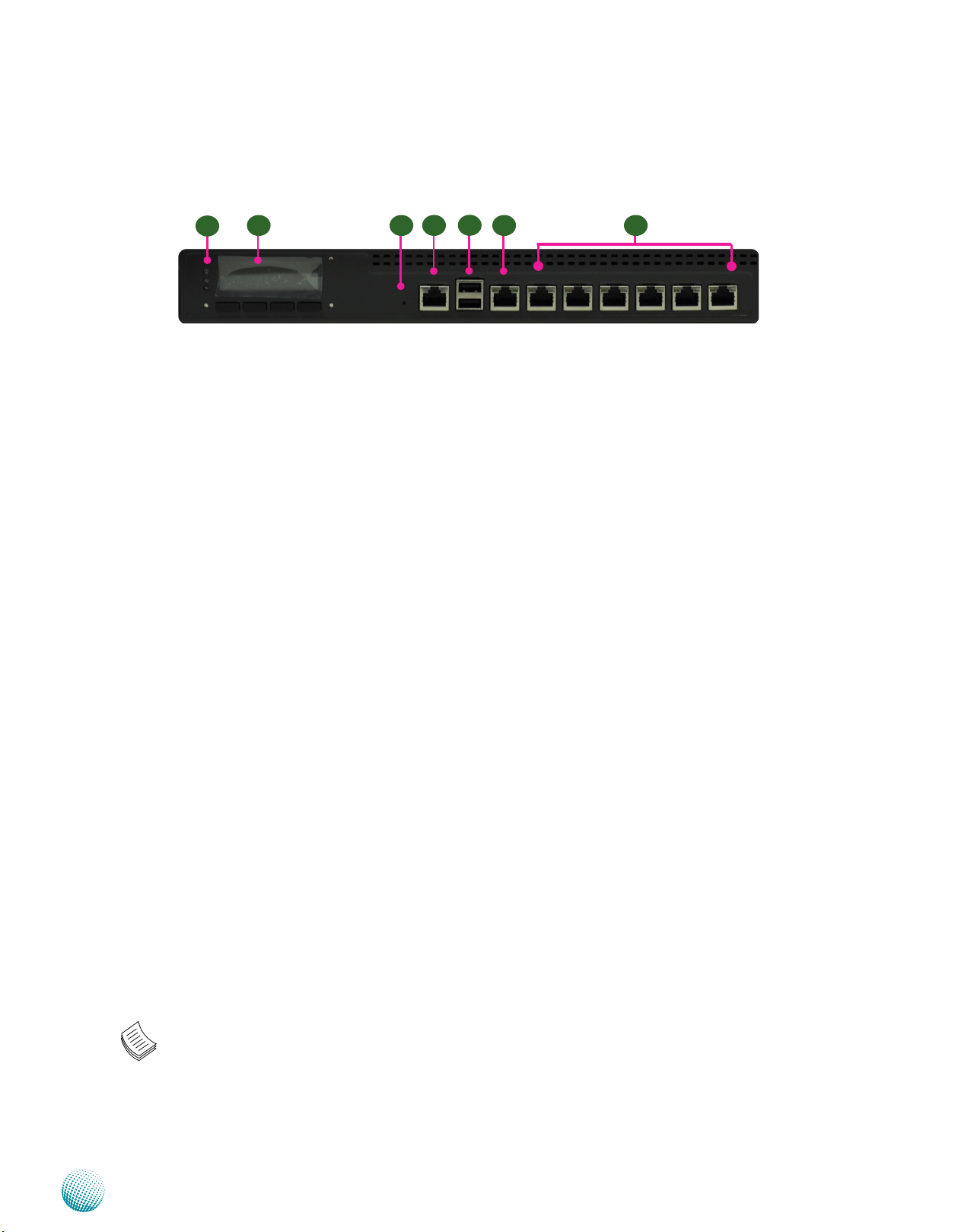
Front Panel Features
F5
F4
F1
F1 Power/Status/HDD LED
Power: If the LED is on it indicates that the system is powered on. If it is off, it indicates that the system is powered off.
Status: If the LED is green, it indicates that the system’s operational state is normal. If it is red, it indicates that the system is
malfunctioning.
HDD: If the LED is on, it indicates that the system’s storage is functional. If the LED blinks, it indicates data access activities.
If it is off, it indicates that there is no hard disk present or functional.
F2 F7F6
F3
F2 System Panel
The LCD System Panel can be programmed to display operating status and configuration information. For more details or
sample programming code, please refer to Appendix B Programming the LCM.
F3 Reset Switch
The reset switch can be used to reboot the system without turning off the power.
F4 Console Port
By using suitable rollover cable or RJ-45 to DB-9 Female, you can connect to a computer terminal for diagnostic or
configuration purpose. Terminal Configuration Parameters: 115200 baud, 8 data bits, no parity, 1 stop bit , no flow control.
F5 Two USB 2.0 Ports
It connects to any USB devices; for example, a flash drive.
F6 Management Port (provided by Intel 9620DM)
This FastEthernet port can be connected for configuration or troubleshooting purpose.
F7 6 Gigabit LAN ports (provided by Intel 82574L)
Left LED (Yellow): If the LED is on, it indicates that the port is link/active. If it blinks, it indicates network activity.
Right LED (Clear): If the LED is orange, it indicates that the connection speed is 1000Mbps. If the LED is green, it indicates
that the connection speed is 100Mbps. If the LED is off, the connection speed is 10Mbps.
1 pair (LAN5-LAN6) can be configured as LAN Bypass when failure events occur. This feature is implemented in hardware
using watch dog timer functionality. Refer to Appendix D Programming Lan Bypass for a sample implementation of this
feature.
Note:
The LAN Bypass are active only on port 5 and 6.1.
The LAN Bypass is only available on model FW-7581A.2.
Network Application Platforms
3
Page 7
Chapter 1
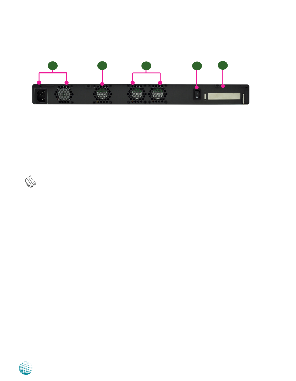
Rear Panel Features
Introduction
R1
R1 AC Power-in socket and power supply fan
R2 System Fan
R3 CPU Fan 2 and 1
R4 ATX Power Switch
R5 Low profile Expansion slot: A slot for connecting the extended PCI-E card
The slot is for installing an additional adapter card which is connected to the main board via a riser card.
Note: The system comes in with internal connectors for VGA, RS-232 serial and USB2.0 ports. These ports can be wired
to be shown on the back panel..
R2
R3
R4
R5
Network Application Platforms
4
Page 8

Chapter 2
Introduction
Chapter 2: Hardware Setup
Preparing the Hardware Installation
To access some components and perform certain service
procedures, you must perform the following procedures
first.
WARNING: To reduce the risk of personal injury,
electric shock, or damage to the equipment,
remove the power cord to remove power from the
server. The front panel Power On/Standby button
does not completely shut off system power.
Portions of the power supply and some internal
circuitry remain active until AC power is removed.
Unpower the FW-7581 and remove the power cord.1.
Unscrew the 3 threaded screws from the top cover of 2.
the FW-7581 System.
Slide the cover backwards and open the cover 3.
Note:
All DIMMs installed must be the same speed 1.
(DDR3 1066 or 1333). Do not install DIMMs
supporting different speeds.
The motherboards can support up to 4 GB 2.
memory capacity in maximum. .
Installing the Hard Disk
The system can accommodate one Serial-ATA disks. Follow
these steps to install a hard disk into the FW-7581:
Unsrew the 4 screws on the hard disk tray to take out 1.
the hard disk tray from the system.
Place hard disk on the hard disk tray and align the holes 2.
of the hard disk with the mounting holes on the tray.
Secure the hard disk with 4 mounting screws on the 3.
hard disk tray.
Connect the Serial-ATA power and data cables to the 4.
hard disk’s power and data connectors respectively.
Plug the Serial-ATA cable to the Serial-ATA Connector 5.
on the main board.
upwards.
1
2
Installing the System Memory
The motherboard supports DDR3 memory that features
data transfer rates of 1066 and 1333 MHz to meet the
higher bandwidth requirements of the latest operating
system and Internet applications. It comes with two
Double Data Rate(DDR3) Dual Inline Memory Modules
(DIMM) sockets.
Open the DIMM slot latches.1.
Install the DIMM.2.
1
2
Network Application Platforms
1
5
Page 9

Chapter 2
Introduction
3
2
Press the load lever and release it from the retention 2.
tab.
Lift the load lever and then the plate.3.
Align the cut-out of the CPU and the the notch on 4.
the socket. The CPU should fit perfectly into the
socket. Note that the CPU fits in the socket in only one
direction.
Close the plate and push the load lever to lock it back 5.
to the retention tab.
Peel off the sticker on the CPU to expose the thermal 6.
4
compound.
Put the heatsink on the installed CPU, match the 7.
screws with the screw holes on the board. Fasten two
screws which are opposite to each other at a time and
then the other two. It is easier this way because of the
5
springiness of the bracket.
Place the heatsink cover on top of the installed heatsink 8.
and screw the three screws to fasten it on the case.
5
7
2
3
4
Installing a CompactFlash Card
FW-7581 provides one CompactFlash slot. Follow the
procedures bellow for installing a CompactFlash card.
Align CompactFlash card and the card slot with the 1.
7
arrow pointing toward the connector.
Push the card to insert into the connector.2.
1
2
8
.
CPU and the Heat Sink Installation
The FW-7581 sever system is powered by the MB-7581
sever board, which comes with one ZIF type LGA775 CPU
socket.
Follow the procedures bellow for installing a CPU
Remove the CPU socket cap.1.
Network Application Platforms
Note:
The CPU heat sink could only be installed in only 1.
one direction as shown in the picture.
To protect the CPU socket pins, retain the CPU 2.
cap when the CPU is not installed.
6
Page 10

Chapter 3
Intel
(LGA775)
Conroe
Wolfdale
Intel G41
(25W)
INTEL
ICH7/ICH7R
(~3W)
LPC
FSB
800/1066/1333MHz
6x GbE RJ-45
Connectors w/ LED
6x PCI-E x1
8.5GB/s
DDR3 1333 MHz
Non-ECC Unbuffered
1x 2.5"
HD Bay
DMI x2/x4
PCI 1.1
Compact Flash
2x USB
PIN header
2x USB
connectors
USB 2.0
2x SATAII
2x SATAII Ports
Dual
Channels
Up to 4GB Maximum
PCI-E x8 Golden Finger
Intel
82574L
Intel
82574L
Winbond
83627DHG
2x Console
PIN header
LCM
KB/Mouse
GPIO
Fan Monitor
Thermal Monitor
SPI
Intel
82574L
Intel
82574L
Intel
82574L
Intel
82574L
TPM
IDE
VGA
VGA PIN Header
For REAR DB19
RJ45
console
Watchdog
Reset
Bottom
DM
9620
10/100
Mng.port
By-pass
MB-7581
10/100
MAC
Chapter 3: Motherboard Information
Block Diagram
The block diagram depicts the relationships among the
interfaces or modules on the motherboard. Please refer
to the following figure for your motherboard’s layout
design.
Motherboard Information
Network Application Platforms
7
Page 11

Chapter 3
Motherboard Layout
The motherboard layout shows the connectors and
jumpers on the board. Refer to the following picture
as a reference of the pin assignments and the internal
connectors.
Serial Cable
Connector (J13)
CPU Socket
Fan
Connector
Motherboard Information
CPU Fan1 to Fan 3
Connectors (FAN1/
FAN2/FAN3)
System Fan Connector
ATX Power
Connector
VGA Cable
Connector (J9)
USB Cable
Connector (J8)
AT Mode Jumper (J10)
AT Mode Power Button
Connector (CONN1)
CMOS (J19)
AT/ATX Mode Selection
Jumper (J11)
CF Card Master/Slave Selection
Jumpber (J2)
CF Card Connector (CF1)
Keyboard and
Connectors (J16)
SPI ROM Update Jumper
(SPI-ROM1)
System Power Button
Connector (CONN2)
Hardware and Software
Reset Jumper (J14)
Mouse
M16
DIMM Socket
(DIMM1/DIMM2)
SATA 1/2
tors (J4/J3)
Connec
Network Application Platforms
Port 80 Pin
Header (LPC1)
8
Page 12

Chapter 3
25 1
50 26
CF1
Motherboard Information
Jumper Settings
VGA Interface (J9): An 2x6 (2.0mm) header for
connecting the VGA interface cable. The VGA is provided
by the integrated 82G41 Graphics Memory Controller Hub
(GMCH) which utilizes the Intel Graphics Media Accelerator
X4500 and has the following capabilities:
Built-in smooth high-definition video playback, •
without the need for add-in video cards or decoders.
Support of Intel Clear Video Technology, which •
enhances the visual experience with a combination
of video-processing hardware and software
technologies.
Support of Microsoft DirectX 10, Shader Model 4.0 •
and OpenGL 2.0.
12
11
10
9
8
7
6
5
4
3
2
1
AT/ATX Mode Selection Jumper(J10): Jumpers J10, J11,
and J19 are used for switching power mode between AT
and ATX. Please adjust them accordingly as described in
the following jumper settings.
Pin No. Function
2 1
-- ATX mode (Default)
1-2 AT mode
AT/ATX Mode Selection Jumper(J11): Jumpers J10, J11,
and J19 are used for switching power mode between AT
and ATX. Note that you have to adjust jumpers J10 and J19
accordingly.
2
1
Pin No. Function
-- ATX mode (Default)
1-2 AT mode
AT/ATX Mode Selection Jumper(J19): Jumpers J10, J11,
and J19 are used for switching power mode between AT
and ATX. Note that you have to adjust jumpers J10 and J11
accordingly.
Pin No. Function
2
1
1-2 ATX mode (Default)
--- AT mode
USB Connector (J8) : An 2x5 pin header for connecting
the USB module cable. It complies with USB2.0 and
support up to 480 Mbps connection speed.
Pin No. Pin Name Pin No. Pin Name
AT Mode Power Button Connector (CONN1): It is for
connecting power switch in AT mode. Note that you will
need to adjust the jumpers J10, J11, and J19 altogether
below.
Network Application Platforms
Pin No. Pin Name Pin No. Pin Name
1 Red 2 GND
3 Green 4 GND
5 Blue 6 GND
7 HSYNC 8 KEY
9 VSYNC 10 GND
11 DD_DATA 12 DD_CLK
2
1
4
3
6
5
8
7
10
9
1 VCC 2 VCC
3 USBD- 4 USBD5 USBD+ 6 USBD+
7 GND 8 GND
9 GND 10 GND
Pin No. Function
1 DC_ON_N
2 1
2 GND
2-pin System Power Switch (CONN2): This connector is
for connecting power switch in ATX mode (CONN2).
Pin No. Pin name
1 FP_SWIN_R
2 1
2 GND
CompactFlash Connector (CF1): It is for connecting a
Compact Flash card to be served as your system’s storage.
PIN DESCRIPTION PIN DESCRIPTION
1 GND 26 CD12 DATA3 27 DATA11
3 DATA4 28 DATA12
4 DATA5 29 DATA13
5 DATA6 30 DATA14
6 DATA7 31 DATA15
7 CE1# 32 CE2#
8 NC 33 NC
9 GND 34 IOR#
10 NC 35 IOW#
11 NC 36 WE#
12 NC 37 READY#
13 CFVCC3 38 CFVCC3
14 NC 39 CSEL
15 NC 40 NC
16 NC 41 RESET
17 NC 42 WAIT#
9
Page 13

Chapter 3
Motherboard Information
PIN DESCRIPTION PIN DESCRIPTION
18 A2 43 INPACK#
19 A1 44 REG#
20 A0 45 DASP#
21 DATA0 46 DIAG#
22 DATA1 47 DATA8
23 DATA2 48 DATA9
24 WP 49 DATA10
25 CD2- 50 GND
CF Master/Slave Selection Jumper(J2): It is for selecting
the CF card as a master or slave drive.
Pin No. Function
3
2
1
1 NC
2 MST_SLV
3 GND
Keyboard and mouse interface Connectors(J16): A 2x4
(2.54mm) pin header for connecting the PS/2 keyboard
and mouse interface cable.
8
7
Pin No. Function PIN NO. DESCRIPTION
6
4
2
1 P5V_KM
5
3 MSDATA 4 KEY
3
5 KBDATA 6 KEY
1
7 KGND 8 KBCLK
2
MSCLK
Front LCD Module Connector(J15): A 2x5 pin header for
connecting the front system LCD display.
23
24
22
20
18
16
14
12
10
8
6
4
2
Pin No. Function PIN NO. DESCRIPTION
21
19
17
15
13
11
9
7
5
3
1
1 P5V 2 GND
3 LPT17 4 VEE
5 LPT14 6 LPT16
7 LPT3 8 LPT2
9 LPT5 10 LPT4
11 LPT7 12 LPT6
13 LPT9 14 LPT8
15 LCD- 16 P5V
17 KPA1 18 KPA2
19 KPA3 20 KPA4
21 LCM_RST 22 CTR_GRN
23 CTR_RED 24 HDD_LED¬
Hardware or Software Reset Jumper(J14): The jumper
can be adjusted to be in either hardware or software reset
mode when the reset switch is pressed. The hardware
reset will reboot the system without turning off the power.
The software reset can be programmed to reset a software
to its default settings.
Pin No. Function
1-2 Hardware reset
3 2 1
2-3 Software reset
stored in the CMOS RAM such as the system passwords.
Pin No. Function
1-2 Normal (Default)
3 2 1
2-3 Clear CMOS
DIMM Socket (DIMM1, DIMM2): The 240-pin DDR3 SO-
DIMM is for connecting the DDR3 1066/1333 memory.
The system can support up to 4 GB in maximum and
Dual-channel architecture. Dual channel doubles data
throughput from the memory to the memory controller
by maximize memory throughput from 64-bit buses to
128-bit bus.
SATA 1 and 2 Connectors (J3, J4): It is for connecting a
2.5’’ SATA hard disk to be served as your system’s storage.
The system can support a maximum of 2 disks. It conforms
with SATA II (3.0 Gbs).
Pin No. Function
1 GND
7
6
2 TX_P
5
3 TX_N
4
4 GND
3
5 RX_N
2
6 RX_P
1
7 GND
Serial Interface Connectors(J13, COM2): A 10-pin header
for connecting the RS-232 serial port module cable.
1
4
3
6
5
8
7
10
9
1 DCD# 2 DSR
3 SIN 4 RTS#
5 SOUT 6 CTS#
7 DTR# 8 RI#
9 GND 10 KEY
Pin No. Function PIN NO. DESCRIPTION
2
SPI-ROM Update Connector (SPI-ROM1): Using the
appropriate cable to connect this 10-pin ISP in header
connector, the SPI Flash soldered on board can be
updated.
1
3
5
7
9
Pin No. Function Pin No. Function
2
4
6
8
10
1 NC 2 NC
3 ICH_SPI_CS0# 4 V_3P3_SPI_R
5 SB_SPI_MISO 6 SPI_HD_N
7 KEY 8 ICH_SPI_CLK
9 GND 10 ICH_SPI_MOSI
LPC I/O bus (Port 80) (LPC1): It is a proprietary connector
for connecting a checkpoint device to output checkpoints
throughout bootblock and Power-On Self Test (POST) to
indicate the task the system is currently executing.
Clear CMOS jumper (J5): It is for clearing the CMOS
memory and system setup parameters by erasing the data
Network Application Platforms
10
Page 14

Chapter 3
2 4 6 8 10
1 3 5 7 9
Pin No. Function Pin No. Function
1 CLK
3 PLTRST#
5 FRAME#
7 AD3
9 AD2
2
4
6
8
10
ATX Power Connector(ATX1, ATX2): These 24-pin and
4-pin connectors are for connecting ATX power supply
plugs. Find the proper orientation when inserting the
plugs, for the supply plugs are designed to fit these
connectors in only one orientation.
2
1
Pin No. Function PIN NO. DESCRIPTION
1 3.3V 2 3.3V
3 3.3V 4 -12V
5 GND 6 GND
7 5V 8 PSON
9 GND 10 GND
11 5V 12 GND
13 GND 14 GND
15 POK 16 -5V
17 5VSB 18 5V
19 12V 20 5V
21 12V 22 5V
23 3.3V 24 GND
24
4
3
6
5
23
AD1
AD0
VCC
GND
GND
Motherboard Information
1
2
1 Ground
4
3 Ground 4 P12V_A
2 P12V_A
Pin No. Pin name Pin No. Pin name
3
CPU Fan Connectors(FAN1/FAN2/FAN3/FAN4): 4-pin
connector for connecting the smart fan. Connect CPU
fans to FAN1 and FAN2; connect system fan to FAN 3. FAN1
and FAN2 will be referred to as CPU fans and FAN3 will be
referred to as system fan on the Smart Fan control menu in
the Hardware Health Configuration of the BIOS.
Pin No. Function
1 GND
2 FAN
4 3 2 1
3 FINA
4 FINB/NA
System Fan Connector (FAN5): 3-pin connector for
connecting the system fan. This one doesn’t have a smart
fan feature.
Pin No. Function
1
2
3
1 GND
2 +12V
3 NC
CPU Socket: The LGA 775 socket is for connecting the
CPU.
Network Application Platforms
11
Page 15

Appendix A
Appendix A: Driver Installation
LAN Adapters Driver Installation
This section provides the instructions on how to install
Intel® Gigabit LAN adapter drivers.
On the Windows OS
To install the Intel® Gigabit LAN controller driver on a
Windows Operating System:
Driver Installation
To install the Intel® Gigabit LAN controller driver on a
Windows Operating System:
Restart the computer, and then log on with 1.
Administrator privileges.
Insert the Drivers and User’s Manual CD to the USB-2.
optical drive.
Browse the contents of the support CD to locate the 3.
file PRO2KXP.EXE from the \Driver\LAN folder. Doubleclick the Executable file.
The4. program starts by extracting the file. Click Next to
continue the installation process.
Click 5. Next when the Intel® PRO Network Connections
–InstallShield Wizard window appears.
Select the programs that you wish to install. Make sure
7.
that you have selected the drivers.
Click Nest and then 8. Install to proceed the installation.
Click 9. Finish to close the installation program.
To verify the LAN controller driver installation, do the
following steps:
1. Right-click on the My Computer icon, and then select
Properties form the menu.
Select the “I accept the terms in the license agreement” 6.
and then click Next.
Network Application Platforms
Click the Hardware tab, then click the Device Manager
button.
Click the + sign next to the Network adapters, then the
Intel Pro/1000 [......................] adapter should be listed.
Note: The system uses Intel 82574L Ethernet
controllers, you could obtain the latest drivers at
the Intel download center:
http://www.intel.com/products/ethernet/
You could also use the web based utility to detect
the needed drivers automatically by visiting the
following website:
http://www.intel.com/support/network/detect.htm
12
Page 16

Appendix A
Driver Installation
On Linux
Follow these instructions when installing the Intel®
LAN controller base driver for the in Red Hat® and Linux
operating system.
Insert the motherboard/system support CD to the 1.
optical drive and mount the optional drive in the Linux
platform.
Copy the base driver tar file from the motherboard/2.
system support CD to the directory of your local hard
disk. The Intel® LAN driver for Linux OS is located in the
following directory:
\Driver\LAN_Driver\PRO1000\LINUX. The name format
of driver file is “e1000-<Version>.tar.gz”. For example:
the file name of driver version 7.0.38 is “e1000-7.0.38.
tar.gz”.
Untar/unzip the archive, where <x.x.x> is the version 3.
number for the driver tar file:
tar zxf e1000-<x.x.x>.tar.gz
Change to the driver src directory on your system, 4.
where <x.x.x> is the version number for the driver tar:
cd e1000-<x.x.x>/src/
Verify that the interface works. Enter the following, 9.
where <IP_address> is the IP address for another
machine on the same subnet as the interface that is
being tested:
ping <IP_address>
Note: The system uses Intel 82574L Ethernet
controllers, you could obtain the latest drivers at
the Intel download center:
http://www.intel.com/products/ethernet/
Compile the driver module by typing the following 5.
command:
make install
The binary will be installed as:6.
/lib/modules/<kernel_version>/kernel/drivers/net/
e1000.o
The install locations listed above are the default
locations. They might not be correct for certain Linux
distributions.
Load the module using either the insmod or modprobe 7.
command:
modprobe igb
insmod igb
Note that for 2.6 kernels the insmod command
can be used if the full path to the driver module is specified.
For example:
insmod /lib/modules/<KERNEL VERSION>/kernel/
drivers/net/igb/igb.ko
With 2.6 based kernels also make sure that older
igb drivers are removed from the kernel, before loading
the new module:
rmmod igb; modprobe igb
Assign an IP address to the interface by entering the 8.
following, where <x> is the interface number:
ifconfig eth<x> <IP_address>
Network Application Platforms
13
Page 17

Appendix A
Driver Installation
VGA Driver Installation
On the Windows OS
This section provides the instructions on how to install
VGA adapter drivers on your windows.
Restart the computer, and then log on with 1.
Administrator privileges.
Insert the Drivers and User’s Manual CD to the optical 2.
drive.
Browse the contents of the support CD under the 3.
directory: \Driver\VGA.
You may need to install the drivers manually if there 4.
is no available executable program for installing the
drivers automatically.
To install the drivers manually, use the Found New 5.
Hardware wizard of the Windows.
During the steps make sure that you choose to install 6.
the hardware by manually selecting the drivers that
you wish to install. When this option appears, you
should select the directory containing the drivers for
the VGA adapter.
On Linux
Intel has established the website intellinuxgraphics.org to
promote a fully open sourced drivers supporting all video
technologies at:
http://intellinuxgraphics.org/index.html.
To view the list of Intel® chipset with the supported Linux
graphics drivers from Intel, visit the following link:
http://intellinuxgraphics.org/documentation.html
To obtain the latest drivers, click the link at:
http://intellinuxgraphics.org/download.html
The Intel® G41 Express Chipset has the integrated Intel®
Graphics Media Accelerator X4500 (Intel® GMA X4500),
which includes built-in support for smooth high-definition
video playback without the need for add-in video cards or
decoders. It has the following features:
Intel® Clear Video Technology, a combination of video •
processing hardware and software technologies
designed to enhance the visual experience.
delivering optimized 3D graphics performance and •
support for Microsoft DirectX* 10, Shader Model* 4.0,
and OpenGL* 2.0.
You could visit the Intel support website for the VGA
drivers for the specific controllers at:
http://downloadcenter.intel.com
You could also use the web based utility to detect the
needed drivers automatically by visiting the following
website:
http://www.intel.com/support/graphics/detect.htm
On this web, it features the Intel® Driver Update Utility
to keep your Intel graphics driver up-to-date. It detects
which graphics updates are relevant to your computer,
and then helps you install them quickly and easily.
Network Application Platforms
14
Page 18

Appendix B
Appendix B: Programming Watchdog Timer
A watchdog timer is a piece of hardware that can be
used to automatically detect system anomalies and reset
the processor in case there are any problems. Generally
speaking, a watchdog timer is based on a counter that
counts down from an initial value to zero. The software
selects the counter’s initial value and periodically restarts
it. Should the counter reach zero before the software
restarts it, the software is presumed to be malfunctioning
and the processor’s reset signal is asserted. Thus, the
processor will be restarted as if a human operator had
cycled the power.
For sample watchdog code, see watchdog folder on the
Driver and Manual CD
Programming Watchdog Timer
For sample watchdog code, see watchdog folder on the
Driver and Manual CD
Network Application Platforms
15
Page 19

Appendix C
Appendix C: Setting up Console Redirections
Console redirection lets you monitor and configure a
system from a remote terminal computer by re-directing
keyboard input and text output through the serial port.
This following steps illustrate how to use this feature.
Connect one end of the console cable to console port 1.
of the system and the other end to serial port of the
Remote Client System.
Configure the following settings in the BIOS Setup 2.
menu
BIOS > Advanced > Remote Access Configuration >
Serial Port Mode > [115200, 8 , n ,1 ]
Setting up Console Redirection
Configure Console Redirection on the client system. 3.
The following illustration is an example on Windows
platform:
Click the start button, point to Programs > a.
Accessories > Communications and select Hyper
Terminal.
Enter any name for the new connection and select b.
any icon.
Click OK.c.
From the “Connect to”. Pull-down menu, select the d.
appropriate Com port on the client system and
click OK.
Select 115200 for the Baud Rate, None. for Flow e.
contorl, 8 for the Data Bit, None for Parity Check,
and 1 for the Stop Bit.
Network Application Platforms
16
Page 20

Appendix D
Programming LAN Bypass
Appendix D: Programming LAN Bypass
The bypass function is used to link two independent
Ethernet ports when the system fails or powers off. This
means if your system is equipped with a LAN Bypass
function, a system failure or power-off event will not
interrupt your network traffic. There are typically two
statuses for the bypass, one is “Normal” state and the
other is “Bypass” status. Lanner provides three methods to
enable the LAN Bypass function:
Note: This Bypass in 7581 complies with Lanner
Generation 2 bypass
With the BIOS menu1.
Bypass Settings
System Status
LAN Bypass for Port1 and Port 2 LAN Bypass
Enable the bypass
# wdbp.exe –f
Set Watchdog Timer. This command will set the time
interval at which the counter will start count down.
# wdbp.exe -wl xxx (xxx: 1-255 sec for timer count down)
Reset Watchdog Timer. This command will reset the
watchdog timer’s counter and the bypass status to nonbypass.
#wdbp.exe -wr xxx (xxx: 1-255 sec for timer count down)
Note: For more information, refer to the README
file contained within the program’s folder.
1&2 when
power o
PWR ON Enabled Disabled Enabled
Bypass Non-Bypass
PWR OFF Bypass Bypass
Bypass Settings
System Status
PWR ON Enabled Disabled Disabled
PWR OFF Non-Bypass Non-Bypass
A sample program to control the GPIO
2.
A watchdog timer can also be used to control the LAN 3.
Bypass function when system hangs
For sample code, look in the LAN_Bypass_Watchdog
directory under Driver and Manual CD.
Follow these procedures to run the program:
1. Compile source code on Linux platform first with the
following command:
# gcc wdbp.c -o wdbp
LAN Bypass for Port1 and Port 2 LAN Bypass
1&2 when
power o
Non-Bypass Non-Bypass
2. Execute the program:
#./wdbp
3. Commands:
Network Application Platforms
17
Page 21

Appendix E
Programming the LCM
Appendix E: Programming the LCM
The LCD panel module (LCM) is designed to provide realtime operating status and configuration information for
the system. For sample LCM code, see LC M foler on the
Driver and Manual CD. The driver and the program library
can also be found in the folder.
The system support Parallel Graphic-based LCM. The LCM
connects to the motherboard’s parallel port. The LCD
screen can display 128x64x1 bit matrix.
Build
To build program source code on Linux platform, use the
following steps as a guideline:
Copy the proper makefile from the Driver and Manual 1.
CD to your system: Makefile.linux
Type make to build source code:2.
make Makefile (Note: omit the file extensions)
After compiled, the executable programs (plcm_test,
Test) and the driver (plcm_drv.ko or plcm_drv.o) will
appear in the program’s folder.
operation]
./plcm_test [-display_off: turns display off
./plcm_test [-factory]: factory test (run through the
following functions in sequence:
Display Control - All On
Display Control - All On
Set initial display beginning on page 0
Set initial display beginning on line 0
Set initial display beginning on line 0
Keypad Input Testing)
Note: For descriptions of the command, refer to
the Readme file contained within the program’s
folder.
Note: The OS supported by Lanner Bypass
function include platforms based on Linux Kernel
series 2.4.x and Linux Kernel series 2.6.x.
Install
#insmod plcm_drv.ko
#mknod /dev/plcm_drv c 241 0
Note: If you cannot install the driver, check
whether you have enabled the parallel port in the
BIOS setting .
Execution
This section contains sample executable programs that
you could test on your platform. It demonstrates some
useful functionality that the LCM provides.
plcm_test: This program runs with the following
parameters:
./plcm_test [-filename] <BMP file>: displays bmp on LCM
./plcm_test [-set_left]: switchs screen to the left
./plcm_test [-set_right]: switchs screen to the right
./plcm_test [-display_on]: set display on [normal
Network Application Platforms
18
Page 22

Appendix F
Terms and Conditions
Appendix F: Terms and Conditions
Warranty Policy
All products are under warranty against defects in 1.
materials and workmanship for a period of one year
from the date of purchase.
The buyer will bear the return freight charges for 2.
goods returned for repair within the warranty period;
whereas the manufacturer will bear the after service
freight charges for goods returned to the user.
The buyer will pay for repair (for replaced components
3.
plus service time) and transportation charges (both
ways) for items after the expiration of the warranty
period.
If the RMA Service Request Form does not meet the 4.
stated requirement as listed on “RMA Service,” RMA
goods will be returned at customer’s expense.
The following conditions are excluded from this 5.
warranty:
RMA Service
Requesting a RMA#
To obtain a RMA number, simply fill out and fax the 6.
“RMA Request Form” to your supplier.
The customer is required to fill out the problem code 7.
as listed. If your problem is not among the codes listed,
please write the symptom description in the remarks
box.
Ship the defective unit(s) on freight prepaid terms. 8.
Use the original packing materials when possible.
Mark the RMA# clearly on the box. 9.
Note: Customer is responsible for shipping
damage(s) resulting from inadequate/loose
packing of the defective unit(s). All RMA# are valid
for 30 days only; RMA goods received after the
effective RMA# period will be rejected.
Improper or inadequate maintenance by the customer
Unauthorized modification, misuse, or reversed
engineering of the product Operation outside of the
environmental specifications for the product.
Embedded and Industrial Computing
19
Page 23

Appendix F
RMA Service Request Form
When requesting RMA service, please fill out the following form. Without
this form enclosed, your RMA cannot be processed.
RMA No:
Reasons to Return: Ŀ Repair(Please include failure details)
Ŀ Testing Purpose
Company: Contact Person:
Phone No. Purchased Date:
Fax No.: Applied Date:
Return Shipping Address:
Shipping by: Ŀ Air Freight Ŀ Sea Ŀ Express ___
Ŀ Others:________________
Item Model Name Serial Number Configuration
Item Problem Code Failure Status
*Problem Code:
01:D.O.A.
02: Second Time
R.M.A.
03: CMOS Data Lost
04: FDC Fail
05: HDC Fail
06: Bad Slot
07: BIOS Problem
08: Keyboard Controller Fail
09: Cache RMA Problem
10: Memory Socket Bad
11: Hang Up Software
12: Out Look Damage
13: SCSI
14: LPT Port
15: PS2
16: LAN
17: COM Port
18: Watchdog Timer
19: DIO
20: Buzzer
21: Shut Down
22: Panel Fail
23: CRT Fail
24: Others (Pls specify)
Request Party
Confirmed By Supplier
Authorized Signature / Date Authorized Signature / Date
Terms and Conditions
Embedded and Industrial Computing
20
 Loading...