

Page 1

PC3x
Service Manual
©2008 All rights reserved. Kurzweil® is a product line of Young Chang Co., Ltd. Young Chang®,
Kurzweil®, and PC3® are trademarks of Young Chang Co., Ltd. All other products and brand
names are trademarks or registered trademarks of their respective companies. Product features and
specifications are subject to change without notice.
Part Number: 910515-001 Ver. 1.0
Page 2

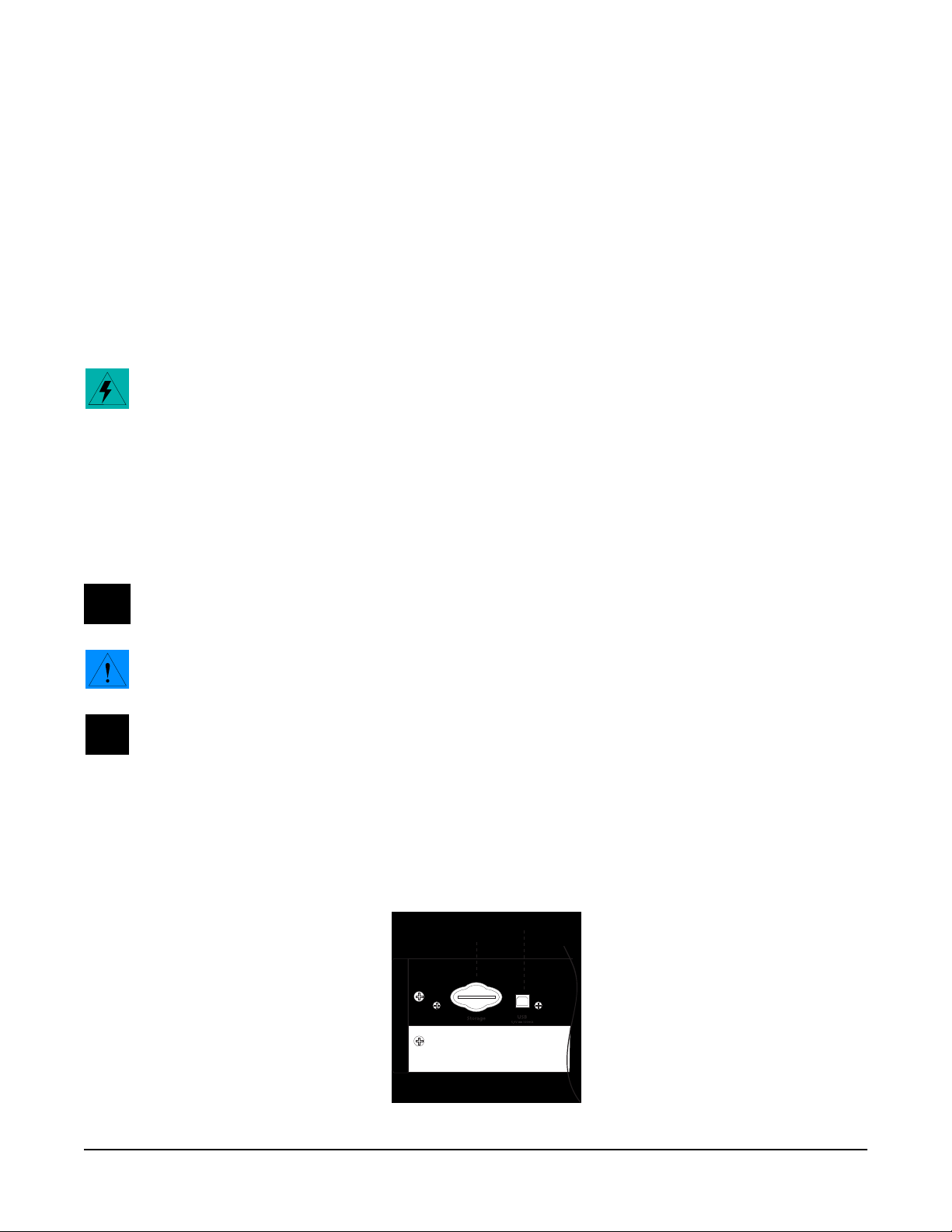
The lightning flash with the arrowhead symbol,
CAUTION
RISK OF ELECTRIC SHOCK
DO NOT OPEN
within an equilateral triangle, is intended to alert
the user to the presence of uninsulated
"dangerous voltage" within the product's
enclosure that may be of sufficient magnitude
to constitute a risk of electric shock to persons.
CAUTION: TO REDUCE THE RISK OF ELECTRIC SHOCK,
DO NOT REMOVE THE COVER
NO USER SERVICEABLE PARTS INSIDE
REFER SERVICING TO QUALIFIED SERVICE PERSONNEL
The exclamation point within an equilateral
triangle is intended to alert the user to the
presence of important operating and
maintenance (servicing) instructions in the
literature accompanying the product.
IMPORTANT SAFETY & INSTALLATION INSTRUCTIONS
INSTRUCTIONS PERTAINING TO THE RISK OF FIRE, ELECTRIC SHOCK, OR INJURY TO PERSONS
WARNING: When using electric products, basic precautions should
always be followed, including the following:
1. Read all of the Safety and Installation Instructions and Explanation
of Graphic Symbols before using the product.
2. This product must be grounded. If it should malfunction or break
down, grounding provides a path of least resistance for electric
current to reduce the risk of electric shock. This product is equipped
with a power supply cord having an equipment-grounding
conductor and a grounding plug. The plug must be plugged into an
appropriate outlet which is properly installed and grounded in
accordance with all local codes and ordinances.
DANGER: Improper connection of the equipment-grounding
conductor can result in a risk of electric shock. Do not modify the
plug provided with the product - if it will not fit the outlet, have a
proper outlet installed by a qualified electrician. Do not use an
adaptor which defeats the function of the equipment-grounding
conductor. If you are in doubt as to whether the product is properly
grounded, check with a qualified serviceman or electrician.
3. WARNING: This product is equipped with an AC input voltage
selector. The voltage selector has been factory set for the mains
supply voltage in the country where this unit was sold. Changing
the voltage selector may require the use of a different power supply
cord or attachment plug, or both. To reduce the risk of fire or electric
shock, refer servicing to qualified maintenance personnel.
4. Do not use this product near water - for example, near a bathtub,
washbowl, kitchen sink, in a wet basement, or near a swimming
pool, or the like.
5. This product should be used only with a stand or cart that is
recommended by the manufacturer.
6. This product, either alone or in combination with an amplifier and
speakers or headphones, may be capable of producing sound
levels that could cause permanent hearing loss. Do not operate for
a long period of time at a high volume level or at a level that is
uncomfortable. If you experience any hearing loss or ringing in the
ears, you should consult an audiologist.
7. The product should be located so that its location or position does
not interfere with its proper ventilation.
8. The product should be located away from heat sources such as
radiators, heat registers, or other products that produce heat.
9. The product should be connected to a power supply only of the type
described in the operating instructions or as marked on the product.
10. This product may be equipped with a polarized line plug (one blade
wider than the other). This is a safety feature. If you are unable to
insert the plug into the outlet, contact an electrician to replace your
obsolete outlet. Do not defeat the safety purpose of the plug.
11. The power supply cord of the product should be unplugged from the
outlet when left unused for a long period of time. When unplugging
the power supply cord, do not pull on the cord, but grasp it by the
plug.
12. Care should be taken so that objects do not fall and liquids are not
spilled into the enclosure through openings.
13. The product should be serviced by qualified service personnel
when:
A. The power supply cord or the plug has been damaged;
B. Objects have fallen onto, or liquid has been spilled into the
product;
C. The product has been exposed to rain;
D. The product does not appear to be operating normally or
exhibits a marked change in performance;
E. The product has been dropped, or the enclosure damaged.
14. Do not attempt to service the product beyond that described in the
user maintenance instructions. All other servicing should be
referred to qualified service personnel.
WARNING: Do not place objects on the product’s power supply
15.
cord, or place the product in a position where anyone could trip
over, walk on, or roll anything over cords of any type. Do not allow
the product to rest on or be installed over cords of any type.
Improper installations of this type create the possibility of a fire
hazard and/or personal injury.
RADIO AND TELEVISION INTERFERENCE
WARNING: Changes or modifications to this instrument not expressly
approved by Young Chang could void your authority to operate the
instrument.
IMPORTANT: When connecting this product to accessories and/or other
equipment use only high quality shielded cables.
NOTE: This instrument has been tested and found to comply with the
limits for a Class B digital device, pursuant to Part 15 of the FCC Rules.
These limits are designed to provide reasonable protection against
harmful interference in a residential installation. This instrument
generates, uses, and can radiate radio frequency energy and, if not
installed and used in accordance with the instructions, may cause
harmful interference to radio communications. However, there is no
guarantee that interference will not occur in a particular installation. If
this instrument does cause harmful interference to radio or television
reception, which can be determined by turning the instrument off and on,
the user is encouraged to try to correct the interference by one or more
of the following measures:
SAVE THESE INSTRUCTIONS
ii
• Reorient or relocate the receiving antenna.
• Increase the separation between the instrument and the receiver.
• Connect the instrument into an outlet on a circuit other than the one
to which the receiver is connected.
• If necessary consult your dealer or an experienced radio/television
technician for additional suggestions.
NOTICE
This apparatus does not exceed the Class B limits for radio noise
emissions from digital apparatus set out in the Radio Interference
Regulations of the Canadian Department of Communications.
AVIS
Le present appareil numerique n’emet pas de bruits radioelectriques
depassant les limites applicables aux appareils numeriques de la
class B prescrites dans le Reglement sur le brouillage radioelectrique
edicte par le ministere des Communications du Canada.
Page 3

Important Safety Instructions
1. Read these instructions.
2. Keep these instructions.
3. Heed all warnings.
4. Follow all instructions.
5. Do not use this apparatus near water.
6. Clean only with dry cloth.
7. Do not block any of the ventilation openings. Install in accordance with the manufacturer’s
instructions.
8. Do not install near any heat sources such as radiators, heat registers, stoves, or other apparatus
(including amplifiers) that produce heat.
9. Do not defeat the safety purpose of the polarized or grounding-type plug. A polarized plug has
two blades with one wider than the other. A grounding type plug has two blades and a third
grounding prong. The wide blade or the third prong are provided for your safety. If the
provided plug does not fit into your outlet, consult an electrician for replacement of the obsolete
outlet.
10. Protect the power cord from being walked on or pinched, particularly at plugs, convenience
receptacles, and the point where they exit from the apparatus.
11. Only use attachments/accessories specified by the manufacturer.
12. Use only with a cart, stand, tripod, bracket, or table specified by the
manufacturer, or sold with the apparatus. When a cart is used, use
caution when moving the cart/apparatus combination to avoid
injury from tip-over.
13. Unplug this apparatus during lightning storms or when unused for
long periods of time.
14. CAUTION: Danger of explosion if battery is incorrectly replaced. Replace only with the same or
equivalent type (CR2032).
15. Refer all servicing to qualified service personnel. Servicing is required when the apparatus has
been damaged in any way, such as power supply cord or plug is damaged, liquid has been
spilled or objects have fallen into the apparatus, the apparatus has been exposed to rain or
moisture, does not operate normally, or has been dropped.
Warning - To reduce the risk of fire or electric shock, do not expose this apparatus to rain or moisture.
Do not expose this equipment to dripping or splashing and ensure that no objects filled with liquids,
such as vases, are placed on the equipment.
To completely disconnect this equipment from the AC Mains, disconnect the power supply cord plug
from the AC receptacle.
iii
Page 4

Kurzweil International Contacts
Contact the Kurzweil office listed below to locate your local Kurzweil representative.
Kurzweil Music Systems
19060 S. Dominies Hills Drive
Rancho Dominguez
California 90220 USA
Telephone: (310) 637-2000
Fax: (310) 637-2025
http://www.kurzweilmusicsystems.com
Kurzweil Co., LTD
iPark Building #102, Floor 9
Jeongja-Dong 9, Bundang-Gu
Soungnam-Shi, Gyeonggi-Do 463-859
South Korea
http://www.ycpiano.co.kr
http://www.youngchang.com
Page 5

Kurzweil PC3x Service Manual
Chapter 1 Introduction
Notes, Cautions, Warnings ............................................................................................................................................ 1-1
Rear Panel Features......................................................................................................................................................... 1-1
PC3x Front Panel............................................................................................................................................................. 1-3
Front Panel Features................................................................................................................................................ 1-3
Wheels Assembly (not shown)........................................................................................................................ 1-5
Chapter 2 Diagnostics
Diagnostic Tests ............................................................................................................................................................... 2-1
Entering Diagnostics....................................................................................................................................................... 2-1
LCD and Front Panel Buttons ................................................................................................................................ 2-2
Test Results................................................................................................................................................................ 2-2
Diagnostic Test Modes.................................................................................................................................................... 2-3
Run ............................................................................................................................................................................. 2-3
Loop ........................................................................................................................................................................... 2-3
Continuous................................................................................................................................................................ 2-3
Burn-in loop.............................................................................................................................................................. 2-3
Description of Tests......................................................................................................................................................... 2-4
SDRAM Refresh ....................................................................................................................................................... 2-4
Flash Memory........................................................................................................................................................... 2-4
MARA Validity Check ............................................................................................................................................. 2-4
MARA Communications......................................................................................................................................... 2-4
Expansion DIMM Check......................................................................................................................................... 2-5
MIDI UART............................................................................................................................................................... 2-5
External Card............................................................................................................................................................ 2-6
MARA Delay RAM.................................................................................................................................................. 2-6
MARA Sound ROM................................................................................................................................................. 2-6
Audio Output ........................................................................................................................................................... 2-7
Diagnostic Version 0.20 or earlier................................................................................................................... 2-7
Sine Wave Test................................................................................................................................................... 2-8
Chapter 3 Disassembly/Assembly
Introduction ..................................................................................................................................................................... 3-1
Notes, Cautions, Warnings ..................................................................................................................................... 3-1
Cables, Connectors................................................................................................................................................... 3-1
Cables ................................................................................................................................................................. 3-1
Cable Routing.................................................................................................................................................... 3-1
Required Tools and Materials................................................................................................................................. 3-1
Opening the PC3x ........................................................................................................................................................... 3-2
PC3x Bottom ............................................................................................................................................................. 3-2
Removing the Top Enclosure.................................................................................................................................. 3-3
Replacing the Top Enclosure .................................................................................................................................. 3-5
Closing the PC3x ...................................................................................................................................................... 3-6
Top Enclosure................................................................................................................................................................... 3-7
Removing the Enclosure Support Wall................................................................................................................. 3-8
Replacing the Enclosure Support Wall.................................................................................................................. 3-8
Removing the Connector Board............................................................................................................................. 3-9
Replacing the Connector Board ........................................................................................................................... 3-10
Removing the Slider Board....................................................................................................................................3-11
Replacing the Slider Board ................................................................................................................................... 3-12
i
Page 6

Kurzweil PC3x Service Manual
Removing the LCD Board..................................................................................................................................... 3-13
Replacing the LCD Board ..................................................................................................................................... 3-14
Removing the Front Panel Board......................................................................................................................... 3-14
Replacing the Front Panel Board ......................................................................................................................... 3-16
Removing the Engine Board................................................................................................................................. 3-17
Replacing the Engine Board ................................................................................................................................. 3-18
Removing the USB/xD Daughtercard................................................................................................................ 3-18
Replacing the USB/xD Daughtercard................................................................................................................. 3-18
Removing the Wheels Assembly ......................................................................................................................... 3-19
Replacing the Wheels Assembly.......................................................................................................................... 3-19
PC3x Keyboard Assembly............................................................................................................................................ 3-20
Removing the PC3x Keyboard Assembly........................................................................................................... 3-20
Replacing the PC3x Keyboard Assembly........................................................................................................... 3-21
Removing Keys ...................................................................................................................................................... 3-22
Natural/White Key ........................................................................................................................................ 3-22
Removing Natural/White Keys........................................................................................................................... 3-23
Removing Sharp/Black Keys ............................................................................................................................... 3-23
Replacing a Sharp Key .......................................................................................................................................... 3-23
Replacing a Natural/White Key.......................................................................................................................... 3-24
Servicing the Keyboard Contact Boards............................................................................................................. 3-24
Removing the Treble Contact Board ............................................................................................................ 3-24
Replacing the Treble Contact Board............................................................................................................. 3-24
Removing the Bass Contact Board ............................................................................................................... 3-24
Replacing the Bass Contact Board................................................................................................................ 3-25
Connecting the Keyboard Contact Boards ......................................................................................................... 3-25
Removing the Keyboard Contact Strips ............................................................................................................. 3-25
Replacing the Keyboard Contact Strips.............................................................................................................. 3-25
Chapter 4 Troubleshooting & Maintenance
Introduction ..................................................................................................................................................................... 4-1
Cables, Connectors................................................................................................................................................... 4-1
Cables ................................................................................................................................................................. 4-1
Cable Routing.................................................................................................................................................... 4-1
Surface-Mount Devices ........................................................................................................................................... 4-1
Required Tools and Materials................................................................................................................................. 4-1
Boot Loader...................................................................................................................................................................... 4-2
Entering the Boot Loader........................................................................................................................................ 4-2
Resets................................................................................................................................................................................. 4-2
Hard Reset................................................................................................................................................................. 4-2
Soft Reset ................................................................................................................................................................... 4-2
Saving User Data............................................................................................................................................................. 4-3
Saving to an xD Card............................................................................................................................................... 4-3
Saving to a Computer.............................................................................................................................................. 4-3
Software Updates ............................................................................................................................................................ 4-4
Updating with an xD Card ..................................................................................................................................... 4-4
Updating via Computer.......................................................................................................................................... 4-5
Rebuilding the Internal NAND Flash Memory.......................................................................................................... 4-6
Rebuilding with an xD Card .................................................................................................................................. 4-6
Rebuilding via a Computer .................................................................................................................................... 4-7
Boot EPROM .................................................................................................................................................................... 4-9
Removing the EPROM ............................................................................................................................................ 4-9
ii
Page 7

Kurzweil PC3x Service Manual
Replacing the EPROM............................................................................................................................................. 4-9
Replacing the Battery.................................................................................................................................................... 4-10
Accessing the Battery............................................................................................................................................. 4-10
Removing the Battery............................................................................................................................................ 4-10
Installing the Battery ............................................................................................................................................. 4-10
Scanner Tests...................................................................................................................................................................4-11
Front Panel Buttons ................................................................................................................................................4-11
Alpha Wheel ........................................................................................................................................................... 4-12
Front Panel Sliders................................................................................................................................................. 4-12
Right Main Output................................................................................................................................................. 4-12
Switch Pedals 1, 2, and 3 ....................................................................................................................................... 4-12
Continuous Control Pedal 1 and 2 ...................................................................................................................... 4-12
Wheels ..................................................................................................................................................................... 4-13
Adjusting the Pitch Wheel Center................................................................................................................ 4-13
Keyboard ................................................................................................................................................................. 4-13
Adjusting Key Pressure Sensitivity.............................................................................................................. 4-13
Power Problems............................................................................................................................................................. 4-14
Dead: LEDs, LCD backlight, and xD Card socket not lit ................................................................................. 4-14
Audio Problems............................................................................................................................................................. 4-14
No Audio................................................................................................................................................................. 4-14
Front Panel Problems.................................................................................................................................................... 4-15
LCD not lit............................................................................................................................................................... 4-15
LCD lit, no characters ............................................................................................................................................ 4-15
Buttons, Sliders or Controllers not working ...................................................................................................... 4-15
Keyboard Problems....................................................................................................................................................... 4-16
Dead Keyboard....................................................................................................................................................... 4-16
Dead Note(s) or no velocity sensitivity .............................................................................................................. 4-16
One or More in a Section................................................................................................................................ 4-16
PC3x Interconnect Diagram......................................................................................................................................... 4-17
Converting the Voltage................................................................................................................................................. 4-18
Accessing the Fuses ............................................................................................................................................... 4-18
The Fuse Holder..................................................................................................................................................... 4-19
Using 5 mm X 20 mm Fuses .......................................................................................................................... 4-21
Replacing the Fuse Holder ................................................................................................................................... 4-21
Chapter 5 Parts Lists
PCB & Sub Assemblies............................................................................................................................................ 5-1
Engine Board............................................................................................................................................................. 5-1
Connector Board ...................................................................................................................................................... 5-4
Front Panel Board..................................................................................................................................................... 5-6
Slider Board............................................................................................................................................................... 5-7
Engine Board–USB/xD Daughtercard.................................................................................................................. 5-7
Button Board............................................................................................................................................................. 5-8
Wheels Assembly..................................................................................................................................................... 5-8
Keyboard Assembly................................................................................................................................................. 5-8
Miscellaneous ........................................................................................................................................................... 5-9
Chapter 6 Schematics
Engine Board Assembly–SH7705 CPU and Memory (1 of 9) ................................................................................... 6-3
Engine Board Assembly–MARA 2 (2 of 9)................................................................................................................... 6-4
iii
Page 8

Kurzweil PC3x Service Manual
Engine Board Assembly–MARA 1 (3 of 9)................................................................................................................... 6-5
Engine Board Assembly–MARA Clocks, Delay Memory Interface (4 of 9)............................................................ 6-6
Engine Board Assembly–Sound ROM (5 of 9)............................................................................................................ 6-7
Engine Board Assembly–ROM DIMMs, SmartMedia Interface, LCD, etc. (6 of 9)............................................... 6-8
Engine Board Assembly–DAC, Main Outs (7 of 9) .................................................................................................... 6-9
Engine Board Assembly–Aux and Headphone Outs (8 of 9) ................................................................................. 6-10
Engine Board Assembly–Mictors, CPLD, Power (9 of 9) .........................................................................................6-11
Connector Board–M38869 Scanner (1 of 4)................................................................................................................ 6-12
Connector Board–MIDI, Pedals, Ribbon, LCD Contrast (2 of 4)............................................................................ 6-13
Connector Board–Power Supply, Audio (3 of 4)....................................................................................................... 6-14
Connector Board–Sample Rate Converter (4 of 4).................................................................................................... 6-15
Front Panel Board–Front Panel Misc. Buttons And LEDs (1 of 2).......................................................................... 6-16
Front Panel Board–Front Panel Bank & Program Buttons & LEDs (2 of 2) .......................................................... 6-17
Slider Board.................................................................................................................................................................... 6-18
Wheels Board–Wheels & AT........................................................................................................................................ 6-19
Engine Board–USB/xD Daughtercard....................................................................................................................... 6-20
i
v
Page 9
Chapter 1
Introduction
This chapter provides the service technician with a layout of the front and rear panel features, as
well as a brief explanation of their functions. For in-depth descriptions of the many features the
PC3x includes, consult the Getting Started Guide .
Warning : If possible, save all user programs and setups before disassembly. For instructions,
refer to the Boot Loader in Chapter 4, page 4-2 .
Notes, Cautions, Warnings
Please pay special attention to all Notes, Cautions, and Warnings used throughout this manual
as they not only point out specific instructions, but also alert you to variations between
manufactured units.
A brief description of these symbols follows:
Note : Provides additional information, indicates differences between models, and emphasizes
specific instructions.
Caution : Highlights areas to instruct you to proceed cautiously so that damage does not occur
to the unit or individual components.
Warning : Alerts you so that damage does not occur to yourself, others, or external equipment
and devices.
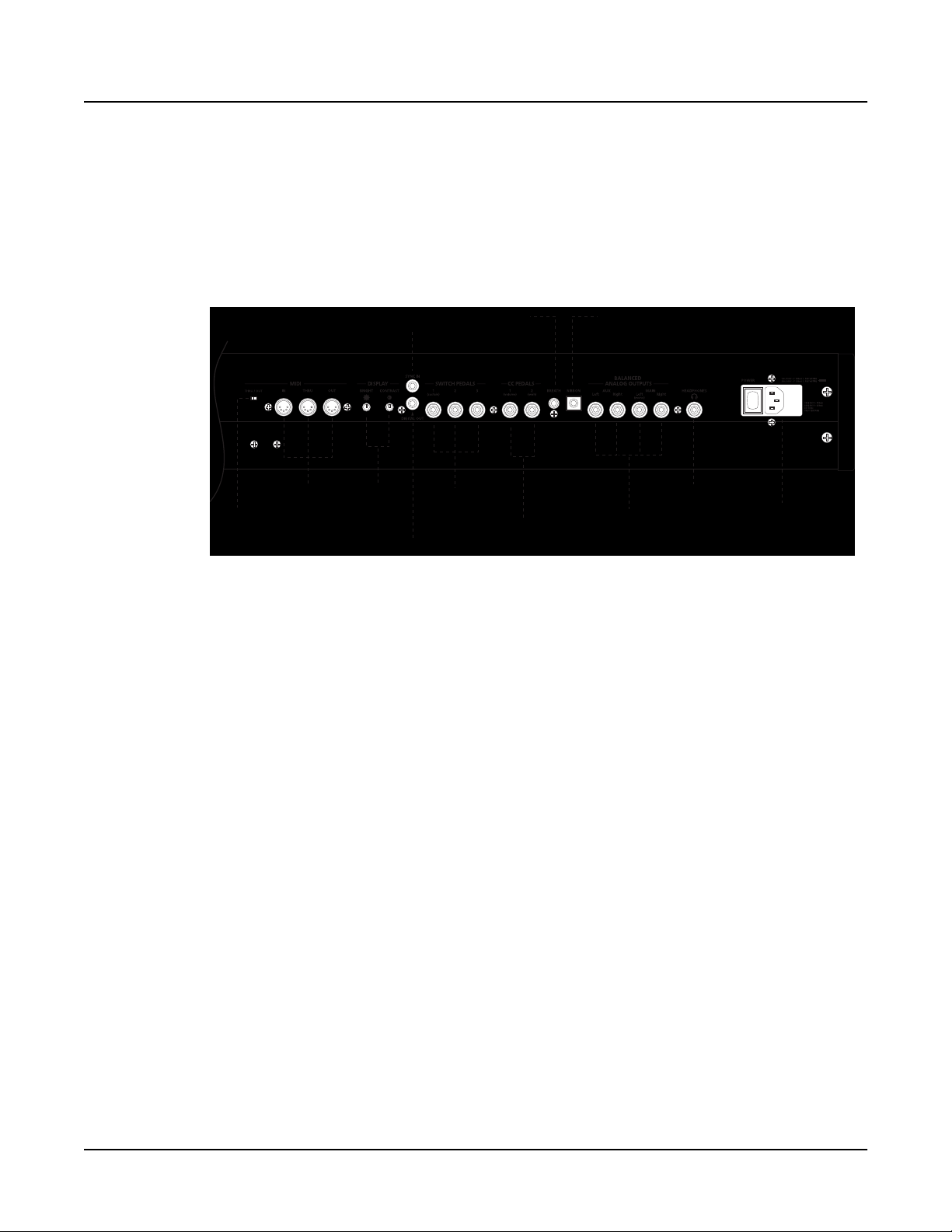
Rear Panel Features
Storage —Use this slot to insert an xD memory card to update software, back up, and share files.
USB Port —Use the USB Port to send and receive MIDI or to connect to a computer for file
transfer.
Storage
Figure 1-1 PC3x rear panel, left end
USB Port
1-1
Page 10
Introduction
Rear Panel Features
MIDI Select Switch —Slide switch to select the operation of the MIDI Thru/Out port. This
switch is recessed into the rear panel so that it cannot be accidentally changed.
MIDI Ports —In, Thru/Out, and Out ports to connect the PC3x to other MIDI devices to receive,
pass, and send MIDI data.
Display —Rotary potentiometers to adjust the brightness and contrast of the LCD for the best
visibility.
MIDI
Select
Switch
MIDI
Ports
Display
Bright,
Contrast
Sync In
Digital Out
Breath
Input
Switch
Pedals
Continuous
Control Pedals
Ribbon
Input
Balanced
Analog Outputs
Headphones
Power Entry
Module
Figure 1-2 PC3x rear panel, right end
Sync In —This RCA jack allows the PC3x to receive digital clock signals when it is slaved to
another device.
Digital Out —RCA jack to connect to another device with an AES or S/PDIF input via a 75 !
coaxial cable.
Switch Pedals —Three 1/4” jacks to connect switch pedals that can be assigned to control
operations such as sustain, sostenuto, etc. (use 1/4” tip/sleeve).
1-2
Continuous Control Pedals —Two 1/4” jacks to connect pedals that can be assigned to control
operations such as volume, expression, etc. (use 10K ! linear taper potentiometer, 1/4”
tip/ring/sleeve, wiper to tip).
Breath Input —A 3.5mm jack to connect a standard breath controller to send standard MIDI
Breath messages.
Ribbon Input —Modular jack to connect the Kurzweil Ribbon Controller option.
Balanced Analog Outputs —Four 1/4” balanced audio output jacks. Use the Main outputs, left
(mono) and right, to connect to an amplifier, mixer or sound system. Use the Aux outputs for
monitoring or other operations. They duplicate the Main outputs, but are always in stereo.
Headphones —Standard 1/4” jack to connect headphones.
Power Entry Module —includes the power switch, AC receptacle, and the fuse holder/voltage
select compartment. (See Chapter 4, page 4-18 for instructions to change the voltage setting.)
Page 11
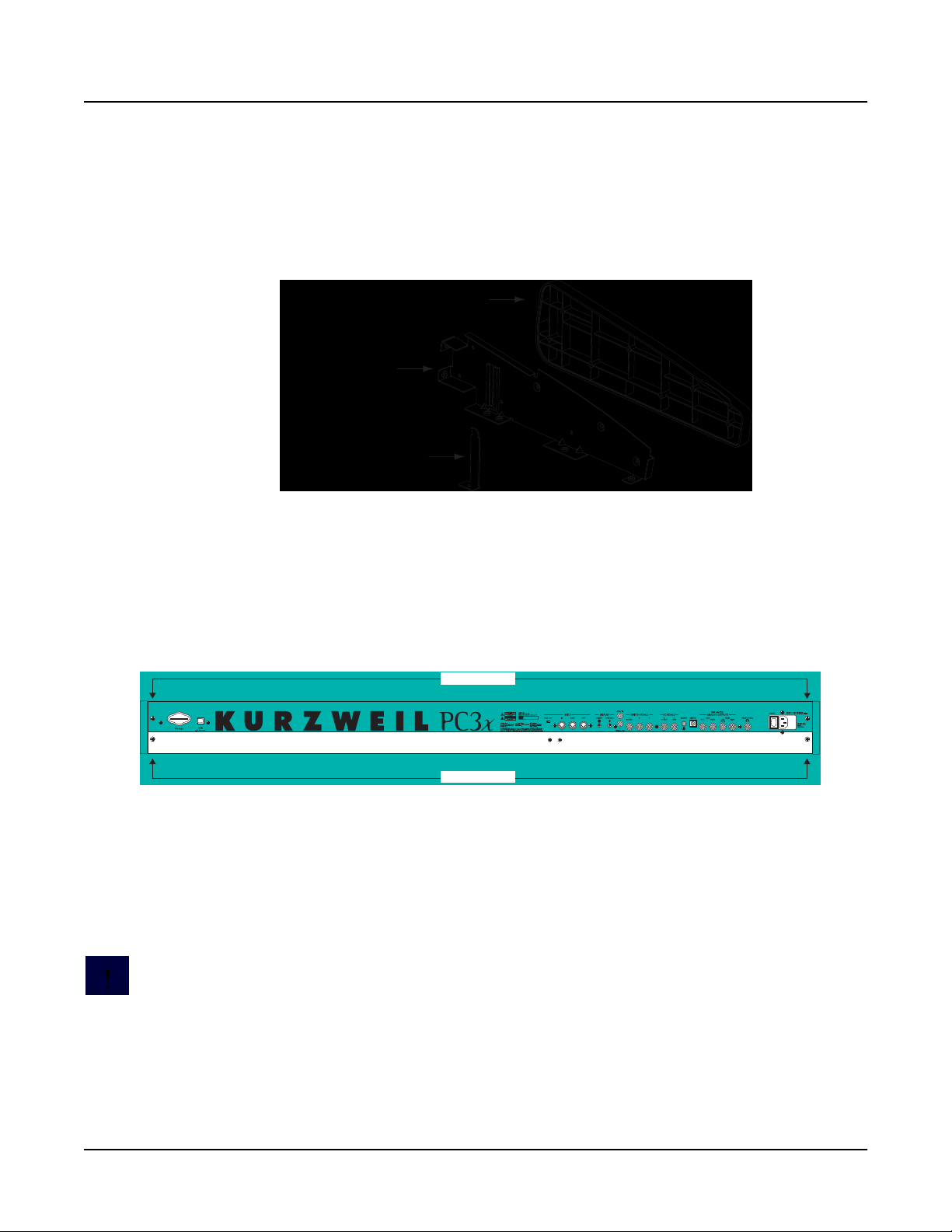
PC3x Front Panel
V
y
p
Front Panel Features
Introduction
PC3x Front Panel
MASTER
OLUME
BANKS
StringsOrchestraClassic KeysBase 1 Base 2 Exp 1 UserExp 2
Rotary
16' 5 1/3' 8' 4' 2 2/3' 2' 1 3/5' 1 1/3' 1'
A B IEC G HFD
Data MIDI 1 3 MIDI 22 MI DI 23 MIDI 24
Vibrato
DepthOn/Off Chor/VibFast/Slow
Loud/Soft Decay F/S Pitch H/L
On /Off
Percussion Enable
MIDI 25 MIDI 26 MIDI 27 MIDI 28
KB3
On /Off
Figure 1-3 Master Volume, Bank buttons, Sliders
Master Volume —Slider to adjust the overall volume.
Bank buttons—Use these buttons to select different banks of programs, then select an individual
program using the Category and Program buttons. The labeling above the button indicates the
program. In KB3 mode, these buttons have different functions. Their labeling is below the Bank
buttons.
Sliders —The operation of the sliders depends on which mode is active. In KB3 mode, these
sliders emulate the drawbars of an organ. They are labeled as follows: above each slider for KB3
mode, and below when used for data and MIDI controllers.
MODE
MIDIProgram
Mute 1
Setup Master
Q Access Song
Solo Mute Active
Effect Storage
FX Bypass Compare
Record Pla
Mute 2
Mute 4Mute 3
/ Pause Sto
Chan / Layer
Edit
Figure 1-4 Mode, Edit, Chan/Layer and record function buttons
Mode buttons—use these buttons to select one of the eight available operating modes. The
additional labeling of these buttons indicate that they function differently depending on the
current mode or editor.
1-3
Page 12
Introduction
PC3x Front Panel
Chan/Layer buttons—depending on the current editor, use these buttons to scroll through
layers, presets, values, and zones.
Record , Play/Pause , and Stop buttons—use these buttons to activate the sequencer to record
and playback songs.
Edit button—use this button to enter the editor or the current mode to modify a selected object
or parameter.
ExitExit
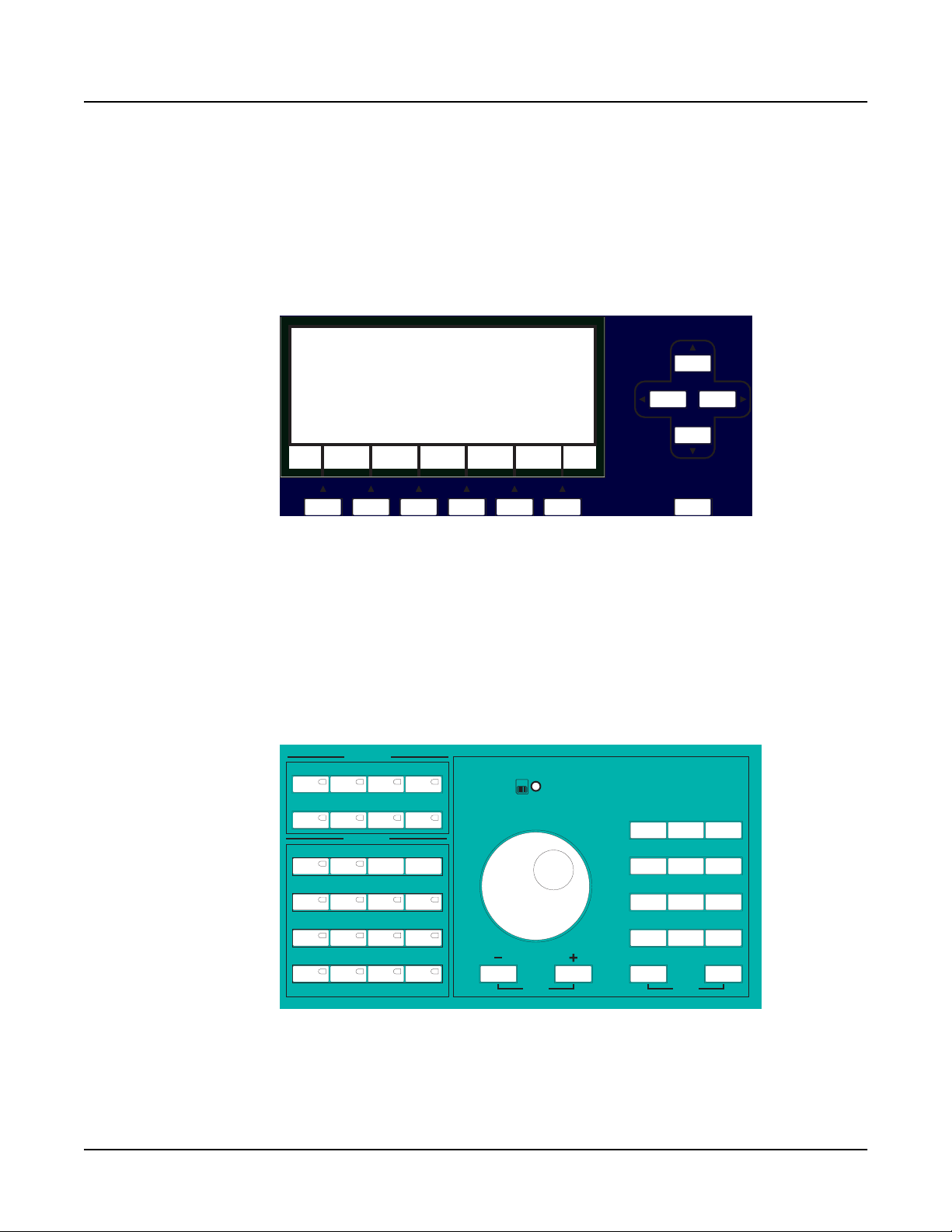
Figure 1-5 LCD and Soft, Cursor, and Exit buttons
Display —Angled 240 x 64, backlit graphic LCD.
Soft buttons — use these buttons to select an action or item shown directly above the button in
the bottom line of the display.
Cursor buttons — use these buttons navigate the cursor in the display.
Exit button—press this button to leave the current editor.
PROGRAM
1 432
CATEGORY
E Piano 1Piano 2Piano 1 E Piano 2
8765
BrassOrganClavierPop Keys
PadsSynthsVoicesStrings
PercussionDrumsBassGuitar
Jump
Storage
Active
1 2 3
4 5 6
STU YZVWX
-
/
+
Shift 0-9
Cancel Enter
GHIDEFABC
PQRMNOJKL
8 97
0 Clear
Space
PANIC
1-4
Figure 1-6 Program, Category, Alpha wheel and Alphanumeric buttons
Category and Program buttons—use these buttons to first select a Category , then select one of
the eight
Program buttons.
Page 13

PC3x Front Panel
Alpha Wheel— use the Alpha Wheel to increase or decrease a value by one or several
increments.
Plus ( + ) and Minus ( – ) buttons —these buttons operate similar to the Alpha Wheel. Pressing the
Plus (+) or Minus (-) button allows you to increase or decrease a value by one. Pressing these
buttons simultaneously, selects the Jump function.
Alphanumeric Keypad—use these buttons to enter characters (both uppercase and lowercase),
numbers, and spaces. Pressing these buttons simultaneously, selects the Panic button. Select the
Panic button to send an All Notes/All Controllers Off message on all 16 channels.
Storage Active LED—this blue LED is lit when an xD daughter card is installed and there is
activity. (Do not remove the xD card when the blue LED is lit.)
Wheels Assembly (not shown)
Pitch and Mod Wheels—use these wheels to vary modulation and pitch. In some programs, the
Mod Wheel can be used for other functions.
Introduction
ARP button—use this button to active the Arpeggiator.
SW button—this button can be programmed for a variety of functions.
1-5
Page 14

Introduction
PC3x Front Panel
1-6
Page 15

Chapter 2
Diagnostics
Diagnostic Tests
The following lists the diagnostic tests available for the PC3x.
Note: Throughout this manual many references are made to the MARA 1 and MARA 2 ICs. For
service personnel unfamiliar with the PC3x, MARA is the name given to the two Kurzweil
Custom Sound ICs.
• SDRAM Refresh
• Flash Memory
• MARA Validity Check
• MARA Communications
• Exp DIMM Check
• MIDI UART
• External Card
• MARA Delay RAM
• MARA Sound ROM
• Audio Output
Warning: If possible, save all user programs and setups before entering diagnostics or
performing maintenance or repair. For instructions, refer to Saving User Data in Chapter 4,
page 4-2.
Entering Diagnostics
1. Apply power to the unit. When the ****Welcome to the Kurzweil PC3**** message appears in
the LCD, quickly press and release the Exit button. The LCD should display the following:
PC3 Boot Loader Version X.XX
RUN UPDATE RUN SYSTEM FILE
PC3 IMAGE DIAGS RESET UTILITIES
Figure 2-1 LCD example, Boot Loader
2. Press the soft button below RUN DIAGS in the LCD.
2-1
Page 16

Diagnostics
Entering Diagnostics
3. The LCD flashes the message: Running ROM-based diagnostics.
4. The LCD displays the following:
Running SDRAM refresh test
RAM Test Passed
OK
Figure 2-2 LCD example, diagnostic main menu
5. The bottom line in the display shows the four test modes. Press the soft button below the
test mode to run the tests.
LCD and Front Panel Buttons
The LCD displays the list of tests, test modes, actions, and test results.
Press the Left, Right, Up, or Down cursor buttons or turn the Alpha Wheel to navigate through
the available tests.
Use the soft buttons located below the LCD to select different test modes or actions.
Press the Exit button to return to the Boot Loader.
Test Results
At the completion of an individual test, the LCD displays the results of the test. Figure 2-3 shows
an example of the display for the SDRAM refresh test.
Figure 2-3 LCD example, SDRAM refresh test
Running SDRAM refresh test
RAM Test Passed
OK
2-2
Page 17

Diagnostic Test Modes
Run
The run test mode allows you to select an individual test, or to step through and run each
available test. To step through the different tests, use the Left, Right, Up, or Down cursor
buttons or turn the Alpha Wheel. Press the soft button below RUN to select the test.
At the completion of a test, whether pass or fail, press the OK soft button to exit the test and
return to the test menu.
To exit diagnostics, press the Exit button to return to the Boot Loader.
Loop
Loop continuously runs an individual test. The number of tests performed and the result is
displayed continuously in the LCD. The test continues to run until you press the Exit button.
Continuous
Continuous is the same as Loop, but stops if a failure is detected.
Diagnostics
Diagnostic Test Modes
Burn-in loop
Burn-in continuously runs the following sequence of tests.
• SDRAM Refresh
• Flash Memory
• MARA Validity Check
• MARA Delay RAM
• MARA Communications
• MARA Sound ROM
If a failure is detected, the test stops and displays the result.
To exit Run Burn-in and return to the Boot Loader, press and hold the Exit button.
2-3
Page 18

Diagnostics
Description of Tests
Description of Tests
SDRAM Refresh
This test verifies the write/read functionality and accuracy of the SDRAM chip (U3) attached to
the microprocessor, SH7705 (U1).
A failure of this test indicates a problem with the SDRAM chip or associated circuitry on the
Engine Board.
Flash Memory
This test verifies the manufacturer ID and the size of the NAND Flash installed. The test then
writes and reads back one or more blocks not occupied by the file system. This test also indicates
if the NAND Flash is formatted or unformatted.
A failure of this test may indicate a problem with the with the microprocessor (U1), NAND
Flash (U2), Fin CPLD (U45), or related circuitry on the Engine Board.
MARA Validity Check
Note: Throughout this manual many references are made to the MARA 1 and MARA 2 ICs. For
service personnel unfamiliar with the PC3x, MARA is the name given to the two Kurzweil
Custom Sound ICs.
This tests verifies the proper content of certain read-only registers and the read/write accuracy
of certain read/write registers on both MARAs. It also writes and reads back the various register
blocks in both MARAs that are implemented as RAM cells.
A failure of this test may indicate a problem with the with the microprocessor (U1), MARA 1
(U11) or MARA 2 (U10), or related circuitry on the Engine Board.
MARA Communications
This test transfers data from one MARA to the other via the SMOOCH interface and checks the
accuracy of the data received. All four SMOOCH inputs and outputs are exercised.
This test will likely fail if the MARA Validity Test fails. However if the MARA Validity Test
passes and this test fails, it may indicate a bad solder joint underneath one or both MARAs.
2-4
Page 19

Expansion DIMM Check
This test checks to see if a DIMM module is installed in J10 or J11 and confirms the type.
Running Exp DIMM check test
CHECK READ WRITE PLAY
DIMMS DIMMS DIMMS DIMMS EXIT
Figure 2-4 LCD example, Exp DIMM check test
Note: There are two types of DIMM modules—one with all four NOR Flash chips present and
the other with only two out of the four chips populated. The J10 DIMM socket on the Engine
Board can only support the half-populated DIMM version.
Each DIMM module has an upper and lower bank. The half-populated DIMM module has Flash
chips installed in the upper bank only. Therefore, this diagnostic will only report results for
DIMM 0, High Bank; but will report results for both the High and Low Bank of DIMM 1.
Diagnostics
Description of Tests
A failure of this test may indicate a problem with the DIMM(s), their installation, soldering of
the socket(s), or related circuitry on the Engine Board.
MIDI UART
The MIDI test performs a loop-back of the serial port by sending a 23-byte pattern over the
external MIDI link. This test requires a MIDI loop (a MIDI cable that connects two MIDI jacks).
The test will fail if a MIDI cable is not connected between two MIDI jacks. Be sure to run this test
with MIDI cables connected as follows:
1. Connect a MIDI cable to the MIDI In and MIDI Out jacks and run the test.
2. Connect a MIDI cable to the MIDI In and MIDI Out/Thru jacks and set the MIDI select
A failure of this test could be caused by failure of the serial port, other MIDI circuitry, or a
problem on the Engine Board.
On the Engine Board check the signal paths from U1, pins 172, 174, 177, and 179 to connector J5.
switch on the rear panel to Out. Run the test.
2-5
Page 20

Diagnostics
Description of Tests
External Card
This test checks the hardware interface for the xD Card. The test first checks to see if a card is
installed; and if so, reads and reports the identifying data.
Note: This test is safe to run on an xD Card that has data on it.
A failure of this test indicates a problem with USB/xD Daughtercard, related circuitry or the
Engine Board.
MARA Delay RAM
This is a write/read test to check the Delay RAM connected to MARA 1. The Delay RAM test
first checks address and databus connectivity and then reports which bits are not functioning to
aid troubleshooting.
Error reporting for this test identifies whether the error is likely to have occurred during writing
or during reading. Data value mismatch errors are reported in hexadecimal values starting with
“0x” followed by 8 hex digits. If the data value that was ReadBack differs greatly from the value
Wrote, it could mean there was an address bit error, or one or more of the control signals are bad.
A failure of this test would indicate a problem with the DDR SDRAM (U13), MARA 1 (U11), or
the Engine Board.
MARA Sound ROM
This test calculates and verifies the checksum for each 16 MB section of the on-board Sound
(Sample) ROM. It also tests the data and address lines from both MARAs to the Sound ROMs.
This test may also report errors when the MARA Validity Test fails. If MARA Validity Test only
fails on one of the MARAs, then the other MARA may still pass this test.
Running MARA sound ROM test
MARA 1 Sound ROM checksums are correct
MARA 1 Sound ROM data lines are correct
MARA 1 Sound ROM addr lines are correct
MARA 2 Sound ROM checksums are correct
MARA 2 Sound ROM data lines are correct
OK
Figure 2-5 LCD example, MARA Sound ROM test
A failure of this test may indicate a problem with a Sound ROMs (U20, U21, U22, or U23), or the
Engine Board.
Use the Down cursor button
or the Alpha wheel to scroll
down to the next line of the
test result.
2-6
Page 21

Audio Output
This is not a test that fails. It is an interactive test for the entire audio chain. However for this test
to pass reliably, the MARA Validity and MARA Delay RAM tests should pass. The software
creates waveforms (sine and sawtooth) and stores them in the Delay RAM. Therefore, MARA 1
and its Delay RAM need to be functioning for this test to produce a clean audio waveform.
When you select this test, the LCD displays the following:
Figure 2-6 LCD example, Audio output test
Note: If the diagnostic version is earlier than 0.20, this test is only useful to check the polarity of
the Main Output audio signals. Use the Sine Wave Test on page 2-8 for audio level and distortion
tests. If the diagnostic version is 0.20 or later, follow the on-screen instructions for use.
Diagnostics
Description of Tests
Running Audio output test
Frequency = 220 Hz
Output = Main outputs
PLAY PLAY SAMPLE
SINE SAWTOOTH LOOP EXIT
Warning: This test produces loud sine waves. Before beginning this test, turn the volume slider
on the PC3x and your sound system down to minimum.
Diagnostic Version 0.20 or earlier
To use diagnostic Version 0.19 or earlier to check amplitude, polarity, and frequency response
flatness; an oscilloscope is needed.
1. Move the Volume slider to maximum, then press the Play Sawtooth soft button.
2. A 275 Hz sawthooth with a peak amplitude of +/-0.30V will appear on the Main Left and
Main Right Outputs.
If the polarity is correct, the sawtooth ramp will be positive-going at the Tip contact of
each jack and negative-going at the Ring contact.
If the frequency response is flat, the ramp will be perfectly straight except for three tiny
ripples just before and after the flyback part of the signal.
The volume slider does not act normally during the test so leave it set to maximum. Only the
Main outputs will be driven. When finished checking the Main Output signals, press the Exit
soft button to exit the diagnostic.
The Play Sine soft button will produce a sine wave, also 0.30V peak amplitude, but it is not
pure and thus unsuitable for distortion measurements. Use the Sine Wave Test that follows.
Do not press the Sample Loop soft button. It will hang and require a power cycle to recover.
2-7
Page 22
Diagnostics
Description of Tests
Sine Wave Test
For a pure sine wave that exercises the full dynamic range of the PC3x, press the Run PC3 soft
button to exit diagnostics and return to normal operation. In Program mode, use the numeric
keypad and select program 1000, Sine Wave.
Warning: This test can produce a very high level (20-30dB higher than normal which can be
damaging), and must be activated in order to play. Follow Steps 1–5 to activate and run the test.
1. Position the volume slider and sliders 1-9 to minimum.
2. Use the numeric keypad and select program 1000, Sine Wave.
3. Press the SW1 button located directly above the Mod Wheel.
4. Play C4 (Middle C) to produce a 261 Hz sine wave at all of the outputs.
5. Move the volume slider up slowly.
Note: Do not touch Slider 1 or the amplitude may change.
\
FREQUENCY
NOTE Hz Vrms Vp-p dBm
D2
F#2
C3
F#3
C4
F#4
C5
F#5
C6
F#6
C7
D7
20.6
32.7
65.4
130.8
261.6
523.2
1046.5
2092.8
4186.0
8371.2
16744.0
21096.1
3.08
3.21
2.80
2.80
2.80
2.80
2.77
2.80
2.80
2.81
3.00
2.77
Table 2-1 Frequency and Amplitude Values
AMPLITUDE
(Tip or Ring to Sleeve)
4.35
4.54
3.95
3.95
3.95
3.95
3.92
3.95
3.95
3.97
4.24
3.92
+12.0
+12.3
+11.2
+11.2
+11.2
+11.2
+11.1
+11.2
+11.2
+11.2
+11.8
+11.1
2-8
Page 23

Diagnostics
Description of Tests
Notes
1. Slider 1 is a fine amplitude adjustment. It has a range from 63% of the values listed in
Table 2-1 to beyond clipping.
2. Clipping level is specified to be 4.25 Vrms, 6.00Vp-p, +14.8 dBm unbalanced, +20.8 dBm
balanced at the Main and Aux Outputs.
3. The Headphones Output level is twice that of the Line Outputs. Clipping is
approximately 7.0 Vrms or 20.0Vp-p.
4. The keys are not velocity sensitive.
5. Keys not in the table produce other frequencies from a minimum of 6.49 Hz (E1) to a
maximum of 21096 Hz (D7).
6. The frequency ratio from one key to the next is 1.122462.
2-9
Page 24

Diagnostics
Description of Tests
2-10
Page 25

Chapter 3
Disassembly/Assembly
Introduction
This chapter contains all the procedures for the disassembly and reassembly of the PC3x. There
are three main sections: Opening the PC3x, Top Enclosure, and the PC3x Keyboard Assembly.
Warning: If possible, save all user programs and setups before disassembly. For instructions,
refer to Boot Loader in Chapter 4, page 4-2.
Notes, Cautions, Warnings
Please pay special attention to all Notes, Cautions, and Warnings as they not only point out
specific instructions, but also alert you to variations between manufactured units.
Cables, Connectors
Cables
All cables with connectors are keyed, and therefore cannot be reversed.
Warning: Some units may have a small PC board installed on the flat ribbon cable connected to
J202 on the Front Panel Board. Neither the socket nor the pins on this board are keyed. See
page 3-14 and page 3-16 for further information.
Cable Routing
In some cases, tape fastens cables to printed circuit boards or the top and bottom enclosures.
When disconnecting cables, always peel back the tape from one side so that the tape remains
properly positioned.
Required Tools and Materials
• No. 1 Phillips head screwdriver
• No. 2 Phillips head screwdriver
• Small flat screwdriver
• Dowel (3mm diameter)
• Needle-nose pliers
• Small blunt-end tool (Q-Tip, toothpick, etc.)
• USB cable
• xD Card
• Foam blocks
3-1
Page 26
Disassembly/Assembly
Opening the PC3x
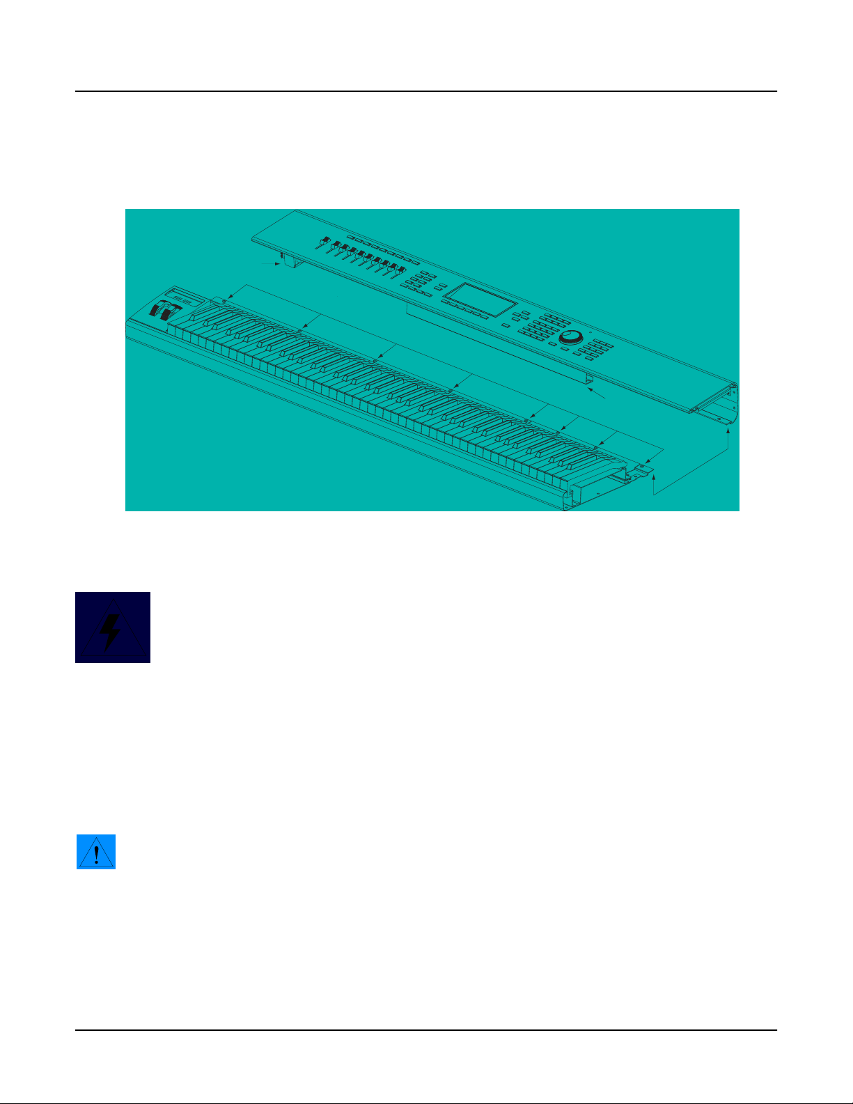
Opening the PC3x
PC3x Bottom
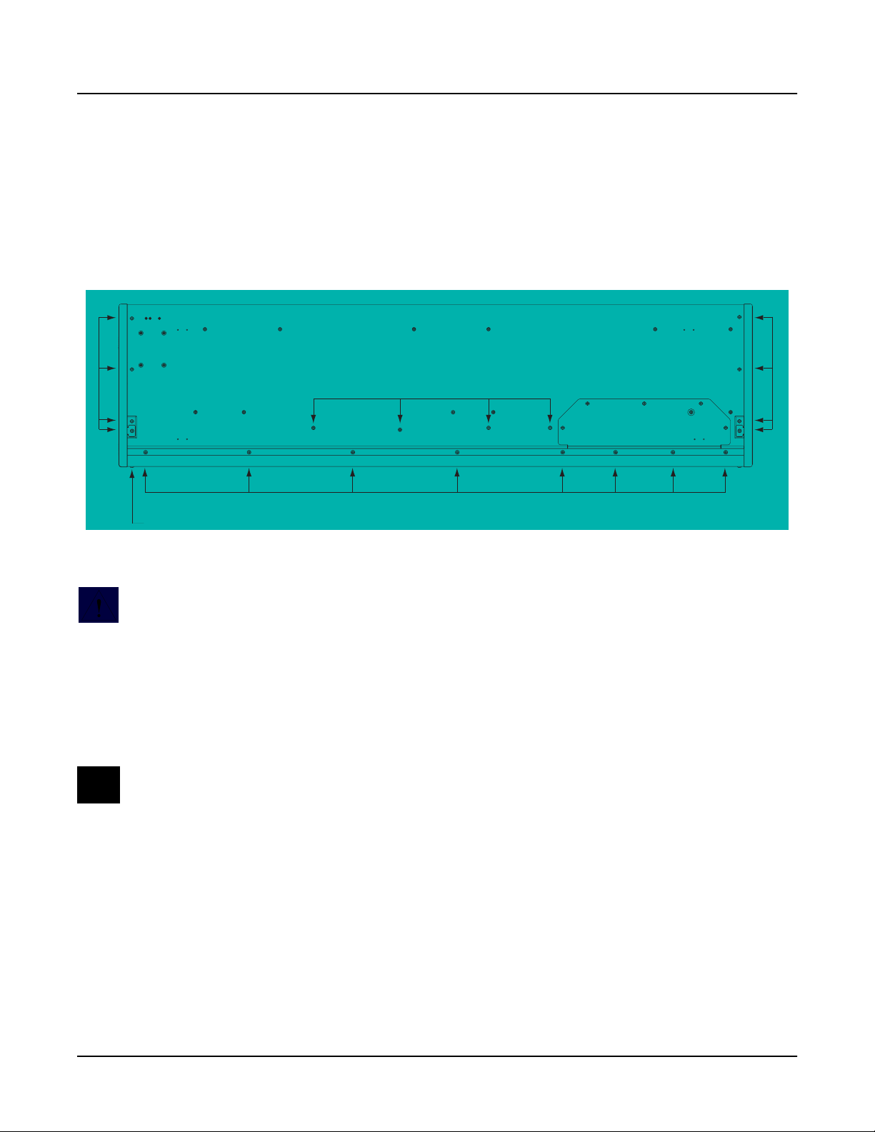
Refer to Figure 3-1. Arrows indicate the locations of the enclosure support wall, endcap and rear
panel screws.
Keyboard
Endcap screws
Enclosure support wall screws
Access panel
*
Rear panel screws
Rear panel
*Endcap locking bracket screws
Endcap screws
*
Figure 3-1 PC3x bottom enclosure
Caution: Do not remove the endcap or rear panel screws at this point of the procedure.
1. Tilt the PC3x up and remove the four enclosure support wall screws.
2. Place the unit flat on your work surface.
3. Move the unit so that the rear panel portion of the unit hangs over the edge of your work
surface. This gives you access to the eight screws that secure the rear panel portion of the
top enclosure to the bottom enclosure. Remove the eight screws.
Note: Two of these screws also secure the rear panel portion of the access panel. It is not
necessary to remove the five remaining access panel screws.
3-2
4. Slide the unit back onto the work surface.
Page 27
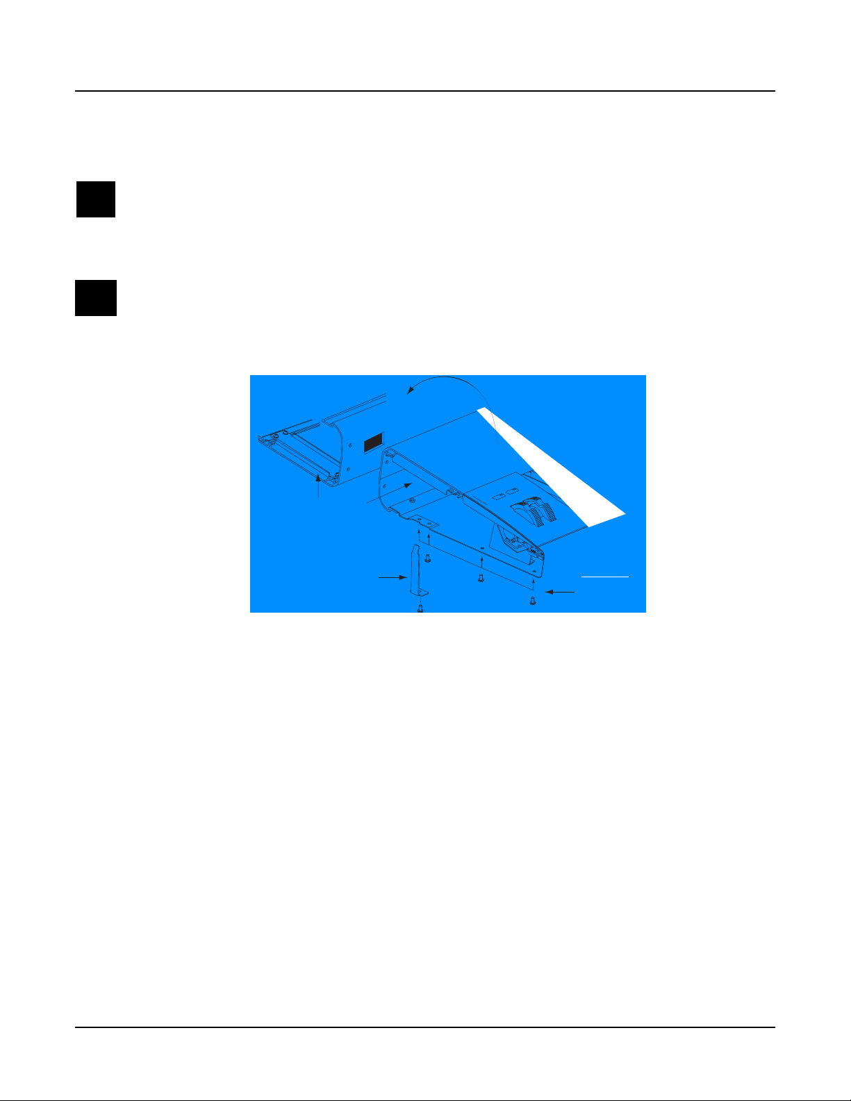
Removing the Top Enclosure
The following procedure assumes that you have completed Steps 1–4 in PC3x Bottom.
Removing the top enclosure requires removing the left and right endcaps. Each endcap includes
the endcap, endcap side bracket and endcap locking bracket.
Endcap
Endcap Side Bracket
Endcap Locking Bracket
Figure 3-2 Endcap assembly
Disassembly/Assembly
Opening the PC3x
1. Refer to Figure 3-3.
2. Remove the four screws that secure the endcaps to the rear panel.
Endcap screws
Endcap screws
Figure 3-3 PC3x rear panel
3. Refer to Figure 3-1. Move the unit so that one end hangs over the edge of your work
surface.
4. Remove the endcap locking bracket screw from the bottom enclosure.
Caution: When you remove the endcap locking bracket screw, the endcap locking bracket may
remain loosely in the endcap. However, it can come out of the endcap. When you remove the
screw securing the endcap locking bracket, hold it in position so that it does not fall out of the
endcap and become lost or damaged.
5. Remove the remaining three screws and set the endcap safely aside.
6. Repeat for the other endcap.
3-3
Page 28
Disassembly/Assembly
Opening the PC3x
7. Refer to Figure 3-4. The bottom edge of the rear panel and back edge of the bottom
enclosure connect to form a lip. The rear panel screws secure the lip.
Transformer
Rear panel screw locations
Enclosure
Support Wall
Lip
Figure 3-4 Top and bottom enclosures
Warning: Be sure to have your work surface prepared. This includes
placing foam blocks behind the unit. When the top enclosure is removed,
place it on the foam blocks to avoid damaging the Alpha Wheel, control
panel buttons, and sliders. The following procedure requires enough room
behind the rear of the unit to place the top enclosure face down on your
work surface.
8. Grip each end of the top enclosure and rotate it back approximately two inches. This
separates the bottom edges of the top enclosure and bottom enclosure.
9. Lift the top enclosure straight up.
10. Turn the top enclosure over and place it face down onto your work surface.
Caution: Table 3-1 lists the cables, by board location, from the top enclosure to the assembly
they connect to on the bottom enclosure. You do not need to disconnect these cables.
3-4
Page 29
Top cover Assembly Bottom Enclosure
Connector Board, Bass Keyboard Assembly, Bass
Connector Board, Treble Keyboard Assembly, Treble
Slider Board Button Board/Wheels Assembly
Connector Board Wheels Assembly
Table 3-1 Top and bottom enclosure cables
Replacing the Top Enclosure
1. Position the top enclosure behind the bottom enclosure.
2. Move the top enclosure so that the bottom edge of the rear panel is positioned under the
bottom enclosure edge. See Figure 3-4 on page 3-4.
Note: Verify that the cables listed in Table 3-1 are lying flat on the bottom enclosure. Be sure that
all other cables are tucked between the top enclosure and the enclosure support wall.
Disassembly/Assembly
Opening the PC3x
3. Hold the top enclosure safely in place and move the unit so that one end of the rear panel
edge hangs over the edge of your work surface and install the rear panel screw at that end.
Slide the unit back onto your work surface. Repeat for other end.
Warning: Perform Steps 3 and 4 separately. Combining these steps could cause the top
enclosure to flip away from the bottom enclosure or drop off of your work surface.
4. Move the unit so that the rear panel edge of the unit hangs over the edge of your work
surface and install the remaining screws.
3-5
Page 30
Disassembly/Assembly
s
Opening the PC3x
Closing the PC3x
Warning: The following procedure assumes that you have completed Steps 3 and 4 in Replacing
the Top Enclosure. If you have not completed these steps, do so before continuing.
1. Refer to Figure 3-1. Tilt the unit up and install the four enclosure support wall screws.
Note: In addition to the rear panel screws, the endcap locking bracket secures the endcap to the
top enclosure. When the endcap locking bracket is in position, it rests against the endcap
clamping bracket located on the underside of the top enclosure. See Figure 3-5.
Endcap Clamping Bracket
Endcap Locking Bracket
Endcap Screw
Figure 3-5 Top enclosure, endcap locking and clamping brackets
2. Slide one side of the unit off of your work surface and hold the appropriate endcap and
endcap locking bracket in position.
3. Install the endcap locking bracket screw in the bottom enclosure.
4. Install the three remaining endcap screws in the bottom enclosure.
5. Repeat for the other endcap.
6. Refer to Figure 3-3. Install the four endcap screws in the rear panel.
3-6
Page 31

Top Enclosure
The top enclosure includes six boards: Connector, Front Panel, LCD, Slider, Engine, and
USB/xD Daughtercard. The enclosure support wall, transformer and AC recptacle are also
included on the top enclosure. Figure 3-6 shows the placement of the enclosure support wall on
the top enclosure. Figure 3-7 shows the placement of the boards, transformer, and AC recptacle
with the enclosure support wall removed.
Disassembly/Assembly
Top Enclosure
USB
Engine Board
Figure 3-6 Top enclosure, enclosure support wall location
Enclosure
Support Wall
Front Panel
LCD
Connector Board
Slider Board
Transformer
Figure 3-7 Top enclosure, board locations, transformer, and AC recptacle
3-7
Page 32

Disassembly/Assembly
Top Enclosure
Removing the Enclosure Support Wall
The shielded cable bundle connecting J302 on the Connector Board to J18 on the Engine Board is
routed and taped along the front of the enclosure support wall. Tape also secures the cable
bundle to the Slider and Front Panel Boards. Always peel back the tape from one side so that the
tape remains properly positioned.
Note: The routing of this cable is important to minimize noise and hum. Be sure to note the
placement of the cable so that you position it properly when you reinstall the enclosure support
wall.
1. Peel back the tape from one side to free the cable bundle from the enclosure support wall
and the Slider Board.
2. Disconnect the cable bundle from J302 on the Connector Board and move the cable bundle
away from the enclosure support wall.
3. Remove the seven screws that secure the enclosure support wall to the top enclosure, and
remove the enclosure support wall.
Replacing the Enclosure Support Wall
1. Align the center screw holes of the three-hole groupings in the enclosure support wall
with the thread marks in the extrusion.
2. Install the seven screws that secure the enclosure support wall to the top enclosure.
3. Secure the cable bundle to the front of the enclosure support wall with the tape.
4. Connect the shielded cable bundle to J302 on the Connector Board and secure it to the
Slider Board with the tape.
Note: The routing of this cable is important to minimize noise and hum. Be sure to note the
placement of the cable so that you position it properly when you reinstall the enclosure support
wall.
3-8
Page 33

Removing the Connector Board
1. Follow the procedure described on page 3-8 to remove the enclosure support wall.
2. Following Steps 3–5, disconnect the cables listed in Table 3-2.
Ref. Name Cable Type Destination
J301 PC3 Power stranded wire Engine Board
J303 MIDI/CPU stranded wire Engine Board
J304 Front Panel flat ribbon Front Panel Board
J305 Slider stranded wire Slider Board
J306 Treble flat ribbon Keyboard Assembly
J307 Bass flat ribbon Keyboard Assembly
J308 Wheels stranded wire Wheels Assembly
J324 AC power stranded wire Transformer
J325 Digital Audio Out stranded wire Engine Board
Table 3-2 Connector Board cables
Disassembly/Assembly
Top Enclosure
3. Disconnect the stranded wire cables from J301, J303, and J325 on the Connector Board.
Note: The cables used throughout the PC3x are bundled and routed so that their locations and
destinations seem obvious. However, to avoid reversing the Bass and Treble cables when
reconnecting, mark one or both cables designating B for Bass and T for Treble.
4. Disconnect the flat ribbon cables from J304, J306, and J307.
Connector Board
AC Power
J301
PC3 Power
Figure 3-8 Cable locations
5. Disconnect the stranded wire cables from J305, J308, and J324.
Dig.
Audio Out
MIDI & CPU
J303 J305
Slider Wheels
J308J325J324
Treble
J306
Bass Front Panel
J307
J304
Audio Out
J302
3-9
Page 34

Disassembly/Assembly
Top Enclosure
*
*
*
longer screws with spacers
Figure 3-9 Rear panel hardware locations
6. Remove the eight screws that secure the Connector Board to the rear panel. Two screws
are longer than the others and have spacers located between the screw and the rear panel.
See Figure 3-9 for the locations of the screws and spacers.
Note: Do not remove any other hardware from this portion of the rear panel.
7. Remove the Connector Board.
Replacing the Connector Board
Refer to Figure 3-10. The Connector Board is designed to work with a number of different
keyboards. This is determined by the position of a diode(s) on the Connector Board. There are
four diode locations, D19 through D22, located between J306 and J307 on the Connector Board.
If you are replacing the Connector Board with a new one, determine the location of the diode(s)
and be sure the new board matches the board you are removing.
3-10
Treble
J306
D19
OPT 1
D21
OPT 2
D20OPT 3
D22
OPT 4
Bass
J307
Figure 3-10 Connector Board, diode configuration
1. Hold the Connector Board and position it so that the rear panel jacks, potentiometers, and
switches are correctly positioned through the rear panel portion of the top enclosure.
2. Install the eight screws that secure the Connector Board to the rear panel. Be sure to place
a spacer and use one of the longer screws at the locations noted in Figure 3-9.
Page 35

Disassembly/Assembly
Top Enclosure
3. Connect the stranded wire cable from the Slider Board to J305 on the Connector Board.
4. Connect the stranded wire cable from the Transformer to J324 on the Connector Board.
5. Connect the stranded wire cable from the Wheels Assembly to J308.
6. Connect the flat ribbon cables from the Keyboard Assembly to J306 and J307 on the
Connector Board.
7. Connect the flat ribbon cable from the Front Panel Board to J304 on the Connector Board.
Warning: If you are replacing the Connector Board with a new board, check the flat ribbon cable
at location J202 on the Front Panel Board. Some earlier units have a small PC board attached to
the flat ribbon cable. If the unit has this small PC Board, check the value of RN10 and RN12 on
the new Connector Board. If a 6.8K resistor network is installed in RN10 and RN12, disconnect
the flat ribbon cable from J202, remove the small PC Board, and reconnect the cable directly to
the Front Panel Board.
8. Connect the stranded wire cables from the Engine Board to J301, J303, and J325 on the
Connector Board.
9. Follow the procedure on page 3-8 to install the enclosure support wall.
Removing the Slider Board
1. Follow the procedure described on page 3-8 to remove the enclosure support wall.
2. Follow the procedure described on page 3-9 to remove the Connector Board.
3. Tilt the top enclosure up and remove the ten slider knobs, then lay it flat on your work
surface.
4. Following Steps 5 and 6, disconnect the cables listed in Table 3-3.
Ref. Name Cable Type Destination
J303 Slider Bridge flat ribbon Front Panel Board
J304 IBBB stranded wire Button Board/Wheels Assembly
Table 3-3 Slider Board cables
5. Disconnect the flat ribbon cable from J303.
6. Disconnect the shielded wire cable from J304.
Note: The stranded wire cable connected to location J302 was disconnected following the
procedure to remove the Connector Board. It is not necessary to disconnect it from the Slider
Board. However, if you are replacing the Slider Board with a replacement board, be sure to
disconnect the cable and connect it to the replacement board.
7. Remove the four screws that secure the front panel edge of the Slider Board.
3-11
Page 36

Disassembly/Assembly
Top Enclosure
8. Remove the four screws that secure the two PC board clamps (two screws per clamp).
9. Remove the Slider Board.
1
J303
FP Bridge
Slider
Board
Figure 3-11 Slider Board, screw locations
These screws also secure the rear panel edge of the Board.
J304
J302
Caution: Each switch button cap uses a set of small pegs to mount the cap to a board. The
button caps on the Slider Board are mounted individually. If a cap becomes separated from the
board, be careful that a peg is not inadvertently broken.
Replacing the Slider Board
1. Position the Slider Board onto the top enclosure.
2. Raise the top enclosure up to verify that the switch button caps and slider shafts are
correctly positioned through their openings in the top enclosure.
3. Align the center screw hole on the front panel edge with the thread marks in the extrusion
and install the four screws that secure the front panel edge.
4. Place a PC board clamp in position. Align the center screw holes of the clamp with the
thread marks in the extrusion and install the two screws that secure the clamp. Repeat for
the other clamp.
5. Tilt the top enclosure up and install the ten slider knobs, then lay it flat on your work
surface.
Caution: To avoid damaging a slider, move the slider shaft to either the top or bottom end of its
travel to install a knob.
6. Connect the stranded wire cable from the Button Board on the Wheels Assembly to J304
on the Slider Board.
3-12
7. Connect the flat ribbon cable from the Front Panel Board to J303 on the Slider Board.
8. If you have disconnected the cable from J302, reconnect it.
9. Follow the procedure on page 3-10 to install the Connector Board.
10. Follow the procedure on page 3-8 to install the enclosure support wall.
Page 37

Removing the LCD Board
1. Follow the procedure described on page 3-8 to remove the enclosure support wall.
2. Follow the procedure described on page 3-9 to remove the Connector Board.
3. Disconnect the flat ribbon cable from J15 on the Engine Board. This cable is bundled with
other cables routed along the rear panel portion of the top enclosure. They are secured
with tie wraps to cable mounts. Removing the LCD requires cutting the tie wraps and
separating the flat ribbon cable from the other cables routed along the rear panel.
4. The LCD is mounted onto a bezel that is secured to the Front Panel Board. Remove the
four screws that secure the LCD to the front panel bezel.
Disassembly/Assembly
Top Enclosure
LCD
J203-2 RETURN BLACK
J203-1 HOT BLUE
Figure 3-12 J203-1 and J203-2 connections on Front Panel Board
5. Refer to Figure 5. A two-wire soldered cable connects the LCD to J203-1 and J203-2 on the
Front Panel Board. These cables are not labeled at the Factory and the colors of the wires
attached to the LCD may vary. Polarity is important! Before you desolder the wires, mark
one of them with a designation such as a black line to avoid reversing the wires when they
are resoldered.
Caution: 1000V high frequency voltage present, which can cause burns–be sure power is off!
6. Desolder the wire connections at J203-1 and J203-2 on the Front Panel Board. Lift the LCD
Board up and remove it.
3-13
Page 38

Disassembly/Assembly
Top Enclosure
Replacing the LCD Board
1. Place the LCD Board in position face down onto the front panel bezel.
2. Install the four screws that secure it to the front panel bezel.
3. Connect the flat ribbon cable to J15 on the Engine Board. Be sure that you bundle the LCD
cable with the other cables positioned along the rear panel and tie wrap them to the cable
mounts.
Caution: 1000V high frequency voltage present, which can cause burns–be sure power is off!
Note: If you are replacing the LCD with a new one and the wire colors are different from the
original, try to match the wires based on how each wire enters the LCD module.
4. Solder the connections at J203-1 and J203-2 on the Front Panel Board. Polarity is
important! If the LCD displays low light, the wires are reversed.
Removing the Front Panel Board
1. Follow the procedure described on page 3-8 to remove the enclosure support wall.
2. Follow the procedure described on page 3-9 to remove the Connector Board.
3. Table 3-4 lists the cables connected to the Front Panel Board.
Note: If the service you are performing only requires that you have access to the Front Panel
Board for component testing or component replacement, it is not necessary to separate the LCD
Board from Front Panel Board.
Ref. Name Cable Type Destination
J201 FP Bridge flat ribbon Slider Board
J202 Front Panel flat ribbon Connector Board
J203 Backlight two-wire cable LCD
Table 3-4 Front Panel Board cables
Note: The flat ribbon cable at location J202 was disconnected following the procedure to remove
the Connector Board. It is not necessary to disconnect it from the Front Panel Board. However, if
you are replacing the Front Panel Board with a replacement board, be sure to disconnect the
cable and connect it to the replacement board.
Warning: If the flat ribbon cable at location J202 has a small PC board connecting it to the Front
Panel Board, you should disconnect it from the Front Panel Board so that it is not damaged
during component testing or replacement. If connector is offset by one pin either way, the Front
Panel Board will be damaged!
3-14
4. Disconnect the flat ribbon cable at J201 on the Front Panel Board.
Page 39

Disassembly/Assembly
Top Enclosure
Note: If the service you are performing only requires that you have access to the Front Panel
Board for component testing or component replacement, it is not necessary to separate the LCD
Board from Front Panel Board.
5. If you are replacing the Front Panel Board with another board, follow the procedure
described on page 3-13 to remove the LCD Board.
Note: If you are replacing the Front Panel Board with another board, be sure to remove the four
screws that secure the LCD bezel to the board and install it on the new board.
6. Seven of the screws that secure the enclosure support wall also secure the front panel edge
of the Front Panel Board. You have already removed the enclosure support wall, but one
screw remains securing this edge of the board. See Figure 3-13, and remove the remaining
screw.
7. Remove the six screws that secure the three PC board clamps (two screws per clamp).
These screws also secure the rear panel edge of the Front Panel Board.
8. Lift the Front Panel Board up from the top enclosure. The spinknob and switch button
caps should remain in place.
Caution: Each switch button cap uses a set of small pegs to mount the cap to the Front Panel
Board. The button caps are mounted individually or in clusters. If a cap becomes separated from
the board, be careful that a peg is not inadvertently broken.
1
J202
Front Panel
LCD
FP Bridge
1
J201
Board
J203-2 RETURN BLACK
J203-1 HOT BLUE
Enclosure Support Wall screw locations
remaining screw
Figure 3-13 Front Panel Board, screw locations
3-15
Page 40

Disassembly/Assembly
Top Enclosure
Replacing the Front Panel Board
Note: If you are replacing the Front Panel Board with another board, be sure to remove the four
screws that secure the LCD bezel to the board and install it on the new board.
1. Position the Front Panel Board onto the top enclosure, then raise the top enclosure up
slightly to verify that the spinknob and switch button caps are correctly positioned
through their openings in the top enclosure.
2. Place a PC board clamp in position. Align the center screw holes of the clamp with the
thread marks in the extrusion and install the two screws that secure the clamp. Repeat for
the other two clamps.
3. Install the screw that secures the front panel edge. See Figure 3-13.
4. If you removed the LCD Board, follow the procedure described on page 3-14 to replace it.
5. Connect the flat ribbon cable from the Slider Board to J201.
6. If you have disconnected the cable from J202, reconnect it.
Warning: If this cable has a small PC board, be very careful to plug the small PC board onto all
of the pins of J202. If it is offset by one pin either way, the Front Panel Board will be damaged!
7. Follow the procedure on page 3-10 to install the Connector Board.
8. Follow the procedure on page 3-8 to install the enclosure support wall.
3-16
Page 41

Removing the Engine Board
The USB/xD Daughtercard is mounted on the Engine Board. The following procedure describes
removing the Engine Board with the USB/xD Daughtercard attached.
1. Following Steps 2–4, disconnect the cables listed in Table 3-5.
Ref. Name Cable Type Destination
J5 MIDI & CPU stranded wire Connector Board
J15 Graphic LCD flat ribbon LCD Board
J18 PC3 Audio Out shielded wire Connector Board
J21 PC3 Power stranded wire Connector Board
J33 Digital Audio Out stranded wire Connector Board
Table 3-5 Engine Board cables
2. Disconnect the shielded wire cable from J18.
3. Disconnect the stranded wire cables from J5, J21, and J33.
Disassembly/Assembly
Top Enclosure
4. Disconnect the flat ribbon cable from J15.
5. Remove the two screws that secure the USB/xD Daughtercard to the rear panel.
6. Remove the three screws that secure the front panel edge of the Engine Board.
J12
USB/SM
Card
on Engine
Board
USB/xD
Daughter Card
J1
Dig. Audio Out
J20
J18
Audio
Out
Battery
J5
Bank 1
Bank 0
J33
Graphic LCD
MIDI & CPU
J15
J10
J21
PC3 Power
Expansion Sound ROMJ11
Expansion Sound ROM
Engine Board
Figure 3-14 Engine Board, screw locations
7. Remove the two screws that secure the PC board clamp and rear panel edge of the Engine
Board to the top enclosure.
8. Remove the Engine Board.
3-17
Page 42

Disassembly/Assembly
Top Enclosure
Replacing the Engine Board
1. Place the Engine Board in position on the top enclosure.
Note: Be sure the blue xD Daughtercard bezel is seated in the rear panel cutout properly.
2. Align the center screw hole on the front panel edge with the thread marks in the extrusion
and install the three screws that secure the front panel edge. See Figure 3-14.
3. Install the two screws that secure the USB/xD Daughtercard to the rear panel.
4. Connect the flat ribbon cable from the LCD to J15 on the Engine Board.
5. Connect the stranded wire cables from the Connector Board to J5, J21, and J33 on the
Engine Board.
6. Connect the shielded wire cable from the Connector Board to J18 on the Engine Board.
Removing the USB/xD Daughtercard
The USB/xD Daughtercard is mounted on the Engine Board and is held in place with a 28-pin
connector.
1. Follow the procedure described on page 3-17 to remove the Engine Board.
2. Lift the USB/xD Daughtercard straight up to disconnect it from J12 on the Engine Board.
Replacing the USB/xD Daughtercard
1. Position the USB/xD Daughtercard over the 28-pin connector at J12 on the Engine Board.
2. Verify that the Engine Board pins are lined up properly with the 28-pin connector on the
USB/xD Daughtercard. Press the USB/xD Daughtercard down to insert the pins into the
28-pin connector.
3. Follow the procedure described on page 3-18 to install the Engine Board.
3-18
Page 43

Removing the Wheels Assembly
1. Refer to Figure 3-15 on page 3-20. Slide the left side of the unit forward off of your work
surface so that you can access the four screws and washers securing the assembly to the
bottom enclosure. Remove the four screws and washers.
2. Slide the unit back onto your work surface.
3. Lift the Wheels Assembly up, approximately two inches. Nylon reinforced tape secures
the Aftertouch flex cables to the bottom enclosure. Peel back the tape from one side and
disconnect the cables, J202 to the keyboard front pressure (white key) and J203 to the
keyboard back pressure (black key).
4. Disconnect the stranded wire cable from J201 on the Wheels Board.
5. Disconnect the stranded wire cable from J304 on the Slider Board.
6. Remove the Wheels Assembly.
Replacing the Wheels Assembly
1. Hold the Wheels Assembly in position over the bottom enclosure.
2. Connect the stranded wire cable from the IBBB Board to J304 on the Slider Board.
Disassembly/Assembly
Top Enclosure
3. Connect the stranded wire cable from the Connector Board to J201 on the Wheels Board.
4. Connect the flat flex cables, J202 from the keyboard front pressure (white key) and J203
from the keyboard back pressure (black key).
5. Reapply the nylon reinforced tape to the flat flex cables.
6. Lower the Wheels Assembly into position.
7. Slide the unit forward and install the four screws and washers to secure the Wheels
Assembly to the bottom enclosure.
3-19
Page 44

Disassembly/Assembly
PC3x Keyboard Assembly
PC3x Keyboard Assembly
Removing the PC3x Keyboard Assembly
The following procedure assumes that the PC3x is open and that you have followed the
instructions to remove the top enclosure.
1. The keyboard is secured to the bottom enclosure using twelve screws. Refer to Figure 3-15
for the position of the screws. Arrows identify the locations of the twelve screws.
2. Tilt the PC3x up and remove the six keyboard rear screws, then lay the PC3x flat on your
work surface.
3. Move the PC3x forward so that the front hangs over the edge of your work surface to
access the remaining screws, and remove the six keyboard front screws.
4. Slide the PC3x back onto your work surface.
5. Slide the left side of the unit forward off of your work surface so that you can access the
four screws and washers securing the Wheels Assembly to the bottom enclosure. Remove
the four screws and washers.
Keyboard
Wheels Assembly screws
6. Slide the PC3x back onto your work surface.
7. At this point the keyboard is loose in the bottom enclosure, but it has cables connected to
8. Lift the Wheels Assembly and disconnect the Aftertouch flex cables. These cables have
9. Place the Wheels Assembly in its position on the bottom enclosure.
Keyboard front screws
Keyboard rear screws
Access panel
Rear panel
Figure 3-15 PC3x keyboard bottom
the Wheels Assembly and the Connector Board.
nylon reinforced tape securing them to the bottom enclosure. Peel back the tape from one
side to free the cables.
3-20
10. Disconnect the flat ribbon cables from locations J306 and J307 on the Connector Board.
These cables are also secured to the bottom enclosure with nylon reinforced tape. Peel
back the tape from one side to free the cables.
Page 45

Note: If you need access to the keyboard to replace one or more keys, it is not necessary to
entirely remove the Keyboard Assembly from the PC3x. Follow the procedure on page 3-22.
11. Remove the Keyboard Assembly.
Replacing the PC3x Keyboard Assembly
1. Place the keyboard on the bottom enclosure. Be sure that the flat ribbon cables from the
keyboard are correctly positioned to connect them to the Connector Board.
Note: If you have disconnected the Bass and Treble ends of the flat ribbon cables from the
keyboard contact boards during service, be sure that you have reconnected them and secured
them with tape. Be sure that the small ribbon cable connecting the Bass and Treble Contact
Boards is connected.
2. Connect the flat ribbon cables to J306 and J307 on the Connector Board.
3. Secure the flat ribbon cables to the bottom enclosure. Be sure to reapply the nylon
reinforced tape that secures the cables to the bottom enclosure.
Disassembly/Assembly
PC3x Keyboard Assembly
4. Lift the Wheels Assembly and connect the Aftertouch flex cables. Be sure to reapply the
nylon reinforced tape that secures the flex cables to the bottom enclosure.
5. Slide the left side of the unit forward and install the four screws and washers to secure the
Wheels Assembly to the bottom enclosure.
6. Move the PC3x back onto your work surface.
7. Slide the PC3x forward so that you can install the six keyboard front screws.
8. Move the PC3x back onto your work surface.
9. Tilt the PC3x up and install the six keyboard rear screws.
3-21
Page 46

Disassembly/Assembly
PC3x Keyboard Assembly
Removing Keys
The following procedure assumes you have removed the top enclosure from the PC3x.
1. Follow the procedure to remove the keyboard.
Note: If you are merely replacing one or more keys, it is not necessary to entirely remove the
keyboard from the PC3x. Once you have followed the procedure to remove the keyboard, you
can slide it toward the rear panel to give you enough access to remove and replace keys.
2. The following diagrams illustrate the outlines of the natural and sharp keys and the
Natural/White Key
Pivot
location
location and functions of the components described in the following procedures.
Key Spring
location
Strikes the front and rear key
contact on key depression
Figure 3-16 Natural/white key
Pivot
location
Key Spring
location
Strikes the front and rear key
contact on key depression
Figure 3-17 Sharp/black key
Hooks under the front
of the keyboard chassis
Hooks through
the keyboard chassis
3-22
Page 47

Removing Natural/White Keys
1. Unlock the key from the pivot anchoring the key to the keyboard chassis. To do this, insert
a small flat screwdriver at the back end of the pivot and press toward the front edge of the
keyboard. While doing so, lift the back end of the key.
2. Remove the screwdriver.
3. The key should now be free of the pivot. Lift the key up slightly, then forward. The front
edge of each key hooks under the keyboard chassis. Be sure the key is not hooked under
the keyboard chassis prior to lifting the key off.
Caution: Each key has a small key spring. The key spring is positioned on the keyboard chassis
(just in front of the pivot) and is held in place when the key is installed. When you remove a key,
be sure you do not misplace the key spring.
Removing Sharp/Black Keys
1. To remove a sharp key, first remove the adjacent natural keys, as described in the previous
procedure.
2. Unlock the key from the pivot anchoring the key to the keyboard chassis. To do this, insert
a small flat screwdriver at the bottom of the pivot and press toward the front edge of the
keyboard. While doing so, lift the back end of the key.
Disassembly/Assembly
PC3x Keyboard Assembly
3. Remove the screwdriver.
4. The key should now be free of the pivot. Lift the back of the key up slightly, then forward.
The front edge of each key hooks through the keyboard chassis. Once the key is free of the
pivot, you should be able to lift the key out from the keyboard chassis.
Caution: Each key has a small key spring. The key spring is positioned on the keyboard chassis
(just in front of the pivot) and is held in place when the key is installed. When you remove a key,
be sure you do not misplace the key spring.
Replacing a Sharp Key
Note: Always replace a sharp key before replacing the adjacent natural keys.
1. Verify the placement of the key spring.
2. Position the front end of the key through the keyboard chassis.
3. Lower the key into position. Align the pivot with the hole at the rear of the key.
4. Push down on the key. It should snap into position onto the pivot.
3-23
Page 48

Disassembly/Assembly
PC3x Keyboard Assembly
Replacing a Natural/White Key
1. Verify the placement of the key spring.
2. Hook the front end of the key under the keyboard chassis.
3. Lower the key into position. Align the pivot with the hole at the rear of the key.
4. Push down on the key. It should snap into position onto the pivot.
Servicing the Keyboard Contact Boards
The Keyboard Assembly has nine keyboard stiffening brackets positioned along the underside
of the chassis. Each bracket is secured to the keyboard chassis using three screws: two small
machine screws through the chassis and one black screw through the contact board. To remove a
contact board, you must first remove the stiffening brackets.
1. Tilt the keyboard up (front edge of the keys facing down), and disconnect the flat ribbon
cables that connect the Treble and Bass Contact Boards to the Connector Board. The
connectors are secured with tape. Peel back the tape to free the cables. Set the cables safely
aside and lower the keyboard.
2. Place the keyboard upside down on a flat soft surface. Be sure that the keys are resting on
a soft surface to avoid scratching or other damage. The stiffening brackets and Treble and
Bass Contact Boards are now visible.
Removing the Treble Contact Board
1. Disconnect the small ribbon cable that connects the Treble and Bass Contact Boards.
2. Remove the five stiffening brackets. Remove the 15 screws that secure the five brackets.
3. Remove the remaining 18 screws that secure the Treble Contact Board to the keyboard
chassis, and remove the Treble Contact Board.
Replacing the Treble Contact Board
1. Position the Treble Contact Board on the keyboard chassis. Be sure that the rubber key
contacts line up properly through the holes in the keyboard chassis.
2. Install the 18 screws that secure the board to the keyboard chassis.
3. Connect the small ribbon cable that connects the Treble to the Bass Contact Board.
4. Install the five stiffening brackets. Install the 15 screws that secure the five brackets.
Removing the Bass Contact Board
1. Disconnect the small ribbon cable that connects the Bass and Treble Contact Boards.
2. Remove the four stiffening brackets. Remove the 12 screws that secure the four brackets.
3. Remove the 18 screws that secure the board to the keyboard chassis, and remove the Bass
Contact Board.
3-24
Page 49

Replacing the Bass Contact Board
1. Position the Bass Contact Board on the keyboard chassis. Be sure that the rubber key
contacts line up properly through the holes in the keyboard chassis.
2. Install the 18 screws that secure the board to the keyboard chassis.
3. Connect the small ribbon cable that connects the Bass to the Treble Contact Board.
4. Install the four stiffening brackets. Install the 12 screws that secure the brackets.
Connecting the Keyboard Contact Boards
1. Turn the keyboard over to its normal playing position.
2. Tilt the keyboard up (front of the keys facing down), and connect the flat ribbon cables
that connect the Treble and Bass Contact Boards to the Connector Board. Be sure to
reapply the tape to secure the connectors. Lower the keyboard.
Removing the Keyboard Contact Strips
1. Place the keyboard upside down on a flat soft surface. Be sure that the keys are resting on
a soft surface to avoid scratching or other damage.
Disassembly/Assembly
PC3x Keyboard Assembly
2. Follow the procedure to remove the Bass and Treble Keyboard Contact Boards.
3. Examine the keyboard contact strips and look at the design of an individual contact. The
top portion of the contact has two indentations. One indentation is deeper than the other.
When replacing the keyboard contact strips, the deeper indentation is always positioned
toward the rear of the key.
4. The keyboard contact strips have mounting pegs that secure the contact strips to the
keyboard contact boards.
5. To remove a keyboard contact strip, gently lift and free the strip from its position. Be
careful not to rip or damage any contact in the process.
Replacing the Keyboard Contact Strips
1. Position the contact strip on the Keyboard Contact Board that you are servicing.
Note: Be sure that the deeper indentation is positioned toward the rear of the key.
2. Line up the contact strip mounting pegs with their respective mounting holes on the
keyboard contact board.
3. Using a small blunt-end tool (Q-Tip, toothpick, etc.), gently push the mounting pegs
through the holes. Do not use too much force or use a tool that can poke a hole through
the mounting pegs. However, be sure that the mounting pegs are installed through the
holes and the contact strip is flat against the PC board at each peg location.
3-25
Page 50

Disassembly/Assembly
PC3x Keyboard Assembly
3-26
Page 51

Chapter 4
Troubleshooting & Maintenance
Introduction
Cables, Connectors
Cables
All cables with connectors are keyed, and therefore cannot be reversed.
Warning: Some units may have a small PC board installed on the flat ribbon cable connected to
J202 on the Front Panel Board. Neither the socket nor the pins on this board are keyed. See
Removing the Front Panel Board in Chapter 3, page 3-14 and page 3-16 for further information.
Cable Routing
In some cases, tape fastens cables to printed circuit boards or the top and bottom enclosures.
When disconnecting cables, always peel back the tape from one side so that the tape remains
properly positioned.
Surface-Mount Devices
The removal and replacement of surface-mount devices requires training and the proper
equipment. If you do not have the training or equipment to remove or replace surface-mount
devices, contact the service department to order a board replacement. International service
technicians should contact their appropriate Young Chang Distributor.
Required Tools and Materials
• No. 1 Phillips head screwdriver
• No. 2 Phillips head screwdriver
• Small flat head screwdriver
• Dowel (3mm diameter)
• Needle-nose pliers
• Small blunt-end tool (Q-Tip, toothpick, etc.)
• Extraction tool (use only an AMP 822154-1)
• USB cable
• xD card
• Foam blocks
4-1
Page 52

Troubleshooting & Maintenance
Boot Loader
Boot Loader
Use the PC3x’s Boot Loader to enter Diagnostics or perform a Hard Reset to the unit. You can
also install operating system updates and objects into Flash memory.
Entering the Boot Loader
Apply power to the unit. When the ****Welcome to the Kurzweil PC3**** message
appears in the LCD, quickly press and release the Exit button.
There are five menu options available in the PC3x Boot Loader. The following is a brief
description of the available menu options.
Run PC3—Exits the Boot Loader and returns the unit to normal operation.
Update Image—Select this to install new system software and objects.
Run Diags—Enters the diagnostic test menu. For a complete list of tests and the procedure to
execute the diagnostic tests, refer to Chapter 2, Diagnostics.
System Reset—Clears the memory and restores the unit to factory default settings.
File Utilities—Use this to select one of the following functions: format an xD card, save and
restore PC3x files, or execute a PC3x image from an xD card or USB file.
Resets
Hard Reset
Soft Reset
There are two ways to perform a Hard Reset to the PC3x.
1. Press the Master Mode button. On page 1 in Master Mode, press the soft button below
Reset. The LCD displays a warning message indicating all user objects will be deleted.
Press the soft button below Yes to erase all user objects and restore the unit to factory
settings or the soft button below Cancel.
2. Enter the Boot Loader and press the soft button below System Reset. The LCD displays
a warning message that all user objects will be deleted. Press the soft button below Reset
to erase all user objects and restore the unit to factory settings or the soft button below
Cancel.
The Soft Reset does not erase user programs and setups and is equivalent to turning the power
off and on. To Soft Reset a PC3x, simultaneously press the +/-, 0 and Clear buttons.
4-2
Page 53

Saving User Data
To save user data, first apply power to the PC3x. Once the unit is on and ready for normal
operation, follow the procedure to save user data to an xD card or a computer.
Saving to an xD Card
Note: The following procedure assumes that you have a computer with an xD card writer. Use
either a Windows or MacOS formatted xD card up to 256 Mb. If you format an xD card, use DOS
format, FAT 16.
You can format xD cards on the PC3x, enter the Boot Loader and select the FILE UTILITIES
soft button. However, the maximum size for xD cards formatted on the PC3x is 128Mb.
1. Insert a formatted xD card into the card slot located on the rear panel of the PC3x.
2. Press the Storage Mode button.
3. The card should be the currently selected storage device.
4. Press the Store soft button.
Troubleshooting & Maintenance
Saving User Data
5. Highlight All Types and press the Select soft button. (An asterisk to the left of the file
name indicates the selected file.) Use the Right or Left cursor buttons to highlight
Range/Bank and turn the Alpha Wheel to scroll down to Everything. Press the
Select soft button.
6. Press the Store soft button.
7. Press the OK soft button and follow the display prompts.
Saving to a Computer
1. Connect a USB cable from a computer to the USB port on the PC3x.
2. Press the Storage Mode button.
3. Press the Right or Left cursor buttons or turn the Alpha Wheel to highlight USB
Temporary Drive.
4. Select the Choose soft button. The display indicates that the USB port is changed from a
MIDI to a USB connection.
5. Press the Store soft button.
6. Highlight All Types and press the Select soft button. (An asterisk to the left of the file
name indicates the selected file.) Use the Right or Left cursor buttons to highlight
Range/Bank and turn the Alpha Wheel to scroll down to Everything. Press the
Select soft button.
7. Press the Store soft button.
8. Press the OK soft button and follow the display prompts.
4-3
Page 54

Troubleshooting & Maintenance
Software Updates
Software Updates
Updating with an xD Card
Warning: This procedure requires performing a hard reset. All user objects will be erased. Before
continuing, be sure to save all user programs and setups to an xD card or computer following
the procedure on page 4-3.
The following procedure assumes that you have a computer with an xD card writer. Use either a
Windows or MacOS formatted xD card up to 256 Mb. If you format an xD card, use DOS format,
FAT 16.
You can format xD cards on the PC3x, enter the Boot Loader and select the FILE UTILITIES
soft button. However, the maximum size for xD cards formatted on the PC3x is 128Mb.
1. Go to www.kurzweilmusicsystems.com and follow the links to download the latest
software version.
2. Insert an xD card into the card writer and drag and drop the downloaded files onto the
card.
3. Remove the xD card and insert it into the xD card slot on the PC3x.
4. Apply power to the unit. When the ****Welcome to the Kurzweil PC3****
message appears in the LCD, quickly press and release the Exit button.
5. From the PC3x Boot Loader, select UPDATE IMAGE.
6. Select the MAIN IMAGE soft button.
7. Use the Up or Down cursor buttons or turn the Alpha Wheel to move through the list of
available files. (An asterisk to the left of the file name indicates the selected file.)
Note: Operating System files have .BIN as the file extension. Object files have .PC3 as the file
extension.
8. Press the CHOOSE soft button to begin updating. The LCD displays a message when the
process is complete. Typically, this should take about ten seconds.
9. Press the OK soft button.
10. Select MAIN OBJECT from the UPDATE IMAGE menu.
11. Repeat Steps 7–9.
12. From the Boot Loader main menu, select the SYSTEM RESET button. The LCD displays a
warning message that all user objects will be deleted. Select the soft button below Reset.
4-4
13. Select the RUN PC3 soft button from the main menu to test the software updates.
Page 55

Updating via Computer
Warning: This procedure requires performing a hard reset. All user objects will be erased. Before
continuing, be sure to save all user programs and setups to an xD card or computer following
the procedure on page 4-3.
1. Connect a USB cable from a computer to the USB port on the PC3x.
2. Apply power to the unit. When the ****Welcome to the Kurzweil PC3****
message appears in the LCD, quickly press and release the Exit button.
3. Check the computer desktop and verify that the “Kurzweil PC3”device is present. This
should appear on the desktop as an icon or window. Typically, this should take about 2–3
seconds. However, it can take up to 30 seconds to be recognized.
4. Go to www.kurzweilmusicsystems.com and follow the links to download the latest
software version.
Note: Be sure to always read the downloaded release notes and installation instructions in case
they have changed since this manual was written.
Troubleshooting & Maintenance
Software Updates
5. From the PC3x Boot Loader, select UPDATE IMAGE.
6. Select the MAIN IMAGE soft button.
7. Use the Up or Down cursor buttons or turn the Alpha Wheel to move through the list of
available files. (An asterisk to the left of the file name indicates the selected file.)
Note: Operating System files have .BIN as the file extension. Object files have .PC3 as the file
extension.
8. Press the CHOOSE soft button to begin updating. The LCD displays a message when the
process is complete.
9. Press the OK soft button.
10. Select MAIN OBJECT from the UPDATE IMAGE menu.
11. Repeat Steps 7–9.
12. From the Boot Loader main menu, select the SYSTEM RESET button. The LCD displays a
warning message that all user objects will be deleted. Select the soft button below Reset.
13. Select the RUN PC3 soft button from the main menu to test the software updates.
4-5
Page 56

Troubleshooting & Maintenance
Rebuilding the Internal NAND Flash Memory
Rebuilding the Internal NAND Flash Memory
It is unlikely but possible for the Internal NAND Flash Memory to become corrupted such that
normal hard reset and software update procedures fail. In particular, if the LCD displays the
following: Internal File System Error. Low-level fmt error. and recurs even
after a power cycle, the internal flash memory file system is probably corrupted.
The following procedure can be used to rebuild the Internal NAND Flash Memory using either
an xD card or the USB port via computer. Before starting you will need a special utility program
called PC3FT040.BIN or a later version (last 3 digits are a higher number). This program may be
downloaded from the kurzweilmusicsystems.com website. This program can reformat the
internal flash memory then copy needed system files to it. The Diagnostics file can also be
downloaded from the website.
Rebuilding with an xD Card
Warning: Rebuilding the Internal NAND Flash Memory also does a hard reset erasing all user
created files and restores the unit to factory settings.
The following assumes that you are familiar with the procedures to enter the Boot Loader and
perform normal system updates using an xD Card or the USB port via computer.
1. 1. Using an xD card reader/writer, copy these four files to an xD card:
• File Transfer utility, PC3FT040.BIN or higher
• PC3 Operating System file, PC3OS111.BIN or higher
• PC3 Diagnostics file, PC3DG018 or higher
• PC3 Objects file, PC3OB111.PC3 or higher
2. Turn on the PC3x and enter the Boot Loader. Then insert the xD card into the slot on the
PC3x.
3. Press the File Utilities soft button.
4.
5. Press the EXEC from file soft button.
6. Using the Alpha Wheel, select the File Transfer Utility file then press the CHOOSE soft
button. In a couple of seconds the program will run and display a new menu.
7. Press the FORMAT FLASH soft button. Press the FORMAT soft button again to confirm.
Formatting will take about 5-10 seconds.
8. A new menu should appear. The third line will display, File system not set up.
9. Press the SETUP SYSTEM soft button. A message File structure built will appear
briefly then another menu.
10. The first line should display, Choose a synth executable file:. Use the Alpha
Wheel to select the PC3 Operating System file then press the CHOOSE soft button.
Installation will take about five seconds.
4-6
Page 57

11. The top line should now display, Choose a diags executable file:. Select the
Diagnostics file, then press the CHOOSE soft button. Installation will take only a second or
two. A message Bootable system built. displays briefly then a new menu will
display.
12. The top line should now display, Choose a system objects file:. Select the PC3
Objects file then press the CHOOSE soft button. Installation will take about 10 seconds. A
message System objects installed. displays briefly then the root menu will
display.
13. Press the Quit soft button then press the <back> soft button on the next menu. The
normal Boot Loader menu should now be displayed.
14. Press the RUN PC3 soft button. The PC3x should boot up normally.
Rebuilding via a Computer
Warning: Rebuilding the Internal NAND Flash Memory also does a hard reset erasing all user
created files and restores the unit to factory settings.
Troubleshooting & Maintenance
Rebuilding the Internal NAND Flash Memory
The following assumes that you are familiar with the procedures to enter the Boot Loader and
perform normal system updates using an xD Card or the USB port via computer.
1. Connect a USB cable from a computer to the USB port on the PC3x.
2. Apply power to the unit. When the ****Welcome to the Kurzweil PC3****
message appears in the LCD, quickly press and release the Exit button.
3. Check the computer desktop and verify that the “Kurzweil PC3”device is present. This
should appear on the desktop as an icon or window. Typically, this should take about 2–3
seconds. However, it can take up to 30 seconds to be recognized.
4. Copy the File Transfer utility, PC3FT040.BIN or higher, to the Virtual USB drive.
5. Press the File Utilities soft button.
6. Press the EXEC from file soft button.
7. Using the Alpha Wheel, select the File Transfer Utility file then press the CHOOSE soft
button. In a couple of seconds the program will run and display a new menu.
Note: On Macintosh Operating systems, a message will appear stating that a Device has been
removed. Click the OK (on your Mac) and proceed. On Windows XP Operating systems, the
Virtual USB drive will go away and come back empty. It may take a few seconds for the Virtual
USB drive to appear again. If it does not automatically appear, you can find it by going to My
Computer and it should be under Devices with Removable Storage.
8. At this point, the File Utilities application has already been executed (this is what you are
running), and will no longer appear in the Virtual USB drive. You will need to copy the
following three files to the USB drive on your computer desktop:
4-7
Page 58

Troubleshooting & Maintenance
Rebuilding the Internal NAND Flash Memory
• PC3 Operating System file, PC3OS111.BIN or higher
• PC3 Diagnostics file, PC3DG018 or higher
• PC3 Objects file, PC3OB111.PC3 or higher
9. Press the SETUP SYSTEM soft button. A message File structure built will appear
briefly then another menu.
10. The first line should display, Choose a synth executable file:. Use the Alpha
Wheel to select the PC3 Operating System file then press the CHOOSE soft button.
Installation will take about five seconds.
11. The top line should now display, Choose a diags executable file:. Select the
Diagnostics file, then press the CHOOSE soft button. Installation will take only a second or
two. A message Bootable system built. displays briefly then a new menu will
display.
12. The top line should now display, Choose a system objects file:. Select the PC3
Objects file then press the CHOOSE soft button. Installation will take about 10 seconds. A
message System objects installed. displays briefly then the root menu will
display.
13. Press the Quit soft button then press the <back> soft button on the next menu. The
normal Boot Loader menu should now be displayed.
14. Press the RUN PC3 soft button. The PC3x should boot up normally.
4-8
Page 59

Boot EPROM
The PC3x uses a 32 pin EPROM located at U4 to store the boot up information for the CPU.
Removing the EPROM
1. Place the PC3x upside down on a flat protected surface.
2. Remove the seven screws that secure the access panel and set it safely aside.
3. Use an AMP 822154-1 extraction tool to remove the EPROM.
Warning: Typically, you would insert the tool at one corner to lift the EPROM then repeat the
process at the other corner. However, because of the proximity between the U4 socket and the
keyboard, this is not possible.
4. Insert the thin, straight end of the tool into the extraction hole closest to the xD/Daughter
Board.
5. Slightly, lift up the corner of the EPROM.
Troubleshooting & Maintenance
Boot EPROM
Warning: While the extraction tool is inserted into the extraction hole, do not to allow the tool to
move from side to side. Doing so could cause damage to the EPROM or the socket.
6. Remove the tool.
7. Insert the curved end of the tool into the same extraction hole.
8. To remove the EPROM, slide the tool farther toward the center of the EPROM so that it
will lift straight up and out of the socket.
Caution: Place a finger on top of the EPROM so that it does not pop out suddenly either
damaging it or landing in an inaccessible area.
Replacing the EPROM
1. Position the EPROM over the socket. Be sure the beveled corner of the EPROM is correctly
positioned over the corresponding corner of the socket.
Caution: If you need to reposition the EPROM, always lift it up from the socket first.
2. Gently press the center of the EPROM into the socket and verify that the EPROM is
correctly positioned. Using too much pressure, may cause the PC board to flex and
damage the delicate solder connections under the MARA ICs.
3. Position the access panel on the bottom enclosure and install the seven screws to secure it.
4-9
Page 60

Troubleshooting & Maintenance
Replacing the Battery
Replacing the Battery
The PC3x uses a flat three volt Lithium coincell battery to power the clock. When the battery
voltage runs low, the unit boots up with a low battery message.
Note: The battery voltage can be checked at anytime using the Scanner Diagnostics. See
page 4-11 for more information.
Accessing the Battery
1. Place the PC3x upside down on a flat protected surface.
2. Remove the seven screws that secure the access panel and set it safely aside.
Removing the Battery
The battery (CR2032) in the PC3x keyboard is mounted into a holder on the Engine Board and is
accessible when the access panel is removed.
1. Insert a flat plastic tool (plastic knife, pen cap, etc.) into one of the openings between the
battery and the holder to lift the battery.
Insert the tool here
to lift the battery.
Figure 4-1 Battery and holder
2. Ease the battery out of the holder. If necessary, insert the plastic tool at the bottom of the
holder (closest to the Engine Board) to remove the battery.
Installing the Battery
Caution: Danger of explosion if battery is incorrectly replaced. Replace only with the same or
equivalent type (CR2032).
1. Position the battery over the holder so that the positive terminal is pointing to the
Expansion ROM sockets.
CR2032
Insert the tool between
the holder and the battery
to ease the battery out
of the holder.
4-10
2. Slide the battery into the holder and apply slight pressure until it snaps into place.
3. Position the access panel on the bottom enclosure and install the seven screws to secure it.
Page 61

Scanner Tests
The Scanner Tests for the PC3x include separate tests for the front panel buttons and LEDs, front
panel sliders including the Master Volume slider, the Alpha Wheel, the Mod and Pitch wheels,
the keyboard, and the pedals.
Note: Before beginning the tests, remove the cables from the main output jacks. If a cable is
plugged into the main right output jack when you enter the Scanner Tests, you will see a
RIGHT JACK message in the display.
To enter the Scanner Tests, first turn on the PC3x. Once the PC3x is on and ready to play,
simultaneously hold down the 4, 5 and 6 buttons. All front panel LEDs will flash and the LCD
will slowly display the following:
Troubleshooting & Maintenance
Scanner Tests
PC3 Scan V1.5 DIAG B=3.2 W=122 OPT=-3--
SLIDER 4 = 128
OK
Figure 4-2 LCD example, PC3x scanner tests
The first line of the display shows the scanner software version, the battery voltage, the current
value for the Pitch Wheel position, and the keyboard configuration. The second line shows the
results of the current test. Figure 4-2 shows the result of a slider test—in this case moving
slider 4 to center.
Note: While running the Scanner Tests, the blue Program button LEDs light up in different
patterns. The pattern represents the hexadecimal value of the button.
To exit the Scanner Tests and return to normal operation, simultaneously press the Cancel and
Enter buttons.
Front Panel Buttons
To test a button, press any front panel button. An example of the expected test result for the
Program button follows:
BUTTON 12 Program
The number “12” is the row/column matrix address of the button and Program is the expected
button at that address.
4-11
Page 62

Troubleshooting & Maintenance
Scanner Tests
Alpha Wheel
To test the Alpha Wheel, turn it to increase or decrease the value by one. Turning clockwise
should increase the numbers in order 0-1-2-3-0-1-2... and decrease the numbers in order 3-2-1-03-2-1... turning counterclockwise. The expected test result when the Alpha Wheel is turned is
one of four values–0, 1, 2, or 3:
SPINKNOB = 3
Front Panel Sliders
To test the front panel sliders, move a slider to check its value at the bottom, center, and top. An
example of the normal test results for the Slider A follows (your results may vary slightly):
At bottom: SLIDER 1 = 0
At center: SLIDER 1 = 128
At top: SLIDER 1 = 255
Right Main Output
Insert a 1/4” plug or cable into the Main Right Output. The expected test result follows:
RIGHT JACK
Remove the plug or cable and the message should disappear.
Switch Pedals 1, 2, and 3
To test a switch pedal, press the pedal. An example of the expected test result for the switch
pedal 1 follows:
Full depression: PEDAL 1
Continuous Control Pedal 1 and 2
To test the continuous control pedal, press the pedal. An example of the expected test result for
the continuous control pedal follows:
No depression: CTRL PEDAL = 0
Full depression: CTRL PEDAL = 255
4-12
Page 63

Wheels
To test the pitch and mod wheels, move the wheel up and down. An example of the expected
test results for the pitch wheel follows (your results may vary slightly):
At bottom: PITCH WHEEL = 0
At center: PITCH WHEEL = 128
At top: PITCH WHEEL = 255
Adjusting the Pitch Wheel Center
If the scanner test results for the pitch wheel do not match the expected results above, the pitch
wheel may need to be adjusted.
1. Refer to the diagram below and identify the opening provided through the bottom
enclosure to adjust the pitch center.
2. Insert a small flat head screwdriver, move the pitch wheel, and adjust the trimpot to read
the expected values (your results may vary slightly).
Troubleshooting & Maintenance
Scanner Tests
R14, White Pressure Range
R3, Pitch Center
Keyboard
Rear panel
Figure 4-3 Bottom enclosure, trimpot locations
Keyboard
To test the keyboard, press any key. The key name and number will be displayed twice in the
LCD. The first set of name and number is the test result for the front key contact switch and the
second is for the rear switch. An example of the expected test result for the Middle C key
follows:
KEY C4 60 C4 60
Pressing harder, the display will change to show an increasing range of pressure values from
about 20 to at least 246.
Adjusting Key Pressure Sensitivity
1. To adjust the key pressure sensitivity, refer to the diagram above and identify the
openings provided through the bottom enclosure to adjust the white and black keys.
R15, Black Pressure Range
2. Insert a small flat head screwdriver, press any key (equivalent to a hard key strike), and
adjust the trimpot to the expected value (your results may vary slightly).
4-13
Page 64

Troubleshooting & Maintenance
Power Problems
Power Problems
Dead: LEDs, LCD backlight, and xD Card socket not lit
Before opening the unit, verify the following:
1. The AC outlet is supplying power.
2. The AC cord is good and properly connected to the unit.
3. Check fuses. The fuses are located in the power entry module on the rear panel. See the
instructions beginning on page 4-18 to convert the voltage. Be sure to check the red
voltage indicator on the power entry module and verify that it is set to the correct voltage
for your location. If a unit set for 120V is plugged into 240V, the fuses will blow
immediately but no damage should occur to the unit.
4. Place the PC3x upside down on a flat protected surface.
5. Remove the seven screws that secure the access panel and set it safely aside.
6. Disconnect the stranded wire cable at J21 on the Engine Board. Refer to page 9 of the
Engine Board schematics, see page 6-11 in Chapter 6. Verify the voltages at the connector.
• Pin 1, ground
• Pin 2, 5 volts
• Pin 3, -12 volts
• Pin 5, 12 volts
7. Open the unit.
8. Disconnect the stranded wire cable at J301 on the Connector Board. Refer to page 3 of the
Connector Board schematics, see page 6-14 in Chapter 6. Verify the voltages at the
connector. (See Step 6.)
9. Refer to the Connector Board schematics, see page 6-14 in Chapter 6, and verify the AC
power voltages at J324. If these voltages are present and correct, replace the Connector
Board. If these voltages are incorrect, suspect the transformer or power entry module.
Audio Problems
No Audio
1. Run the Scanner Diagnostics to check the volume slider operation.
2. Refer to the Interconnect Diagram.
3. Check the flat ribbon cable from J18 on the Engine Board to J302 on the Connector Board.
4-14
4. Check the solder connections at the connectors.
5. Refer to the Engine Board schematics and check the signal activity on the DAC, U33.
6. Trace the signal path from the Engine Board through the Connector Board to the audio
jacks.
Page 65

Front Panel Problems
LCD not lit
1. Check the LCD brightness and contrast potentiometers on the rear panel. Turn the pots to
see if there is any change.
2. Check the flat ribbon cable from the J304 on the Connector Board. Disconnect and reseat
the cable.
3. Check the cable and solder connections from the LCD to J203-1 and J203-2 on the Front
Panel Board.
4. Refer to the Front Panel Board schematics and check the signal path.
LCD lit, no characters
1. Place the PC3x upside down on a flat protected surface.
2. Remove the seven screws that secure the access panel and set it safely aside.
3. Check the stranded wire cable at the J5 location on the Engine Board. Be sure it is seated
properly. If necessary, disconnect and reseat it.
Troubleshooting & Maintenance
Front Panel Problems
4. Check the flat ribbon cable at J15 on the Engine Board. Be sure it is seated properly. If
necessary, disconnect and reseat it.
5. Open the unit.
6. Check solder connections on the LCD and Engine Boards.
7. Refer to the Engine Board schematics, see page 6-8 in Chapter 6. Check the LCD_CONT
signal path.
8. Refer to the Connector Board schematics, see page 6-14 in Chapter 6. Trace the contrast
signal from Q4. It should be in the range of -7V to -10V depending on the Contrast control
setting.
Buttons, Sliders or Controllers not working
1. Run the Scanner Tests. If the tests pass, the problem is likely the result of a setting in the
Control Setup. Perform a Hard Reset to the unit or refer to the Control Setup sections in
the Getting Started Guide.
2. Refer to the Interconnect Diagram.
3. Check all related cables. Disconnect and reseat the cables.
4. Check the solder connections at the connectors.
5. Check front panel ribbon cable(s).
6. Refer to the Connector Board schematics and check U1, IC Scanner M38869, for signal
activity.
7. Check for the presence of +5V +/-5% on the Ring connection to either Continuous Control
Pedal jack.
4-15
Page 66

Troubleshooting & Maintenance
Keyboard Problems
Keyboard Problems
Dead Keyboard
1. Run the Scanner Tests. If the tests pass, the problem is likely the result of a setting in the
Control Setup. Perform a Hard Reset to the unit or refer to the Control Setup sections in
the Getting Started Guide.
2. Check the flat ribbon cables connecting the keyboard Bass and Treble Contact Boards to
the Connector Board, locations J307 and J306 respectively. Be certain that the cables are not
loose or damaged.
3. Disconnect and reseat the cables.
4. Refer to the Connector Board schematics.
5. Check U1, IC Scanner M38869 on the Connector Board for keyboard signals.
6. Trace signal path.
7. Find and replace bad component(s) or order a board replacement.
Dead Note(s) or no velocity sensitivity
One or More in a Section
1. Remove related contact board.
2. Check the keyboard contact strip for dirt, damage or wearing. Clean dirty contacts with
denatured alcohol. Replace a damaged or worn keyboard contact strip.
3. Install keyboard contact strip.
4. If section is still dead, remove strip and check contact board for shorts, cold solder joints,
etc.
5. Find and replace bad component(s) or order a replacement board.
4-16
Page 67

PC3x Interconnect Diagram
*The routing of this cable is important! See Chapter 3, Page 3-8.
Troubleshooting & Maintenance
PC3x Interconnect Diagram
USB/xD
Daughter Card
J1
J324
AC
Power
XFMR
AC
J301
PC3
Power
J12
USB/SM Card
J325
Dig.
Audio Out
J15
J5
Audio Out
J18
J10 Bank 0 Expansion Sound ROM
Dig. Audio Out
J33
Connector Board
J303
MIDI
J305
& CPU
Slider
J308
Wheels
Graphic LCD
MIDI & CPU
J21
Expansion Sound ROMJ11 Bank 1
Engine Board
J306
Treble
J307
Bass
PC3 Power
J304
Front Panel
J302
Audio Out
LCD
J303
FP Bridge
Slider
Board
J204 Pitch
J201
Board
J205 Mod
Wheels
IBBB
J301
J304
J302
Wheels Board
J202
J203
J202
Front Panel
Board
J203-2
J203-1
J201
FP Bridge
4-17
Page 68

Troubleshooting & Maintenance
Converting the Voltage
Converting the Voltage
Accessing the Fuses
1. Turn the power off and remove the power cord.
2. The fuse holder is located on the rear panel and is part of the power entry module.
3. The outer cover for the power switch and the fuse holder is a hinged door.
4. Insert, at an angle, a thin flat tool into the red voltage indicator window.
5. Gently pull up the fuse holder cover.
4-18
6. Position the flat tool as shown in the photo above and pry out the fuse holder.
Page 69

The Fuse Holder
The fuse holder used in the PC3x can accommodate different fuse configurations. In general,
two fuses are required in EU countries and for all units configured for 230V regardless of
location. Only one fuse is required in the USA. Check local regulations for requirements in other
locations. Two fuses may be used in the USA if the conversion clip is removed. See the photos
and instructions that follow to remove the conversion clip.
The fuse sizes may be either 1.25” X 0.25” or 5 mm X 20 mm. For units set to 115V, use two
500mA fast blow fuses. For units set to 230V, use two 250mA fast blow fuses.
Warning: When only one fuse is used, a conversion clip must be installed in the other fuse
location.
1. The photo below shows the position of the conversion clip for a unit with only one fuse.
Troubleshooting & Maintenance
Converting the Voltage
2. To configure the fuse holder for two fuses, you must remove the clip.
4-19
Page 70

Troubleshooting & Maintenance
Converting the Voltage
3. Lift off the clip.
4. Be sure to save the conversion clip so that it can be installed if the fuse holder is once again
configured for a single fuse.
4-20
Page 71

Using 5 mm X 20 mm Fuses
1. If you use 5 mm X 20 mm fuses, install them toward the inside end of the fuse holder near
the metal pins.
2. The photo below shows the correct position for a 5 mm X 20 mm fuse.
Troubleshooting & Maintenance
Converting the Voltage
Replacing the Fuse Holder
1. Insert the fuse holder into the power entry module. The indicator showing the desired
voltage should be positioned toward the outer edge of the module away from the power
switch.
2. Close the fuse holder cover.
3. Check the voltage indicator and verify the desired voltage is present in the window.
4. The unit is now ready for operation.
5. Be sure to connect the correct power cord to match the current voltage.
4-21
Page 72

Troubleshooting & Maintenance
Converting the Voltage
4-22
Page 73

Chapter 5
Parts Lists
The parts lists included in this chapter are for information purposes only and may change without notice.
However, service notices are published to inform field service personnel of significant changes that may effect the
operation of products already in the field.
In most cases, other than general maintenance and minor repairs, contact the Kurzweil Service Department to
order a board replacement. International service personnel should contact their appropriate Kurzweil Distributor.
PCB & Sub Assemblies
Part No. Description
1010101190 Engine Board Assembly
1010400640 LCD Assembly
1010900210 Button Board
1010900220 Slider Board
1010900230 Front Panel Board
1011000740 Connector Board
1019900070 Engine Board–USB x/D Daughtercard
1012400340 Wheels Assembly
Engine Board
Part No. Description Qty. Reference Designation
603010084 CAP CER X7R 4700pF 50V 10% 0603 2 C228, C232
603010107 CAP CER NPO 270pF 50V 5% 0603 20
603010111 CAP CER X5R 10uf 6.3V 10% 0805 5 C139, C248, C263, C277, C280
603010114 CAP CER NPO 33pF 50V 5% 0603 4 C17, C18, C142, C143
603010115 CAP CER NPO 56pF 50V 5% 0603 2 C229, C233
603010116 CAP CER NPO 1000pF 50V 5% 0603 10
603010117 CAP CER X7R 10000pF 16V 10% 0603 2 C247, C262
603010118 CAP CER X7R 0.1uF 16V 10% 0603 160
603010119 CAP CER Y5V 0.1uF 25V +80/-20% 0805 17
603010120 CAP CER X5R 1uf 6.3V 10% 0805 4 C81, C82, C124, C125
603020004 CAP ELC LOZ 100uF 6.3V 20% SZD SMT 6 C54, C79, C97, C112, C122, C156
603020013 CAP ELC GP 2.2uF 50V 20% SZB SMT 1 C250
C172, C174, C175, C178, C181, C187, C188, C191, C193,
C195, C196, C199, C201, C203, C204, C207, C208, C213,
C216, C220
C173, C177, C186, C190, C194, C198, C202, C206, C210,
C217
C1-5, C8-16, C19-53, C57, C59-63, C66-68, C71-78, C84-96,
C100-111, C114-121, C127-138, C140, C141, C144-155,
C158, C159, C225-227, C234, C236-241, C243, C245, C249,
C252-261, C264, C273-276, C281, C282, C284-286
C157, C176, C179, C180, C182, C183, C185, C189, C192,
C197, C200, C205, C209, C211, C214, C218, C221
Page 74

Parts Lists
Part No. Description Qty. Reference Designation
603020014 CAP ELC LOZ 22uF 6.3V 20% SZB SMT 13
603080007 CAP ELC GP 10uF 35V 20% 0.20D 0.43H 0.079"SP RAD 13 C184, C212, C215, C219, C222, C251, C266-272
603080035 CAP ELC LOZ 220uF 25V 20% 8D 11.5H 3.5mmSP RAD 6 C223, C224, C230, C231, C235, C242
608030002 DIODE RECT GP SMT 1A S1A 50V SMA 1N4001 1 D5
608040005 DIODE SHTKY 1A SMB5817 20V SMT DO-214AA 2 D7, D9
6080100080 DIODE SW BAS16 75V 75mA SOT-23 5 D3, D4, D6, D8, D10
6080100090 DIODE SHTKY SIG 5ns LO-C SL BAS40 SOT-23 1 D11
628010032 CON HDR DIP 0.1" SQR PIN .23HD .12"TL 6POS 1 J29
628010062 CON HDR DIP 0.1" RIBON FL SHRD KEYED 14POS 1 J6
628010084 CON HDR DIP 0.1" RIBON FL SHRD 20POS 1 J15
628010110 CON SIP HEADER .1"SP (2.54MM) 3POS 6 J1, J14, J23, J25, J26, J34
628010115 CON HDR SIP 0.156" SQR PIN LOK 8POS 1 J21
6209900150 CON COINCELL HOLDER TOSHIBA BV-32 1 J20
6209900170 SOCKET IC DIMM 168POS .050LS PLSTC PD NI AU PL 2 J10, J11
6209900190 SOCKET IC PLCC SMT 32POS RECT 1 FOR U4
6280101020 CON HDR SIP 2.5mm SPOX FL SHRD 10POS 1 J5
6280101070 CON HDR SIP 2.5mm SPOX FL SHRD 6POS 1 J33
6280101160 CON HDR DIP 2mm SQR PIN .126HD .097TL TIN 28POS 1 J12
6280101170 CON HDR DIP 0.1" SQR PIN .23HD .12"TL 4POS 1 J3
6280101210 CON HDR SIP 2.5mm SPOX FL SHRD 12POS 1 J18
6040100160 IND SMT 22uH 20% 0.1 OHM 1.95A 10mm PM105-220M 2 L14, L15
6060100070 IND FE BD 2.5-TURN SMT 2 L8, L13
6060100080 IND FE BD SMT 500mA 600 OHM @ 100MHz 0805 11 L1-7, L12, L16-18
6090100180 TRN SIG GP NPN MMBT2222A 40V 0.5A SOT-23 1 Q2
6090100190 TRN SIG GP PNP MMBT2907A 40V 0.5A SOT-23 1 Q1
602010002 RES THICK FILM 0 OHM 5% 1/8W 0805 T&R 11 R14, R16, R20, R62, R63, R69, R70, R71, R156, R179, R180
602010007 RES THICK FILM 10 OHM 5% 1/8W 0805 T&R 2 R177, R178
602010011 RES THICK FILM 100 OHM 5% 1/8W 0805 T&R 3 R44-46
602010014 RES THICK FILM 1.0K OHM 5% 1/8W 0805 T&R 12 R1, R3, R4, R13, R61, R72, R82, R140, R145-147, R149
602010019 RES THICK FILM 10K OHM 5% 1/8W 0805 T&R 18
602010051 RES THICK FILM 1.5K OHM 5% 1/8W 0805 T&R 1 R11
602010070 RES THICK FILM 2.0K OHM 5% 1/8W 0805 T&R 1 R38
602010072 RES THICK FILM 20K OHM 5% 1/8W 0805 T&R 3 R148, R150, R157
602010073 RES THICK FILM 22 OHM 5% 1/8W 0805 T&R 6 R15, R35, R36, R37, R136, R137
602010107 RES THICK FILM 33 OHM 5% 1/8W 0805 T&R 2 R154, R155
602010109 RES THICK FILM 330 OHM 5% 1/8W 0805 T&R 3 R8, R138, R151
602010239 RES THICK FILM 24.9 OHM 1% 1/16W 0603 T&R 8 R21-28
602010249 RES THICK FILM 2.10K OHM 1% 1/10W 0805 T&R 1 R9
602010250 RES THICK FILM 3.01K OHM 1% 1/10W 0805 T&R 1 R12
602010254 RES THICK FILM 15.0K OHM 1% 1/10W 0805 T&R 2 R130, R134
602010257 RES THICK FILM 31.6K OHM 1% 1/10W 0805 T&R 1 R132
602010261 RES THICK FILM 5.1M OHM 5% 1/10W 0805 T&R 1 R39
602010264 RES THICK FILM 0 OHM 5% 1/10W 1206 T&R 2 R181, R182
602010265 RES THICK FILM 13.0K OHM 1% 1/10W 0805 T&R 1 R135
C55, C56, C69, C70, C80, C83, C98, C99, C113, C123, C126,
C244, C246
R2, R6, R7, R17, R18, R31, R32, R34, R41, R42, R43, R48,
R56, R57, R60, R83, R175, R176
5-2
Page 75

Part No. Description Qty. Reference Designation
602020001 RES THIN FILM 4.75K OHM 1% 1/10W 0805 T&R 42
602020002 RES THIN FILM 10.0K OHM 1% 1/10W 0805 T&R 6 R115, R118, R123, R126, R131, R133
602020003 RES THIN FILM 11.8K OHM 1% 1/10W 0805 T&R 20
602030005 RES NET QUAD ISO 10K OHM 5% 1/16W 18 RN1-6, RN12-19, RN33-36
602030020 RES NET QUAD ISO 4.7K OHM 5% 1/16W 2 RN9, RN10
602030025 RES NET QUAD ISO 1.0K OHM 5% 1/16W 2 RN31, RN32
602030028 RES NET QUAD ISO 22 OHM 5% 1/16W 6 RN11, RN20, RN30, RN37-39
602030029 RES NET QUAD ISO 10 OHM 5% 1/16W 8 RN21-28
6150000060 RELAY DPDT 5VDC 5 RY1, RY2, RY3, RY4, RY5
6010101130 IC ANA OPAMP NJM4580E DL BIP LO-NOIS SOP8-160 6 U35-40
6010103440 IC ANA VREG LDO 2.5V 250mA SOT-23 1 U47
6010103460 IC MEM DDR SDRAM 2Mx16x4 BANKS TSOP-66 PB-FREE 1 U13
6010103470 IC ASIC VLSI MARA REV3 2 U10, U11
6010103690 IC 74LCX139 DEMUX/DECODER 2X 2-OF-4 TSSOP-16 2 U24, U26
6010103830 IC DC-DC STEPDOWN PWM CONTROLLER 300KHz 1 U41
6010103840 IC DIG 74LV245A OCT BUS XCEIVER 3-ST TSSOP20 1 U27
6010103860 IC PLD XC9536XL 3.3V 5ns VQFP-44 1 U45
6010103870 IC MASK (P2ROM) PC3 BASE-0 EVEN SOUND ROM 16 MB 1 U23
6010103880 IC MASK (P2ROM) PC3 BASE-0 ODD SOUND ROM 16 MB 1 U22
6010103890 IC MASK (P2ROM) PC3 BASE-1 EVEN SOUND ROM 16 MB 1 U21
6010103900 IC MASK (P2ROM) PC3 BASE-1 ODD SOUND ROM 16 MB 1 U20
6010103910 IC EPROM OTP 256KX8 120ns PLCC32 RoHS 1 U4
6010103960 IC DIG NC7WZU04 TINY UHS DUAL UNBUFFERED INVERT 1 U14
6010103980 IC DIG 74AHCT125 QD BUS BUF 3-ST TSSOP14-4.4mm 2 U28, U46
6010103990 IC DIG 74AHCT245 OCT BUS XCEIVER 3-ST 1 U29
6010104010 IC DIG 74VHC05 HX INV OD TSSOP14-044 1 U9
6010104020 IC DIG LV BUFFER\LINE DRIVER W/5V TOL TSSOP 4.4mm 1 U5
6010104030 IC DIG LV QUAD BUFFER W/5V TOL 74LCX125MTCX 1 U12
6010104040 IC BUS EXCHANGE SW 24BIT SSOP56 74CBTLV16212DL 4 U16-19
6010104050 IC DIG NC7WZ08 TINY UHS DUAL 2-IN AND 2 U7, U25
6010104060 IC DIG NC7SZ126 TINY UHS BUF 3-ST SOT23-5 1 U8
6010104070 IC MEM 512-Mbit (64M x 8 BITS) CMOS NAND FLASH 3.3V 1 U2
6010104080 IC MEM SDRAM 4 Meg x 32 TSOP-86 143MHz PB-FREE 1 U3
6010104090 IC ANA VREG LDO 1.5V 250mA SOT-23 1 U48
6010104100 IC CLOCK DRIVER 1-TO-5 CMOS SOIC8 1 U15
6010104110 DUAL MATCH N-CHAN PWR MOSFET 30V V(BR)DSS 4A I(D) 2 U42, U49
6010104120 IC MCU SH7705 133MHZ FP-208C 1 U1
6010104130 IC ANA VREG POS FIX 3-T LM340 5V 1A TO-263 1 U34
R10, R52-55, R64-67, R76-80, R85-88, R91-94, R97-100,
R103-106, R109-112, R116, R117, R119, R120, R124, R125,
R127, R128
R51, R58, R59, R68, R75, R81, R84, R89, R90, R95, R96,
R101, R102, R107, R108, R113, R114, R121, R122, R129
Parts Lists
5-3
Page 76

Parts Lists
Part No. Description Qty. Reference Designation
6010104140 IC IF DAC AK4358-VQ 8CHAN 24BIT 192kHz LQFP48 1 U33
6010104190 IC IF QUAD DIFF LVDS LINE DRIVER SOIC16 1 U55
6010104340 IC DIG 74HC14 HX SCHMITT INV TSSOP 4.4mm 1 U44
6010104350 IC DC-DC STEPDOWN PWM CONTROLLER 500KHz 1 U43
6100300120 XTL 16.6667MHz +/-50PPM FND PAR 10pF SMT 1 X2
6100300140 XTL 12.2880MHz +/-50PPM FND PAR 20pF SMT HC49SDLF 1 X3
6100900060 XTL OSC SMD 48.0000 MHz +/-50PPM CB3LV 1 Y1
627030001 BATTERY CR2032 3V 1 AT J20
Connector Board
Part No. Description Qty. Reference Designation
603010009 CAP CER X7R 1000pF 50V 10% 0603 23 C1-3, C6, C8-11, C14-22, C47, C57-61
603010014 CAP CER X7R 10000pF 50V 10% 0805 2 C65, C75
603010111 CAP CER X5R 10uf 10V 10% 0805 2 C64, C76
603010114 CAP CER NPO 33pF 50V 5% 0603 2 C4, C5
603010119 CAP CER Y5V 0.1uF 25V +20/-20% 0805 28
603020001 CAP ELC GP 1uF 50V 20% SZB SMT 1 C48
603020002 CAP ELC GP 10uF 16V 20% SZB SMT 3 C7, C23, C24
603080012 CAP ELC GP 100uF 16V 20% 0.25D 0.44H 0.098"SP RAD 5 C34, C36, C37, C39, C40
603080020 CAP ELC GP 1,000uF 25V 20% 0.49D 0.79H 0.197"SP RAD 2 C30, C31
603080089 CAP ELC LLM 10000uF 16V 20% 25D 25mmH SNAP 1 C55
608010004 DIODE SW GP SMT CYL LL4148 DL-35 17 D1-11, D13, D16, D19-20
6080100090 DIODE SHTKY SIG 5ns LO-C SL BAS40 SOT-23 1 D18
6080200080 DIODE ZEN .5W SMT MMSZ5234B 6.2V @ 20mA SOD-123 1 D14
608030002 DIODE RECT GP SMT 1A S1A 50V SMA 1N4001 1 D12
6080700100 DIODE BRDG 4A GBU404 400VR 1 D15
608070012 DIODE 1N5822 1 D17
6200100080 CON HDR SIP 0.156" SQR PIN LOK 5POS 1 J324
6200200120 CON 1/4” PHONE STEREO RA49C-14B 7 J310-314, J317-319, J322, J323
620020013 CON 1/8” MINI PHONE STEREO SW No Thread RA 1 J315
6200300050 CON DIN DL MIDI JACK 1 J320
6200400050 CON RCA R/A PC MT 2 J300, J309
6209900180 CON MOD JACK 6-PIN RA PC MOUNT 1 J316
628010084 CON HDR DIP 0.1" RIBON FL SHRD 20POS 3 J304, J306, J307
6280101020 CON HDR SIP 2.5mm SPOX FL SHRD 10POS 1 J303
6280101060 CON HDR SIP 2.5mm SPOX FL SHRD 5POS 1 J308
6280101070 CON HDR SIP 2.5mm SPOX FL SHRD 6POS 1 J325
6280101120 CON HDR SIP 2.5mm SPOX FL SHRD 8POS 1 J305
628010115 CON HDR SIP 0.156" SQR PIN LOK 8POS 1 J301
6280101180 CON HDR DIP 0.079" SQR PIN .157HD .102TL GLD 10POS 1 J321
6280101210 CON HDR SIP 2.5mm SPOX FL SHRD 12POS 1 J302
606010005 IND FE BD SMT 200mA 600 OHM @ 100MHz 0805 3 L1, L2, L3
6140000070 IND NET T-FIL 100pF -15dB @ 250-900 MHz EXCCET-101U 2 L4, L5
C12, C13, C29, C32, C33, C35, C38, C44-46, C49-54, C56,
C62, C63, C66, C67, C69-74, C77
5-4
Page 77

Parts Lists
Part No. Description Qty. Reference Designation
6090100180 TRN SIG GP NPN MMBT2222A 40V 0.5A SOT-23 4 Q2, Q4, Q5, Q6
6090100190 TRN SIG GP PNP MMBT2907A 40V 0.5A SOT-23 2 Q1, Q3
602010078 RES THICK FILM 220 OHM 5% 1/16W 0603 T&R 2 R100, R101
602010014 RES THICK FILM 1.0K OHM 5% 1/8W 0805 T&R 3 R87, R111, R148
602010019 RES THICK FILM 10K OHM 5% 1/8W 0805 T&R 25
602010022 RES THICK FILM 100K OHM 5% 1/8W 0805 T&R 8 R88-91, R119, R120, R153, R161
602010026 RES THICK FILM 1.0M OHM 5% 1/8W 0805 T&R 8 R11, R16, R71, R72, R92, R105, R113, R115
602010030 RES THICK FILM 11K OHM 5% 1/8W 0805 T&R 1 R109
602010048 RES THICK FILM 150 OHM 5% 1/16W 0603 T&R 1 R81
602010049 RES THICK FILM 1.5M OHM 5% 1/10W 0805 T&R 1 R63
602010051 RES THICK FILM 1.5K OHM 5% 1/8W 0805 T&R 2 R22, R82
602010072 RES THICK FILM 20K OHM 5% 1/8W 0805 T&R 1 R80
602010077 RES THICK FILM 220 OHM 5% 1/8W 0805 T&R 1 R6
602010081 RES THICK FILM 2.2K OHM 5% 1/8W 0805 T&R 3 R66, R110, R117
602010089 RES THICK FILM 2.4K OHM 5% 1/8W 0805 T&R 1 R114
602010094 RES THICK FILM 270 OHM 5% 1/8W 0805 T&R 2 R83, R106
602010096 RES THICK FILM 2.7K OHM 5% 1/8W 0805 T&R 2 R162, R163
602010107 RES THICK FILM 33 OHM 5% 1/8W 0805 T&R 2 R169, R174
602010113 RES THICK FILM 3.3K OHM 5% 1/8W 0805 T&R 1 R164
602010132 RES THICK FILM 39K OHM 5% 1/8W 0805 T&R 1 R108
602010183 RES THICK FILM 680K OHM 5% 1/8W 0805 T&R 3 R76, R78, R79
602010221 RES THICK FILM 200 OHM 1% 1/4W 1210 T&R 8 R151, R152, R155-160
602010237 RES THICK FILM 10 OHM 5% 1/2W 2010 T&R 1 R7
602010240 RES THICK FILM 47 OHM 5% 1/2W 2010 T&R 2 R28, R29
602010241 RES THICK FILM 56 OHM 5% 1/10W 0805 T&R 4 R93, R96, R99, R102
602010242 RES THICK FILM 75 OHM 5% 1/10W 0805 T&R 1 R4
602010244 RES THICK FILM 100 OHM 1% 1/10W 0805 T&R 7 R165-167, R170-173
602010245 RES THICK FILM 110 OHM 5% 1/16W 0603 T&R 12 R17, R20, R65, R68, R69, R73-75, R94, R95, R97, R98
602010258 RES THICK FILM 121K OHM 1% 1/10W 0805 T&R 1 R67
602010259 RES THICK FILM 165K OHM 1% 1/10W 0805 T&R 1 R64
602010260 RES THICK FILM 4.7M OHM 5% 1/10W 0805 T&R 1 R116
602010285 RES THICK FILM 110 OHM 5% 1/8W 0805 T&R 1 R5
6110100580 POT 10K RA KNURLED SHAFT W/POINTER 20mm 2 R107, R154
6020300260 RES NET QUAD ISO 100 OHM 5% 1/10W 9 RN1-8, RN15
6020300270 RES NET QUAD ISO 10K OHM 5% 1/10W 6 RN9-14
6210200070 SW SLIDE SPDT RA PC 2.5MMSP 1 SW1
6220000060 XFRMR AES/EBU ISOLATION 1 T1
6010100440 IC ANA CMPR LM339 QD V LO-PWR LO-OS SOP14-160 1 U4
6010100520 IC ANA OPAMP TL072 DL FET LO-NOIS GP SOP8-160 1 U8
6010100930 IC DIG 74HC541 OC BUS BUF 3-ST SOP20-200 1 U2
6010103070 IC DIG 74HC4051 8-CH ANADIG MUX SOP16-200 1 U11
6010103760 IC MCU M38869 10MHZ 60K FLASH ROM QFP 80 1 U1
6010103850 IC IF ASYNCH SAMPLE RATE CONVERTER TQFP48 1 U314
6010103920 IC IF QUAD DIFF LVDS LINE RECEIVER SOIC16 1 U316
6010103930 IC REAL TIME CLK W/XTAL SMT 1 U318
6010103940 IC ANA VREG LDO 1.8V 250mA SOT-23 1 U315
R1-3, R9, R10, R12, R13, R21, R23-26, R30, R31, R70, R77,
R84-86, R103, R104, R112, R118, R149, R150
5-5
Page 78

Parts Lists
Part No. Description Qty. Reference Designation
6010103950 IC ANA VREG LDO 3.3V 250mA SOT-23 1 U319
6010104000 IC DIG 74LS05 HX INV OC SOIC14-150 1 U5
6010104260 IC ANA VREG NEG FIX 3-T LM79M12 -12V -500mA TO-220 1 U313
6010200110 IC 6N138 DIP TYPE 1 U6
6010200720 IC ANA VREG POS FIX 3-T KA78T05 5V 3A TO-220 1 U308
6010200730 IC ANA VREG POS FIX 3-T LM78M12 12V 500mA TO-220 1 U312
6100300130 XTL 10.0000MHz +/-50PPM FND PAR 18pF SMT HC49SD 1 Y1
6100900050 XTL OSC SMD 24.5760 MHz +/-50PPM CB3LV 1 Y2
6100900070 XTL OSC SMD 22.5792 MHz +/-50PPM CB3LV 1 Y3
Front Panel Board
Part No. Description Qty. Reference Designation
603010119 CAP CER Y5V 0.1uF 25V +80/-20% 0805 5 C2, C3, C4, C5, C7
603020002 CAP ELC GP 10uF 16V 20% SZB SMT 1 C9
603070046 CAP CER SL/GP 33pF 3KV 5% 7mm H 7.5mm L RAD 1 C11
603080062 CAP ELC LOZ 470uF 6.3V 20% 8D 11.5H 3.5SP RAD 3 C1, C6, C8
603110056 CAP FLM PE 0.22uF 50V 5% 11L 6T 5mmSP RAD 1 C10
608010004 DIODE SW GP SMT CYL LL4148 DL-35 14 D101-112, D137, D138
6190100170 OPT LED SMT RED WATER CLEAR 120˚ VIEW 1206 (USA) 8 D3-6, D9-12
6190100200 OPT LED SMT BLUE WATER CLEAR 120˚ VIEW 1206 (USA) 10
6190100210 OPT LED SMT YEL WATER CLEAR 120˚ VIEW 1206 (USA) 15
6190100220 OPT LED SMT RED/GREEN WATER CLEAR (USA) 2 D7, D13
628010072 CON DIP HEADER .1"SP (2.54MM) 16POS 1 J201
628010084 CON HDR DIP 0.1" RIBON FL SHRD 20POS 1 J202
604020008 IND RAD POWER INDUCTOR 47uH 0.23 ohm 1A 1 L1
6010103970 TRN PWR MOSFET NDT3055 60V 0.12 OHM 4A SMD 1 Q19
6090100190 TRN SIG GP PNP MMBT2907A 40V 0.5A SOT-23 8 Q1, Q2, Q3, Q4, Q5, Q6, Q7, Q8
6090100200 TRN SIG GP NPN MMBT3904 40V 0.1A SOT-23 2 Q22, Q23
6090100210 TRN SIG GP NPN ZXTN25015DFH 15V 5A SOT-23 2 Q20, Q21
6090100220 TRN SIG GP PNP ZXTP25015DFH 15V 4A SOT-23 9 Q9-12, Q14-18
602010109 RES THICK FILM 330 OHM 5% 1/8W 0805 T&R 1 R31
602010228 RES THICK FILM 2.2K OHM 5% 1/8W 0805 T&R 8 R11-17, R26
602010236 RES THICK FILM 4.7 OHM 5% 1/4W 1210 T&R 1 R3
602010238 RES THICK FILM 15 OHM 5% 1/8W 1206 T&R 8 R2, R4, R5, R7, R9, R18, R22, R24
602010248 RES THICK FILM 750 OHM 1% 1/8W 0805 T&R 1 R32
602010252 RES THICK FILM 10K OHM 5% 1/10W 0805 T&R 3 R10, R27, R28
602010255 RES THICK FILM 20.0K OHM 1% 1/8W 0805 T&R 1 R30
602010266 RES THICK FILM 30K OHM 5% 1/10W 0805 T&R 1 R29
D14, D113, D116, D117, D119, D122, D125, D128, D131,
D134
D114, D115, D118, D120, D121, D123, D124, D126, D127,
D129, D130, D132, D133, D135, D136
5-6
Page 79

Part No. Description Qty. Reference Designation
602010267 RES THICK FILM 4.7 OHM 5% 1/8W 1206 T&R 8 R1, R6, R8, R19, R20, R21, R23, R25
6020300270 RES NET QUAD ISO 10K OHM 5% 1/10W 5.08mm X 2.2mm 2 RN1, RN2
6110100570 ENCODER W/BUSH V-MNT GREASED 20mm FLAT SH 1 SP1
6210100290 SW TACT SPST 12mm x 12mm 130gf 4-PIN 65
6220000070 XFMR CCFT 2.5W 5VOLT PRI 1 T1
6010100830 IC DIG 74HC138 3-TO-8 LINE DEC SOP16-150 2 U2, U4
6010100910 IC DIG 74HC373 OC D-LATCH 3-ST SOP20-200 1 U3
6010100930 IC DIG 74HC541 OC BUS BUF 3-ST SOP20-200 1 U1
SW1, SW2, SW4-10, SW12-16, SW19-21, SW23, SW24,
SW26-32, SW35-38,SW48, SW109-133
Slider Board
Part No. Description Qty. Reference Designation
628010072 CON HDR DIP 0.1" RIBON FL SHRD RA 16POS
6280101040 CON HDR SIP 2.5mm SPOX FL SHRD RA 4POS
6280101200 CON HDR SIP 2.5mm SPOX FL SHRD RA 8POS
6210100290 SW TACT SPST 12mm x 12mm 130gf 4-PIN
6110100460 RES SLID SL 10K LIN 45mm
603010020 CAP CER X7R 0.1uF 50V 10% 0805
6190100200 OPT LED SMT BLUE WATER CLEAR 120˚ VIEW 1206 (USA)
6190100220 OPT LED SMT RED/GREEN WATER CLEAR (USA)
6010103070 IC DIG 74HC4051 8-CH ANADIG MUX SOP16-200
J303
1
J304
1
J302
1
SW1-9
9
R1-10
10
C1
1
D10
1
D2, D3, D4, D5, D6, D7, D8, D9
8
U1
1
Parts Lists
Engine Board–USB/xD Daughtercard
Part No. Description Qty. Reference Designation
603010118 CAP CER X7R 0.1uF 16V 10% 0603 5 C1, C2, C3, C4, C5
619010001 OPT LED T1 BLUE DIFFUSED 2 D1, D2
620050001 CON USB TYPE B PCB MOUNT SL RA SHIELDED BLACK 1 J3
6209900160 CON xD-PICTURE CARD RA SMT 3.3V 1 J4
6280200040 CON SOCKET DIP 0.079" SP ELEVATED 28POS 1 J1
6090100180 TRN SIG GP NPN MMBT2222A 40V 0.5A SOT-23 1 Q1
6090100190 TRN SIG GP PNP MMBT2907A 40V 0.5A SOT-23 1 Q2
602010019 RES THICK FILM 10K OHM 5% 1/8W 0805 T&R 1 R1
602010070 RES THICK FILM 2.0K OHM 5% 1/8W 0805 T&R 2 R6, R8
602010113 RES THICK FILM 3.3K OHM 5% 1/8W 0805 T&R 2 R5, R7
602010166 RES THICK FILM 560 OHM 5% 1/8W 0805 T&R 1 R4
602010246 RES THICK FILM 150 OHM 5% 1/8W 1206 T&R 2 R2, R3
602030005 RES NET QUAD ISO 10K OHM 5% 1/16W 3.2mm X 1.6mm 2 RN1, RN2
6010103840 IC DIG 74LV245A OCT BUS XCEIVER 3-ST TSSOP 1 U1
5-7
Page 80

Parts Lists
Button Board
Part No. Description Qty. Reference Designation
6280101190 CON HDR SIP 2.5mm SPOX FL SHRD RA 4POS 1 J301
6210100290 SW TACT SPST 4-PIN 2 SW134, SW135
6190100170 OPT LED SMT RED WATER CLEAR 120˚ VIEW 1206 (USA) 2 D139, D140
Wheels Assembly
Part No. Description Qty. Reference Designation
CABLE PITCH & MOD WHEEL 1
POT ROTARY 10K 2
BUSHING 8.0X26K2000 1
SPRING TORSION MUSIC WIRE 1
BRACKET PITCH & MOD WHEEL MOUNTING 1
PITCH & MOD WHEEL 1
CHEEK BLOCK 1
Keyboard Assembly
Part No. Description Qty. Reference Designation
PCB KEY CONTACT LOW BASS
PCB KEY CONTACT HIGH TREBLE
KEY CONTACT STRIP (12 NOTE)
KEY NATURAL A
KEY NATURAL B
KEY NATURAL C
KEY NATURAL D
KEY NATURAL E
KEY NATURAL F
KEY NATURAL G
KEY NATURAL LOW A
KEY NATURAL HIGH C
KEY SHARP
KEY SPRING
5-8
Page 81

Miscellaneous
Part No. Description Qty. Reference Designation
207010017 KNOB SLIDER MASTER VOLUME BLK W/RED STRIPE 1
207010018 KNOB SLIDER BLK W/YELLOW STRIPE 9
6220000080 ASSY TRANSFORMER DMT-6-15 1
CABLE ENGINE TO CONNECTOR BD 8P 1
CABLE ENGINE TO CONNECTOR BD 12P 1
CABLE ENGINE TO CONNECTOR BD 6P 1
CABLE ENGINE TO CONNECTOR BD 10P 1
CABLE FRONT PANEL TO CONNECTOR BD 20P 1
CABLE KYBD (BASS & TREBLE) TO CONNECTOR BD 20P 2
CABLE SLIDER TO CONNECTOR BD 8P 1
CABLE SLIDER TO FRONT PANEL BD 16P 1
CABLE SLIDER TO BUTTON BD 4P 1
ENDCAP LEFT 1
ENDCAP RIGHT 1
KNOB ALPHA WHEEL 1
CAP BUTTON SW 16
CAP BUTTON SW/LED 41
CAP BUTTON LABELED 16
MODULE POWER ENTRY 1
Parts Lists
5-9
Page 82

Parts Lists
5-10
Page 83

Chapter 6
Schematics
Engine Board Assembly–SH7705 CPU and Memory (1 of 9) page 6-3
Engine Board Assembly–MARA 2 (2 of 9) page 6-4
Engine Board Assembly–MARA 1 (3 of 9) page 6-5
Engine Board Assembly–MARA Clocks, Delay Memory Interface (4 of 9) page 6-6
Engine Board Assembly–Sound ROM (5 of 9) page 6-7
Engine Board Assembly–ROM DIMMs, SmartMedia Interface, LCD, etc. (6 of 9) page 6-8
Engine Board Assembly–DAC, Main Outs (7 of 9) page 6-9
Engine Board Assembly–Aux and Headphone Outs (8 of 9) page 6-10
Engine Board Assembly–Mictors, CPLD, Power (9 of 9) page 6-11
Connector Board–M38869 Scanner (1 of 4) page 6-12
Connector Board–MIDI, Pedals, Ribbon, LCD Contrast (2 of 4) page 6-13
Connector Board–Power Supply, Audio (3 of 4) page 6-14
Connector Board–Sample Rate Converter (4 of 4) page 6-15
Front Panel Board–Front Panel Misc. Buttons And LEDs (1 of 2) page 6-16
Front Panel Board–Front Panel Bank & Program Buttons & LEDs (2 of 2) page 6-17
Slider Board page 6-18
Wheels Board–Wheels & AT page 6-19
Engine Board–USB/xD Daughtercard page 6-20
Description Page No.
Page 84

Engine Board Assembly–SH7705 CPU and Memory (1 of 9)
Kurzweil PC3x Service Manual
Chapter 6
DSP_RES ET_SEL_Lsh. 9
J2
1
2
3
4
5
HEADER 5
0.1uF
C7
22pF
L2
R8 330
VCC15
600 OHM @ 100MHz
600
R10
CPU_TRS T_L
(8)
2
(GND)
(9)
4
6
8
10
12
14
5
VCC33
600 OHM @ 100MHz
Port D is input only,
port J is output only
CPU_NMI_Lsh. 9
CPU_IRQ_5 _Lsh. 6,9
CPU_IRQ_3 _Lsh. 6
SMCIP_Lsh. 6
SMRDYsh. 6
DIM_WP _Lsh. 6
DIM_BUSY_Lsh. 6
SMPWR _Lsh. 6
SMCS_Lsh. 6
MUTE_Lsh. 7
SMW Psh. 6
M1_DACK _Ls h. 3,9
M1_DREQ _Lsh. 3,9
M2_DACK _Ls h. 2,9
M2_DREQ _Lsh. 2,9
ADC_AN3
ADC_AN2
ADC_AN1
ADC_AN0
SH_AVCC
VCC33
C57
C16
0.1uF
L3
L3
RESET_L
R13
sh. 3,6,9
1.0K
R140R14
0
5
L1
FLRDY
PTM4_PU
LED_2
LED_1
ENA_USB
FLWP_ L
FLCS_L
SCAN_TX D
SCAN_RX D
MIDI_TXD
MIDI_RXD
SH3_EXT AL2
SH3_XTA L2
SH3_EXT AL
SH3_XTA L
22
C21
C21
0.1uF
0.1uF
ASEMD0_ L
ASEBRKA K_L
CPU_TDO
CPU_TRS T_L
CPU_TMS
CPU_TCK
CPU_TDI
VCC33
R16
0
0
1
2
SH_AVCC
C1
0.1uF
192
190
IRQ4
189
188
IRQ2
187
IRQ1
186
IRQ0
185
169
137
136
135
134
131
129
128
127
126
125
124
123
122
171
108
IACK_L
MD3
MD1
BREQ_L
CA
RESETM_ L
116
115
194
114
193
203
202
201
200
181
176
175
174
179
173
172
177
6
9
8
7
152
149
151
150
155
154
R15
160
11
153
198
197
148
147
146
110
109
158
157
196
183
195
170
121
120
119
118
117
191
145
144
143
142
141
140
139
J36
DNS
Install jumper for Lauterbach debugger
when in debug mode.
HEADER2
VCC15 V CC33
204
132
VCC28VCC80VCC
AVCC
interrupts
NMI
1RQ5/PTE2
IRQ4/PTH4
IRQ3/IRL3/PTH3
IRQ2/IRL2/PTH2
IRQ1/IRL1/PTH1
IRQ0/IRL0/PTH0
gpio
PTN7
PTM3
PTM2
PTM1
PTM0
NF/PTM4
NF/PTJ7
NF/PTJ6
NF/PTJ5
NF/PTJ4
NF/PTJ3
NF/PTJ2
NF/PTJ1
NF/PTJ0
PTE7
PTD5/NF
dma
TEND0/PTE3
DACK1/PTE1
DREQ1/PTH6
DACK0/PTE0
DREQ0/PTH5
adc
AN3/PTL3
AN2/PTL2
AN1/PTL1
AN0/PTL0
uart
CTS2/SCPT5
RTS2/SCPT4
SCK2/SCPT3
TxD2/SCPT2
RxD2/SCPT2
SCK0/SCPT1
TxD0/SCPT0/IrTX
RxD0/SCPT0/IrRX
rtc
VCC_RTC
VSS_RTC
EXTAL2
XTAL2
system clocks
VCC_PLL2
VCC_PLL1
VSS_PLL2
VSS_PLL1
EXTAL
XTAL
CKIO
system control
MD6
MD5
MD4
MD3
MD2
MD1
MD0
BREQ/PTG6
BACK/PTG5
STATUS1/PTE5/CTS0
STATUS0/PTE4/RTS0
CA
RESETM
RESETP
debug/timer
TCLK/PTE6
AUDATA3/PTF3/TO3
AUDATA2/PTF2/TO
AUDATA1/PTF1/TO1
AUDATA0/PTF0/TO0
AUDSYNC/PTF4
AUDCK/PTG4
ASEMD0/PTF7
ASEBRKAK/PTF6
jtag
TDO/PTF5
TRST/PTG3
TMS/PTG2
TCK/PTG1
TDI/PTG0
AVSS
VSS26VSS78VSS
VSS
199
130
182
CPU
184
VCC
VCCQ19VCCQ34VCCQ46VCCQ59VCCQ71VCCQ89VCCQ
SH7705
WE3/DQMUU/AH/PTC2
2
VSSQ1VSSQ17VSSQ32VSSQ44VSSQ52VSSQ57VSSQ69VSSQ87VSSQ
113
138
161
178
VCCQ
VCCQ
VCCQ
address bus
A25/PTK7
A24/PTK6
A23/PTK5
A22/PTK4
A21/PTK3
A20/PTK2
A19/PTK1
A0/PTK0
data bus
D31/PTB7/PINT15
D30/PTB6/PINT14
D29/PTB5/PINT13
D28/PTB4/PINT12
D27/PTB3/PINT11
D26/PTB2/PINT10
D25/PTB1/PINT9
D24/PTB0/PINT8
D23/PTA7/PINT7
D22/PTA6/PINT6
D21/PTA5/PINT5
D20/PTA4/PINT4
D19/PTA3/PINT3
D18/PTA2/PINT2
D17/PTA1/PINT1
D16/PTA0/PINT0
bus control
CKE/PTD4
CASU/PTD3
CASL/PTD2
RASU/PTD1
RASL/PTD0
WE2/DQMUL/PTC1
WE1/DQMLU
WE0/DQMLL
RD/WR
CS6B/PTD7
CS6A/PTC7
CS5B/PTD6
CS5A/PTC6
CS4/PTC5
CS3/PTC4
CS2/PTC3
WAIT/PTG7
BS/PTC0
usb
PTN6/DPLS
PTN5/DMNS
PTN4/TXDPLS
PTN3/TXDMNS
PTN2/XVDATA
PTN1/TXENL
PTN0/SUSPND
VBUS/PTM6
EXTAL_USB
XTAL_USB
VCC_USB
VSS_USB
VSSQ
VSSQ
VSSQ
VSSQ
105
111
133
156
159
VCC33
RN1
10K
10K
RN4
10K
RN3
10K
RN5
10K
10K
RN2
RN6
RN6
CPU_NMI_L
8
CPU_IRQ_5 _L
7
CPU_IRQ_3 _L
6
DSP_RES ET_SEL_L
5
IRQ4
1
IRQ2
2
IRQ1
3
IRQ0
4
IACK_L
8
FLCS_L
7
SMCS_L
6
SMPWR _L
5
MUTE_L
8
CPU_WAI T_L
7
CPU_A_2 4
6
ENA_USB
5
BREQ_L
8
M2_DACK _L
7
M1_DACK _L
6
MD1
5
MD3
1
CA
2
M1_DREQ _L
3
M2_DREQ _L
4
1
2
3
4
VCC33
8
7
6
5
D D
VCC33
1
2
3
4
VCC33
1
2
3
4
VCC33
1
2
3
4
VCC33
8
7
6
5
DNS
C C
X1
X1
C6
32.7680k Hz
22pFC622pF
VCC15
+
+
C69
22uF
X2
X2
16.6667M Hz
C17
33pF
B B
SDRAM_C LKsh. 9
sh. 6,9
RESET
VCC33
RN9
1
2
3
4
4.7K
VCC33
RN10
1
2
3
4
A A
4.7K
JTAG/BDM PORT
CPU_TCK
CPU_TRS T_L
CPU_TDO
ASEBRKA K_EM_L
CPU_TMS
CPU_TDI
RESET_L
600 OHM @ 100MHz
C18
33pF
VCC33
U9A
U9A
147
1 2
74VHC05
RESETM_ L
8
CPU_TCK
7
CPU_TDO
6
ASEBRKA K_L
5
ASEBRKA K_EM_L
PTM4_PU
8
CPU_TDI
7
ASEMD0_ L
6
CPU_TMS
5
J6
J6
(1)
1
(2)
3
5
7
9
11
(7)
13
HEADER 7X 2
HEADER 7X 2
4.75K
(14)
4
3
2
1
SDRAM BOOT EPROM
22
22
R154
8
7
6
5
8
7
6
5
22
8
7
6
5
5
6
7
8
22
33
L4
L4
CPU_A_[25 :0]
CPU_D_[31 :0]
SDRAM_C KE
SDRAM_C AS_L sh. 9
SDRAM_R AS_L sh. 9
SDRAM_D QM_3
SDRAM_D QM_2
SDRAM_D QM_1
SDRAM_D QM_0
CPU_W R_L sh. 4,9
CPU_RD_ L sh. 6,9
LCD_CS_ L sh. 6,9
UART_CS _L sh . 6,9
SMARTMEDI A_CS_L sh. 9
FLASH_C S_L sh. 9
MARA_1_ SEL_L sh. 9
SDRAM_C S_L sh. 9
MARA_2_ SEL_L sh. 9
BOOT_CS _L sh. 9
CPU_BS_ L sh. 9
DAC_CSN sh. 7
DAC_CCL K sh. 7
DAC_CDT I sh. 7
DAC_PDN sh. 7
VCC33
VCC33
C8
0.1uF
CPU_WAI T_L sh. 2,3 ,9
USB_D+
USB_D-
Y1
3
OUT
48.0000 M Hz
CPU_A_1 3
CPU_A_1 2
CPU_A_1 1
CPU_A_1 0
CPU_A_9
CPU_A_8
CPU_A_7
CPU_A_6
CPU_A_5
CPU_A_4
CPU_A_3
CPU_A_2
CPU_A_1 5
CPU_A_1 4
SDRAM_D QM_3
SDRAM_D QM_2
SDRAM_D QM_1
SDRAM_D QM_0
SDRAM_C AS_L
SDRAM_R AS_L
CPU_W R_L
SDRAM_C S_L
SDRAM_C KE
SDRAM_C LK
C9
0.1uF
U7A
NC7WZ08
C25
0.1uF
4
VCC33
EN
GND
2
VCC33 VCC33
21
A11
24
A10
66
A9
65
A8
64
A7
63
A6
62
A5
61
A4
60
A3
27
A2
26
A1
25
A0
23
BA1
22
BA0
59
DQM3
28
DQM2
71
DQM1
16
DQM0
18
CAS
19
RAS
17
WE
20
CS
67
CKE
68
CLK
C10
0.1uF
ENA_USB
VCC33
7
L7
L7
600 OHM @ 100MHz
VCC33
1
43
VDD1VDD15VDD29VDD
VDDQ3VDDQ9VDDQ35VDDQ41VDDQ49VDDQ55VDDQ75VDDQ
MT48LC4M 32B2P-7F
VSS44VSS58VSS72VSS86VSSQ6VSSQ12VSSQ32VSSQ38VSSQ46VSSQ52VSSQ78VSSQ
C12
C11
0.1uF
0.1uF
C22
0.1uF
8
1
2
4
C23
0.1uF
VCC33
R17
R17
10K
10K
C13
0.1uF
R12
3.01K
3
DQ31
DQ30
QD29
DQ28
DQ27
DQ26
DQ25
DQ24
DQ23
DQ22
DQ21
DQ20
DQ19
DQ18
DQ17
DQ16
DQ15
DQ14
DQ13
DQ12
DQ11
DQ10
DQ9
DQ8
DQ7
DQ6
DQ5
DQ4
DQ3
DQ2
DQ1
DQ0
C14
0.1uF
81
U3
CPU_D_3 1
56
CPU_D_3 0
54
CPU_D_2 9
53
CPU_D_2 8
51
CPU_D_2 7
50
CPU_D_2 6
48
CPU_D_2 5
47
CPU_D_2 4
45
CPU_D_2 3
42
CPU_D_2 2
40
CPU_D_2 1
39
CPU_D_2 0
37
CPU_D_1 9
36
CPU_D_1 8
34
CPU_D_1 7
33
CPU_D_1 6
31
CPU_D_1 5
85
CPU_D_1 4
83
CPU_D_1 3
82
CPU_D_1 2
80
CPU_D_1 1
79
CPU_D_1 0
77
CPU_D_9
76
CPU_D_8
74
CPU_D_7
13
CPU_D_6
11
CPU_D_5
10
CPU_D_4
8
CPU_D_3
7
CPU_D_2
5
CPU_D_1
4
CPU_D_0
2
84
C15
C59
0.1uF
0.1uF
VCC33
53
2 4
R9
2.10K
USB_VBU S
VCC33
VCC33
+
+
C156
100uF
VCC15
C63
0.1uF
1
U8
NC7SZ12 6
C26
0.1uF
C38
0.1uF
R2
10K
BOOT_CS _L
C19
0.1uF
R11
1.5K
C27
0.1uF
C39
0.1uF
CPU_A_1 7
CPU_A_1 6
CPU_A_1 5
CPU_A_1 4
CPU_A_1 3
CPU_A_1 2
CPU_A_1 1
CPU_A_1 0
CPU_A_9
CPU_A_8
CPU_A_7
CPU_A_6
CPU_A_5
CPU_A_4
CPU_A_3
CPU_A_2
CPU_A_1
CPU_A_0
USB
J4
1
VBUS
2
D+
3
D-
4
GND
HEADER4
USB_VBU S sh. 6
USB_D+ sh. 6
USB_D- sh. 6
C28
0.1uF
C40
0.1uF
VCC
1
32
U4
30
2
3
29
28
4
25
23
26
27
5
6
7
8
9
10
11
12
31
24
22
A17
A16
A15
A14
A13
A12
A11
A10
A9
A8
A7
A6
A5
A4
A3
A2
A1
A0
PGM
OE
CE
VPP
VCC
DO7
DO6
DO5
DO4
DO3
DO2
DO1
DO0
GND
AT27LV0 20A
16
PROM_D_ 7
PROM_D_ 6
PROM_D_ 5
PROM_D_ 4
PROM_D_ 3
PROM_D_ 2
PROM_D_ 1
PROM_D_ 0
21
20
19
18
17
15
14
13
11
13
15
17
19
74LCX24 4
DNS
SH7705 BYPASS CAPS
C30
0.1uF
C31
0.1uF
C29
0.1uF
C41
0.1uF
DNS
J1
3
2
1
HEADER3
C2
0.1uF
PLCC32 Socket
PROM_D_ 7
PROM_D_ 6
PROM_D_ 5
PROM_D_ 4
PROM_D_ 3
PROM_D_ 2
PROM_D_ 1
PROM_D_ 0
U5
2
A1
Y1
4
A2
Y2
6
A3
Y3
8
A4
Y4
A5
Y5
A6
Y6
A7
Y7
A8
Y8
1
1OE
2OE
C32
0.1uF
2
C5
0.1uF
C33
0.1uF
VCC33
C4
C3
0.1uFC40.1uF
U2
37
CPU_A_2
16
CLE
CPU_A_3
FLRD_Lsh. 9
FLWR_ Lsh. 9
FLWP_ L
FLCS_L
CPU_D_7
18
CPU_D_6
16
CPU_D_5
14
CPU_D_4
12
CPU_D_3
9
CPU_D_2
7
CPU_D_1
5
CPU_D_0
3
VCC33
C20
0.1uF
C36
C35
C34
0.1uF
0.1uF
0.1uF
VCC3312VCC33
17
ALE
8
RE
18
WE
19
WP
9
CE
GND13GND
36
J35
HEADER2
CPU_NMI _L is open -drain
IACK_L to CPU Por t I/O
Young C ha ng R&D In stitute
1432 Main St.
1432 Main St.
Waltham MA 02451
Waltham MA 02451
W
USA
USA
USA
Reproduction without the express written consent of Young Chang Co., Ltd. is prohibited.
Title
Title
Title
PC3 ENGINE BOARD ASSEMBLY
PC3 ENGINE BOARD ASSEMBLY
PC3 ENGINE BOARD
SH7705 CPU a nd Memory
SH7705 CPU a nd Memory
SH7705 CPU a nd Memory
Size Doc ument Number Rev
By
Size Doc ument Number Rev
By
By
Size Doc ument Number Rev
Date: Sheet
Date: Sheet
Date: Sheet of
0.1uFC30.1uF
CPU_D_7
44
I/O_7
I/O_6
I/O_5
I/O_4
I/O_3
I/O_2
I/O_1
I/O_0
43
42
41
32
31
30
29
7
R/B
NAND51 2W3A2BN
CPU_D_6
CPU_D_5
CPU_D_4
CPU_D_3
CPU_D_2
CPU_D_1
CPU_D_0
DNS
LED_2
1
LED_1
2
LCD_CON Tsh. 6
+VBATsh. 9
Copyright 2007 Young Chang Co., Ltd.
R. Folk
R. Folk
R. Folk
Monday, Decembe r 03, 2007
Monday, Decembe r 03, 2007
December 03, 200 7
1
MIDI_RXD
MIDI_TXD
CPU_NMI_L
IACK_L
SCAN_RX D
SCAN_TX D
U1
208
VCCQ
CPU_A_2 5
84
CPU_A_2 4
83
CPU_A_2 3
82
CPU_A_2 2
81
CPU_A_2 1
79
CPU_A_2 0
77
CPU_A_1 9
76
CPU_A_1 8
75
A18
CPU_A_1 7
74
A17
CPU_A_1 6
73
A16
CPU_A_1 5
72
A15
CPU_A_1 4
70
A14
CPU_A_1 3
68
A13
CPU_A_1 2
67
A12
CPU_A_1 1
66
A11
CPU_A_1 0
65
A10
CPU_A_9
64
A9
CPU_A_8
63
A8
CPU_A_7
62
A7
CPU_A_6
61
A6
CPU_A_5
60
A5
CPU_A_4
58
A4
CPU_A_3
56
A3
CPU_A_2
55
A2
CPU_A_1
54
A1
CPU_A_0
53
CPU_D_3 1
12
CPU_D_3 0
13
CPU_D_2 9
14
CPU_D_2 8
15
CPU_D_2 7
16
CPU_D_2 6
18
CPU_D_2 5
20
CPU_D_2 4
21
CPU_D_2 3
22
CPU_D_2 2
23
CPU_D_2 1
24
CPU_D_2 0
25
CPU_D_1 9
27
CPU_D_1 8
29
CPU_D_1 7
30
CPU_D_1 6
31
CPU_D_1 5
33
D15
CPU_D_1 4
35
D14
CPU_D_1 3
36
D13
CPU_D_1 2
37
D12
CPU_D_1 1
38
D11
CPU_D_1 0
39
D10
CPU_D_9
40
D9
CPU_D_8
41
D8
CPU_D_7
42
D7
CPU_D_6
43
D6
CPU_D_5
45
D5
CPU_D_4
47
D4
CPU_D_3
48
D3
CPU_D_2
49
D2
CPU_D_1
50
D1
CPU_D_0
51
D0
R155
C37
0.1uF
4
RN30
1
2
3
4
RN37
1
2
3
4
RN38
1
2
3
4
4
3
2
1
RN39
33
JMPR_2
JMPR_1
VBUS
600 OHM @ 100MHz
107
106
104
103
102
92
91
90
88
93
86
RD
101
100
99
98
97
96
95
94
CS0
112
85
3
D+
4
D-
168
167
166
165
164
163
162
10
206
207
2
5
VSSQ
VSSQ
180
205
CPU_A_[25 :0] sh. 2,3,6,9
CPU_D_[31 :0] sh. 2,3,6,9
VCC33
R3
1.0K
FLRDY
VCC33VCC33
R1
1.0K
D1
AP3216S URCK
J3
1
3
HEADER 2X 2
R4
1.0K
D2
AP3216S URCK
VCC33
R7
R6
10K
10K
2
4
JMPR_2
JMPR_1
TO CONNECTOR BOARD
J5
1
MIDI_RxD
2
CONT
3
MIDI_TxD
4
/IRQ
5
/IACK
6
INT_RxD
7
INT_TxD
8
DIG_OUT
9
GND
10
+VBAT
HEADER1 0
MIDI & CPU
021304 R EVC RCV2
021304 R EVC RCV2
021304 R EVC RCV2
1 9
1 9
1 9
of
of
.
.
6-3
Page 85

Kurzweil PC3x Service Manual
C43
C42
0.1uF
0.1uF
D D
C C
B B
VCC18
R177
MARA2_V DDAN
10
A A
M2_CLK12_2 88_INsh. 4
DSP_RES ET_Lsh. 3 ,9
VCC33
+
C83
22uF
5
C45
C44
0.1uF
0.1uF
CPU_A_[25 :0]sh. 1,3,6,9
CPU_D_[31 :0]sh. 1,3,6,9
M2_SMCH_ OUT_[3:0]
M2_SMCH_IN _[3:0]
C278
C84
DNS
10uf
0.1uF
R73 0
DNS
R19
22
DNS
5
C46
0.1uF
MARA_2_ CS_Lsh. 9
MARA_ WR_Lsh. 3,4
CPU_WAI T_Lsh. 1,3,9
M2_DREQ _Lsh. 1,9
M2_DACK _Lsh. 1 ,9
M2_GTOPsh. 3
C285
0.1uF
M2_REFC LK_OUT
C48
C47
0.1uF
0.1uF
M2_SMCH _OUT_3
M2_SMCH _OUT_2
M2_SMCH _OUT_1
M2_SMCH _OUT_0
M2_SMCH_I N_3
M2_SMCH_I N_2
M2_SMCH_I N_1
M2_SMCH_I N_0
DNSDNS
R173 10K
CPU_A_1 6
CPU_A_1 5
CPU_A_1 4
CPU_A_1 3
CPU_A_1 2
CPU_A_1 1
CPU_A_1 0
CPU_A_9
CPU_A_8
CPU_A_7
CPU_A_6
CPU_A_5
CPU_A_4
CPU_A_3
CPU_A_2
CPU_A_1
CPU_A_0
CPU_D_3 1
CPU_D_3 0
CPU_D_2 9
CPU_D_2 8
CPU_D_2 7
CPU_D_2 6
CPU_D_2 5
CPU_D_2 4
CPU_D_2 3
CPU_D_2 2
CPU_D_2 1
CPU_D_2 0
CPU_D_1 9
CPU_D_1 8
CPU_D_1 7
CPU_D_1 6
CPU_D_1 5
CPU_D_1 4
CPU_D_1 3
CPU_D_1 2
CPU_D_1 1
CPU_D_1 0
CPU_D_9
CPU_D_8
CPU_D_7
CPU_D_6
CPU_D_5
CPU_D_4
CPU_D_3
CPU_D_2
CPU_D_1
CPU_D_0
VCC33
R18
10K
R69 0
R70 0
R71 0
C49
0.1uF
C50
0.1uF
AF16
AE15
AF15
AE14
AF14
AF13
AE13
AF12
AE12
AF11
AE11
AE2
AF1
AE1
AD2
AD1
AC2
AA1
AC1
AB2
AB1
AA2
AF20
AE19
AF19
AE18
AF18
AE17
AF17
AE16
AD25
AE26
AE25
AF26
AE24
AF25
AF24
AE23
AE20
AF21
AE21
AF22
AE22
AF23
AB26
AB25
AC26
AC25
Y26
Y25
AA26
AA25
AF10
AE4
AF3
AF4
AE5
AF5
AE10
AE9
AE8
AF6
M2
M1
L1
L2
K1
K2
J1
J2
H1
H2
G1
G2
F1
F2
E1
E2
Y2
Y1
W2
W1
V2
V1
U2
U1
T2
T1
R2
R1
P2
P1
N2
N1
C52
C51
0.1uF
0.1uF
MARA 2
cpu address
A_16
A_15
A_14
A_13
A_12
A_11
A_10
A_9
A_8
A_7
A_6
A_5
A_4
A_3
A_2
A_1
A_0
cpu data
DHI_15
DHI_14
DHI_13
DHI_12
DHI_11
DHI_10
DHI_9
DHI_8
DHI_7
DHI_6
DHI_5
DHI_4
DHI_3
DHI_2
DHI_1
DHI_0
DLO_15
DLO_14
DLO_13
DLO_12
DLO_11
DLO_10
DLO_9
DLO_8
DLO_7
DLO_6
DLO_5
DLO_4
DLO_3
DLO_2
DLO_1
DLO_0
cpu control
CE_L
WR_L
READY/DTACK_L
DREQ_L
DACK_L
standard audio
SD_OUT_7
SD_OUT_6
SD_OUT_5
SD_OUT_4
SD_OUT_3
SD_OUT_2
SD_OUT_1
SD_OUT_0
SD_IN_7
SD_IN_6
SD_IN_5
SD_IN_4
SD_IN_3
SD_IN_2
SD_IN_1
SD_IN_0
I8S_SCLK
I8S_SYNC
I2S_SCLK
I2S_SYNC
LJ_SCLK
LJ_SYNC
hi speed audio
SMOOCH_OUT_3
SMOOCH_OUT_2
SMOOCH_OUT_1
SMOOCH_OUT_0
SMOOCH_IN_3
SMOOCH_IN_2
SMOOCH_IN_1
SMOOCH_IN_0
GTOP
VDDAN
VSSAN
PLL_BYPASS
PLL_TST_1
PLL_TST_0
TST_CLK_OUT
system
CLK
REFCLK_OUT
RESET_L
Engine Board Assembly–MARA 2 (2 of 9)
4
VCC25VCC33 VCC18VCC33 VCC25 VCC18 VCC18
+
+
C53
0.1uF
C54
100uF
VCC33 VCC18VCC25
AA3
AA4
AB3
AB4
AC3
AC9
AC10
VCC33
VCC33
VCC33
VCC33
VCC33
VCC33
+
C55
C56
22uF
22uF
AC14
AC15
AC16
AC20
AC21
AC22
AC23
AC24
AD9
AD10
AD14
AD15
AD16
AD20
AD21
AD22
AD23
AD24
AD26
C24
D23
D24
E23
E24
F23
VCC33
VCC33
VCC33
VCC33
VCC33
VCC33
VCC33
VCC33
VCC33
VCC33
VCC33
VCC33
VCC33
VCC33
VCC33
VCC33
VCC33
VCC33
VCC33
VCC33
VCC33
VCC33D3VCC33
VCC33
VCC33E3VCC33E4VCC33
VCC33
VCC33F3VCC33F4VCC33
MARA 2 DECOUPLING CAPS
C61
C60
0.1uF
F24
G23
G24
H23
VCC33
VCC33
VCC33
VCC33
C62
0.1uF
0.1uF
H24
M23
M24
P23
P24
VCC33
VCC33K3VCC33K4VCC33
VCC33
VCC33P3VCC33P4VCC33
VCC33
MARA
dma
pll
GND
GND
GND
GND
GND
GND
GND
GND
AB24
AB23
GND
GND
GND
GND
GND
GND
GND
GND
GNDG3GNDG4GNDJ3GNDJ4GND
GND
GNDL3GNDL4GND
GND
GND
GNDN3GNDN4GND
GND
GND
GND
GND
GND
GND
GND
GND
GND
GND
GND
GND
GND
GNDU3GNDU4GNDW3GND
J23
J24
C23
AD3
AC8
AC4
AC11
AC13
AC17
AC19
4
D22
AD8
AD11
AD13
AD17
AD19
L16
N11
N16
M11
M16
T11
T12
P11
P16
T13
R11
R16
R23
R24
W4
T14
T15
T16
VCC33R3VCC33R4VCC33T3VCC33T4VCC33
U10
GNDC3GNDD4GND
L11
C66
0.1uF
T23
M12
3
C68
C67
0.1uF
0.1uF
T24
U23
U24
V23
V24
Y4
VCC33
VCC33
VCC33
VCC33
VCC33
VCC33Y3VCC33
GND
GND
GND
GND
GND
GND
GND
GND
N12
N13
N14
N15
M13
N23
M14
M15
3
+
C70
22uF
C11
C13
C15
C19
D11
VCC25C4VCC25C5VCC25
VCC25
VCC25
VCC25
VCC25D5VCC25
GND
GND
GND
GND
GND
GND
GND
GND
GND
5
P12
P13
P14
P1
N24
R12
R13
R14
C71
C72
D16
VCC25
C20
0.1uF
AA23
AA24
VCC18
GNDD6GNDD7GNDD8GND
C73
0.1uF
AC7
AC12
AC5
AC6
VCC18
VCC18
VCC18
VCC18
VCC18
GND
GND
GND
L12
L13
L14
D20
0.1uF
D13
D15
D19
C14
C16
D14
VCC25
VCC25
VCC25
VCC25C9VCC25
VCC25
VCC25D9VCC25
GND
GND
GND
GNDD1GNDC6GNDC7GNDC8GND
R15
W23
W24
C75
C74
0.1uF
0.1uF
AD7
AD12
AD18
C21
C22
AC18
AD4
AD5
VCC18
VCC18
VCC18
GND
GND
L15
C10
D21
AD6
VCC18
VCC18
VCC18
VCC18
VCC18
VCC18
VCC18
GND
GND
GND
C17
D10
D17
C76
0.1uF
H3
2
+
C12
Y23
Y24
VCC18
VCC18
+
C79
100uF
VCC18_ISO _M2
C18
D12
D18
VCC18
VCC18
VCC18
ROM_CS_1/WE_ODD_L
ROM_CS_0/QSA_EVN_L
C80
22uF
C277
10uf
rom address
ROM_A_26
ROM_A_25
ROM_A_24
ROM_A_23
ROM_A_22
ROM_A_21
ROM_A_20
ROM_A_19
ROM_A_18
ROM_A_17
ROM_A_16
ROM_A_15
ROM_A_14
ROM_A_13
ROM_A_12
ROM_A_11
ROM_A_10
ROM_A_9
ROM_A_8
ROM_A_7
ROM_A_6
ROM_A_5
ROM_A_4
ROM_A_3
ROM_A_2
ROM_A_1
ROM_A_0
rom data
ROM_D_15
ROM_D_14
ROM_D_13
ROM_D_12
ROM_D_11
ROM_D_10
ROM_D_9
ROM_D_8
ROM_D_7
ROM_D_6
ROM_D_5
CFG_4/ROM_D_4
CFG_3/ROM_D_3
CFG_2/ROM_D_2
CFG_1/ROM_D_1
CFG_0/ROM_D_0
rom control
ROM_WE_EVN_L
ROM_OE_L
ddr sdram address
DDR_BA_1
DDR_BA_0
DDR_A_12
DDR_A_11
DDR_A_10
DDR_A_9
DDR_A_8
DDR_A_7
DDR_A_6
DDR_A_5
DDR_A_4
DDR_A_3
DDR_A_2
DDR_A_1
DDR_A_0
ddr sdram data
DDR_D_15
DDR_D_14
DDR_D_13
DDR_D_12
DDR_D_11
DDR_D_10
DDR_D_9
DDR_D_8
DDR_D_7
DDR_D_6
DDR_D_5
DDR_D_4
DDR_D_3
DDR_D_2
DDR_D_1
DDR_D_0
ddr sdram control
DDR_DQS_3
DDR_DQS_2
DDR_DQS_1
DDR_DQS_0
DDR_CAS_L
DDR_RAS_L
DDR_WE_L
DDR_CLK_H
DDR_CLK_L
DDR_CKE
VREF
jtag
TDO
TCK
TMS
TRST_L
internal scan
TEST_MODE
SCANENABLE
C274
0.1uF
TDI
C77
C78
0.1uF
0.1uF
M4
L24
L23
K24
K23
VCC18V3VCC18V4VCC18
VCC18M3VCC18
VCC18
VCC18
VCC18
VCC18
VCC18H4VCC18
MARA
2
B20
A21
B21
A22
B22
A23
B23
A24
B24
A25
B25
A26
B26
C25
C26
D25
D26
E25
E26
F25
F26
G25
G26
H25
H26
J25
J26
M25
M26
N25
N26
P25
P26
R26
R25
T26
T25
U26
U25
V26
V25
W26
W25
L25
K26
L26
K25
B11
A11
B12
A12
B13
A13
A14
B14
A15
B15
A16
B16
A17
B17
A18
C1
C2
B1
B2
A1
B3
A2
A3
B6
A6
B7
A7
B8
A8
B9
A9
B4
A4
B5
A5
A10
A20
B19
A19
B18
B10
D2
AE7
AF9
AF7
AE3
AF8
AE6
AF2
C81
1uf
080
C275
0.1uF
C82
1uf
0805
5
C276
0.1uF
M2_ROM_ A_26
M2_ROM_ A_25
M2_ROM_ A_24
M2_ROM_ A_23
M2_ROM_ A_22
M2_ROM_ A_21
M2_ROM_ A_20
M2_ROM_ A_19
M2_ROM_ A_18
M2_ROM_ A_17
M2_ROM_ A_16
M2_ROM_ A_15
M2_ROM_ A_14
M2_ROM_ A_13
M2_ROM_ A_12
M2_ROM_ A_11
M2_ROM_ A_10
M2_ROM_ A_9
M2_ROM_ A_8
M2_ROM_ A_7
M2_ROM_ A_6
M2_ROM_ A_5
M2_ROM_ A_4
M2_ROM_ A_3
M2_ROM_ A_2
M2_ROM_ A_1
M2_ROM_ A_0
M2_ROM_ D_15
M2_ROM_ D_14
M2_ROM_ D_13
M2_ROM_ D_12
M2_ROM_ D_11
M2_ROM_ D_10
M2_ROM_ D_9
M2_ROM_ D_8
M2_ROM_ D_7
M2_ROM_ D_6
M2_ROM_ D_5
M2_ROM_ D_4
M2_ROM_ D_3
M2_ROM_ D_2
M2_ROM_ D_1
M2_ROM_ D_0
RN11
1
2
3
4
10K
10K
10K
10K
10K
10K
M2_TDO
M2_TDI
M2_TCK
M2_TMS
M2_TRST _L
VCC18
L18
600 OHM @ 100MHz
8
M2_ROM _WE_EVN_L sh. 5
7
6
5
22
M1_SMCH_I N_3sh. 3
M1_SMCH_I N_2sh. 3
M1_SMCH_I N_1sh. 3
M1_SMCH_I N_0sh. 3
1
2
3
4
1
2
3
4
1
2
3
4
1
2
3
4
1
2
3
4
1
2
3
4
M2_ROM _WE_ODD_L sh. 5
M2_ROM_ QSA_EVN_L
M2_ROM_ OE_L sh. 5
M1_SMCH _OUT_3sh. 3
M1_SMCH _OUT_2sh. 3
M1_SMCH _OUT_1sh. 3
M1_SMCH _OUT_0sh. 3
VCC25
RN12
8
7
6
5
RN13
8
7
6
5
RN14
8
7
6
5
RN15
8
7
6
5
RN16
8
7
HEADER_ POST
6
5
RN17
8
7
6
5
HEADER_ POST
Young Chang R&D Institute
1432 Main St.
Waltham MA 0245 1
USA
Reproduction without the express written consent of Young Chang Co., Ltd. is prohibited.
Title
PC3 ENGI NE BOARD ASSEM BLY
MARA 2
Size Doc ument Number Rev
By
R. Folk
Date: Sheet of
Monday, Decemb er 03, 2007
1
M2_ROM_A _[26:0] sh. 5
Do Not Stuff
M2_ROM_ D_4
M2_ROM_ D_3
R141
10K
DNS
M2_ROM_D _[15:0] sh. 5
J7
1
2
3
4
5
6
7
8
VCC33
M2_TDI
M2_TRST _L
M2_TMS
M2_TCK
RN36
1
2
3
4
10K
DNS
1
3
5
7
HEADER_ 4X2_SMT
021304 R EVC
2 9
M2_ROM_ D_4
M2_ROM_ D_3
M2_ROM_ D_2
M2_ROM_ D_0
M2_ROM_D_1 is Don't Care on Power Up
M1_GTOPsh. 3
HEADER 8
M1_SMCH _OUT_3sh. 3
3
M1_SMCH _OUT_2sh.
M1_SMCH _OUT_1sh. 3
M1_SMCH _OUT_0sh. 3
M2_SMCH _OUT_3
M2_SMCH _OUT_2
M2_SMCH _OUT_1
M2_SMCH _OUT_0
DNS
TP16
M2_TDI
1
1
TP17
DNS
Copyright 2007 Young Chang Co., Ltd.
1
R142
10K
DNS
VCC33
8
7
6
5
M2_GTOP s h. 3
M2_SMCH_I N_3
M2_SMCH_I N_2
M2_SMCH_I N_1
M2_SMCH_I N_0
M1_SMCH_I N_3 sh. 3
M1_SMCH_I N_2 sh. 3
M1_SMCH_I N_1 sh. 3
M1_SMCH_I N_0 sh. 3
J30
DNS
M2_TDO
2
M2_TRST _L
4
M2_TMS
6
M2_TCK
8
RN33
1
8
2
7
3
6
4
5
10K
VCC33
RCV2
6-4
Page 86

Engine Board Assembly–MARA 1 (3 of 9)
5
C85
C86
0.1uF
0.1uF
D D
VCC33
C C
B B
RESET_L
sh. 1,6,9
M1_I2S_BITC LKsh. 7
M1_I2S_SYNCsh. 7
HEADER_POST
VCC18
A A
RN19
1
2
3
4
10K
VCC33
RN18
1
2
3
4
10K
M1_SD_OU T_[3:0]sh. 7
DNS
M1_SD_O UT_7
M1_SD_O UT_6
M1_SD_O UT_5
M1_SD_O UT_4
M1_SD_O UT_3
M1_SD_O UT_2
M1_SD_O UT_1
M1_SD_O UT_0
M1_SMCH_ OUT_[3:0]sh. 2
M1_SMCH_IN _[3:0]sh. 2
DNS
TP15
R178
MARA1_V DDAN
10
M1_CLK12_2 88_INsh. 4
DSP_RES ET_Ls h. 2,9
1
+
10
12
14
16
18
20
C126
22uF
8
7
6
5
8
7
6
5
J9
2
4
6
8
C87
0.1uF
M1_SD_IN_ 7
M1_SD_IN_ 6
M1_SD_IN_ 5
M1_SD_IN_ 4
M1_SD_IN_ 3
M1_SD_IN_ 2
M1_SD_IN_ 1
M1_SD_IN_ 0
M1_DREQ _Lsh. 1,9
M1_DACK _Lsh. 1 ,9
HEADER 10 X2
1
3
5
7
9
11
13
15
17
19
VCC33
C279
DNS
10uf
C88
0.1uF
CPU_A_[25 :0]sh. 1,2,6,9
CPU_D_[31 :0]sh. 1,2,6,9
MARA_1_ CS_Lsh. 9
MARA_ WR_Lsh. 2,4
CPU_WAI T_Lsh. 1,2,9
VCC33
J8
DNS
HEADER6
M1_GTOPsh. 2
C127
0.1uF
DNS
R29 22
C89
0.1uF
C286
0.1uF
5
C91
C90
0.1uF
0.1uF
M1_SD_O UT_7
M1_SD_O UT_6
M1_SD_O UT_5
M1_SD_O UT_4
M1_SD_O UT_3
M1_SD_O UT_2
M1_SD_O UT_1
M1_SD_O UT_0
M1_SD_IN_ 7
M1_SD_IN_ 6
M1_SD_IN_ 5
M1_SD_IN_ 4
M1_SD_IN_ 3
M1_SD_IN_ 2
M1_SD_IN_ 1
M1_SD_IN_ 0
M1_I8S_BITC LK
1
M1_I8S_SYNC
2
M1_I2S_BITC LK
3
M1_I2S_SYNC
4
M1_LJ_BIT CLK
5
M1_LJ_SYN C
6
M1_SMCH _OUT_3
M1_SMCH _OUT_2
M1_SMCH _OUT_1
M1_SMCH _OUT_0
M1_SMCH_I N_3
M1_SMCH_I N_2
M1_SMCH_I N_1
M1_SMCH_I N_0
DNS
R174 10K
R20 0
R62 0
R63 0
R40 0
DNS
M1_REFC LK_OUT
C92
0.1uF
CPU_A_1 6
CPU_A_1 5
CPU_A_1 4
CPU_A_1 3
CPU_A_1 2
CPU_A_1 1
CPU_A_1 0
CPU_A_9
CPU_A_8
CPU_A_7
CPU_A_6
CPU_A_5
CPU_A_4
CPU_A_3
CPU_A_2
CPU_A_1
CPU_A_0
CPU_D_3 1
CPU_D_3 0
CPU_D_2 9
CPU_D_2 8
CPU_D_2 7
CPU_D_2 6
CPU_D_2 5
CPU_D_2 4
CPU_D_2 3
CPU_D_2 2
CPU_D_2 1
CPU_D_2 0
CPU_D_1 9
CPU_D_1 8
CPU_D_1 7
CPU_D_1 6
CPU_D_1 5
CPU_D_1 4
CPU_D_1 3
CPU_D_1 2
CPU_D_1 1
CPU_D_1 0
CPU_D_9
CPU_D_8
CPU_D_7
CPU_D_6
CPU_D_5
CPU_D_4
CPU_D_3
CPU_D_2
CPU_D_1
CPU_D_0
C93
0.1uF
MARA 1
AF16
A_16
AE15
A_15
AF15
A_14
AE14
A_13
AF14
A_12
AF13
A_11
AE13
A_10
AF12
A_9
AE12
A_8
AF11
A_7
AE11
A_6
AE2
A_5
AF1
A_4
AE1
A_3
AD2
A_2
AD1
A_1
AC2
A_0
M2
DHI_15
M1
DHI_14
L1
DHI_13
L2
DHI_12
K1
DHI_11
K2
DHI_10
J1
DHI_9
J2
DHI_8
H1
DHI_7
H2
DHI_6
G1
DHI_5
G2
DHI_4
F1
DHI_3
F2
DHI_2
E1
DHI_1
E2
DHI_0
Y2
DLO_15
Y1
DLO_14
W2
DLO_13
W1
DLO_12
V2
DLO_11
V1
DLO_10
U2
DLO_9
U1
DLO_8
T2
DLO_7
T1
DLO_6
R2
DLO_5
R1
DLO_4
P2
DLO_3
P1
DLO_2
N2
DLO_1
N1
DLO_0
AA1
CE_L
AC1
WR_L
AB2
READY/DTACK_L
AB1
DREQ_L
AA2
DACK_L
AF20
SD_OUT_7
AE19
SD_OUT_6
AF19
SD_OUT_5
AE18
SD_OUT_4
AF18
SD_OUT_3
AE17
SD_OUT_2
AF17
SD_OUT_1
AE16
SD_OUT_0
AD25
SD_IN_7
AE26
SD_IN_6
AE25
SD_IN_5
AF26
SD_IN_4
AE24
SD_IN_3
AF25
SD_IN_2
AF24
SD_IN_1
AE23
SD_IN_0
AE20
I8S_SCLK
AF21
I8S_SYNC
AE21
I2S_SCLK
AF22
I2S_SYNC
AE22
LJ_SCLK
AF23
LJ_SYNC
AB26
SMOOCH_OUT_3
AB25
SMOOCH_OUT_2
AC26
SMOOCH_OUT_1
AC25
SMOOCH_OUT_0
Y26
SMOOCH_IN_3
Y25
SMOOCH_IN_2
AA26
SMOOCH_IN_1
AA25
SMOOCH_IN_0
AF10
GTOP
AE4
VDDAN
AF3
VSSAN
AF4
PLL_BYPASS
AE5
PLL_TST_1
AF5
PLL_TST_0
AE10
TST_CLK_OUT
AE9
CLK
AE8
REFCLK_OUT
AF6
RESET_L
C94
0.1uF
cpu address
cpu data
cpu control
dma
standard audio
hi speed audio
pll
system
C95
0.1uF
C96
0.1uF
+
C97
100uF
AA3
AA4
AB3
AB4
AC3
AC9
AC10
AC14
VCC33
VCC33
VCC33
VCC33
VCC33
VCC33
VCC33
VCC33
GND
GND
GND
GND
GND
AC8
AC4
AB24
AB23
AC11
4
VCC25VCC33 VCC18
+
+
C98
C99
22uF
22uF
AC15
AC16
AC20
AC21
AC22
AC23
AC24
AD9
AD10
AD14
AD15
AD16
AD20
VCC33
VCC33
VCC33
VCC33
VCC33
VCC33
VCC33
VCC33
VCC33
VCC33
VCC33
VCC33
VCC33
C100
C101
0.1uF
0.1uF
AD21
AD22
AD23
AD24
AD26
C24
D23
D24
E23
E24
VCC33
VCC33
VCC33
VCC33
VCC33
VCC33
VCC33D3VCC33
VCC33
VCC33E3VCC33E4VCC33
VCC33
VCC33F3VCC33F4VCC33
MARA 1 DECOUPLING CAPS
C102
0.1uF
C103
0.1uF
F23
F24
G23
G24
H23
VCC33
VCC33
VCC33
VCC33
C105
C104
0.1uF
0.1uF
H24
M23
M24
P23
P24
VCC33
VCC33K3VCC33K4VCC33
VCC33
VCC33P3VCC33P4VCC33
C106
0.1uF
VCC33
VCC33R3VCC33R4VCC33T3VCC33T4VCC33
T23
MARA
U11
GND
GND
GND
GND
GND
GND
GND
GND
GND
GND
GND
GNDG3GNDG4GNDJ3GNDJ4GND
GND
GNDL3GNDL4GND
GND
GND
GNDN3GNDN4GND
GND
GND
GND
GND
GND
GND
GND
GND
GND
GND
GND
GND
J23
J24
C23
AD3
AC13
AC17
AC19
D22
AD8
AD11
AD13
AD17
AD19
4
L16
N11
N16
M11
M16
T11
T12
T13
T14
P11
P16
R11
R16
T15
R23
R24
GND
T16
GNDU3GNDU4GNDW3GND
GNDC3GNDD4GND
W4
L11
M12
GND
C107
0.1uF
T24
VCC33
GND
M13
3
L17
VCC25
C112
C113
+
C108
0.1uF
U23
U24
V23
V24
Y4
VCC33
GND
M14
VCC25C4VCC25C5VCC25
VCC33
VCC33
VCC33
VCC33Y3VCC33
GND
GND
GND
GND
GND
GND
GND
P12
N12
N13
N14
N15
N23
N24
M15
3
+
100uF
22uF
C11
C13
C15
C19
D11
D13
D15
D19
VCC25
VCC25
VCC25
VCC25D5VCC25
VCC25
VCC25
VCC25
VCC25C9VCC25
GND
GND
GND
GND
GND
GND
GND
GND
GND
GND
P13
P14
P15
R12
R13
R14
R15
W23
W24
C109
0.1uF
C14
C16
VCC25
VCC25D9VCC25
GNDD1GNDC6GNDC7GNDC8GND
C110
0.1uF
VCC18VCC33
D14
D16
AA23
AA24
VCC25
VCC18
VCC18
GNDD6GNDD7GNDD8GND
C20
C280
AC18
VCC18
GND
L15
10uf
AD4
AD5
VCC18
VCC18
GND
C10
600 OHM @ 100MHz
AD7
AD12
AD18
AD6
VCC18
VCC18
VCC18
VCC18
GND
GND
GND
C17
D10
D17
K24
K23
H3
C21
C22
D21
VCC18
VCC18
VCC18H4VCC18
VCC18
VCC18
VCC18
C111
0.1uF
AC7
AC12
AC5
AC6
VCC18
VCC18
VCC18
VCC18
GND
GND
GND
L12
L13
L14
D20
2
C115
C114
0.1uF
M4
L24
L23
VCC18V3VCC18V4VCC18
VCC18M3VCC18
VCC18
VCC18
0.1uF
C12
Y23
Y24
VCC18
VCC18
2
C116
0.1uF
VCC18_ISO _M1
C18
D12
D18
VCC18
VCC18
VCC18
ROM_CS_1/WE_ODD_L
ROM_CS_0/QSA_EVN_L
C118
C117
0.1uF
0.1uF
C128
0.1uF
rom address
rom address
ROM_A_26
ROM_A_25
ROM_A_24
ROM_A_23
ROM_A_22
ROM_A_21
ROM_A_20
ROM_A_19
ROM_A_18
ROM_A_17
ROM_A_16
ROM_A_15
ROM_A_14
ROM_A_13
ROM_A_12
ROM_A_11
ROM_A_10
ROM_A_9
ROM_A_8
ROM_A_7
ROM_A_6
ROM_A_5
ROM_A_4
ROM_A_3
ROM_A_2
ROM_A_1
ROM_A_0
rom data
ROM_D_15
ROM_D_14
ROM_D_13
ROM_D_12
ROM_D_11
ROM_D_10
ROM_D_9
ROM_D_8
ROM_D_7
ROM_D_6
ROM_D_5
CFG_4/ROM_D_4
CFG_3/ROM_D_3
CFG_2/ROM_D_2
CFG_1/ROM_D_1
CFG_0/ROM_D_0
rom control
ROM_WE_EVN_L
ROM_OE_L
ddr sdram address
DDR_BA_1
DDR_BA_0
DDR_A_12
DDR_A_11
DDR_A_10
DDR_A_9
DDR_A_8
DDR_A_7
DDR_A_6
DDR_A_5
DDR_A_4
DDR_A_3
DDR_A_2
DDR_A_1
DDR_A_0
ddr sdram data
DDR_D_15
DDR_D_14
DDR_D_13
DDR_D_12
DDR_D_11
DDR_D_10
DDR_D_9
DDR_D_8
DDR_D_7
DDR_D_6
DDR_D_5
DDR_D_4
DDR_D_3
DDR_D_2
DDR_D_1
DDR_D_0
ddr sdram control
DDR_DQS_3
DDR_DQS_2
DDR_DQS_1
DDR_DQS_0
DDR_CAS_L
DDR_RAS_L
DDR_WE_L
DDR_CLK_H
DDR_CLK_L
DDR_CKE
VREF
jtag
TDO
TCK
TMS
TRST_L
internal scan
TEST_MODE
SCANENABLE
MARA
C137
0.1uF
TDI
C120
C121
0.1uF
0.1uF
600 OHM @ 100MHz
C139
10uf
M1_ROM_ A_26
M1_ROM_ A_25
M1_ROM_ A_24
M1_ROM_ A_23
M1_ROM_ A_22
M1_ROM_ A_21
M1_ROM_ A_20
M1_ROM_ A_19
M1_ROM_ A_18
M1_ROM_ A_17
M1_ROM_ A_16
M1_ROM_ A_15
M1_ROM_ A_14
M1_ROM_ A_13
M1_ROM_ A_12
M1_ROM_ A_11
M1_ROM_ A_10
M1_ROM_ A_9
M1_ROM_ A_8
M1_ROM_ A_7
M1_ROM_ A_6
M1_ROM_ A_5
M1_ROM_ A_4
M1_ROM_ A_3
M1_ROM_ A_2
M1_ROM_ A_1
M1_ROM_ A_0
M1_ROM_ D_15
M1_ROM_ D_14
M1_ROM_ D_13
M1_ROM_ D_12
M1_ROM_ D_11
M1_ROM_ D_10
M1_ROM_ D_9
M1_ROM_ D_8
M1_ROM_ D_7
M1_ROM_ D_6
M1_ROM_ D_5
M1_ROM_ D_4
M1_ROM_ D_3
M1_ROM_ D_2
M1_ROM_ D_1
M1_ROM_ D_0
DDR_BA1
DDR_BA0
DDR_A12
DDR_A11
1
DDR_A10
2
DDR_A9
3
DDR_A8
4
DDR_A7
DDR_A6
DDR_A5
DDR_A4
DDR_A3
DDR_A2
DDR_A1
DDR_A0
DDR_D14
DDR_D12 DDR_D_12
DDR_D11
DDR_D10
DDR_D9
DDR_D8
DDR_D6
DDR_D5
DDR_D4 DDR_D_4
DDR_D3
DDR_D2
DDR_D1
DDR_D0
ST_DDR_ DQS_2
ST_DDR_ DQS_0
R24
24.9
R26
24.9
R27
24.9
M1_TDO
M1_TDI
M1_TCK
M1_TMS
M1_TRST _L
10
1
2
3
4
10
8
7
6
5
8
7
6
5
R22
R25
R28
VCC18
L16
RN20
1
8
2
7
3
6
4
5
22
RN21
1
2
3
4
RN22
10
8
7
6
5
RN23
1
2
3
4
10
RN24
8
7
6
5
RN25
8
7
6
5
10
RN26
1
2
3
4
RN27
10
8
7
6
5
10
RN28
1
2
3
4
10
R21
24.9
R23
24.9
24.9
DDR_RAS _L sh. 4
DDR_W E_L sh. 4
24.9
DDR_CLK _H sh. 4
DDR_CLK _L sh. 4
24.9
DDR_CKE sh. 4
DDR_VRE F sh. 4
Young Chang R&D Institute
1432 Main St.
Waltham MA 0245 1
USA
Reproduction without the express written consent of Young Chang Co., Ltd. is prohibited.
Title
PC3 ENGI NE BOARD ASSEM BLY
MARA 1
Size Doc ument Number Rev
By
R. Folk
Date: Sheet
Monday, Decemb er 03, 2007
B20
A21
B21
A22
B22
A23
B23
A24
B24
A25
B25
A26
B26
C25
C26
D25
D26
E25
E26
F25
F26
G25
G26
H25
H26
J25
J26
M25
M26
N25
N26
P25
P26
R26
R25
T26
T25
U26
U25
V26
V25
W26
W25
L25
K26
L26
K25
B11
A11
B12
A12
B13
A13
A14
B14
A15
B15
A16
B16
A17
B17
A18
C1
C2
B1
B2
A1
B3
A2
A3
B6
A6
B7
A7
B8
A8
B9
A9
B4
A4
B5
A5
A10
A20
B19
A19
B18
B10
D2
AE7
AF9
AF7
AE3
AF8
AE6
AF2
C119
0.1uF
C138
0.1uF
M1_ROM_A _[26:0] sh. 5
M1_ROM_D _[15:0] sh. 5
8
7
6
5
8
7
6
5
1
2
3
4
1
2
3
4
DDR_DQS _2 sh. 4
DDR_DQS _0 sh. 4
DDR_CAS _L sh. 4
Kurzweil PC3x Service Manual
1
VCC18VCC33 VCC25 VCC18
+
M1_ROM_ D_4
M1_ROM_ D_3
VCC33
HEADER_ 4X2_SMT
021304 RE VC
+
C122
100uF
Do Not Stuff
R158
10K
DNS
RN35
1
8
2
7
3
6
4
5
10K
DDR_BA_[1 :0] sh. 4
DDR_A_[12 :0] sh. 4
DDR_D_[15 :0] sh. 4
J31
DNS
2
1
4
3
6
5
8
7
RN34
1
8
2
7
3
6
4
5
10K
3 9
of
C123
22uF
VCC33
C125
C124
1uf
1uf
1u
f
0805
0805
M1_ROM_ D_4
M1_ROM_ D_3
M1_ROM_ D_2
M1_ROM_ D_0
M1_ROM_D_1 is Don't Care on Power Up
M1_ROM _WE_EVN_L sh. 5
M1_ROM _WE_ODD_L sh. 5
M1_ROM_ OE_L sh. 5
M1_ROM_ QSA_EVN_L sh. 5
DDR_BA_ 1
DDR_BA_ 0
DDR_A_1 2
DDR_A_1 1
DDR_A_1 0
DDR_A_9
DDR_A_8
DDR_A_7
DDR_A_6
DDR_A_5
DDR_A_4
DDR_A_3
DDR_A_2
DDR_A_1
DDR_A_0
DDR_D_1 5DDR_D15
DDR_D_1 4
DDR_D_1 3DDR_D13
DDR_D_1 1
DDR_D_1 0
DDR_D_9
DDR_D_8
DDR_D_7DD R_D7
DDR_D_6
DDR_D_5
DDR_D_3
DDR_D_2
DDR_D_1
DDR_D_0
M1_TDI
M1_TRST _L
M1_TMS
M1_TCK
M1_TDI
Copyright 2007 Young Chang Co., Ltd.
1
R159
10K
DNS
VCC33
M1_TDO
M1_TRST _L
M1_TMS
M1_TCK
RCV2
6-5
Page 87

Kurzweil PC3x Service Manual
L5
1
2
VCC33_ISO _U14
600 OHM @ 100MHz
D D
J32
DNS
HEADER2
XTAL BYPASS
C C
C142
33pF
C140
0.1uF
5
52
1 6
R39
5.1M
X3
12.2880M Hz
U14A
NC7WZ U04
R38
2.0K
C143
33pF
3 4
NC7WZ U04
U14B
VCC33VCC33
600 OHM @ 100MHz
MARA_CLKBUF _IN
L6
VCC33_ISO _U15
C141
0.1uF
U15
3
IDT74FCT3 8075
Engine Board Assembly–MARA Clocks, Delay Memory Interface (4 of 9)
4
2
IN
1
O5
VCC
8
O4
O3
O2
O1
GND
4
R37
7
6
5
22
R36
22
R35
22
3
DAC_CLK 12_288 sh. 7
M1_CLK12_2 88_IN sh. 3
M2_CLK12_2 88_IN sh. 2
2
VCC33
C243
0.1uF
CPU_W R_Lsh. 1,9
VCC33
R34
10K
R138
330
0
1
U12A
2 3
74LCX12 5
4
U12B
5 6
74LCX12 5
10
U12C
9 8
74LCX12 5
13
U12D
12 11
74LCX12 5
R151
330
R137
22
R136
22
1
MARA_ WR_L sh. 2,3
CPU_WR _BUF_L sh. 6,9
DDR_D_[15 :0]sh. 3
DDR_A_[12 :0]sh. 3
VCC25
B B
DDR_VRE Fsh. 3
C136
0.1uF
DDR_BA_[1 :0]sh. 3
DDR_CAS _Lsh. 3
DDR_RAS _Lsh. 3
DDR_W E_Lsh. 3
DDR_CLK _Lsh. 3
DDR_CLK _Hsh. 3
DDR_CKEsh. 3
A A
5
4
3
C135
0.1uF
R32
10K
R31
10K
DDR_A_1 2
DDR_A_1 1
DDR_A_1 0
DDR_A_9
DDR_A_8
DDR_A_7
DDR_A_6
DDR_A_5
DDR_A_4
DDR_A_3
DDR_A_2
DDR_A_1
DDR_A_0
DDR_BA_ 1
DDR_BA_ 0
2
U13
49
VREF
17
A13
42
A12
41
A11
28
A10
40
A9
39
A8
38
A7
37
A6
36
A5
35
A4
32
A3
31
A2
30
A1
29
A0
27
BA1
26
BA0
22
CAS
23
RAS
21
WE
24
CS
46
CK
45
CK
44
CKE
VCC25
VDD1VDD18VDD
*
*
*
*
VSS34VSS48VSS66VSSQ6VSSQ12VSSQ52VSSQ58VSSQ
33
VDDQ3VDDQ9VDDQ15VDDQ55VDDQ
MT46V8M1 6P-75
VCC25
DQ15
DQ14
DQ13
DQ12
DQ11
DQ10
DQ9
DQ8
DQ7
DQ6
DQ5
DQ4
DQ3
DQ2
DQ1
DQ0
UDQS
LDQS
UDM
LDM
61
DDR_D_1 5
65
DDR_D_1 4
63
DDR_D_1 3
62
DDR_D_1 2
60
DDR_D_1 1
59
DDR_D_1 0
57
DDR_D_9
56
DDR_D_8
54
DDR_D_7
13
DDR_D_6
11
DDR_D_5
10
DDR_D_4
8
DDR_D_3
7
DDR_D_2
5
DDR_D_1
4
DDR_D_0
2
51
16
47
20
64
VCC25
C130
C129
0.1uF
DDR_DQS _2 sh. 3
DDR_DQS _0 sh. 3
Young Chang R&D Institute
1432 Main St.
Waltham MA 0245 1
USA
Reproduction without the express written consent of Young Chang Co., Ltd. is prohibited.
Title
PC3 ENGINE BOARD ASSEMBLY
MARA Clocks, Del ay Memory Interface
Size Doc ument Number Rev
By
R. Folk
Monday, Decemb er 03, 2007
Date: Sheet
C131
0.1uF
0.1uF
Copyright 2007 Young Chang Co., Ltd.
1
C132
0.1uF
C133
0.1uF
021304 R EVC
4 9
C134
0.1uF
of
RCV2
6-6
Page 88

Engine Board Assembly–Sound ROM (5 of 9)
5
4
3
2
Kurzweil PC3x Service Manual
1
MASK ROM
BUS EXCHANGERS
M1_ROM_A _[26:0]sh. 3
D D
C C
B B
A A
M2_ROM_A _[26:0]sh. 2
M1_ROM_ A_23
M1_ROM_ A_22
M1_ROM_ A_21
M1_ROM_ A_20
M1_ROM_ A_19
M1_ROM_ A_18
M1_ROM_ A_17
M1_ROM_ A_16
M1_ROM_ A_15
M1_ROM_ A_14
M1_ROM_ A_13
M1_ROM_ A_12
M2_ROM_ A_23
M2_ROM_ A_22
M2_ROM_ A_21
M2_ROM_ A_20
M2_ROM_ A_19
M2_ROM_ A_18
M2_ROM_ A_17
M2_ROM_ A_16
M2_ROM_ A_15
M2_ROM_ A_14
M2_ROM_ A_13
M2_ROM_ A_12
HI HI
74CBTLV 16212
M1_ROM_ A_11
5
6
5
M1_ROM_ A_10
M1_ROM_ A_9
M1_ROM_ A_8
M1_ROM_ A_7
M1_ROM_ A_6
M1_ROM_ A_5
M1_ROM_ A_4
M1_ROM_ A_3
M1_ROM_ A_2
M1_ROM_ A_1
M1_ROM_ A_0
M2_ROM_ A_11
M2_ROM_ A_10
M2_ROM_ A_9
M2_ROM_ A_8
M2_ROM_ A_7
M2_ROM_ A_6
M2_ROM_ A_5
M2_ROM_ A_4
M2_ROM_ A_3
M2_ROM_ A_2
M2_ROM_ A_1
M2_ROM_ A_0
HI HI
74CBTLV 16212
VCC33
U25A
8
1
2
4
NC7WZ08
U25B
NC7WZ 08
VCC33
R42
10K
HI
M1_ROM_ QSA_EVN_Lsh. 3
M1_ROM_D _[15:0]sh. 3
M2_ROM_D _[15:0]sh. 2
M1_ROM _WE_EVN_Lsh. 3
M2_ROM _WE_EVN_Lsh. 2
M1_ROM _WE_ODD_Lsh. 3
M2_ROM _WE_ODD_Lsh. 2
VCC33 VCC33
C146
U16
2
1A1
4
2A1
6
3A1
9
4A1
11
5A1
13
6A1
15
7A1
18
8A1
21
9A1
23
10A1
25
11A1
27
12A1
3
1A2
5
2A2
7
3A2
10
4A2
12
5A2
14
6A2
16
7A2
20
8A2
22
9A2
24
10A2
26
11A2
28
12A2
1
S0
56
S1
55
S2
U18
2
1A1
4
2A1
6
3A1
9
4A1
11
5A1
13
6A1
15
7A1
18
8A1
21
9A1
23
10A1
25
11A1
27
12A1
3
1A2
5
2A2
7
3A2
10
4A2
12
5A2
14
6A2
16
7A2
20
8A2
22
9A2
24
10A2
26
11A2
28
12A2
1
S0
56
S1
55
S2
VCC33
7
3
0.1uF
17
VCC
GND8GND19GND38GND
VCC33 VCC33
17
VCC
GND8GND19GND38GND
C152
0.1uF
ER_A_23
54
1B1
ER_A_22
52
2B1
ER_A_21
50
3B1
ER_A_20
47
4B1
ER_A_19
45
5B1
ER_A_18
43
6B1
ER_A_17
41
7B1
ER_A_16
39
8B1
ER_A_15
36
9B1
ER_A_14
34
10B1
ER_A_13
32
11B1
ER_A_12
30
12B1
OR_A_23
53
1B2
OR_A_22
51
2B2
OR_A_21
48
3B2
OR_A_20
46
4B2
OR_A_19
44
5B2
OR_A_18
42
6B2
OR_A_17
40
7B2
OR_A_16
37
8B2
OR_A_15
35
9B2
OR_A_14
33
10B2
OR_A_13
31
11B2
OR_A_12
29
12B2
49
C150
0.1uF
ER_A_11
54
1B1
ER_A_10
52
2B1
ER_A_9
50
3B1
ER_A_8
47
4B1
ER_A_7
45
5B1
ER_A_6
43
6B1
ER_A_5
41
7B1
ER_A_4
39
8B1
ER_A_3
36
9B1
ER_A_2
34
10B1
ER_A_1
32
11B1
ER_A_0
30
12B1
OR_A_11
53
1B2
OR_A_10
51
2B2
OR_A_9
48
3B2
OR_A_8
46
4B2
OR_A_7
44
5B2
OR_A_6
42
6B2
OR_A_5
40
7B2
OR_A_4
37
8B2
OR_A_3
35
9B2
OR_A_2
33
10B2
OR_A_1
31
11B2
OR_A_0
29
12B2
49
ER_WE _L sh. 6
OR_WE _L sh. 6
M1_ROM_ OE_L
sh. 3
M2_ROM_ OE_L
sh. 2
M1_ROM_A _[26:0]sh. 3 M2_ROM_A _[26:0]sh. 2
M1_DIM1_C S1_L
M1_DIM1_C S0_L
M1_DIM0_C S1_L
M1_DIM0_C S0_L
M1_ROM1 _CS_L
M1_ROM0 _CS_L
M1_ROM_ D_15
M1_ROM_ D_14
M1_ROM_ D_13
M1_ROM_ D_12
M2_DIM1_C S1_L
M2_DIM1_C S0_L
M2_DIM0_C S1_L
M2_DIM0_C S0_L
M2_ROM1 _CS_L
M2_ROM0 _CS_L
4
M2_ROM_ D_15
M2_ROM_ D_14
M2_ROM_ D_13
M2_ROM_ D_12
M1_ROM_ D_11
M1_ROM_ D_10
M1_ROM_ D_9
M1_ROM_ D_8
M1_ROM_ D_7
M1_ROM_ D_6
M1_ROM_ D_5
M1_ROM_ D_4
M1_ROM_ D_3
M1_ROM_ D_2
M1_ROM_ D_1
M1_ROM_ D_0
M2_ROM_ D_11
M2_ROM_ D_10
M2_ROM_ D_9
M2_ROM_ D_8
M2_ROM_ D_7
M2_ROM_ D_6
M2_ROM_ D_5
M2_ROM_ D_4
M2_ROM_ D_3
M2_ROM_ D_2
M2_ROM_ D_1
M2_ROM_ D_0
M1_ROM_ A_26
M1_ROM_ A_25
M1_ROM_ A_24
C147
17
VCC
GND8GND19GND38GND
17
VCC
GND8GND19GND38GND
U24A
1
3
2
U24B
15
13
14
10B1
11B1
12B1
10B2
11B2
12B2
10B1
11B1
12B1
10B2
11B2
12B2
EN
A1
A0
EN
A1
A0
0.1uF
54
1B1
52
2B1
50
3B1
47
4B1
45
5B1
ROM1_EV N_CS_L
43
6B1
ROM0_EV N_CS_L
41
7B1
39
8B1
ER_D_15
36
9B1
ER_D_14
34
ER_D_13 ER_A_11
32
ER_D_12
30
53
1B2
51
2B2
48
3B2
46
4B2
44
5B2
ROM1_OD D_CS_L
42
6B2
ROM0_OD D_CS_L
40
7B2
37
8B2
9B2
49
1B1
2B1
3B1
4B1
5B1
6B1
7B1
8B1
9B1
1B2
2B2
3B2
4B2
5B2
6B2
7B2
8B2
9B2
49
8
GND
VCC33
16
74LCX13 9
8
GND
VCC33
16
35
33
31
29
C151
0.1uF
54
52
50
47
45
43
41
39
36
34
32
30
53
51
48
46
44
42
40
37
35
33
31
29
O3
O2
O1
O0
O3
O2
O1
O0
74LCX13 9
OR_D_15
OR_D_14
OR_D_13
OR_D_12
ER_D_11
ER_D_10
ER_D_9
ER_D_8
ER_D_7
ER_D_6
ER_D_5
ER_D_4
ER_D_3
ER_D_2
ER_D_1
ER_D_0
OR_D_11
OR_D_10
OR_D_9
OR_D_8
OR_D_7
OR_D_6
OR_D_5
OR_D_4
OR_D_3
OR_D_2
OR_D_1
OR_D_0
7
6
5
4
9
10
11
12
M1_DIM1_C S1_L
M1_DIM1_C S0_L
M1_DIM0_C S1_L
M1_DIM0_C S0_L
M1_ROM1 _CS_L
M1_ROM0 _CS_L
U17
2
1A1
4
2A1
6
3A1
9
4A1
11
5A1
13
6A1
15
7A1
18
8A1
21
9A1
23
10A1
25
11A1
27
12A1
3
1A2
5
2A2
7
3A2
10
4A2
12
5A2
14
6A2
16
7A2
20
8A2
22
9A2
24
10A2
26
11A2
28
12A2
1
S0
56
S1
55
S2
74CBTLV 16212
U19
2
1A1
4
2A1
6
3A1
9
4A1
11
5A1
13
6A1
15
7A1
18
8A1
21
9A1
23
10A1
25
11A1
27
12A1
3
1A2
5
2A2
7
3A2
10
4A2
12
5A2
14
6A2
16
7A2
20
8A2
22
9A2
24
10A2
26
11A2
28
12A2
1
S0
HIHI
56
S1
55
S2
74CBTLV 16212
VCC33
VCC33 VCC33
C153
0.1uF
ER_A_[23: 0] sh. 6
OR_A_[23: 0] sh. 6
ROM_EVN _OE_L sh. 6
DIM1_EVN_ CS1_L sh. 6
DIM1_EVN_ CS0_L sh. 6
DIM0_EVN_ CS1_L sh. 6
DIM0_EVN_ CS0_L sh. 6
ROM_ODD _OE_L sh. 6
DIM1_ODD_ CS1_L sh. 6
DIM1_ODD_ CS0_L sh. 6
DIM0_ODD_ CS1_L sh. 6
DIM0_ODD_ CS0_L sh. 6
ER_D_[15: 0] sh. 6
OR_D_[15: 0] sh. 6
3
VCC33
R41
10K
ROM_BHE
OR_A_[23: 0]
VCC33
C144
0.1uF
PC3 BASE-1 ODD
OR_A_23
36
OR_A_22
OR_A_21
OR_A_20
OR_A_19
OR_A_18
OR_A_17
OR_A_16
OR_A_15
OR_A_14
OR_A_13
OR_A_12
OR_A_11
OR_A_10
OR_A_9
OR_A_8
OR_A_7
OR_A_6
OR_A_5
OR_A_4
OR_A_3
OR_A_2
OR_A_1
ROM1_OD D_CS_L ROM1_EV N_CS_LHI HI
A22
12
A21
13
A20
11
A19
14
A18
15
A17
2
A16
3
A15
4
A14
5
A13
6
A12
7
A11
8
A10
9
A9
10
A8
16
A7
17
A6
18
A5
19
A4
20
A3
21
A2
22
A1
23
A0
PC3 BASE-0 ODD
OR_A_23
36
VCC33
16
VCC33
16
8
O3
O2
GND
O1
O0
74LCX13 9
8
O3
O2
GND
O1
O0
74LCX13 9
A22
12
A21
13
A20
11
A19
14
A18
15
A17
2
A16
3
A15
4
A14
5
A13
6
A12
7
A11
8
A10
9
A9
10
A8
16
A7
17
A6
18
A5
19
A4
20
A3
21
A2
22
A1
23
A0
7
6
5
4
9
10
11
12
OR_A_22
OR_A_21
OR_A_20
OR_A_19
OR_A_18
OR_A_17
OR_A_16
OR_A_15
OR_A_14
OR_A_13
OR_A_12
OR_A_11
OR_A_10
OR_A_9
OR_A_8
OR_A_7
OR_A_6
OR_A_5
OR_A_4
OR_A_3
OR_A_2
OR_A_1
OR_D_[15: 0]
ROM_ODD _OE_L
ROM0_OD D_CS_L ROM0_EV N_CS_L
U26A
1
VCC33
C154
0.1uF
U26B
15
13
14
EN
3
A1
2
A0
EN
A1
A0
M2_ROM_ A_26 M2_DIM0_CS 1_L
M2_ROM_ A_25
U20
38
24
CE
VCC37VCC
27
OE
BHE
D15/A-1
D14
D13
D12
D11
D10
D9
D8
D7
D6
D5
D4
D3
D2
D1
D0
GND25GND26GND47GND
48
VCC33 VCC33
38
CE
VCC37VCC
OE
BHE
D15/A-1
D14
D13
D12
D11
D10
D9
D8
D7
D6
D5
D4
D3
D2
D1
D0
GND25GND26GND47GND
48
M2_DIM1_C S1_L
M2_DIM1_C S0_L
M2_DIM0_C S0_L
M2_ROM1 _CS_L
M2_ROM0 _CS_LM2_ROM_ A_24
1
46
44
42
40
35
33
31
29
45
43
41
39
34
32
30
28
MR27T12 800L
C148
0.1uF
U22
24
27
1
46
44
42
40
35
33
31
29
45
43
41
39
34
32
30
28
MR27T12 800L
ROM_BHE
OR_D_15
OR_D_14
OR_D_13
OR_D_12
OR_D_11
OR_D_10
OR_D_9
OR_D_8
OR_D_7
OR_D_6
OR_D_5
OR_D_4
OR_D_3
OR_D_2
OR_D_1
OR_D_0
OR_D_15
OR_D_14
OR_D_13
OR_D_12
OR_D_11
OR_D_10
OR_D_9
OR_D_8
OR_D_7
OR_D_6
OR_D_5
OR_D_4
OR_D_3
OR_D_2
OR_D_1
OR_D_0
2
ER_A_[23: 0]
ER_D_[15: 0]
ROM_EVN _OE_L
VCC33
C145
0.1uF
PC3 BASE-1 EVEN
ER_A_23
36
ER_A_22
ER_A_21
ER_A_20
ER_A_19
ER_A_18
ER_A_17
ER_A_16
ER_A_15
ER_A_14
ER_A_13
ER_A_12
ER_A_10
ER_A_9
ER_A_8
ER_A_7
ER_A_6
ER_A_5
ER_A_4
ER_A_3
ER_A_2
ER_A_1
A22
12
A21
13
A20
11
A19
14
A18
15
A17
2
A16
3
A15
4
A14
5
A13
6
A12
7
A11
8
A10
9
A9
10
A8
16
A7
17
A6
18
A5
19
A4
20
A3
21
A2
22
A1
23
A0
PC3 BASE-0 EVEN
ER_A_23
36
ER_A_22
ER_A_21
ER_A_20
ER_A_19
ER_A_18
ER_A_17
ER_A_16
ER_A_15
ER_A_14
ER_A_13
ER_A_12
ER_A_11
ER_A_10
ER_A_9
ER_A_8
ER_A_7
ER_A_6
ER_A_5
ER_A_4
ER_A_3
ER_A_2
ER_A_1
A22
12
A21
13
A20
11
A19
14
A18
15
A17
2
A16
3
A15
4
A14
5
A13
6
A12
7
A11
8
A10
9
A9
10
A8
16
A7
17
A6
18
A5
19
A4
20
A3
21
A2
22
A1
23
A0
Young Chang R&D Institute
1432 Main St.
Waltham MA 0245 1
USA
Reproduction without the express written consent of Young Chang Co., Ltd. is prohibited.
Title
PC3 ENGI NE BOARD ASSEM BLY
Sound RO M
Size Doc ument Number Rev
By
Date: Sheet of
U21
38
24
CE
VCC37VCC
27
OE
1
BHE
46
D15/A-1
44
D14
42
D13
40
D12
35
D11
33
D10
31
D9
29
D8
45
D7
43
D6
41
D5
39
D4
34
D3
32
D2
30
D1
28
D0
GND25GND26GND47GND
48
MR27T12 800L
C149
0.1uF
U23
38
24
CE
VCC37VCC
27
OE
1
BHE
46
D15/A-1
44
D14
42
D13
40
D12
35
D11
33
D10
31
D9
29
D8
45
D7
43
D6
41
D5
39
D4
34
D3
32
D2
30
D1
28
D0
GND25GND26GND47GND
48
MR27T12 800L
Copyright 2007 Young Chang Co., Ltd.
R. Folk
Monday, Decemb er 03, 2007
1
ROM_BHE
ER_D_15
ER_D_14
ER_D_13
ER_D_12
ER_D_11
ER_D_10
ER_D_9
ER_D_8
ER_D_7
ER_D_6
ER_D_5
ER_D_4
ER_D_3
ER_D_2
ER_D_1
ER_D_0
ROM_BHEROM_BHE
ER_D_15
ER_D_14
ER_D_13
ER_D_12
ER_D_11
ER_D_10
ER_D_9
ER_D_8
ER_D_7
ER_D_6
ER_D_5
ER_D_4
ER_D_3
ER_D_2
ER_D_1
ER_D_0
021304 R EVC
5 9
RCV2
6-7
Page 89

Kurzweil PC3x Service Manual
OR_A_[23: 0]sh. 5
D D
DIM0_ODD_ CS1_Lsh. 5
C C
B B
A A
DIM0_ODD_ CS0_Lsh. 5
RESET_Lsh. 1,3,9
DIM0_EVN_ CS1_Lsh. 5
DIM0_EVN_ CS0_Lsh. 5
VCC33 VCC33
C258
C258
C259
C259
0.1uF
0.1uF
0.1uF
0.1uF
ER_A_[23: 0]sh. 5
DNS
DNS
C162
C162
0.1uF
0.1uF
DNS
DNS
C163
C163
0.1uF
0.1uF
Engine Board Assembly–ROM DIMMs, SmartMedia Interface, LCD, etc. (6 of 9)
5
PC3 ROM DIMMS
DIMM-0 DIMM-1
VCC33 VCC33 VCC33
J10
J10
1
85
2
86
OR_A_24
OR_A_23
OR_A_22
OR_A_21
OR_A_20
OR_A_19
OR_A_18
OR_A_17
OR_A_16
OR_A_15
OR_A_14
OR_A_13
OR_A_12
OR_A_11
OR_A_10
OR_A_9
OR_A_8
OR_A_7
OR_A_6
OR_A_5
OR_A_4
OR_A_3
OR_A_2
OR_A_1
ER_A_24
ER_A_23
ER_A_22
ER_A_21
ER_A_20
ER_A_19
ER_A_18
ER_A_17
ER_A_16
ER_A_15
ER_A_14
ER_A_13
ER_A_12
ER_A_11
ER_A_10
ER_A_9
ER_A_8
ER_A_7
ER_A_6
ER_A_5
ER_A_4
ER_A_3
ER_A_2
ER_A_1
DNS
DNS
C165
C165
0.1uF
0.1uF
3
4
5
6
7
8
9
10
11
12
13
14
15
16
17
18
19
20
21
22
23
24
25
26
27
28
29
30
31
32
33
34
35
36
37
38
39
40
41
42
43
44
45
46
47
48
49
50
51
52
53
54
55
56
57
58
59
60
61
62
63
64
65
66
67
68
69
70
71
72
73
74
75
76
77
78
79
80
81
82
83
84
CONN_SOC KET_DIMM84X2
CONN_SOC KET_DIMM84X2
DNS
DNS
C161
C161
0.1uF
0.1uF
DEBUG_T XD
DNS
DNS
C166
C166
0.1uF
0.1uF
5
VCC33
OR_D_15
87
88
OR_D_14
89
90
OR_D_13
91
92
OR_D_12
93
94
OR_D_11
95
96
OR_D_10
97
98
OR_D_9
99
100
OR_D_8
101
102
OR_D_7
103
104
105
106
OR_D_6
107
108
OR_D_5
109
110
OR_D_4
111
112
OR_D_3
113
114
OR_D_2
115
116
OR_D_1
117
118
OR_D_0
119
120
121
122
123
124
125
126
127
128
129
130
131
132
133
134
135
136
137
138
139
140
141
142
143
144
145
146
147
148
149
150
151
152
153
154
155
156
157
158
159
160
161
162
163
164
165
166
167
168
ROM_ODD _OE_L sh. 5
OR_WE _L sh. 5
DIM_BUSY_L sh. 1
DIM_WP _L sh. 1
ROM_EVN _OE_Lsh. 5
ER_WE _L sh. 5
ER_D_15
ER_D_14
ER_D_13
ER_D_12
ER_D_11
ER_D_10
ER_D_9
ER_D_8
ER_D_7
ER_D_6
ER_D_5
ER_D_4
ER_D_3
ER_D_2
ER_D_1
ER_D_0
C254
C254
0.1uF
0.1uF
C256
C256
0.1uF
0.1uF
VCC33
VCC33
C255
C255
0.1uF
0.1uF
C257
C257
0.1uF
0.1uF
DIM1_ODD_ CS1_Lsh. 5
DIM1_ODD_ CS0_Lsh. 5
DIM1_EVN_ CS1_Lsh. 5
DIM1_EVN_ CS0_Lsh. 5
OR_A_24
OR_A_23
OR_A_22
OR_A_21
OR_A_20
OR_A_19
OR_A_18
OR_A_17
OR_A_16
OR_A_15
OR_A_14
OR_A_13
OR_A_12
OR_A_11
OR_A_10
OR_A_9
OR_A_8
OR_A_7
OR_A_6
OR_A_5
OR_A_4
OR_A_3
OR_A_2
OR_A_1
RESET_Lsh. 1,3,9
ER_A_24
ER_A_23
ER_A_22
ER_A_21
ER_A_20
ER_A_19
ER_A_18
ER_A_17
ER_A_16
ER_A_15
ER_A_14
ER_A_13
ER_A_12
ER_A_11
ER_A_10
ER_A_9
ER_A_8
ER_A_7
ER_A_6
ER_A_5
ER_A_4
ER_A_3
ER_A_2
ER_A_1
DEBUG RS-232 INTERFACE
(NOT USED IN PRODUCTION)
DEBUG_R XD
600 OHM @ 100MHz
600 OHM @ 100MHz
MAX3221 _TOUT
600 OHM @ 100MHz
600 OHM @ 100MHz
DNS
DNS
MAX3221_RIN
8
11
2
4
5
6
3
7
1
12
16
15
U31
U31
RIN
TIN
C1+
C1C2+
C2V+
V-
EN
FORCEON
FORCEOFF
VCC
MAX3221
MAX3221
DNS
DNS
ROUT
TOUT
INVALID
9
13
10
GND
14
4
VCC33
J11
J11
1
2
3
4
5
6
7
8
9
10
11
12
13
14
15
16
17
18
19
20
21
22
23
24
25
26
27
28
29
30
31
32
33
34
35
36
37
38
39
40
41
42
43
44
45
46
47
48
49
50
51
52
53
54
55
56
57
58
59
60
61
62
63
64
65
66
67
68
69
70
71
72
73
74
75
76
77
78
79
80
81
82
83
84
CONN_SOC KET_DIMM84X2
CONN_SOC KET_DIMM84X2
DNS
DNS
L9
L9
L10
L10
C167
C167
DNS
DNS
1000pF
1000pF
4
DNS
DNS
C168
C168
1000pF
1000pF
3
OR_D_[15: 0] sh. 5
SMCS_Lsh. 1
VCC
85
86
OR_D_15
87
88
OR_D_14
89
90
OR_D_13
91
92
OR_D_12
93
94
OR_D_11
95
96
OR_D_10
97
98
OR_D_9
99
100
OR_D_8
101
102
OR_D_7
103
104
105
106
OR_D_6
107
108
OR_D_5
109
110
OR_D_4
111
112
OR_D_3
113
114
OR_D_2
115
116
OR_D_1
117
118
OR_D_0
119
120
121
122
123
124
125
126
127
128
129
130
131
132
133
134
135
136
137
138
139
140
141
142
143
144
145
146
147
148
149
150
151
152
153
154
155
156
157
158
159
160
161
162
163
164
165
166
167
168
ER_D_15
ER_D_14
ER_D_13
ER_D_12
ER_D_11
ER_D_10
ER_D_9
ER_D_8
ER_D_7
ER_D_6
ER_D_5
ER_D_4
ER_D_3
ER_D_2
ER_D_1
ER_D_0
J16
J16
1
6
2
7
3
8
4
9
5
DB9
DB9
ROM_ODD _OE_L
OR_WE _L
DIM_WP _L sh. 1
ROM_EVN _OE_L sh. 5
ER_WE _L sh. 5
DNS
DNS
sh. 5
sh. 5
C260
C260
0.1uF
0.1uF
VCC
ER_D_[15: 0]
VCC33
sh. 5
C261
C261
0.1uF
0.1uF
R72
R72
1.0K
1.0K
1
2
3
4
DIM_BUSY_L
sh. 1
RN31
RN31
8
7
6
5
1.0K
1.0K
9
CPU_RD_ L
sh. 1,9
CPU_A_[25 :0]
sh. 1,2,3,9
U46_SPA RE_OE
U46A_OE _L
U46B_OE _L
GLCD_RD _Lsh. 9
GLCD_ WR_Lsh. 9
UART_CS _Lsh. 1,9
UART_RD _Lsh. 9
UART_ WR_Lsh.
CPU_D_[31 :0]sh. 1,2,3,9
RESETsh. 1,9
SMWR_ Lsh. 9
SMW Psh. 1
SMRDYsh. 1
SMPWR _Lsh. 1
5
6
NC7WZ 08
NC7WZ 08
SMRD_Lsh. 9
CPU_A_3
CPU_A_2
CPU_A_1
sh. 4,9
CPU_WR _BUF_L
LCDEsh. 9
GLCD_CE _Lsh. 9
CPU_D_[31 :0]sh. 1,2,3,9
U46A_OE _L
2 3
VCC33
DNS
DNS
CPU_A_2
CPU_A_1
CPU_A_0
CPU_D_7
CPU_D_6
CPU_D_5
CPU_D_4
CPU_D_3
CPU_D_2
CPU_D_1
CPU_D_0
C169
C169
0.1uF
0.1uF
3
29
30
31
16
15
14
28
25
24
21
20
9
8
7
6
5
4
3
2
39
44
22
U7B
U7B
3
1
U46A
U46A
74AHCT1 25
74AHCT1 25
U30
U30
DNS
DNS
A2
BAUDOUT
A1
A0
CS2
CS1
CS0
ADS
RD
RD
WR
WR
D7
D6
D5
D4
D3
D2
D1
D0
MR
VCC
GND
ST16C55 0CJ44
ST16C55 0CJ44
RCLK
SOUT
RTS
CTS
DTR
DSR
DCD
OUT1
OUT2
TXRDY
RXRDY
INTR
DDIS
XOUT
NC1
NC2
NC3
NC4
C281
C281
0.1uF
0.1uF
|
Fr om UART U30
|
U28B_OE _L
5 6
17
10
11
SIN
13
36
40
37
41
42
43
RI
38
35
27
32
33
26
18
XIN
19
1
12
23
34
UART_RX D
UART_TX D
RTS_L
CTS_L
4
U28B
U28B
74AHCT1 25
74AHCT1 25
LCD_CS_ Lsh. 1,9
UART_RX D
RTS_L
CTS_L
VCC33
C282
C282
0.1uF
0.1uF
SM_D_4
SM_D_3
SM_D_2
SM_D_1
GLCD5V_ RD_L
DNS
DNS
R74 0
R74 0
R33 22
R33 22
CPU_IRQ_5 _L sh. 1,9
DNS
DNS
X4
X4
DNS
DNS
3.6864 MH z
3.6864 MH z
C170
C170
33pF
33pF
9 8
12 11
GLCD5V_ CE_L
DNS
DNS
DNS
DNS
R49
R49
1.0M
1.0M
DNS
DNS
1
3
5
7
9
11
13
15
17
19
21
23
25
27
HEADER 1 4X2
HEADER 1 4X2
10
U28C
U28C
74AHCT1 25
74AHCT1 25
13
U28D
U28D
74AHCT1 25
74AHCT1 25
CPU_D_0
CPU_D_1
CPU_D_2
CPU_D_3
CPU_D_4
CPU_D_5
CPU_D_6
CPU_D_7
DEBUG_R XD
C164
C164
0.1uF
0.1uF
2 4
DNS
DNS
C171
C171
33pF
33pF
SM_D_[7:0 ]
J12
J12
2
4
6
8
10
12
14
16
18
20
22
24
26
28
U46B_OE _L
VCC33
2
SMARTMEDIA INTERFACE
SM_D_5
SM_D_6
SM_D_7
SM_D_0
SMRD_L
CPU_A_2CPU_A_3
U28_C_D _OE_L
R44
R44
100
100
R45
R45
100
100
R46
R46
100
100
VCC
C159
C159
0.1uF
0.1uF
GLCD5V _WR_L
DNS
DNS
9 8
U29
U29
9
A7
8
A6
7
A5
6
A4
5
A3
4
A2
3
A1
2
A0
1
DIR
19
G
5 6
DNS
DNS
R152 0
R152 0
DNS
DNS
53
U32
U32
NC7SZ14
NC7SZ14
10
U46C
U46C
74AHCT1 25
74AHCT1 25
VCC
20
10
4
U46B
U46B
74AHCT1 25
74AHCT1 25
UART_TX D
U46C_OE _L
B7
B6
VCC
B5
B4
B3
B2
B1
B0
GND
74AHCT2 45
74AHCT2 45
DEBUG_T XD
2
11
12
13
14
15
16
17
18
CPU_IRQ_3 _L sh. 1
BRITEsh. 9
VCC33
R43
R43
10K
10K
SMCIP_L sh . 1
VCC33
20
U27
SM_D_7
SM_D_6
SM_D_5
SM_D_4
SM_D_3
SM_D_2
SM_D_1
SM_D_0 CPU_D_0
SM_DOE_ L
VCC
C265
C265
DNS
DNS
0.1uF
0.1uF
R50
R50
1.0K
1.0K
18
17
16
15
14
13
12
11
19
1
LCD_CON Tsh. 1
J17
J17
1
VCC
2
GND
3
GND
4
BRITE
HEADER 4
HEADER 4
U27
A0
B0
A1
B1
VCC
A2
B2
A3
B3
A4
B4
A5
B5
A6
B6
A7
B7
OE
T/R
GND
10
74LV245 A
74LV245 A
25V
LCD_D4
LCD_D5
LCD_D6
LCD_D7
C264
C264
0.1uF
0.1uF
LCD_RES ET_Lsh. 9
DNS
DNS
1
C155
C155
0.1uF
0.1uF
CPU_D_7
2
CPU_D_6
3
CPU_D_5
4
CPU_D_4
5
CPU_D_3
6
CPU_D_2
7
CPU_D_1
8
9
VCC
C24
C24
0.1uF
0.1uF
1
U28A
U28A
2 3
74AHCT1 25
74AHCT1 25
VCC
L8
L8
FBEAD_S MT
FBEAD_S MT
C157
C157
0.1uF
0.1uF
LCD_D0
LCD_D1
LCD_D2
LCD_D3
R48
R48
Title
Size Document N umber Rev
2.5 Turn Ferrite Bead
C158
C158
0.1uF
0.1uF
1
2
3
4
5
6
7
8
9
10
11
12
13
14
15
16
1
2
3
4
7
6
5
8
9
10
11
12
13
14
15
16
17
18
10K
10K
Young Chang R&D Institute
1432 Main St.
Waltham MA 0245 1
USA
Date: Sheet
19
20
Reproduction without the express written consent of Young Chang Co., Ltd. is prohibited.
PC3 ENGIN E BOARD ASSEMB LY
ROM DIMMS , SmartMedia I nterface, LCD, etc.
By
R. Folk
Monday, Decemb er 03, 2007
CPU_D_[31 :0] sh. 1,2,3,9
USB_D+ sh. 1
USB_D- sh. 1
USB_VBU S sh. 1
RN32
U28A_OE _L
U28B_OE _L
U28_C_D _OE_L
U46C_OE _L
J13
J13
VSS
VDD
VEE
RS
R/W
E
D00
D01
D02
D03
D04
D05
D06
D07
BKLT+
BKLT-
HEADER 8X 2
HEADER 8X 2
J15
J15
FGND
GND
VCC
VEE
CS
RD
WR
C/D
NC1
RESET
D00
D01
D02
D03
D04
D05
D06
D07
FS
NC2
HEADER 1 0X2
HEADER 1 0X2
Copyright 2007 Young Chang Co., Ltd.
1
RN32
1
2
3
4
1.0K
1.0K
U46_SPA RE_OE
DNS
DNS
CHARACTER
LCD INTERFACE
DNS
DNS
C160
C160
0.1uF
0.1uF
25V
GRAPHIC LCD
021304 RE VC
DNS
DNS
R47
R47
10
10
VCC
8
7
6
5
VCC
13
U46D
U46D
12 11
74AHCT1 25
74AHCT1 25
VCC
3
2
1
HEADER3
HEADER3
+12V
LCD Backlight LED voltage.
of
6 9
C273
C273
0.1uF
0.1uF
J14
J14
DNS
DNS
RCV2
6-8
Page 90

Engine Board Assembly–DAC, Main Outs (7 of 9)
5
M1_SD_O UT_3
M1_I2S_BITC LKsh. 3
D D
C C
B B
M1_I2S_SYNCsh. 3
VCC33
R175 10K
R176
10K
M1_SD_OU T_[3:0]sh. 3
VCC33
R57
R60
R56
10K
10K
10K
DAC_CSNsh. 1
DAC_CDT Ish. 1
DAC_CCL Ksh. 1
DAC_PDNsh. 1
R61
1.0K
+12V
C182
0.1uF
U34
IN1OUT
2
GND
LM340
U55
2
DIN1
3
DIN2
6
DIN3
7
DIN4
1
EN
8
EN
DS90LV0 47A
DAC_CLK 12_288sh. 4
3
+5VANA
C183
0.1uF
VCC33
4
VCC
DOUT1+
DOUT1-
DOUT2+
DOUT2-
DOUT3+
DOUT3-
DOUT4+
DOUT4-
GND
5
z
600 OHM @ 100MHz
C184
10uF
15
16
14
13
11
12
10
9
M1_SD_O UT_3
M1_SD_O UT_2
M1_SD_O UT_1
M1_SD_O UT_0
VCC_DAC
L12
2
+
C284
0.1uF
AES_D_P
AES_D_N
BITCLK_P
BITCLK_N
LRCLK_P
LRCLK_N
8-CHAN D/A CONVERTER
23
24
29
30
27
28
25
26
22
13
16
15
14
9
17
10
31
6
21
20
19
18
8
7
11
12
35
36
34
GND Join should be placed
as close to AK4358 DAC as
possible.
C180
0.1uF
PHONES
MON
MAIN
C185
0.1uF
U33
DSDL4
DSDR4
DSDL3
DSDR3
DSDL2
DSDR2
DSDL1
DSDR1
DCLK
SDTI4
SDTI3
SDTI2
SDTI1
BICK
LRCK
MCLK
DIF0
CAD0
CSN/CAD1
CDTI/SDA
CCLK
I2C
PDN
ACKSN
DVDD
DVSS
AVDD
AVSS
VREFH
AK4358V Q
1
2
3
4
5
6
R156
0
AES_D_P
AES_D_N
BCLK_P
BCLK_N
LRCK_P
LRCK_N
HEADER 6
LOUT1+
LOUT1-
ROUT1+
ROUT1-
LOUT2+
LOUT2-
ROUT2+
ROUT2-
LOUT3+
LOUT3-
ROUT3+
ROUT3-
LOUT4+
LOUT4-
ROUT4+
ROUT4-
DZF3
DZF2
DZF1
4
J33
MAINOUTL+
2
MAINOUTL-
1
MAINOUTR+
48
MAINOUTR-
47
46
AUXOUTL + sh. 8
45
AUXOUTL - sh. 8
44
AUXOUTR + sh. 8
43
AUXOUTR - sh. 8
42
PHONESL + sh. 8
41
PHONESL - sh. 8
40
PHONESR + sh. 8
39
38
37
33
32
3
4
5
PHONESR - sh. 8
LOUT4+
LOUT4-
ROUT4+
ROUT4-
1
HEADER_ POST
1
HEADER_ POST
1
HEADER_ POST
1
HEADER_ POST
TP11
TP12
TP13
TP14
DNS
DNS
DNS
DNS
MAIN AUDIO OUTPUTS
R52
4.75K
C173
1000pF
R54
4.75K
R58
11.8K
R64
4.75K
C177
1000pF
R66
4.75K
R68
11.8K
R77
4.75K
C186
1000pF
R79
4.75K
R81
11.8K
R85
4.75K
C190
1000pF
R87
R87 R88
4.75K
R89
11.8K
R53
4.75K
R55
R65
4.75K
R67
4.75K
R78
4.75K
R80
4.75K
R86
4.75K
4.75K
R51
11.8K
R59
11.8K
R75
11.8K
R84
11.8K
3
C174
270pF
C178
270pF
C187
270pF
C191
270pF
C172
270pF
2
3
C175
270pF
6
5
C181
270pF
2
3
C188
270pF
6
5
-
+
-
+
-
+
-
+
U35A
NJM4580 E
84
U35B
NJM4580 E
U36A
NJM4580 E
84
U36B
NJM4580 E
2
CABLE TO
MUTING RELAYS
RY1
9
8
1
+12V
C176
0.1uF
7
C179
0.1uF
-12V
1
+12V
+
+
C269
C269
10uF
-12V
10uF
C270
10uF
+
-12V
+12V
C189
0.1uF
7
C192
0.1uF
7
2
3
4
1
10
5VDC
RY2
9
8
7
2
3
4
1
10
5VDC
RELAY DRIVER
D3
PUP_MUT E_Lsh. 9
MUTE_Lsh. 1
BAS16
R83
10K
13
D4
1 3
BAS16
R82
1.0K
3
Q2
1
MMBT222 2A
2
MON_L+sh. 8
MON_L-sh. 8
MON_R+sh. 8
MON_R-sh. 8
PHONES_ Lsh. 8
PHONES_ Rsh. 8
MON_L and MON_R channel polarities are
intentionally swapped at J18 connector to be
consistent with updated Rev B CONNECTOR board.
VCC VCC
R76
4.75K
2
Q1
1
MMBT290 7A
3
D5
S1A
CONNECTOR
BOARD
10
11
12
+
+
C266
10uF
J18
1
2
3
4
5
6
7
8
9
HEADER 12
AUDIO OUT
MUTE_RE LAY sh. 8
Kurzweil PC3x Service Manual
1
MAIN L +
MAIN L AGND1
MAIN R +
MAIN R MON L MON L +
MON R MON R +
AGND2
PHONES L
PHONES R
A A
Young Chang R&D Institute
1432 Main St.
Waltham MA 0245 1
USA
Reproduction without the express written consent of Young Chang Co., Ltd. is prohibited.
Title
PC3 ENGI NE BOARD ASSEM BLY
DAC, Mai n Outs
Size Doc ument Number Rev
By
R. Folk
Date: Sheet
5
4
3
2
Monday, Decemb er 03, 2007
Copyright 2007 Young Chang Co., Ltd.
021304 R EVC
1
7 9
RCV2
of
...
6-9
Page 91

Kurzweil PC3x Service Manual
D D
C C
Engine Board Assembly–Aux and Headphone Outs (8 of 9)
5
4
AUXOUTL -sh. 7
AUXOUTL +sh. 7
AUXOUTR -sh. 7
AUXOUTR +sh. 7
3
R91
4.75K
R93
4.75K
R97
4.75K
R99
4.75K
R103
4.75K
R105
4.75K
C194
1000pF
R95
11.8K
C198
1000pF
R101
11.8K
C202
1000pF
R107
11.8K
R92
4.75K
R94
4.75K
R98
4.75K
R100
4.75K
R104
4.75K
R106
4.75K
R90
11.8K
R96
11.8K
R102
11.8K
C195
270pF
C199
270pF
C203
270pF
C193
270pF
2
3
C196
270pF
6
5
C201
270pF
2
3
2
U37A
1
+
NJM4580 E
+12V
84
U37B
-
+
NJM4580 E
U38A
-
+
NJM4580 E
C197
0.1uF
7
C200
0.1uF
-12V
1
RY3
9
8
7
2
3
4
1
10
5VDC
C
RY4
9
8
7
2
3
4
1
10
5VDC
MON_L- sh. 7
MON_L+ sh. 7
MON_R- sh. 7
MON_R+ sh. 7
1
C272
C272
10uF
C271
10uF
+12V
+
+
-12V
R108
C204
11.8K
R109
R114
11.8K
C207
R122
11.8K
C213
270pF
C220
270pF
270pF
2
3
C216
270pF
2
3
U39A
1
+
NJM4580 E
U40A
1
+
NJM4580 E
R118
10.0K
R126
10.0K
C210
1000pF
R121
11.8K
C217
1000pF
R129
11.8K
R117
4.75K
R120
4.75K
R125
4.75K
R128
4.75K
B B
A A
PHONESL +sh. 7
7
PHONESL -sh.
PHONESR +sh. 7
7
PHONESR -sh.
R116
4.75K
R119
4.75K
R124
4.75K
R127
4.75K
R115
10.0K
84
U39B
6
7
5
+
NJM4580 E
R123
10.0K
84
U40B
6
7
5
+
NJM4580 E
-12V
-12V
+12V
+12V
C211
0.1uF
C214
0.1uF
C218
0.1uF
C221
0.1uF
+
C212
10uF
+
C215
10uF
+
C219
10uF
+
C222
10uF
RY5
9
8
7
2
3
4
1
10
5VDC
4.75K
R111
4.75K
C206
1000pF
R113
11.8K
R110
4.75K
R112
4.75K
270pF
6
-
5
+
C208
270pF
PHONES_ L sh. 7
PHONES_ R sh. 7
84
U38B
NJM4580 E
7
C205
0.1uF
C209
0.1uF
+12V
-12V
MUTE_RE LAYsh. 7
6-10
Young Chang R&D Institute
1432 Main St.
Waltham MA 0245 1
USA
Reproduction without the express written consent of Young Chang Co., Ltd. is prohibited.
Title
PC3 ENGI NE BOARD ASSEM BLY
Aux and Headphone Outs
Size Doc ument Number Rev
By
R. Folk
Date: Sheet of
5
4
3
2
Monday, Decemb er 03, 2007
Copyright 2007 Young Chang Co., Ltd.
021304 R EVC
1
8 9
RCV2
Page 92

Engine Board Assembly–Mictors, CPLD, Power (9 of 9)
5
DNS
J19
1
NC1
3
GND
38
37
32
31
30
29
42
41
40
39
44
43
34
36
33
11
10
3
2
1
9
5
U45
I/O
I/O
I/O
I/O
I/O
I/O
I/O
I/O
I/O
I/O
I/O
I/O
I/O/GCK3
I/O/GCK2
I/O/GCK1
I/O/GTS2
I/O/GTS1
I/O/GSR
TDI
TCK
TMS
5
7
9
11
13
15
17
19
21
23
25
27
29
31
33
35
37
MICTOR
1
3
5
7
9
11
13
15
17
19
21
23
25
27
29
31
33
35
37
MICTOR
1
3
5
7
9
11
13
15
17
19
21
23
25
27
29
31
33
35
37
MICTOR
15
VCC35VCC
GND4GND17GND
CLK1
D15_1
D14_1
D13_1
D12_1
D11_1
D10_1
D9_1
D8_1
D7_1
D6_1
D5_1
D4_1
D3_1
D2_1
D1_1
D0_1
J22
NC1
GND
CLK1
D15_1
D14_1
D13_1
D12_1
D11_1
D10_1
D9_1
D8_1
D7_1
D6_1
D5_1
D4_1
D3_1
D2_1
D1_1
D0_1
J24
NC1
GND
CLK1
D15_1
D14_1
D13_1
D12_1
D11_1
D10_1
D9_1
D8_1
D7_1
D6_1
D5_1
D4_1
D3_1
D2_1
D1_1
D0_1
VCC33
26
25
VCCIO
TDO
I/O
I/O
I/O
I/O
I/O
I/O
I/O
I/O
I/O
I/O
I/O
I/O
I/O
I/O
I/O
I/O
VCC33
G240
39 G1
DNS
G240
39 G1
DNS
G240
39 G1
C239
0.1uF
28
27
23
22
21
20
19
18
16
14
13
12
8
7
6
5
24
XC9536XL -5VQG44C
C252
0.1uF
CPU_W R_Lsh. 1,4
CPU_RD_ Lsh. 1,6
SDRAM_R AS_Lsh. 1
SDRAM_C AS_Lsh. 1
SDRAM_C S_Lsh. 1
CPU_WAI T_Lsh. 1,2,3
CPU_BS_ Lsh. 1
D D
CPU_A_[25 :0]sh. 1,2, 3,6
SDRAM_C LKsh. 1
C C
B B
CPU_D_[31 :0]sh. 1,2,3,6
M2_DREQ _Lsh. 1,2
M2_DACK _Ls h. 1,2
M1_DREQ _Lsh. 1,3
M1_DACK _Ls h. 1,3
LCD_CS_ Lsh. 1,6
UART_CS _Lsh. 1,6
SMARTMEDI A_CS_Lsh . 1
FLASH_C S_Lsh. 1
BOOT_CS _Lsh. 1
CPU_A_2 5
CPU_A_2 4
CPU_A_2 3
CPU_A_2 2
CPU_A_2 1
CPU_A_2 0
CPU_A_1 9
CPU_A_1 8
CPU_A_1 7
CPU_A_1 6
CPU_D_1 5
CPU_D_1 4
CPU_D_1 3
CPU_D_1 2
CPU_D_1 1
CPU_D_1 0
CPU_D_9
CPU_D_8
CPU_D_7
CPU_D_6
CPU_D_5
CPU_D_4
CPU_D_3
CPU_D_2
CPU_D_1
CPU_D_0
MARA_2_ SEL_L
MARA_1_ SEL_L
MARA_2_ CS_L
MARA_1_ CS_L
DSP_RES ET_SEL_L
DSP_RES ET_L
Fin
FLRD_Lsh. 1
GLCD_ WR_Lsh. 6
GLCD_RD _Lsh. 6
CPU_RD_ Lsh. 1,6
GLCD_CE _Lsh. 6
SDRAM_C LKsh. 1
CPU_WAI T_Lsh. 1,2,3
SMWR_ Lsh. 6
RESET_Lsh. 1,3,6
A A
BiDir
LCDEsh. 6
XC9536X L
2
NC2
4
NC3
6
CLK2
D15_2
D14_2
D13_2
D12_2
D11_2
D10_2
D9_2
D8_2
D7_2
D6_2
D5_2
D4_2
D3_2
D2_2
D1_2
G341
G442
G543
D0_2
NC2
NC3
CLK2
D15_2
D14_2
D13_2
D12_2
D11_2
D10_2
D9_2
D8_2
D7_2
D6_2
D5_2
D4_2
D3_2
D2_2
D1_2
G341
G442
G543
D0_2
NC2
NC3
CLK2
D15_2
D14_2
D13_2
D12_2
D11_2
D10_2
D9_2
D8_2
D7_2
D6_2
D5_2
D4_2
D3_2
D2_2
D1_2
G341
G442
G543
D0_2
C240
CPU_A_1 5
8
CPU_A_1 4
10
CPU_A_1 3
12
CPU_A_1 2
14
CPU_A_1 1
16
CPU_A_1 0
18
CPU_A_9
20
CPU_A_8
22
CPU_A_7
24
CPU_A_6
26
CPU_A_5
28
CPU_A_4
30
CPU_A_3
32
CPU_A_2
34
CPU_A_1
36
CPU_A_0
38
2
4
6
CPU_D_3 1
8
CPU_D_3 0
10
CPU_D_2 9
12
CPU_D_2 8
14
CPU_D_2 7
16
CPU_D_2 6
18
CPU_D_2 5
20
CPU_D_2 4
22
CPU_D_2 3
24
CPU_D_2 2
26
CPU_D_2 1
28
CPU_D_2 0
30
CPU_D_1 9
32
CPU_D_1 8
34
CPU_D_1 7
36
CPU_D_1 6
38
2
4
6
8
10
12
14
16
18
20
22
24
26
28
30
32
34
36
38
C241
0.1uF
0.1uF
(Buffered CPU_WR_L)
CPU_WR _BUF_L sh. 4,6
MARA_2_ SEL_L sh. 1
MARA_1_ SEL_L sh. 1
MARA_2_ CS_L sh. 2
MARA_1_ CS_L sh. 3FLWR_ Lsh. 1
DSP_RES ET_SEL_L sh. 1
DSP_RES ET_L sh. 2,3
LCD_CS_ L sh . 1,6
UART_CS _L sh. 1,6
SMARTMEDI A_CS_L sh. 1
FLASH_C S_L sh. 1
UART_ WR_L sh. 6
UART_RD _L sh. 6
SMRD_L sh. 6
J29
1
TMS
GND
3
TDI
TCK
5
TDO
VCC
HEADER 3X 2
CPU_NMI_L sh. 1
CPU_IRQ_5 _L sh. 1,6
RESET_L sh. 1,3,6
2
4
6
4
R157
20K
PWRUPR ST_L
4
VCC
DNS
R143
2.0K
C250
2.2uF
C267
10uF
1
2
HEADER 2
VCC
VCC33
+
+
+
+
C268
10uF
C244
22uF
J27
DNS
3 4
U44B
+
C228
4700pF
+
C232
4700pF
74HC14
C246
22uF
Reset
R130
15.0K
R134
15.0K
C245
0.1uF
C247
10000pF
BAS16
J20
+ +
+ +
231
C225
0.1uF
C229
56pF
C236
0.1uF
C233
56pF
VCC
D10
13
-
-
VCC
VCC33
BV32
2
4
3
2
4
3
U47
1
VIN
3
ON_OFF
4
BYPASS
LP2992-V 2_5
R148
20K
5 6
U41
Swit Reg.
VCC
COMP
GND
U43
Swit Reg.
VCC
COMP
GND
U44C
+VBAT sh. 1
BST
SWN
GH
SP6123
BST
SWN
GH
SP6123A
VOUT
GND
2
74HC14
GL
FB
GL
FB
3
D6
BAS16
8
6
7
1
5
R131
10.0K
D8
BAS16
8
6
7
1
5
R133
10.0K
This divider results in VCC18 = 1.84V
J26
C248
10uf
C249
0.1uF
U44D
74HC14
3
R179
0
5
9 8
C223
+
220uF
J21
/PWRUPRST
BRITE
/MUTE
+12V
AGND
-12V
5V_DIG
DGND
POWER CON8
MOLEX_417 91-8
13
C226
0.1uF
R132
31.6K
should be 31.25K
13
C238
0.1uF
R135
13.0K
DNS
HEADER3
123
VCC
U9D
147
9 8
74VHC05
C224
+
220uF
VCC25
VCC
8
7
6
5
4
3
2
1
4
2
4
2
VCC
R146
1.0K
L13
FBEAD_S MT
2.5 Turn Ferrite Bead
PWRUPR ST_L
BRITE sh. 6
PUP_MUT E_Lsh. 7
6
5
U42B
FDS9926 A
3
8
7
U42A
FDS9926 A
1
6
5
U49B
FDS9926 A
3
8
7
U49A
FDS9926 A
1
C253
0.1uF
C262
10000pF
U9E
147
11 10
74VHC05
POWER
VCC33VCC33
C227
0.1uF
C237
0.1uF
VCC33
+12V
-12V
D7
SMB5817
D9
SMB5817
U48
1
VIN
3
ON_OFF
4
BYPASS
LP2992-V 1_5
R149
1.0K
13 12
22uH
L15
22uH
2
123
HEADER3
HEADER3
HEADER3
123
123
HEADER3
TP2
HEADER_ POST
1
VCC33
VCC18
VCC15
TP1
HEADER_ POST
1
J23
DNS
L14
C230
+
220uF
C242
+
220uF
5
VOUT
GND
2
C263
Low ESRLow ESR
10uf
C231
+
220uF
C235
+
220uF
R180
0
0
R182
0
R181
0
1206
J25
1206
J34
DNS
DNS
TP3
HEADER_ POST
1
VCC
TP4
HEADER_ POST
1
VCC
DNS
1
TP9
HEADER_ POST
TP5
HEADER_ POST
1
DNS
R144
1
2
2.0K
NMI
U44E
11 10
+
C251
10uF
74HC14
Young Chang R&D Institute
1432 Main St.
Waltham MA 02451
USA
Reproduction without the express written consent of Young Chang Co., Ltd. is prohibited.
Title
PC3 ENGINE BOARD ASSEMBLY
Mictors, CPLD, Powe r
Size Doc ument Number Rev
By
Date: Sheet
D11
2
BAS40
Copyright 2007 Young Chang Co., Ltd.
R. Folk
Monday, Decembe r 03, 2007
J28
DNS
VCC33
R147
U9F
147
74VHC05
1.0K
RESET sh. 1,6
RESET_L sh. 1,3,6
LCD_RES ET_L sh. 6
2
HEADER 2
R150
20K
Kurzweil PC3x Service Manual
1
U44A
74HC14
U44F
74HC14
U9B
74VHC05
U9C
74VHC05
of
TP8
HEADER_ POST
1
TP6
HEADER_ POST
VCC33
HEADER_ POST
13
1
1
DNS
1
TP10
VCC
C234
0.1uF
R140
1.0K
R145
1.0K
CPU_NMI_L sh. 1
021304 RE VC
TP7
HEADER_ POST
1
1 2
7 14
13 12
147
3 4
147
5 6
9 9
RCV2
6-11
Page 93

Kurzweil PC3x Service Manual
TOUCHSENS
RESET_L
D D
+VBAT
J308
PITCH
MOD
AGND
EXPDL1
EXPDL2
BREATH
+5V
1
2
3
4
5
600 OHM @ 100MHz
L2
20
19
16
15
BRITE
18
17
14
13
12
11
10
9
BASS7
8
BASS6
7
BASS5
6
BASS4
5
BASS3
4
BASS2
3
BASS1
2
BASS0
1
R20 110R20 110
+5VREF
PRESSR
HEADER 5
RIBN_SLDR
J304
C C
DGND
-15V
BRITE
PHASEB
PHASEA
SENSE
DRIVE
COLD
COLC
COLB
COLA
ROW7
ROW6
ROW5
ROW4
ROW3
ROW2
B B
ROW1
ROW0
HEADER 10X2
PC3 FRONT PANEL
PARTS MUST BE NEAR
CONNECTOR COMPONENTS
A A
J304
J306
J307
J308
5
+5Vref
R115
1.0M
-12V
6
7
8
RN6
100
45
3
2
1
BASS7
BASS6
BASS5
BASS4
BASS3
BASS2
BASS1
BASS0
C1
1000pF
R1
10K
PHASEB
R17 110R17 110
6
7
8
6
7
8
VCC
6
7
8
L2, R117, R20, RN6- 8
RN1- 3
RN4- 5
RN11, C1- 3
5
R105
1.0M
RN7
100
RN8
100
RN10
10K
R2
10K
PHASEA
45
3
2
1
45
3
2
1
45
3
2
1
C2
1000pF
VCC
PORT87
PORT86
PORT85
PORT84
PORT83
PORT82
PORT81
PORT80
PORT87
PORT86
PORT85
PORT84
R92
1.0M
R24
10K
C3
1000pF
TESTPOINT
TP1
CLOCK
R22
2
1.5K
33pF
PORT83
PORT82
PORT81
PORT80
MONOSENSE_L
IACK_L
TOUCH1
TOUCH2
TOUCH3
Connector Board–M38869 Scanner (1 of 4)
4
VCC
R23
10K
R11
C45
5
0.1uF
+5Vref
L1
C49
C49
0.1uF
0.1uF
VPP
PORT[80:87]
RN12
6
7
8
10K
FTSW3
FTSW2
FTSW1
RN11
6
7
8
10K
R16 1.0M
Y1
Y1
10.0000MHz
VCC
45
3
2
1
4
45
3
2
1
C5
33pF
R116
4.7M
1.0M
I2C_SCL
I2C_SDA
SRC_MUTE
SRC_RDY_L
SRC_LOCK_L
SRC_INT_L
600 OHM @ 100MHz
VCC
R21
R21
10K
10K
3
PWRUPRESET OUT
TP2
TESTPOINT
U1
25
RESET
55
P[37]/O E
56
P[36]
74
AN[7]/P[67]
75
AN[6]/P[66]
76
AN[5]/P[65]
77
AN[4]/P[64]
78
AN[3]/P[63]
79
AN[2]/P[62]
80
AN[1]/P[61]
1
AN[0]/P[60]
31
P[27]
32
P[26]
33
P[25]
34
P[24]
35
P[23]
36
P[22]
37
P[21]
38
P[20]
2
P[77]/SCL
3
P[76]/SDA
4
P[75]/INT41
5
P[74]/INT31
6
P[73]
7
P[72]
8
P[71]
9
P[70]
29
XOUT
28
XIN
72
VREF
73
AVSS
71
VCC
30
VSS
24
CNVss
M38869FFAGP
VCC
P[47]
SCLK/P[46]
TxD/P[45]
RxD/P[44]
INT1/P[43]
INT0/P[42]
P[41]
P[40]
P[17]
P[16]
P[15]
P[14]
P[13]
P[12]
P[11]
P[10]
P[07]
P[06]
P[05]
P[04]
P[03]
P[02]
P[01]
P[00]
P[57]
P[56]
P[55]
P[54]
P[53]
P[52]
P[51]
P[50]
P[35]
P[34]
P[33]
P[32]
P[31]
P[30]
P[87]/DQ7
P[86]/DQ6
P[85]/DQ5
P[84]/DQ4
P[83]/DQ3
P[82]/DQ2
P[81]/DQ1
P[80]/DQ0
R12
18
19
20
21
22
23
26
27
39
40
41
42
43
44
45
46
47
48
49
50
51
52
53
54
10
11
12
13
14
15
16
17
57
58
59
60
61
62
63
64
65
66
67
68
69
70
10K 2
PORT57
PORT56
PORT55
PORT54
PORT53
PORT52
PORT51
PORT50
MUXB2
MUXB1
MUXB0
PORT87
PORT86
PORT85
PORT84
PORT83
PORT82
PORT81
PORT80
MUXA2
MUXA1
MUXA0
Place D19-D22 between J306 and J307
near edge of board.
SEE NOTE "A", ON PAGE 3, FOR
D19-D22 OPTION DEFINITION TABLE
PORT53
PORT52
PORT51
PORT50
2
3
4
5
6
7
8
9
1
19
U2
A1
A2
A3
A4
A5
A6
A7
A8
G1
G2
74HC541
3
18
Y1
17
Y2
16
Y3
15
Y4
14
Y5
13
Y6
12
Y7
11
Y8
BASS[0:7]
VCC
PORT50
PORT51
PORT52
PORT53
PORT54
PORT55
PORT56
PORT57
RN13
6
7
8
10K
45
3
2
1
PORT57
PORT56
PORT55
PORT54
BASS7
BASS6
BASS5
BASS4
6
7
8
VCC
RN9
10K
2
PHASEB
PHASEA
RN14
45
10K
RN3
6
7
8
100
RN4
6
7
8
100
RN5
6
7
8
100
D22 LL4148
D21 LL4148
D20 LL4148C4
D19 LL4148
VCC
45
3
2
1
3
2
1
PORT57
PORT[50:57]
45
3
2
1
45
3
2
1
45
3
2
1
PORT56
PORT55
PORT54
PORT53
PORT52
PORT51
PORT50
6
7
8
6
7
8
Young Chang R&D Institute
1432 Main St.
Waltham MA 02451
USA
Reproduction without the express written consent of Young Chang Co., Ltd. is prohibited.
Title
PC3 Connector Board
M38869 Scanner
Size Document Number Rev
By
H. Chamberlin
Friday, December 14, 2007
Date: Sheet of
Copyright 2007 Young Chang Co., Ltd.
6
7
8
2
RN1
100
RN2
100
1
VPP
45
3
2
1
45
3
2
1
BASS7
BASS6
BASS5
BASS4
BASS3
BASS2
BASS1
BASS0
C6
1000pF
021221-002
1 4
1
PWRUPRST
INTMIDIRxD
INTMIDITxD
IRQ_L
SRC_RST_L
DEBUG
J321
1
10
SCLK
9
BUSY
8
OE
7
VPP
6
RESET
5
IRQ
4
SDATA
3
GND
2
RXD
1
TXD
HEADER 5X2
FATAR 88 TREBLE
J306
J306
16
T7
14
T6
12
T5
10
T4
8
T3
6
T2
4
T1
2
T0
18
BR10
20
MK10
19
BR9
17
MK9
15
BR8
13
MK8
11
BR7
9
MK7
7
BR6
5
MK6
3
BR5
1
MK5
HEADER 10X2
FATAR 88 BASS
J307
16
T7
14
T6
12
T5
10
T4
8
T3
6
T2
4
T1
2
T0
18
NC
20
NC
19
BR4
17
MK4
15
BR3
13
MK3
11
BR2
9
MK2
7
BR1
5
MK1
3
BR0
1
MK0
HEADER 10X2
RCV2
6-12
Page 94

Connector Board–MIDI, Pedals, Ribbon, LCD Contrast (2 of 4)
5
+5Vref
R66
2.2K
R68 110
C10
1000pF
R69 110
C11
1000pF
R63
1.5M
C12
0.1uF
C13
0.1uF
R71
1.0M
R72
1.0M
C9 1000pF
R67 121K
+12V
C8
1000pF
3
4
5
2
1
6
3
4
5
2
1
6
Q1
MMBT2907A
D D
EXPRESSION PEDAL 1
J313
1/4"
EXPRESSION PEDAL 2
J314
1/4"
C C
BREATH CONTROL
J315 1/8"
B B
RIBBON
J316
RBN/XYZ
MOD JACK 6-PIN
A A
REF-
REF+
SEC2/Y
SEC3
SEC1/X
SENSE
3
5
4
2
1
1
2
3
4
5
6
MMBT2222A
R65
110
5
-12V
Q2
10uF
+
C7
R76
680K
D6
LL4148
R77
10K
5
-12V
R64
165K
R78
680K
D7
LL4148
MMBT2907A
Q3
R79
680K
D8
LL4148
R80
20K
-
-
6
+
+
5
-12V
D9
LL4148
TP3
D1
LL4148
D2
LL4148
D3
LL4148
D4
LL4148
8
TL072
7
4
U8B
R81
R81
150
150
TOUCHSENS
VREF
TESTPOINT
10K
D10
0
LL4148
EXPDL1
EXPDL2
D16
LL4148
R70
0
D11
LL4148
R83
270
4
DIN5
46275
22
VCC
R98
110
1
C19
1000pF R97
1000pF
C2
R101
SLIDER
J305
OUT
SLDR9
MUX2
MUX1
MUX0
GND
8
7
6
5
4
3
2
1
-12V
5
4
+
+
-
-
R88
100K
6
D5
LL4148
R85 10K
R86 10K
1
+5Vref
D12
S1A
BREATH
R84
10K
R82
1.5K
4
VOLUME
+5Vref
HEADER 8
R87 1.0K
OUT OUT/ THRU
2
2
54 3 53
54 3
1
3
23
11
R95
110
VCC
110110
C18
+
+
-
-
9
8
+5Vref
MUXB2
MUXB1
MUXB0
R89
100K
U4B
2
LM339
+12V
12 3
+
+
-
-
1000pF
VCC
U4A
LM339
R90
100K
1
U4C
LM339
R149
220
7
6
IN
OUT/ THRU
2
2
54 31
54 31
8
139141224182016211925
10
C20
1000pF
R100
10K
VCC
220220
R94
110
R150 10K
TOUCH1
VCC
R91
100K
14
IN
2
2
141
141
15
R93
3
56
U11 74HC4051
13
X0
14
X1
15
X2
12
X3
1
X4
5
X5
2
X6
4
X7
TOUCH2
TOUCH3
3
53
17
C477
1000pF
VDD
VEE
GND
8
I2C_SDA
I2C_SCL
3
C17
1000pF
A
B
C
X
EN
J320
R99
56 C22
R96 566
74LS05
VCC
16
11
10
9
3
6
7
MUXA0
MUXA1
MUXA2
RIBN_SLDR
R3 10K
CLOCK/CALENDAR
R102 56
1000pF
U5F
74LS05
C73
C73
0.1uF
0.1uF
U318
U318
16
DS1340C
DS1340C
1
3
D13
LL4148
VCC
R104
10K
VCC
R103
10K
74LS05
1312
U5E
1110
LCD Contrast Adjust
VCC33
3
14
VCC
VBACK
SDA
FT_OUT
1
SCL
4
NC1
5
6
7
NC10
NC2
NC3
NC4
NC58NC6
GND
15
NC9
NC8
NC7
2
13
12
11
10
9
U7
PC410
U5A
74LS05
U5B
R107
10K
12
2
VCC
6
4
OUT/THRU
SELECT
SW1
SPDT
34
1
MMBT2222A
3
R118
10K
2
5
2
12 3
R108
39K
R109
R109
11K
11K
2
3
OUT
Q4
VCC
R106
3.0K
Usage table for U6, U7, R106, R175
Use only one row
DNS
U6
PC910
R175
5
10K
THRU
VCC
R148
R148
1.0K
1.0K
-12V
+
C40
100uF
VCC
7
8
6
5
IRQ_L
+VBAT
J317 1/4"
J318 1/4"
J319 1/4"
U6 U7 R106 R175
DNS PC410 3K 10K
PC910 DNS 3K 10K
6N138 DNS 270 DNS
D18
13
2
BAS40
1
2
3
4
1
2
3
4
1
2
3
4
Young Chang R&D Institute
1432 Main St.
Waltham MA 02451
USA
Title
Size Document Number
Date: Sheet of
.
.
Reproduction without the express written consent of Young Chang Co., Ltd. is prohibited.
PC3 Connector Board
MIDI, Pedals, Ribbon, LCD Contrast
By
H. Chamberlin
Friday, December 14, 2007
Copyright 2007 Young Chang Co., Ltd.
INTMIDIRxD
INTMIDITxD
C14
1000pF
C15
1000pF
C16
1000pF
Kurzweil PC3x Service Manual
1
MIDI & CPU
J303
1
MIDI_RxD
2
CONT
3
MIDI_TxD
4
/IRQ
R13
10K
R10
10K
5
6
7
8
9
10
VCC
R9
10K
/IACK
INT_RxD
INT_TxD
DIG_OUT
GND
+VBAT
HEADER 10
FTSW1
FTSW2
FTSW3
IACK_L
R73
110
R74
110
R75
110
021221-002
2 4
1
Rev
RCV2
6-13
Page 95

Kurzweil PC3x Service Manual
5
NOTE:
Connector Board–Power Supply, Audio (3 of 4)
4
3
2
1
PWRUPRST
D17 is a circuit pattern which accomodates either:
1 part GBU404 , or
4 parts 1N5821
D D
1000pF
C61
1000pF
R112
10K
C51
0.1uF
C57
1000pF
C58
1000pF
C60
Q6
MMBT2222A
VCC
D15 GBU404
VCC
R113
1.0M
C52
0.1uF
J324
9VACL
14VCT
5
D14
R111
R110
C50
0.1uF
1
2
3
4
5
1.0K
2.2K
+9V
9VACH
14VACH
14VACL
HEADER 5
C C
MMSZ5234B-7F
B B
A A
D17
~
~
DISC_BRIDGE
C59
1000pF
- +
Q5
MMBT2222A
+
~
~
-
C53
0.1uF
+
+
C55
10000uF
+
+
-
+
+
C30
C30
1,000uF
1,000uF
C31
+
1,000uF
RESET_L
+
C48
1uF
C54
0.1uF
ONE EACH AT GROUND PINS OF U1, U2, U5, U7, U11
5
C29
0.1uF
C33
0.1uF
+9V
C32
C32
0.1uF
0.1uF
U308 KA78T05
IN1OUT
U312 LM78M12
IN1OUT
U313 LM79M12
D
VIN2VOUT
GN
1
+
+
R7
10
VCC
C36
100uF
C44
0.1uF
C35
0.1uF
+12V
C38
0.1uF
4
-12V
3
GND
2
GND
2
3
+
+
C34
100uF
3
C37
7
+
100uF
NOTE A:
D22 D20 D21 D19
OPT4 OPT3 OPT2 OPT1 HEX Meaning
---- ---- ---- ---- ---- --------------------------------------------- 0 0 0 0 00 88 notes, TP/10-MDF-Leadfree
0 0 0 1 01 " TP/40H
0 0 1 0 02 " TP/40L
0 0 1 1 03 " -to be defined 0 1 0 0 04 76 notes, TP/8P
0 1 0 1 05 " -to be defined 0 1 1 0 06 " -to be defined 0 1 1 1 07 " -to be defined 1 0 0 0 08 61 notes, TP/8P
1 0 0 1 09 61 notes, TP/9P
1 0 1 0 0A " -to be defined 1 0 1 1 0B " -to be defined 1 1 0 0 0C Rack Unit, no keyboard, full control panel
1 1 0 1 0D " " minimal control panel
1 1 1 0 0E " -to be defined 1 1 1 1 0F " -to be defined-
4
R154
10K
3
BRITE
VCC
1
3
R114
2.4K
BRITE
2
U5C
74LS05
5 6
U5D
74LS05
9 8
+12V
-12V
VCC
J301
8
PWRUPRST
7
BRITE
6
MUTE
5
+12V
4
AGND
3
-12V
2
5V_DIG
1
DGND
PC88 II POWER
HEADER 8
J302
MAIN L +
MAIN L -
AGND
MAIN R +
MAIN R -
MON L-
MON L +
MON R -
MON R +
AGND
PHONES L
PHONES R
HEADER 12
2
R151 200
R152 200
VCC
R153
100K 3
R161
100K
R155 200
R156 200
R157 200
R158 200
1
2
3
4
5
6
7
8
9
10
11
12
R159 200
R160 200
R28 47
R29 47
MAIN LEFT/MONO
MONOSENSE_L
Young Chang R&D Institute
1432 Main St.
Waltham MA 02451
USA
Reproduction without the express written consent of Young Chang Co., Ltd. is prohibited.
Title
PC3 Connector Board
Power Supply, Audio
Size Document Number
By
H. Chamberlin
B
Date: Sheet
Friday, December 14, 2007
Copyright 2007 Young Chang Co., Ltd.
021221-002
3 4
1
J311
3
4
5
2
1
6
J312
MAIN RIGHT
3
4
5
2
1
6
J322
AUX RIGHT
3
4
5
2
1
6
J323
AUX LEFT
3
4
5
2
1
6
J310
3
4
5
2
1
6
of
1/4"
1/4"
1/4"
1/4"
1/4"
Rev
RCV2
6-14
Page 96

Connector Board–Sample Rate Converter (4 of 4)
5
L4
T1
225uH
1
Y2
Y2
1
1 6
3 4
2
5
R167
R167
100
100
Leave Open
VCC33
Y3
Y3
4
VCC33
OUT
EN
GND
2
VCC33
4
VCC33
OUT
EN
GND
2
1
100pF
2
VCC33
U316
13
RIN1+
RIN1-
RIN2+
RIN2-
RIN3+
RIN3-
RIN4+
RIN4-
EN
EN
VCC
ROUT1
ROUT2
ROUT3
ROUT4
GND
2
1
3
4
6
5
7
8
16
9
12
3
CLK_OSC_OUT
3
SRC_TX_OUT
D D
R165
R165
J325
J325
AES_D_P
AES_D_N
BCLK_P
BCLK_N
LRCK_P
LRCK_N
C C
HEADER 6
HEADER 6
B B
1
2
3
4
5
6
VCC33
R30
R30
10K
10K
R120
R120
100K
100K
R119
R119
100K
100K
AES_D_P
AES_D_N
I2S_BCLK_P
I2S_BCLK_N
I2S_LRCK_P
I2S_LRCK_N
VCC33
LVDS_EN
100
100
LVDS_EN_L
R166
R166
100
100
C69
C69
0.1uF
0.1uF
22.5792 MHz
22.5792 MHz
C72
C72
0.1uF
24.5760 MHz
24.5760 MHz
4
15
14
11
10
DS90LV048ADS90LV048A
R16933R169
33
I2C_SCL
I2C_SDA
J300
3
RCA
C67
C67
0.1uF
0.1uF
AES_DATA
I2S_BCLK
I2S_LRCK
1
1
3 4
34
2
2
SRC_MUTE
SYNCH INSPDIF OUT
J309
RCA
VCC33
VCC33
R162
R162
2.7K
2.7K
R31
R31
R163
R163
2.7K
2.7K
3
RX1+
RX1-
RX2+
RX2-
RX3+
RX3-
RX4+
RX4-
RXCKI
SDINA
BCKA
LRCKA
SDINB
BCKB
LRCKB
MUTE
MCLK
RST
A0
A1
SCL
SDA
CPM
9
VCC
DGND116DGND230DGND3
VCC33
33
42
VIO
VDD33
43
C23
+
10uF
17
8
VDD1
TX+
TX-
AESOUT
BLS
SYNC
LOCK
RXCKO
SDOUTA
SDOUTB
RDY
INT
GPO1
GPO2
GPO3
GPO4
BGND
AGND
10
44
Connect pin 44 to pin 10.
Connect pin 10 to GND.
VCC33
1
100pF100pF
10K
10K
L3
L3
600 OHM @ 100MHz
2
(May also be a 2 to 10 ohm Res)
0805
3
VCC_SRC
C70 0.1uFC70 0.1uF
R475R4
75
C71 0.1uFC71 0.1uF
R170 100R170 100
R171 100
R172 100
R173 100
C24
+
10uF
4
1
2
3
4
5
6
7
8
13
39
37
38
46
48
47
C63
C63
0.1uF
0.1uF
U314
U314
14
MCLK
I2C_A0
I2C_A1
R25
R25
10K
10K
VCC33
25
24
19
21
20
22
18
SRC4382
SRC4382
2
VCC33
+
C39
100uF
C77
C46
6
0.1uF
0.1uF
VCC18
C62
0.1uF
C56
32
31
0.1uF
34
35
36
0.1uF
11
12
40
R17433R174
33
R6
220
220
RXCKO
SDOUT_A
R5
110
VCC33
C66
0.1uF
C65
.01uF
SRC_TX_OUT
TP4
TESTPOINT
TESTPOINT
VCC33
U315
1
VIN
3
ON_OFF
4
BYPASS
LP2992-V1_8
45
R26
R26
10K
15
SRC_RDY_L
10K
23
C74
C74
0.1uF
0.1uF
C75
C75
.01uF
.01uF
VCC
U319
U319
1
VIN
3
ON_OFF
4
BYPASS
LP2992-V3_3
LP2992-V3_3
26
27
28
29
CLK24M_EN
CLK22M_EN
Kurzweil PC3x Service Manual
1
VCC18
5
VOUT
C64
10uf
0805
GND
2
SRC_LOCK_L
TP5
TESTPOINT
SRC_INT_L
VCC33
5
VOUT
C76
C76
10uf
10uf
0805
0805
GND
2
R117
R117
SRC_RST_L
2.2K
2.2K
A A
RN15
RN15
1
2
3
4
100
100
8
7
6
5
5
R164
R164
3.3K
3.3K
4
3
2
Young Chang R&D Institute
1432 Main St.
Waltham MA 02451
USA
Reproduction without the express written consent of Young Chang Co., Ltd. is prohibited.
Title
PC3 Connector Boar
Sample Rate Converter
Size Document Number Rev
By
H. Chamberlin
B
Date: Sheet
Friday, December 14, 2007
Copyright 2007 Young Chang Co., Ltd.
021221-002
4 4
1
RCV2
of
6-15
Page 97

Kurzweil PC3x Service Manual
D D
SP1
PHASEA
COMMON
PHASEB
Front Panel
J202
C C
PHASEB
PHASEA
B B
HEADER 10X2
A A
+5V
DGND
-15V
BRITE
SENSE
DRIVE
COLD
COLC
COLB
COLA
ROW7
ROW6
ROW5
ROW4
ROW3
ROW2
ROW1
ROW0
VCC
20
19
16
15
18
17
14
13
12
11
10
9
8
7
6
5
4
3
2
1
2
C2
0.1uF
C3
0.1uF
C4
0.1uF
C7
0.1uF
5
NOTE:
MOUNT C1 AND C6 ON SOLDER SIDE OF BOARD
1
2
3
VCC
C1
+
+
ROW7
ROW6
ROW5
ROW4
ROW3
ROW2
ROW1
ROW0
470uF
BRITE
-15V
10K
5
R10
VCC
ROW[0:7]
COLC
COLB
COLA
COLD
VCC
ROW7
ROW6
ROW5
ROW4
ROW3
ROW2
ROW1
ROW0
ROW7
ROW6
ROW5
ROW4
ROW3
ROW2
ROW1
ROW0
U2
5
4
6
3
2
1
74HC138
G2B
G2A
G1
C
B
A
1
11
18
17
14
13
8
7
4
3
18
17
16
15
14
13
12
11
1
19
Y7
Y6
Y5
Y4
Y3
Y2
Y1
Y0
U3
OE
LE
D8
D7
D6
D5
D4
D3
D2
D1
74HC373
U1
Y1
Y2
Y3
Y4
Y5
Y6
Y7
Y8
G1
G2
74HC541
Front Panel Board–Front Panel Misc. Buttons And LEDs (1 of 2)
4
C6
470uF
R17
2.2K
R26
2.2K
R11
2.2K
R12
R12
2.2K
2.2K
R13
R13
2.2K
2.2K
R3
4.7
+
R14
R14
2.2K
2.2K
R15
R15
2.2K
2.2K
VCC
R16
R16
2.2K
2.2K
Q1
2 3
MMBT2907A
1
Q2
2 3
MMBT2907A
1
Q3
2 3
MMBT2907A
1
Q4
2 3
MMBT2907A
1
Q5
2 3
MMBT2907A
1
Q6
2 3
MMBT2907A
1
Q7
2 3
MMBT2907A
1
Q8
2 3
MMBT2907A
1
COL[0:6]
C5
0.1uF
7
COL6
9
COL5
10
COL4
11
COL3
12
COL2
13
COL1
14
COL0
15
19
Q8
16
Q7
15
Q6
12
Q5
9
Q4
6
Q3
5
Q2
2
Q1
2
A1
3
A2
4
A3
5
A4
6
A5
7
A6
8
A7
9
A8
NOTE: HANGING WIRES COMPLETE THE MATRIX
4
3
ZXTP25015DFH
R1
4.7
Q14
2 3
SLIDER1
BLUE
COL0 COL1 COL2 COL3 COL4 COL5
1
1
2 3
Q15
ZXTP25015DFH
1
ZXTP25015DFH
2 3
Q9
ZXTP25015DFH
1
Q10
2 3
SLIDER2
GREEN
SLIDER2
RED
R2
R2
15
R4
15
R5
15
R6R6
4.7
R7
1515
R8
R8
EFFECTS
RED
D3D3
2 1
SETUP
RED
D5D5
2 1
SLIDER3
GREEN
SLIDER3
RED
STORAGE
RED
D9D9
2 1
MASTER
RED
D11D11
2 1
SLIDER4
GREEN
SLIDER4
RED
Q ACCESS
RED
D4D4
2 1
PROGRAM
RED
D6D6
2 1
SLIDER5
GREEN
SLIDER5
RED
SLIDER9
GREEN
SONG
RED
D10D10
2 1
MIDI
RED
D12D12
2 1
SLIDER6
GREEN
SLIDER6
RED
SLIDER9
SW29D101
SW37
SW5
SW7
SW109
RED
LL4148
D108
LL4148
SLIDER9
D104
LL4148
SW30
SW31
KEYPAD3 KEYPAD6 KEYPAD9 CLEARENTER
SW32
SW13
D110
LL4148
4.7
4.7
R9
R9
15
15
UP
SW28
DOWN
SW26 D102
CANCEL
SW48
EFFECTS
SW4
SETUP
SW6 D112
SOFT1
D103
SW24
LL4148
SW27
LL4148
"+" "-" KEYPAD2 KEYPAD5 KEYPAD8 KEYPAD0
SW36
LL4148
SW47
STORAGE Q ACCESS SONG RECORD PLAY/PAUSE STOP
SW12
MASTER PROGRAM MIDI LAYER/ZONE CHAN/BANK EDIT
D109
LL4148
SLIDER3 SLIDER4 SLIDER5 SLIDER6 SLIDER7
3
1
2 3
Q11
ZXTP25015DFH
RECORD
GREEN
D7D7
G R
3
DUAL COLOR
2
RED
ARP
RED
SLIDER7
GREEN
SLIDER7
RED
SW38
SW39
SW40
SW1
LL4148
SOFT5SOFT4SOFT3SOFT2
D105
LL4148
2 3
4
1
2
1
Q12
ZXTP25015DFH
PLAY/
PAUSE
D13D13
G R
GREEN
3
DUAL COLOR
2
RED
SW
RED
SLIDER8
GREEN
SLIDER8
RED
CARD IN USE
SW43D107
SW42
SW41
SW10
SW8SW16SW15SW14
LL4148
SOFT6
SW19SW20SW21SW23
D111
LL4148
SWARPSLIDER2SLIDER1
SLIDER8
2
4
1
EXIT
SW9
1
COL6
LEDROW8
LEDROW7
LEDROW6
LEDROW5
LEDROW4
LEDROW3
LEDROW2
LEDROW1
7
6
5
4
3
2
1
16
15
14
13
12
11
8
9
10
SWROW7
SWROW6
SWROW5
SWROW4
SWROW3
RN1
1
2
3
4
RN2
1
2
3
4
SWROW2
SWROW1
SWROW0
SUPER BLUE
D14
+/-LEFT RIGHT KEYPAD1 KEYPAD4 KEYPAD7
SW44
SW45
SW46
SW2
SW35D106
21
Young Chang R&D Institute
1432 Main St.
Waltham MA 02451
USA
Reproduction without the express written consent of Young Chang Co., Ltd. is prohibited.
Title
PC3 Front Panel Misc. Buttons And LEDs
Size Document Number Rev
By
H. Chamberlin
Date: Sheet of
Wednesday, April 18, 2007
Copyright 2004 Young Chang Co., Ltd.
1 2
1
021308-001
J201
LEDROW8
LEDROW7
LEDROW6
LEDROW4
LEDROW3
LEDROW2
LEDROW1
COL5
COL4
COL3
COL2
COL1
COL0
SWROW6
SWROW2
SWROW1
HEADER16
10K
8
7
6
5
10K
8
7
6
5
VCC
A
6-16
Page 98

Front Panel Board–Front Panel Bank & Program Buttons & LEDs (2 of 2)
5
4
3
2
1
Kurzweil PC3x Service Manual
PC3 FRONT PANEL BANK & PROGRAM SELECT BUTTONS AND LEDS
1
3
Q17
ZXTP25015DFH
2
BANKSEL 8 BANKSEL 16
SW111
SW114
SW117
SW120
D114D113
21
YELLOW YELLOW
D117
21
D120
21
D123
21
3
U4
COLD
D D
COLC
COLB
COLA
LEDROW8
LEDROW7
C C
LEDROW6
6
5
4
3
2
1
74HC138
G1
G2B
G2A
C
B
A
R18
15
R19
4.7
R20
4.7
Y7
Y6
Y5
Y4
Y3
Y2
Y1
Y0
7
9
10
11
12
13
14
15
SWROW7
SWROW6
SWROW5
Q16
1
ZXTP25015DFH
2
PROGSEL 8
21
SW110
PROGSEL 7 BANKSEL 7 BANKSEL 15
SW113
PROGSEL 6 BANKSEL 6 BANKSEL 14
SW116
PROGSEL 5 BANKSEL 5 BANKSEL 13
SW119
BLUE
D116
21
BLUE YELLOW YELLOW
D119
21
BLUE
D122
21
BLUE YELLOW YELLOW
1
3
Q18
ZXTP25015DFH
2
SW112
SW115
SW118
SW121
D115D115
D118
D121
YELLOWYELLOW
D124
21
VCC
21
21
R30
BRITE
21
20.0K
1
R28
10.0K
3
Q22
MMBT3904
2
NOTE:
MOUNT C8 ON SOLDER SIDE OF BOARD
+
+
C8
R27
7
10.0K
Q2
3
MMBT390
R29
30K
470uF
G
G
1
3
4
1
2
234
D D
D D
S
NDT3055
L1
47uH
Q19
ZXTN25015DFH
Q20
32
1
0.22uF
ZXTN25015DFH
Q21
32
1
C10
R31
330
1
2
J203
HOT
RETURN
D138
LL4148
T1
2
3
4
1
1
5
5 VOLT
9
7
C11
33pFF
D137
LL4148
R21
LEDROW5
B B
LEDROW4
LEDROW3
LEDROW2
A A
LEDROW1
4.7
R22
15
R23
4.7
R24
15
R25
4.7
5
SWROW4
SWROW3
SWROW2
SWROW1
SWROW0
PROGSEL 4 BANKSEL 4 BANKSEL 12
SW122
PROGSEL 3 BANKSEL 3 BANKSEL 11
SW125
PROGSEL 2
SW128
PROGSEL 1 BANKSEL 1 BANKSEL
D125
21
SW123
D128
21
BLUE YELLOW YELLOW
D131
21
BLUE
D134
21
BLUE YELLOW YELLOW
SW126
BANKSEL 2 BANKSEL 10
SW129
SW132SW131
D126
D129
D132
D135
21
SW124
21
SW127
21
SW130
21
SW133
4
D127
YELLOWYELLOWBLUE
D130
D133
YELLOWYELLOW
9
D136
21
21
21
21
-15V
ARPSW
D140D140
21
D139D139
RED RED
SW134SW134
SW135SW135
THIS IS A SEPARATE BOARD TO BE
PLACED IN THE LCD CUTOUT AREA.
SEE PCB CONTROLL DRAWING FOR
DETAILS
3
J301
J301
21
4
3
2
1
HEADER 4
HEADER 4
COL2
COL2
COL1
COL1
SWROW
SWROW
LEDROW
LEDROW
Young Chang R&D Institute
1432 Main St.
Waltham MA 02451
USA
Reproduction without the express written consent of Young Chang Co., Ltd. is prohibited.
Title
Size
2
Date: Sheet of
.
Copyright 2004 Young Chang Co., Ltd.
PC3 Front Panel Bank & Program Buttons & LEDs
By
H. Chamberlin
Wednesday, April 18, 2007
Document Number Rev
+
C9
10uF
021308-001
2 2
1
R32
750
A
6-17
Page 99

Kurzweil PC3x Service Manual
J304
COL2
COL1
SWROW
LEDROW
HEADER 4
J303
D D
C C
COL5
COL4
COL3
COL2
COL1
COL
LEDROW8
LEDROW7
LEDROW6
LEDROW4
LEDROW3
LEDROW2
LEDROW1
SWROW6
SWROW2
SWROW1
HEADER 8X2
5
4
3
2
1
16
15
14
13
12
11
7
6
5
4
3
2
1
8
9
1
3
2
Slider Board
4
SLIDER 9
D1
21
BLUE
SW9
SLIDER 2 SLIDER 3 SLIDER 5 SLIDER 6 7
GREEN GREEN GREEN GREEN
G R
SW2
4
1
RED
D3
G R
3
2
SW3
4
1
RED RED RED
D4
SLIDER 4
GREEN
G R
3
DUAL COLOR
2
SW4
4
1
RED
D5
3
SLIDER
2
3
2
1
GREEN
G R
DUAL COLOR
RED
SW1
G R
DUAL COLORDUAL COLORDUAL COLOR
SW5
43
1
D2
SLIDER
G R
4
1
D6
3
DUAL COLOR
2
SW6
4
1
D7
G R
3
DUAL COLOR
2
SW7
2
GREEN
4
1
RED
1
D8
SLIDER 8
GREEN
DUAL COLOR
4
1
RED
B B
SLIDER 1 SLIDER 2 SLIDER 3 SLIDER 4 SLIDER 5 SLIDER 6 SLIDER 7 SLIDER 8 SLIDER VOLUME
UP UP UP UP UP UP UP UP UP UP
10K10K
R2R1 R1R5 R8R3 R6 R9R4 R7
A A
5
10K10K
10K
10K
4
10K
10K
SW8
GR
3
2
D9
9
C1
10K
4
2
5
1
12
15
14
13
9
1
6
U1
X7
X6
X5
X4
X3
X2
X1
X
A1A2VDD
GNDA
VEE
EN
74HC4051
10K
X
3
0.1uF
3
16
811
7
J302
7
+5VREF
5
SLDR9
6
OUT
2
MUX
3
MUX1
4
MUX2
8
VOLUME
1
GND1
HEADER 8
Young Chang R&D Institute
1432 Main St.
Waltham MA 02451
USA
Reproduction without the express written consent of Young Chang Co., Ltd. is prohibited.
Title
PC3 SLIDER
Size Document Number Rev
By
H. Chamberlin
Date: Sheet
2
Tuesday, March 27, 2007
Copyright 2004 Young Chang Co., Ltd.
121301A1
1 1
1
A1
of
6-18
Page 100

Wheels Board–Wheels & AT
5
D D
C C
4
J204
PITCH
R1
10K
LIN
CONN PLUG 3
J205
MOD
R2
10K
LIN
CONN PLUG 3
CONN PLUG 3
1
2
3
3
1
2
3
PITCH
CENTR
3
R10
10.0K 1%
R3
50K
R4
30.1K 1%
R5
30.1K 1%
R8
30.1K 1%
R9
10.0K 1%
5
6
2
U2B
84
TLC2272
+
+
-
-
R7 105K 1%
+5Vref
U2A
TLC2272
3
+
+
2
-
-
7
105K 1%
C2 .1uF
C1
.1uF
R19
220
1
+5Vref
R18
220
+5Vref
J201 Note:
Kurzweil PC3x Service Manual
1
J201
WHEELS
1
2
3
4
5
S
+5VREF
PITCH
MOD
PRESSR
AGND
2.5mm 1 X 5
5
J201 has a dual footprint pattern.
The alternate pattern is for
C3 .1uF
+5Vref
R14
U1B
TLC2272
+
+
-
-
100K
7
1
2
3
4
3
2
WHITE
RANGE
+5Vref
B B
R11
2.49K 1%
R12
1.00K 1%
R13
1.50K 1%
BLACK
RANGE
R15
100K
5
6
J203
BLACK
PRESSR
HI2
HI1
LO2
LO1
U1A
84
TLC2272
+
-
1
C6
.1uFC6.1uF
1
2
3
4
J202
WHITE
PRESSR
HI2
HI1
LO2
LO1
R20
4.99K 1%
U3A
84
+
+
-
-
C4 .1uF
TLC2272
3
2
R16 4.99K 1%
+5Vref
C5
.1uF
R17
1.0K
1
a 2mm 1 X 6 connector
which is not used in the PC3.
Pin 6 is connected to pin 5
in the 6 pin pattern. The other
connections are the same as
the 5 pin pattern. The PCB
footprint property of this part
is for the 5 pin pattern.
U3B
TLC2272B2
5
+
6
-
7
HEADER 4
A A
5
4
HEADER 4
3
Young Chang R&D Institute
1432 Main St.
Waltham MA 02451
USA
Reproduction without the express written consent of Young Chang Co., Ltd. is prohibited.
Title
PC3 Wheels PCB
Wheels & AT
Size Document Number Rev
By
B
Hal Chamberlin
Date: Sheet
2
Wednesday, March 28, 2007
Copyright 2007 Young Chang Co., Ltd.
121230A2
1 1
1
A
of
6-19
 Loading...