KENWOOD TS-590SG SERVICE MANUAL
HF / 50MHz TRANSCEIVER
TS-590SG
SERVICE MANUAL
© 2014-12 PRINTED IN JA PA N
RQ045 (K) B5B-7163-00
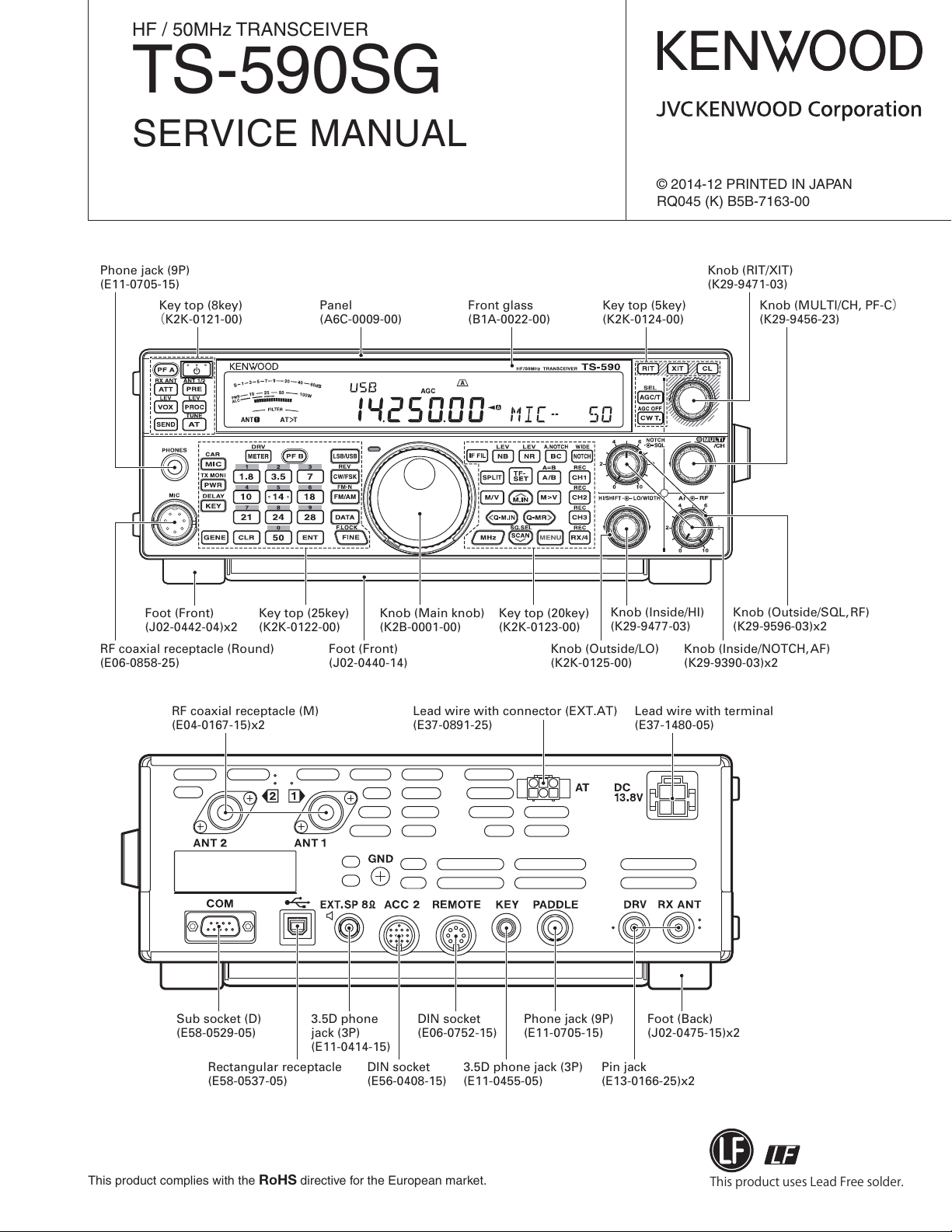
Phone jack (9P)
(E11-0705-15)
Key top (8key)
K2K-0121-00)
(
Foot (Front)
(J02-0442-04)x2
RF coaxial receptacle (Round)
(E06-0858-25)
RF coaxial receptacle (M)
(E04-0167-15)x2
Key top (25key)
(K2K-0122-00)
Panel
(A6C-0009-00)
Knob (Main knob)
(K2B-0001-00)
Foot (Front)
(J02-0440-14)
Front glass
(B1A-0022-00)
Key top (20key)
(K2K-0123-00)
Knob (Outside/LO)
(K2K-0125-00)
Lead wire with connector (EXT.AT)
(E37-0891-25)
Key top (5key)
(K2K-0124-00)
Knob (RIT/XIT)
(K29-9471-03)
Knob (Inside/HI)
(K29-9477-03)
Knob (Inside/NOTCH,AF)
(K29-9390-03)x2
Lead wire with terminal
(E37-1480-05)
Knob (MULTI/CH, PF-C
(K29-9456-23)
Knob (Outside/SQL,RF)
(K29-9596-03)x2
)
Sub socket (D)
(E58-0529-05)
Rectangular receptacle
(E58-0537-05)
This product complies with the
3.5D phone
jack (3P)
(E11-0414-15)
DIN socket
(E56-0408-15)
directive for the European market.
RoHS
DIN socket
(E06-0752-15)
3.5D phone jack (3P)
(E11-0455-05)
Phone jack (9P)
(E11-0705-15)
Foot (Back)
(J02-0475-15)x2
Pin jack
(E13-0166-25)x2
ThisproductusesLeadFreesolder.
TS-590SG
DISASSEMBLY FOR REPAIR .................................................. 3
CIRCUIT DESCRIPTION .......................................................... 5
COMPONENTS DESCRIPTION ............................................. 20
SEMICONDUCTOR DATA ...................................................... 27
PARTS LIST ............................................................................ 34
EXPLODED VIEW ................................................................... 63
PACKING ................................................................................ 66
ADJUSTMENT ........................................................................ 67
TERMINAL FUNCTION .......................................................... 81
PC BOARD
FINAL UNIT (X45-391X-XX) ................................................ 88
CONTROL UNIT (XC1-021X-XX) (A/3) ............................... 92
CONTROL UNIT (XC1-021X-XX) (B,C/3) ........................... 96
CONTENTS
DISPLAY UNIT (XC1-0220-00) .......................................... 100
TX-RX UNIT (XC1-024X-XX) ............................................. 104
INTERCONNECTION DIAGRAM .......................................... 108
SCHEMATIC DIAGRAM ....................................................... 110
BLOCK DIAGRAM ................................................................ 136
LEVEL DIAGRAM ................................................................. 138
OPTIONAL ACCESSORIES
PS-60 (DC Power Supply) ................................................ 140
ARCP-590G (Radio Control Program) ............................ 140
ARHP-590G (Radio Host Program) ................................. 140
ARUA-10 (USB Audio Controller) ................................... 140
SPECIFICATIONS ................................................................. 141
Document Copyrights
Copyright 2014 by JVC KENWOOD Corporation. All
rights reserved.
No part of this manual may be reproduced, translated,
distributed, or transmitted in any form or by any means,
electronic, mechanical, photocopying, recording, or other-
wise, for any purpose without the prior written permission of
JVC KENWOOD Corporation.
2
Disclaimer
While every precaution has been taken in the prepara-
tion of this manual, JVC KENWOOD Corporation assumes
no responsibility for errors or omissions. Neither is any li-
ability assumed for damages resulting from the use of the
information contained herein. JVC KENWOOD Corporation
reserves the right to make changes to any products herein
at any time for improvement purposes.
DISASSEMBLY FOR REPAIR
TS-590SG
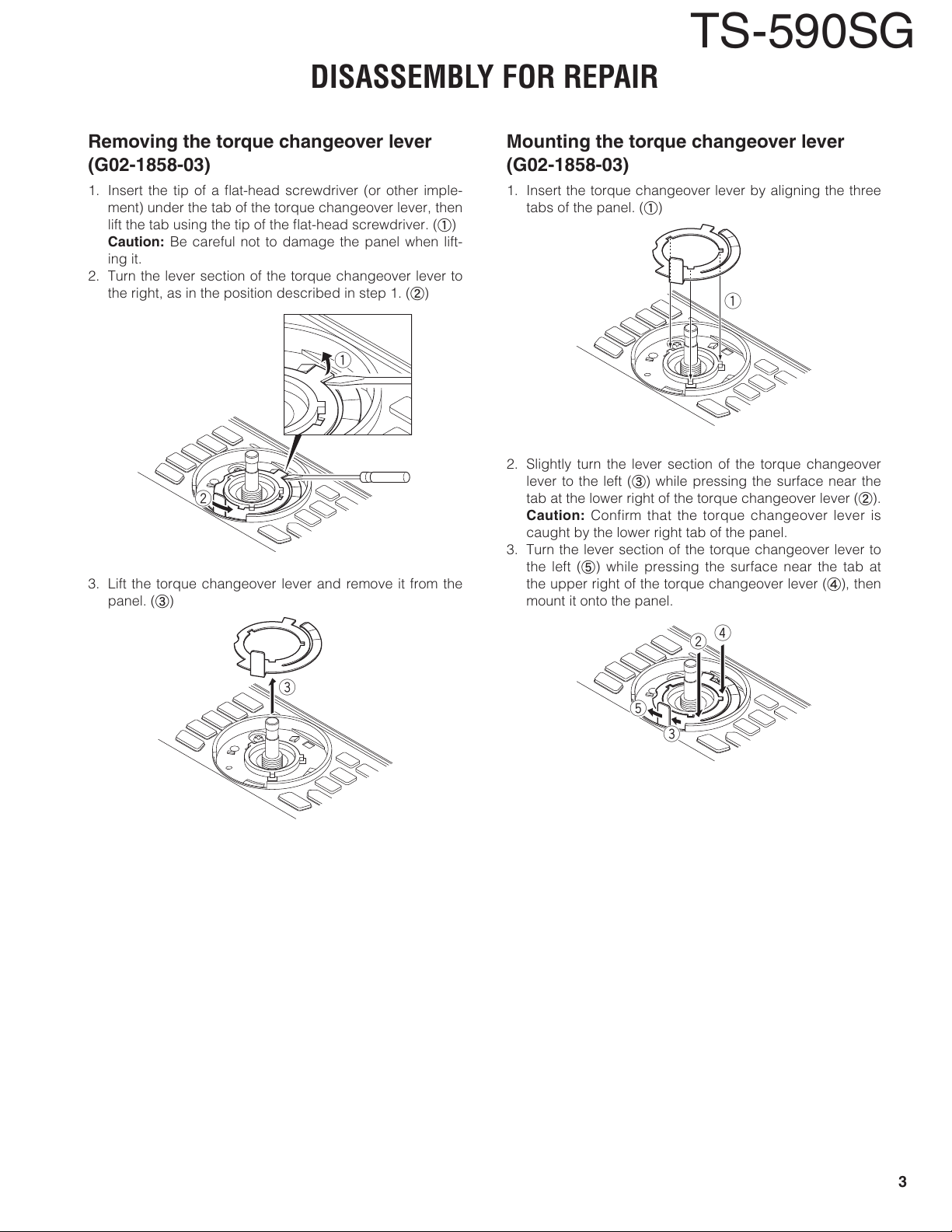
Removing the torque changeover lever (G02-1858-03)
1. Insert the tip of a fl at-head screwdriver (or other imple-
ment) under the tab of the torque changeover lever, then
lift the tab using the tip of the fl at-head screwdriver. (a)
Caution:
ing it.
2. Turn the lever section of the torque changeover lever to
the right, as in the position described in step 1. (b)
3. Lift the torque changeover lever and remove it from the
panel. (c)
Be careful not to damage the panel when lift-
:
@
Mounting the torque changeover lever (G02-1858-03)
1. Insert the torque changeover lever by aligning the three
tabs of the panel. (a)
:
2. Slightly turn the lever section of the torque changeover
lever to the left (c) while pressing the surface near the
tab at the lower right of the torque changeover lever (b).
Caution:
caught by the lower right tab of the panel.
3. Turn the lever section of the torque changeover lever to
the left (e) while pressing the surface near the tab at
the upper right of the torque changeover lever (d), then
mount it onto the panel.
Confirm that the torque changeover lever is
.
=
.
@
;
3
TS-590SG
DISASSEMBLY FOR REPAIR
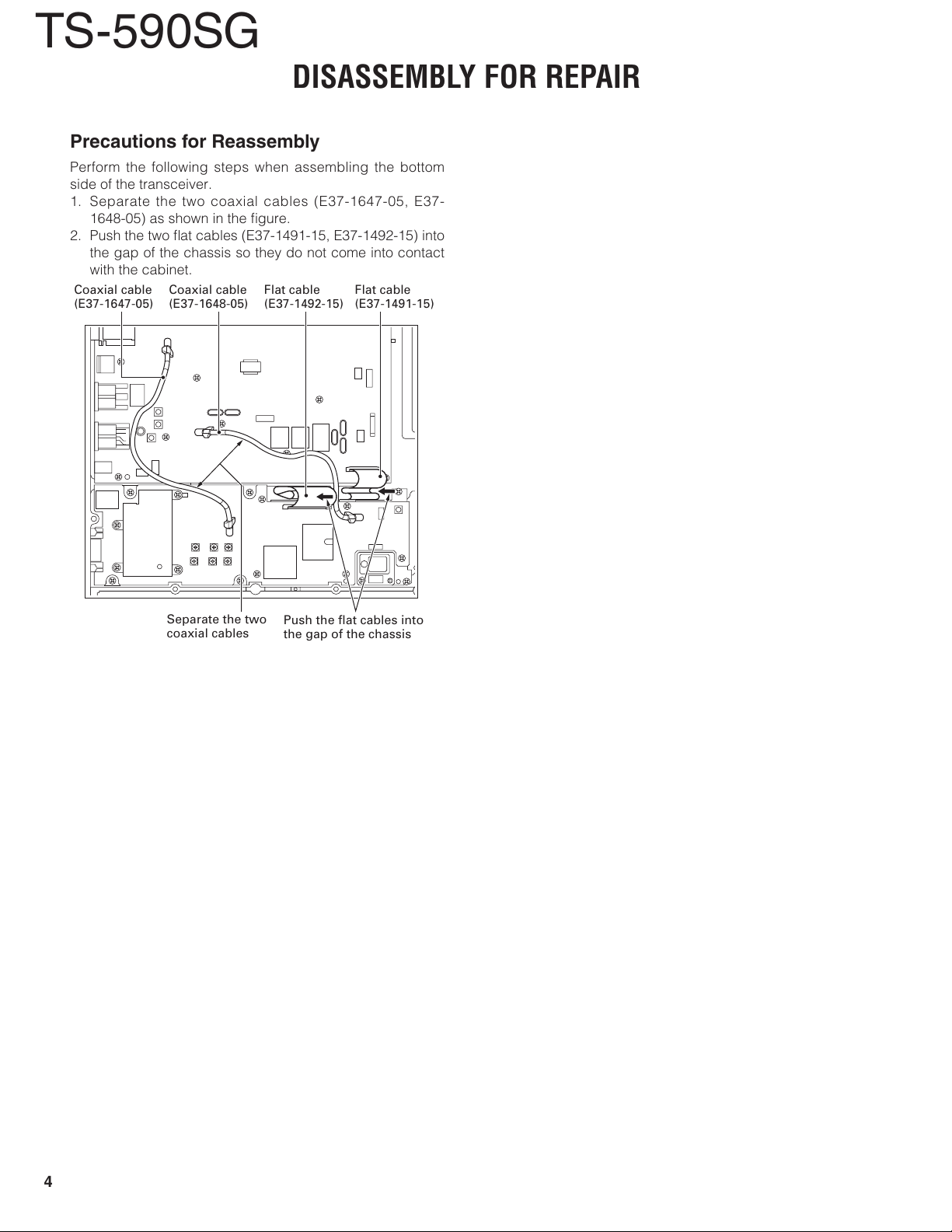
Precautions for Reassembly
Perform the following steps when assembling the bottom
side of the transceiver.
1. Separate the two coaxial cables (E37-1647-05, E37-
1648-05) as shown in the fi gure.
2. Push the two fl at cables (E37-1491-15, E37-1492-15) into
the gap of the chassis so they do not come into contact
with the cabinet.
Coaxial cable
(E37-1647-05)
Coaxial cable
(E37-1648-05)
Flat cable
(E37-1492-15)
Flat cable
(E37-1491-15)
Separate the two
coaxial cables
Push the flat cables into
the gap of the chassis
4
CIRCUIT DESCRIPTION
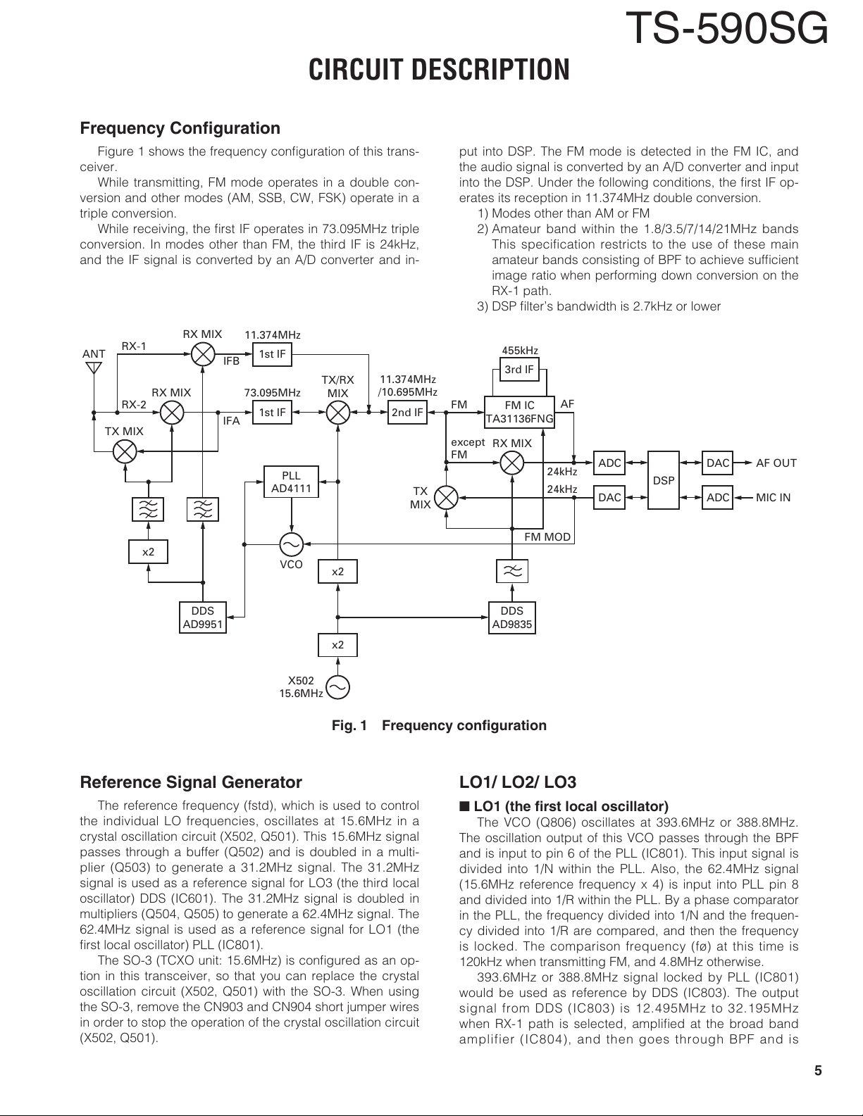
Frequency Confi guration
Figure 1 shows the frequency confi guration of this trans-
ceiver.
While transmitting, FM mode operates in a double con-
version and other modes (AM, SSB, CW, FSK) operate in a
triple conversion.
While receiving, the fi rst IF operates in 73.095MHz triple
conversion. In modes other than FM, the third IF is 24kHz,
and the IF signal is converted by an A/D converter and in-
TS-590SG
put into DSP. The FM mode is detected in the FM IC, and
the audio signal is converted by an A/D converter and input
into the DSP. Under the following conditions, the fi rst IF op-
erates its reception in 11.374MHz double conversion.
1) Modes other than AM or FM
2) Amateur band within the 1.8/3.5/7/14/21MHz bands
This specification restricts to the use of these main
amateur bands consisting of BPF to achieve suffi cient
image ratio when performing down conversion on the
RX-1 path.
3) DSP fi lter’s bandwidth is 2.7kHz or lower
ANT
RX-1
RX-2
TX MIX
RX MIX
x2
RX MIX
DDS
AD9951
11.374MHz
IFB
73.095MHz
IFA
1st IF
1st IF
AD4111
PLL
VCO
X502
15.6MHz
455kHz
TX/RX
MIX
x2
x2
11.374MHz
/10.695MHz
2nd IF
TX
MIX
FM
except
FM
3rd IF
FM IC
TA31136FNG
RX MIX
DDS
AD9835
Fig. 1 Frequency confi guration
24kHz
24kHz
FM MOD
AF
ADC
DAC
DSP
DAC
ADC
AF OUT
MIC IN
Reference Signal Generator
The reference frequency (fstd), which is used to control
the individual LO frequencies, oscillates at 15.6MHz in a
crystal oscillation circuit (X502, Q501). This 15.6MHz signal
passes through a buffer (Q502) and is doubled in a multi-
plier (Q503) to generate a 31.2MHz signal. The 31.2MHz
signal is used as a reference signal for LO3 (the third local
oscillator) DDS (IC601). The 31.2MHz signal is doubled in
multipliers (Q504, Q505) to generate a 62.4MHz signal. The
62.4MHz signal is used as a reference signal for LO1 (the
fi rst local oscillator) PLL (IC801).
The SO-3 (TCXO unit: 15.6MHz) is confi gured as an op-
tion in this transceiver, so that you can replace the crystal
oscillation circuit (X502, Q501) with the SO-3. When using
the SO-3, remove the CN903 and CN904 short jumper wires
in order to stop the operation of the crystal oscillation circuit
(X502, Q501).
LO1/ LO2/ LO3
n
LO1 (the fi rst local oscillator)
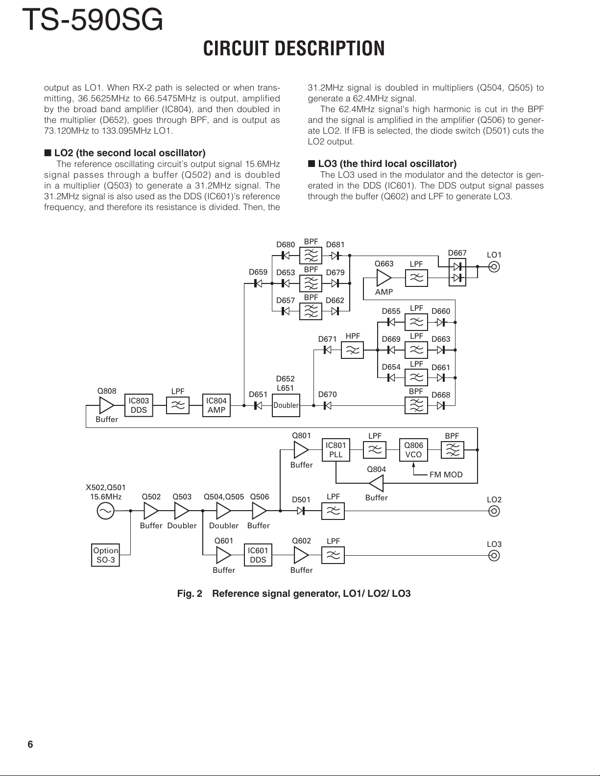
The VCO (Q806) oscillates at 393.6MHz or 388.8MHz.
The oscillation output of this VCO passes through the BPF
and is input to pin 6 of the PLL (IC801). This input signal is
divided into 1/N within the PLL. Also, the 62.4MHz signal
(15.6MHz reference frequency x 4) is input into PLL pin 8
and divided into 1/R within the PLL. By a phase comparator
in the PLL, the frequency divided into 1/N and the frequen-
cy divided into 1/R are compared, and then the frequency
is locked. The comparison frequency (fø) at this time is
120kHz when transmitting FM, and 4.8MHz otherwise.
393.6MHz or 388.8MHz signal locked by PLL (IC801)
would be used as reference by DDS (IC803). The output
signal from DDS (IC803) is 12.495MHz to 32.195MHz
when RX-1 path is selected, amplifi ed at the broad band
amplifier (IC804), and then goes through BPF and is
5
TS-590SG
CIRCUIT DESCRIPTION
output as LO1. When RX-2 path is selected or when trans-
mitting, 36.5625MHz to 66.5475MHz is output, amplified
by the broad band amplifi er (IC804), and then doubled in
the multiplier (D652), goes through BPF, and is output as
73.120MHz to 133.095MHz LO1.
n
LO2 (the second local oscillator)
The reference oscillating circuit’s output signal 15.6MHz
signal passes through a buffer (Q502) and is doubled
in a multiplier (Q503) to generate a 31.2MHz signal. The
31.2MHz signal is also used as the DDS (IC601)’s reference
frequency, and therefore its resistance is divided. Then, the
D680 D681
D659
D653
D657
D652
Q808
Buffer
X502,Q501
15.6MHz
IC803
DDS
Q502
LPF
Q503
IC804
AMP
Q504,Q505
D651
Doubler
Q506
L651
31.2MHz signal is doubled in multipliers (Q504, Q505) to
generate a 62.4MHz signal.
The 62.4MHz signal’s high harmonic is cut in the BPF
and the signal is amplifi ed in the amplifi er (Q506) to gener-
ate LO2. If IFB is selected, the diode switch (D501) cuts the
LO2 output.
n
LO3 (the third local oscillator)
The LO3 used in the modulator and the detector is gen-
erated in the DDS (IC601). The DDS output signal passes
through the buffer (Q602) and LPF to generate LO3.
BPF
BPF
BPF
Q801
Buffer
D501
D679
D662
D671
D670
IC801
LPF
PLL
HPF
Q663
AMP
D655 D660
D669
D654
LPF
Q806
VCO
Q804
Buffer
LPF
LPF
LPF
LPF
BPF
D667
D663
D661
D668
BPF
FM MOD
LO1
LO2
Option
SO-3
Buffer
Doubler
Q601
Buffer
BufferDoubler
IC601
DDS
Q602
Buffer
LPF
LO3
Fig. 2 Reference signal generator, LO1/ LO2/ LO3
6
TS-590SG
CIRCUIT DESCRIPTION
l
IF=73M
Frequency: 0.03~60MHz
HF TX/RX
LO1
Filter offset 1 +(DSPFC)/2 +1.5k/2 -(DSPFC)/2 –1.5k/2
RIT (Δ RIT)/2 - (Δ RIT)/2 - (Δ RIT)/2 - (Δ RIT)/2 -
XIT - (Δ XIT)/2 - (Δ XIT)/2 - (Δ XIT)/2 - (Δ XIT)/2
CAR correction IF10M_2.7k
HF TX/RX
LO1
Filter offset 1 –(SHIFT/2)/2 –(SHIFT/2)/2 –(SHIFT/2)/2 –(SHIFT/2)/2 0 0 0 0
RIT (Δ RIT)/2 - (Δ RIT)/2 - (Δ RIT)/2 - (Δ RIT)/2 -
XIT - (Δ XIT)/2 - (Δ XIT)/2 - (Δ XIT)/2 - (Δ XIT)/2
CAR correction IF10M_2.7k
+(CAR1)/2 +(CAR1)/2 +(CAR1)/2 +(CAR1)/2 +(CAR1)/2 +(CAR1)/2 +(CAR1)/2 +(CAR1)/2
USB LSB CW CW-R
RX TX RX TX RX TX RX TX
FSK FSK-R AM FM
RX TX RX TX RX TX RX TX
--------
DDS AD9951 (DEN1)
+(SHIFT-PITCH)/2
DDS AD9951 (DEN1)
0
–(SHIFT-PITCH)/2
0
l
IF=11M
Frequency: 0.03~21.5MHz (Amateur bands within 1.8/3.5/7/14/21MHz band only)
HF TX/RX
LO1
Filter offset 1 +(DSPFC) –(DSPFC) +(SHIFT-PITCH) –(SHIFT-PITCH) –(SHIFT/2) –(SHIFT/2)
RIT (Δ RIT) (Δ RIT) (Δ RIT) (Δ RIT) (Δ RIT) (Δ RIT)
CAR
correction
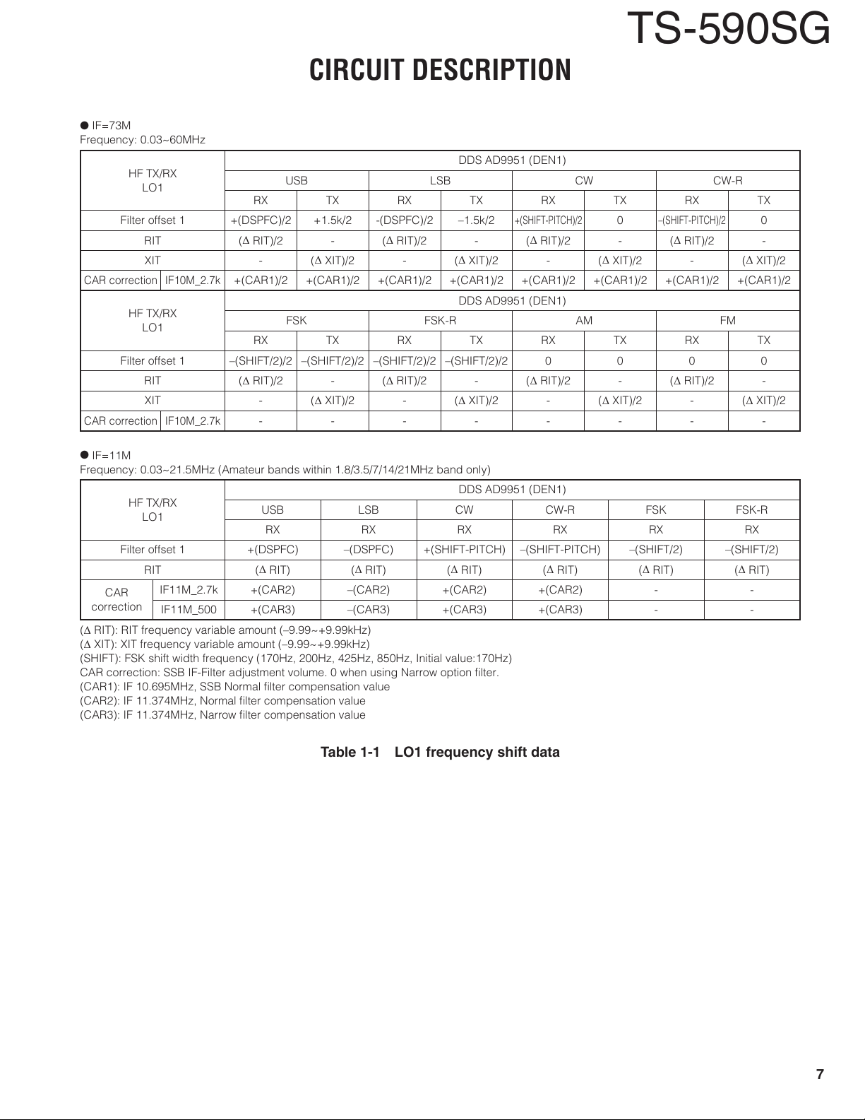
(Δ RIT): RIT frequency variable amount (–9.99~+9.99kHz)
(Δ XIT): XIT frequency variable amount (–9.99~+9.99kHz)
(SHIFT): FSK shift width frequency (170Hz, 200Hz, 425Hz, 850Hz, Initial value:170Hz)
CAR correction: SSB IF-Filter adjustment volume. 0 when using Narrow option fi lter.
(CAR1): IF 10.695MHz, SSB Normal fi lter compensation value
(CAR2): IF 11.374MHz, Normal fi lter compensation value
(CAR3): IF 11.374MHz, Narrow fi lter compensation value
IF11M_2.7k +(CAR2) –(CAR2) +(CAR2) +(CAR2) - -
IF11M_500 +(CAR3) –(CAR3) +(CAR3) +(CAR3) - -
USB LSB CW CW-R FSK FSK-R
RX RX RX RX RX RX
DDS AD9951 (DEN1)
Table 1-1 LO1 frequency shift data
7
TS-590SG
CIRCUIT DESCRIPTION
USB LSB CW CW-R
LO3
RX<21.3M,
21.5≤RX
Filter offset 1
CW pitch - - - - - - - - -
FSK tone - - - - - - - - -
CAR cor-
rection
CAR cor-
rection
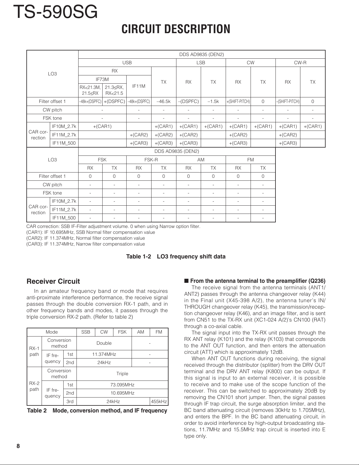
CAR correction: SSB IF-Filter adjustment volume. 0 when using Narrow option fi lter.
(CAR1): IF 10.695MHz, SSB Normal fi lter compensation value
(CAR2): IF 11.374MHz, Normal fi lter compensation value
(CAR3): IF 11.374MHz, Narrow fi lter compensation value
IF10M_2.7k +(CAR1)
IF11M_2.7k
IF11M_500
LO3
Filter offset 1 0 0 0 0 0 0 0 0
CW pitch - - - - - - - -
FSK tone - - - - - - - -
IF10M_2.7k - - - - ----
IF11M_2.7k - - - - - - - -
IF11M_500 - - - - - - - -
–48k+(DSPFC)
RX TX RX TX RX TX RX TX
RX
IF73M
21.3≤RX,
RX<21.5
+(DSPFC)
FSK FSK-R AM FM
IF11M
–48k+(DSPFC)
+(CAR2) +(CAR2) +
+(CAR3) +(CAR3) +
TX RX TX RX TX RX TX
–46.5k –(DSPFC) –1.5k
+(CAR1) +
DDS AD9835 (DEN2)
DDS AD9835 (DEN2)
(CAR1)+(CAR1)
(CAR2)
(CAR3)
+(SHIFT-PITCH)
+(CAR1) +(CAR1) +(CAR1) +(CAR1)
+(CAR2) +(CAR2)
+(CAR3) +(CAR3)
0
–(SHIFT-PITCH)
0
Table 1-2 LO3 frequency shift data
Receiver Circuit
In an amateur frequency band or mode that requires
anti-proximate interference performance, the receive signal
passes through the double conversion RX-1 path, and in
other frequency bands and modes, it passes through the
triple conversion RX-2 path. (Refer to table 2)
Mode SSB CW FSK AM FM
RX-1
path
RX-2
path
Table 2
Conversion
method
IF fre-
quency
Conversion
IF fre-
quency
1st 11.374MHz -
2nd 24kHz -
method
1st 73.095MHz
2nd 10.695MHz
3rd 24kHz 455kHz
Mode, conversion method, and IF frequency
Double -
Triple
n
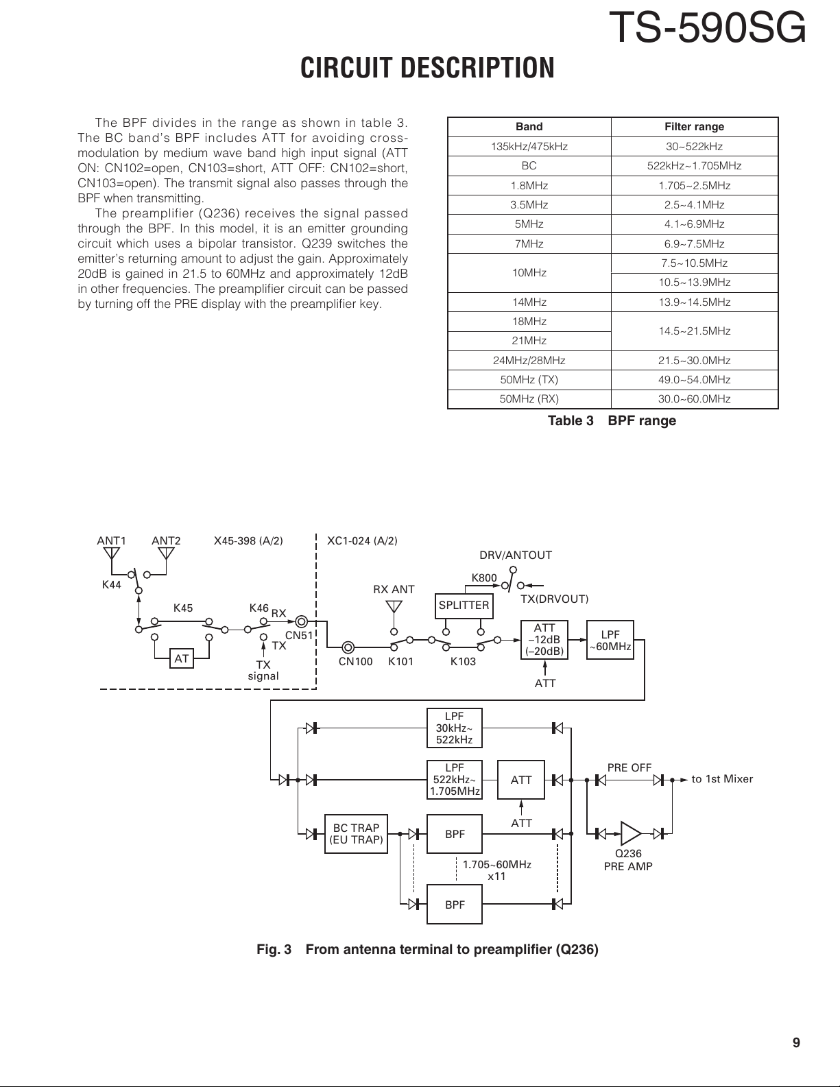
From the antenna terminal to the preamplifi er (Q236)
The receive signal from the antenna terminals (ANT1/
ANT2) passes through the antenna changeover relay (K44)
in the Final unit (X45-398 A/2), the antenna tuner’s IN/
THROUGH changeover relay (K45), the transmission/recep-
tion changeover relay (K46), and an image fi lter, and is sent
from CN51 to the TX-RX unit (XC1-024 A/2)’s CN100 (RAT)
through a co-axial cable.
The signal input into the TX-RX unit passes through the
RX ANT relay (K101) and the relay (K103) that corresponds
to the ANT OUT function, and then enters the attenuation
circuit (ATT) which is approximately 12dB.
When ANT OUT functions during receiving, the signal
received through the distributor (splitter) from the DRV OUT
terminal and the DRV ANT relay (K800) can be output. If
this signal is input to an external receiver, it is possible
to receive and to make use of the scope function of the
receiver. This can be switched to approximately 20dB by
removing the CN101 short jumper. Then, the signal passes
through IF trap circuit, the surge absorption limiter, and the
BC band attenuating circuit (removes 30kHz to 1.705MHz),
and enters the BPF. In the BC band attenuating circuit, in
order to avoid interference by high-output broadcasting sta-
tions, 11.7MHz and 15.5MHz trap circuit is inserted into E
type only.
8
CIRCUIT DESCRIPTION
TS-590SG
The BPF divides in the range as shown in table 3.
The BC band’s BPF includes ATT for avoiding cross-
modulation by medium wave band high input signal (ATT
ON: CN102=open, CN103=short, ATT OFF: CN102=short,
CN103=open). The transmit signal also passes through the
BPF when transmitting.
The preamplifier (Q236) receives the signal passed
through the BPF. In this model, it is an emitter grounding
circuit which uses a bipolar transistor. Q239 switches the
emitter’s returning amount to adjust the gain. Approximately
20dB is gained in 21.5 to 60MHz and approximately 12dB
in other frequencies. The preamplifi er circuit can be passed
by turning off the PRE display with the preamplifi er key.
Band Filter range
135kHz/475kHz 30~522kHz
BC 522kHz~1.705MHz
1.8MHz 1.705~2.5MHz
3.5MHz 2.5~4.1MHz
5MHz 4.1~6.9MHz
7MHz 6.9~7.5MHz
10MHz
14MHz 13.9~14.5MHz
18MHz
21MHz
24MHz/28MHz 21.5~30.0MHz
50MHz (TX) 49.0~54.0MHz
50MHz (RX) 30.0~60.0MHz
7.5~10.5MHz
10.5~13.9MHz
14.5~21.5MHz
Table 3 BPF range
ANT1 ANT2
K44
AT
K46K45
TX
signal
RX
TX
CN51
XC1-024 (A/2)X45-398 (A/2)
RX ANT
SPLITTER
CN100 K101 K103
30kHz~
522kHz
522kHz~
1.705MHz
BC TRAP
(EU TRAP)
DRV/ANTOUT
K800
LPF
LPF
BPF
1.705~60MHz
BPF
ATT
ATT
x11
TX(DRVOUT)
ATT
–12dB
(–20dB)
ATT
LPF
~60MHz
PRE OFF
to 1st Mixer
Q236
PRE AMP
Fig. 3 From antenna terminal to preamplifi er (Q236)
9
TS-590SG
CIRCUIT DESCRIPTION
n
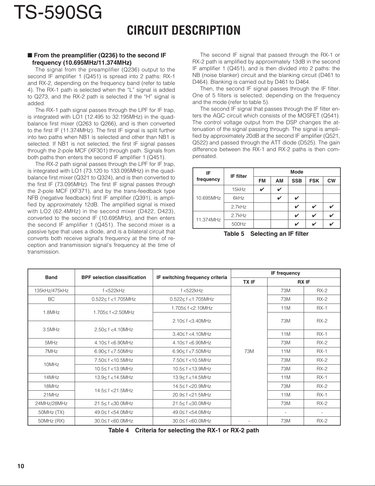
From the preamplifi er (Q236) to the second IF
frequency (10.695MHz/11.374MHz)
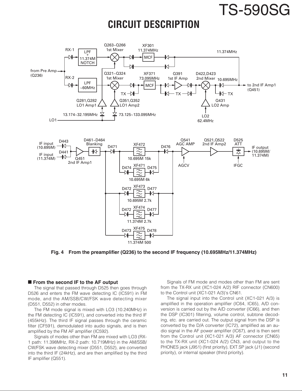
The signal from the preamplifier (Q236) output to the
second IF amplifi er 1 (Q451) is spread into 2 paths: RX-1
and RX-2, depending on the frequency band (refer to table
4). The RX-1 path is selected when the “L” signal is added
to Q273, and the RX-2 path is selected if the “H” signal is
added.
The RX-1 path signal passes through the LPF for IF trap,
is integrated with LO1 (12.495 to 32.195MHz) in the quad-
balance fi rst mixer (Q263 to Q266), and is then converted
to the fi rst IF (11.374MHz). The fi rst IF signal is split further
into two paths when NB1 is selected and other than NB1 is
selected. If NB1 is not selected, the fi rst IF signal passes
through the 2-pole MCF (XF301) through path. Signals from
both paths then enters the second IF amplifi er 1 (Q451).
The RX-2 path signal passes through the LPF for IF trap,
is integrated with LO1 (73.120 to 133.095MHz) in the quad-
balance fi rst mixer (Q321 to Q324), and is then converted to
the fi rst IF (73.095MHz). The fi rst IF signal passes through
the 2-pole MCF (XF371), and by the trans-feedback type
NFB (negative feedback) fi rst IF amplifi er (Q391), is ampli-
fi ed by approximately 12dB. The amplifi ed signal is mixed
with LO2 (62.4MHz) in the second mixer (D422, D423),
converted to the second IF (10.695MHz), and then enters
the second IF amplifier 1 (Q451). The second mixer is a
passive type that uses a diode, and is a bilateral circuit that
converts both receive signal's frequency at the time of re-
ception and transmission signal's frequency at the time of
transmission.
The second IF signal that passed through the RX-1 or
RX-2 path is amplifi ed by approximately 13dB in the second
IF amplifi er 1 (Q451), and is then divided into 2 paths: the
NB (noise blanker) circuit and the blanking circuit (D461 to
D464). Blanking is carried out by D461 to D464.
Then, the second IF signal passes through the IF fi lter.
One of 5 filters is selected, depending on the frequency
and the mode (refer to table 5).
The second IF signal that passes through the IF fi lter en-
ters the AGC circuit which consists of the MOSFET (Q541).
The control voltage output from the DSP changes the at-
tenuation of the signal passing through. The signal is ampli-
fi ed by approximately 20dB at the second IF amplifi er (Q521,
Q522) and passed through the ATT diode (D525). The gain
difference between the RX-1 and RX-2 paths is then com-
pensated.
IF
frequency
10.695MHz
11.374MHz
IF fi lter
15kHz
6kHz
2.7kHz
2.7kHz
500Hz
FM AM SSB FSK CW
4 4
Mode
44
444
444
444
Table 5 Selecting an IF fi lter
Band BPF selection classifi cation IF switching frequency criteria
135kHz/475kHz f <522kHz f <522kHz
BC 0.522≤ f <1.705MHz 0.522≤ f <1.705MHz 73M RX-2
1.8MHz 1.705≤ f <2.50MHz
3.5MHz 2.50≤ f <4.10MHz
5MHz 4.10≤ f <6.90MHz 4.10≤ f <6.90MHz 73M RX-2
7MHz 6.90≤ f <7.50MHz 6.90≤ f <7.50MHz 11M RX-1
10MHz
14MHz 13.9≤ f <14.5MHz 13.9≤ f <14.5MHz 11M RX-1
18MHz
21MHz 20.9≤ f <21.5MHz 11M RX-1
24MHz/28MHz 21.5≤ f <30.0MHz 21.5≤ f <30.0MHz 73M RX-2
50MHz (TX) 49.0≤ f <54.0MHz 49.0≤ f <54.0MHz - -
50MHz (RX) 30.0≤ f <60.0MHz 30.0≤ f <60.0MHz - 73M RX-2
7.50≤ f <10.5MHz 7.50≤ f <10.5MHz 73M RX-2
10.5≤ f <13.9MHz 10.5≤ f <13.9MHz 73M RX-2
14.5≤ f <21.5MHz
1.705≤ f <2.10MHz 11M RX-1
2.10≤ f <3.40MHz 73M RX-2
3.40≤ f <4.10MHz 11M RX-1
14.5≤ f
20.9MHz 73M RX-2
<
TX IF RX IF
73M
IF frequency
73M RX-2
Table 4 Criteria for selecting the RX-1 or RX-2 path
10
CIRCUIT DESCRIPTION
TS-590SG
from Pre Amp
(Q236)
LO1
IF input
(10.695M)
IF input
(11.374M)
RX-1
RX-2
D443
D441
2nd IF Amp1
LPF
+
11.374M
NOTCH
LPF
~60MHz
Q281,Q282
LO1 Amp1
D461~D464
Blanking
Q451
Q263~Q266
1st Mixer
Q321~Q324
1st Mixer
TX
Q351,Q352
LO1 Amp2
73.125~133.095MHz13.174~32.195MHz
D471
11.374MHz
73.095MHz
XF472
10.695M 15k
XF471
10.695M 6k
XF473
XF301
MCF
XF371
MCF
D475D474
D477D472
1st IF Amp
D476
11.374MHz
Q391
TX TX
Q541
AGC AMP
AGCV
D422,D423
2nd Mixer
LO2 Amp
LO2
62.4MHz
Q521,Q522
2nd IF Amp2
10.695MHz
Q431
D525
ATT
IFGC
to 2nd IF Amp1
(Q451)
IF output
(10.695M/
11.374M)
10.695M 2.7k
XF474
11.374M 2.7k
XF475
11.374M 500
Fig. 4 From the preamplifi er (Q236) to the second IF frequency (10.695MHz/11.374MHz)
n
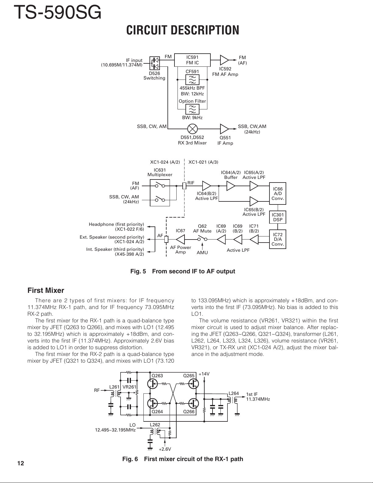
From the second IF to the AF output
The signal that passed through D525 then goes through
D526 and enters the FM wave detecting IC (IC591) in FM
mode, and the AM/SSB/CW/FSK wave detecting mixer
(D551, D552) in other modes.
The FM mode signal is mixed with LO3 (10.240MHz) in
the FM detecting IC (IC591), and converted into the third IF
(455kHz). The third IF signal passes through the ceramic
fi lter (CF591), demodulated into audio signals, and is then
amplifi ed by the FM AF amplifi er (IC592).
Signals of modes other than FM are mixed with LO3 (RX-
1 path: 11.398MHz, RX-2 path: 10.719MHz) in the AM/SSB/
CW/FSK wave detecting mixer (D551, D552), are converted
into the third IF (24kHz), and are then amplifi ed by the third
IF amplifi er (Q551).
D477D472
D478D473
Signals of FM mode and modes other than FM are sent
from the TX-RX unit (XC1-024 A/2) RIF connector (CN600)
to the Control unit (XC1-021 A/3)’s CN61.
The signal input into the Control unit (XC1-021 A/3) is
amplifi ed in the operation amplifi er (IC64, IC65), A/D con-
version is carried out by the A/D converter (IC66), and then
the DSP (IC301) fi ltering, volume control, subtone decod-
ing, etc. are carried out. The output signal from the DSP is
converted by the D/A converter (IC72), amplifi ed as an au-
dio signal in the AF power amplifi er (IC67), and is then sent
from the Control unit (XC1-021 A/3) AF connector (CN65)
to the TX-RX unit (XC1-024 A/2) CN3, and output to the
PHONES jack (J951) (fi rst priority), EXT.SP jack (J1) (second
priority), or internal speaker (third priority).
11
TS-590SG
CIRCUIT DESCRIPTION
(10.695M/11.374M)
Headphone (first priority)
Ext. Speaker (second priority)
Int. Speaker (third priority)
IF input
FM
(AF)
SSB, CW, AM
(24kHz)
(XC1-022 F/6)
(XC1-024 A/2)
(X45-398 A/2)
SSB, CW, AM
FM
D526
Switching
XC1-024 (A/2) XC1-021 (A/3)
IC631
Multiplexer
AF
CF591
455kHz BPF
BW: 12kHz
Option Filter
BW: 9kHz
D551,D552
RX 3rd Mixer
IC67
AF Power
Amp
IC591
FM IC
RIF
AF Mute
IC64(B/2)
Active LPF
Q62
AMU
IC592
FM AF Amp
Q551
IF Amp
IC64(A/2)
Buffer
IC69
IC69
(B/2)
(A/2)
Active LPF
FM
(AF)
SSB, CW,AM
(24kHz)
IC65(A/2)
Active LPF
IC65(B/2)
Active LPF
IC71
(B/2)
IC66
A/D
Conv.
IC301
DSP
IC72
D/A
Conv.
Fig. 5 From second IF to AF output
First Mixer
There are 2 types of first mixers: for IF frequency
11.374MHz RX-1 path, and for IF frequency 73.095MHz
RX-2 path.
The fi rst mixer for the RX-1 path is a quad-balance type
mixer by JFET (Q263 to Q266), and mixes with LO1 (12.495
to 32.195MHz) which is approximately +18dBm, and con-
verts into the fi rst IF (11.374MHz). Approximately 2.6V bias
is added to LO1 in order to suppress distortion.
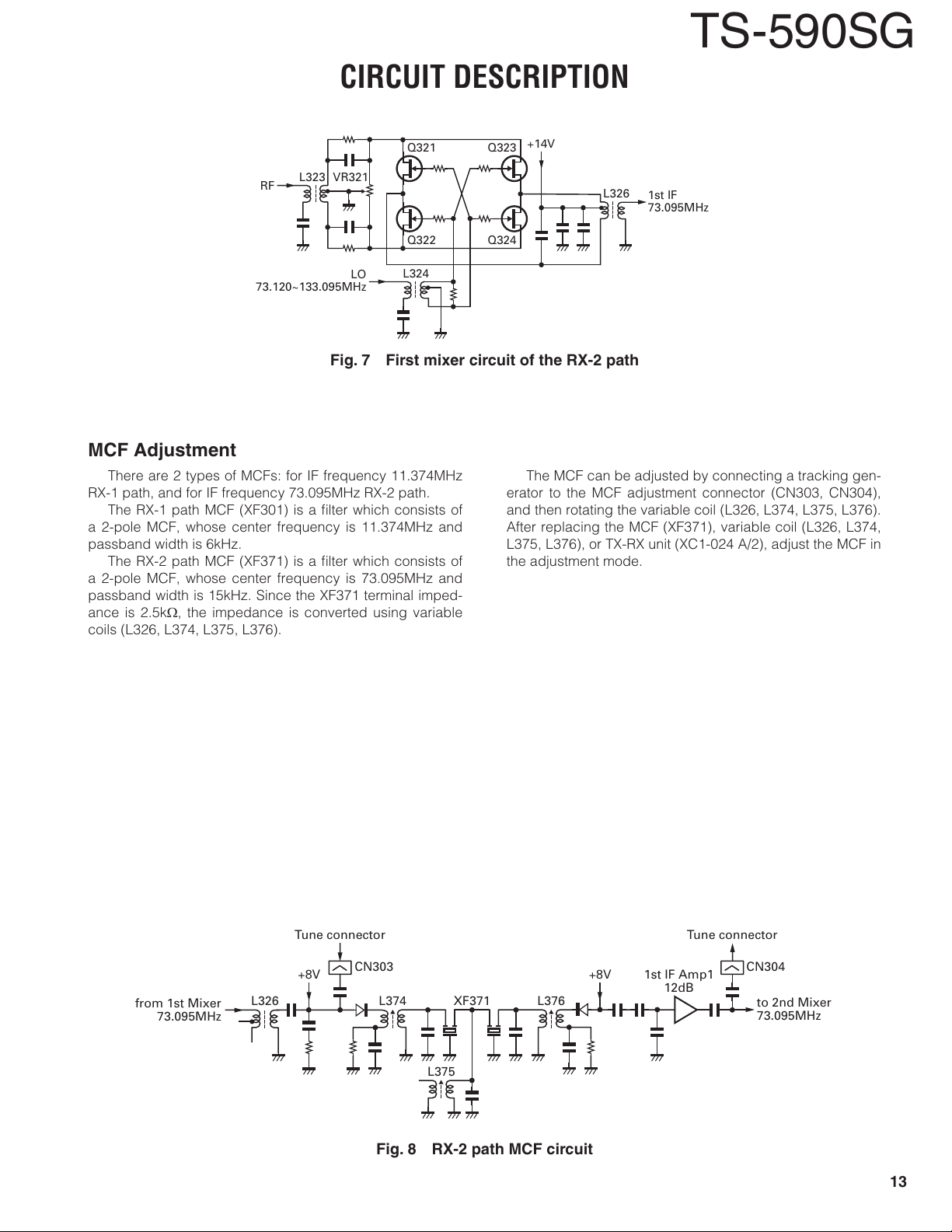
The fi rst mixer for the RX-2 path is a quad-balance type
mixer by JFET (Q321 to Q324), and mixes with LO1 (73.120
Q263 Q265
L261
RF
12.495~32.195MHz
VR261
LO
Q264 Q266
L262
to 133.095MHz) which is approximately +18dBm, and con-
verts into the fi rst IF (73.095MHz). No bias is added to this
LO1.
The volume resistance (VR261, VR321) within the first
mixer circuit is used to adjust mixer balance. After replac-
ing the JFET (Q263~Q266, Q321~Q324), transformer (L261,
L262, L264, L323, L324, L326), volume resistance (VR261,
VR321), or TX-RX unit (XC1-024 A/2), adjust the mixer bal-
ance in the adjustment mode.
+14V
L264
1st IF
11.374MHz
12
+2.6V
Fig. 6 First mixer circuit of the RX-1 path
CIRCUIT DESCRIPTION
TS-590SG
Q321 Q323
L323
RF
73.120~133.095MHz
VR321
LO
Q322 Q324
L324
Fig. 7 First mixer circuit of the RX-2 path
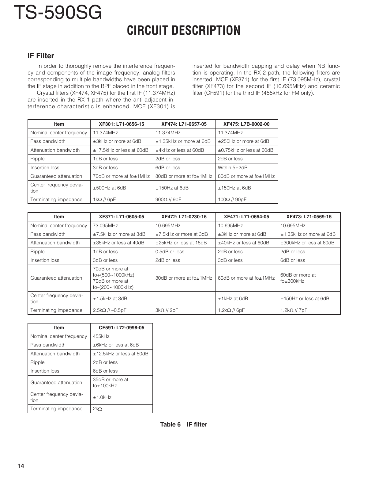
MCF Adjustment
There are 2 types of MCFs: for IF frequency 11.374MHz
RX-1 path, and for IF frequency 73.095MHz RX-2 path.
The RX-1 path MCF (XF301) is a fi lter which consists of
a 2-pole MCF, whose center frequency is 11.374MHz and
passband width is 6kHz.
The RX-2 path MCF (XF371) is a fi lter which consists of
a 2-pole MCF, whose center frequency is 73.095MHz and
passband width is 15kHz. Since the XF371 terminal imped-
ance is 2.5k, the impedance is converted using variable
coils (L326, L374, L375, L376).
+14V
L326
1st IF
73.095MHz
The MCF can be adjusted by connecting a tracking gen-
erator to the MCF adjustment connector (CN303, CN304),
and then rotating the variable coil (L326, L374, L375, L376).
After replacing the MCF (XF371), variable coil (L326, L374,
L375, L376), or TX-RX unit (XC1-024 A/2), adjust the MCF in
the adjustment mode.
from 1st Mixer
73.095MHz
Tune connector Tune connector
+8V
CN303
L375
+8V
L376XF371L374L326
1st IF Amp1
12dB
CN304
to 2nd Mixer
73.095MHz
Fig. 8 RX-2 path MCF circuit
13
TS-590SG
CIRCUIT DESCRIPTION
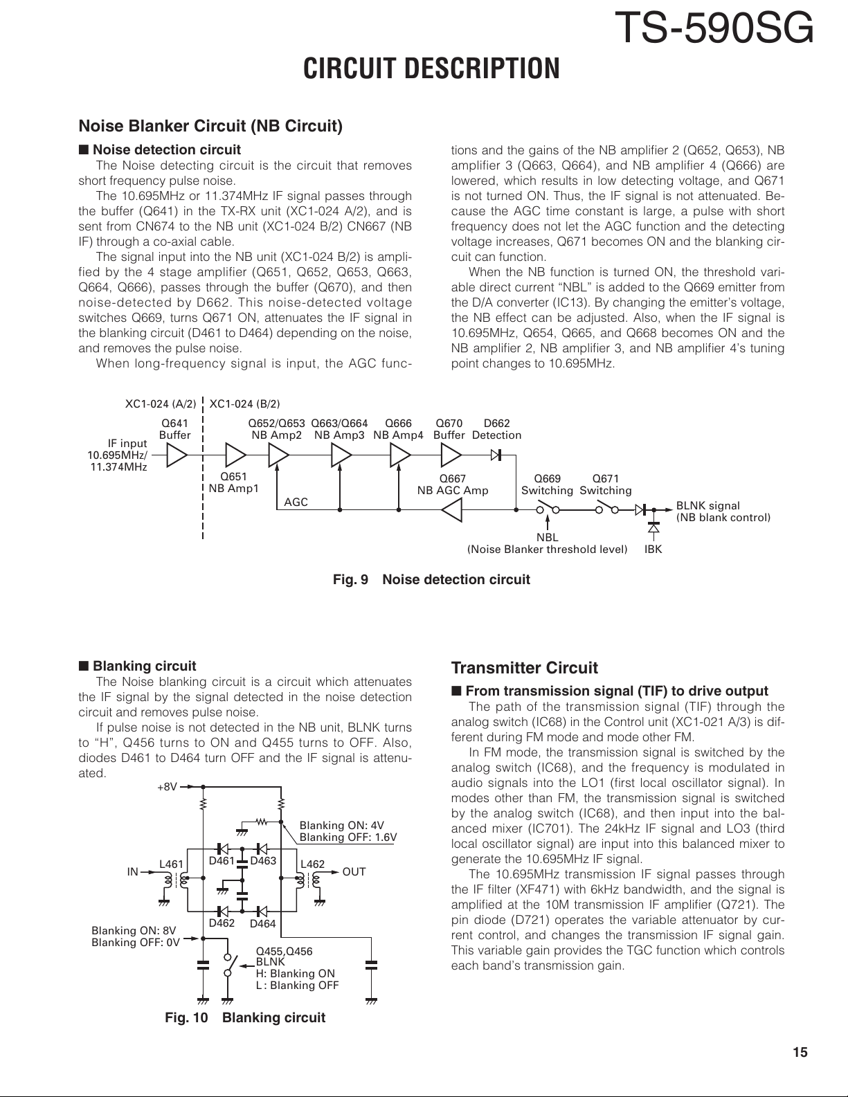
IF Filter
In order to thoroughly remove the interference frequen-
cy and components of the image frequency, analog fi lters
corresponding to multiple bandwidths have been placed in
the IF stage in addition to the BPF placed in the front stage.
Crystal fi lters (XF474, XF475) for the fi rst IF (11.374MHz)
are inserted in the RX-1 path where the anti-adjacent in-
terference characteristic is enhanced. MCF (XF301) is
Item XF301: L71-0656-15 XF474: L71-0657-05 XF475: L7B-0002-00
Nominal center frequency 11.374MHz 11.374MHz 11.374MHz
Pass bandwidth ±3kHz or more at 6dB ±1.35kHz or more at 6dB ±250Hz or more at 6dB
Attenuation bandwidth ±17.5kHz or less at 60dB ±4kHz or less at 60dB ±0.75kHz or less at 60dB
Ripple 1dB or less 2dB or less 2dB or less
Insertion loss 3dB or less 6dB or less Within 5±2dB
Guaranteed attenuation 70dB or more at fo±1MHz 80dB or more at fo±1MHz 80dB or more at fo±1MHz
Center frequency devia-
tion
Terminating impedance 1k // 6pF 900 // 9pF 100 // 90pF
±500Hz at 6dB ±150Hz at 6dB ±150Hz at 6dB
inserted for bandwidth capping and delay when NB func-
tion is operating. In the RX-2 path, the following fi lters are
inserted: MCF (XF371) for the fi rst IF (73.095MHz), crystal
fi lter (XF473) for the second IF (10.695MHz) and ceramic
fi lter (CF591) for the third IF (455kHz for FM only).
Item XF371: L71-0605-05 XF472: L71-0230-15 XF471: L71-0664-05 XF473: L71-0569-15
Nominal center frequency 73.095MHz 10.695MHz 10.695MHz 10.695MHz
Pass bandwidth ±7.5kHz or more at 3dB ±7.5kHz or more at 3dB ±3kHz or more at 6dB ±1.35kHz or more at 6dB
Attenuation bandwidth ±35kHz or less at 40dB ±25kHz or less at 18dB ±40kHz or less at 60dB ±300kHz or less at 60dB
Ripple 1dB or less 0.5dB or less 2dB or less 2dB or less
Insertion loss 3dB or less 2dB or less 3dB or less 6dB or less
70dB or more at
Guaranteed attenuation
Center frequency devia-
tion
Terminating impedance 2.5k // –0.5pF 3k // 2pF 1.2k // 6pF 1.2k // 7pF
Item CF591: L72-0998-05
Nominal center frequency 455kHz
Pass bandwidth ±6kHz or less at 6dB
Attenuation bandwidth ±12.5kHz or less at 50dB
Ripple 2dB or less
Insertion loss 6dB or less
Guaranteed attenuation
Center frequency devia-
tion
Terminating impedance 2k
fo+(500~1000kHz)
70dB or more at
fo–(200~1000kHz)
±1.5kHz at 3dB - ±1kHz at 6dB ±150Hz or less at 6dB
35dB or more at
fo±100kHz
±1.0kHz
30dB or more at fo±1MHz 60dB or more at fo±1MHz
60dB or more at
fo±300kHz
14
Table 6 IF fi lter
CIRCUIT DESCRIPTION
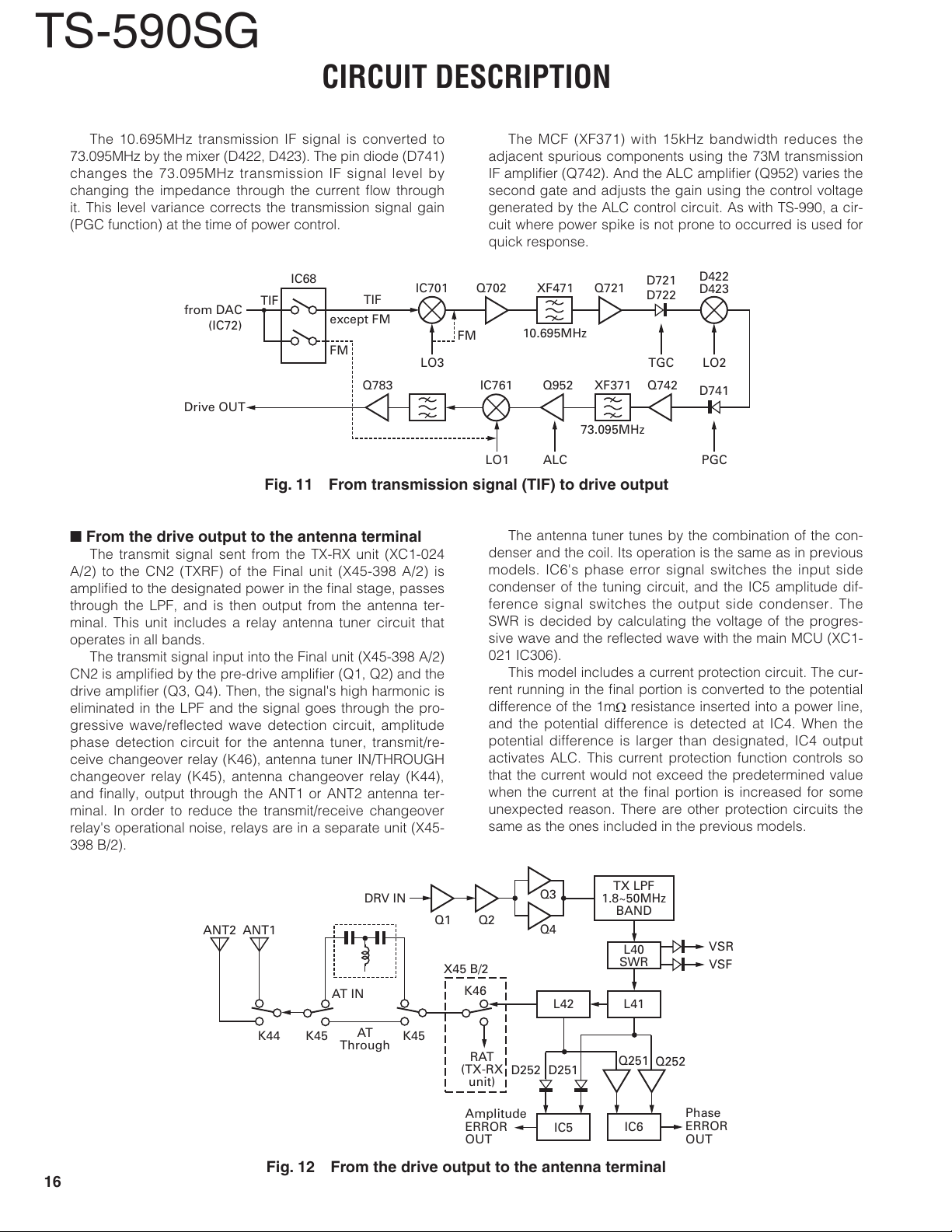
Noise Blanker Circuit (NB Circuit)
n
Noise detection circuit
The Noise detecting circuit is the circuit that removes
short frequency pulse noise.
The 10.695MHz or 11.374MHz IF signal passes through
the buffer (Q641) in the TX-RX unit (XC1-024 A/2), and is
sent from CN674 to the NB unit (XC1-024 B/2) CN667 (NB
IF) through a co-axial cable.
The signal input into the NB unit (XC1-024 B/2) is ampli-
fied by the 4 stage amplifier (Q651, Q652, Q653, Q663,
Q664, Q666), passes through the buffer (Q670), and then
noise-detected by D662. This noise-detected voltage
switches Q669, turns Q671 ON, attenuates the IF signal in
the blanking circuit (D461 to D464) depending on the noise,
and removes the pulse noise.
When long-frequency signal is input, the AGC func-
XC1-024 (A/2) XC1-024 (B/2)
IF input
10.695MHz/
11.374MHz
Q641
Buffer
Q651
NB Amp1
Q652/Q653
NB Amp2
AGC
Q663/Q664
NB Amp3
Q666
NB Amp4
TS-590SG
tions and the gains of the NB amplifi er 2 (Q652, Q653), NB
amplifier 3 (Q663, Q664), and NB amplifier 4 (Q666) are
lowered, which results in low detecting voltage, and Q671
is not turned ON. Thus, the IF signal is not attenuated. Be-
cause the AGC time constant is large, a pulse with short
frequency does not let the AGC function and the detecting
voltage increases, Q671 becomes ON and the blanking cir-
cuit can function.
When the NB function is turned ON, the threshold vari-
able direct current “NBL” is added to the Q669 emitter from
the D/A converter (IC13). By changing the emitter’s voltage,
the NB effect can be adjusted. Also, when the IF signal is
10.695MHz, Q654, Q665, and Q668 becomes ON and the
NB amplifi er 2, NB amplifi er 3, and NB amplifi er 4’s tuning
point changes to 10.695MHz.
Q670
Buffer
Q667
NB AGC Amp
D662
Detection
Q669
Switching
NBL
(Noise Blanker threshold level)
Q671
Switching
BLNK signal
(NB blank control)
IBK
Fig. 9 Noise detection circuit
n
Blanking circuit
The Noise blanking circuit is a circuit which attenuates
the IF signal by the signal detected in the noise detection
circuit and removes pulse noise.
If pulse noise is not detected in the NB unit, BLNK turns
to “H”, Q456 turns to ON and Q455 turns to OFF. Also,
diodes D461 to D464 turn OFF and the IF signal is attenu-
ated.
Blanking ON: 8V
Blanking OFF: 0V
+8V
D461
D462
Blanking ON: 4V
Blanking OFF: 1.6V
D463
D464
Q455,Q456
BLNK
H: Blanking ON
L : Blanking OFF
L462L461
OUTIN
Transmitter Circuit
n
From transmission signal (TIF) to drive output
The path of the transmission signal (TIF) through the
analog switch (IC68) in the Control unit (XC1-021 A/3) is dif-
ferent during FM mode and mode other FM.
In FM mode, the transmission signal is switched by the
analog switch (IC68), and the frequency is modulated in
audio signals into the LO1 (fi rst local oscillator signal). In
modes other than FM, the transmission signal is switched
by the analog switch (IC68), and then input into the bal-
anced mixer (IC701). The 24kHz IF signal and LO3 (third
local oscillator signal) are input into this balanced mixer to
generate the 10.695MHz IF signal.
The 10.695MHz transmission IF signal passes through
the IF fi lter (XF471) with 6kHz bandwidth, and the signal is
amplifi ed at the 10M transmission IF amplifi er (Q721). The
pin diode (D721) operates the variable attenuator by cur-
rent control, and changes the transmission IF signal gain.
This variable gain provides the TGC function which controls
each band’s transmission gain.
Fig. 10 Blanking circuit
15
TS-590SG
CIRCUIT DESCRIPTION
The 10.695MHz transmission IF signal is converted to
73.095MHz by the mixer (D422, D423). The pin diode (D741)
changes the 73.095MHz transmission IF signal level by
changing the impedance through the current fl ow through
it. This level variance corrects the transmission signal gain
(PGC function) at the time of power control.
from DAC
(IC72)
Drive OUT
TIF
IC68
TIF
except FM
FM
IC701
LO3 TGC LO2
Fig. 11 From transmission signal (TIF) to drive output
n
From the drive output to the antenna terminal
The transmit signal sent from the TX-RX unit (XC1-024
A/2) to the CN2 (TXRF) of the Final unit (X45-398 A/2) is
amplifi ed to the designated power in the fi nal stage, passes
through the LPF, and is then output from the antenna ter-
minal. This unit includes a relay antenna tuner circuit that
operates in all bands.
The transmit signal input into the Final unit (X45-398 A/2)
CN2 is amplifi ed by the pre-drive amplifi er (Q1, Q2) and the
drive amplifi er (Q3, Q4). Then, the signal's high harmonic is
eliminated in the LPF and the signal goes through the pro-
gressive wave/reflected wave detection circuit, amplitude
phase detection circuit for the antenna tuner, transmit/re-
ceive changeover relay (K46), antenna tuner IN/THROUGH
changeover relay (K45), antenna changeover relay (K44),
and fi nally, output through the ANT1 or ANT2 antenna ter-
minal. In order to reduce the transmit/receive changeover
relay's operational noise, relays are in a separate unit (X45-
398 B/2).
The MCF (XF371) with 15kHz bandwidth reduces the
adjacent spurious components using the 73M transmission
IF amplifi er (Q742). And the ALC amplifi er (Q952) varies the
second gate and adjusts the gain using the control voltage
generated by the ALC control circuit. As with TS-990, a cir-
cuit where power spike is not prone to occurred is used for
quick response.
XF471
FM
10.695MHz
IC761Q783
LO1 ALC PGC
Q721Q702
XF371
73.095MHz
D721
D722
Q742Q952
D422
D423
D741
The antenna tuner tunes by the combination of the con-
denser and the coil. Its operation is the same as in previous
models. IC6's phase error signal switches the input side
condenser of the tuning circuit, and the IC5 amplitude dif-
ference signal switches the output side condenser. The
SWR is decided by calculating the voltage of the progres-
sive wave and the refl ected wave with the main MCU (XC1-
021 IC306).
This model includes a current protection circuit. The cur-
rent running in the fi nal portion is converted to the potential
difference of the 1m resistance inserted into a power line,
and the potential difference is detected at IC4. When the
potential difference is larger than designated, IC4 output
activates ALC. This current protection function controls so
that the current would not exceed the predetermined value
when the current at the fi nal portion is increased for some
unexpected reason. There are other protection circuits the
same as the ones included in the previous models.
16
ANT2 ANT1
TX LPF
1.8~50MHz
BAND
L40
SWR
L41
Q251
IC6
AT IN
AT
Through
DRV IN
Q3
Q2Q1
X45 B/2
K46
K45K45K44
RAT
(TX-RX
unit)
Amplitude
ERROR
OUT
Q4
L42
D252 D251
IC5
Fig. 12 From the drive output to the antenna terminal
VSR
VSF
Q252
Phase
ERROR
OUT
CIRCUIT DESCRIPTION
TS-590SG
n
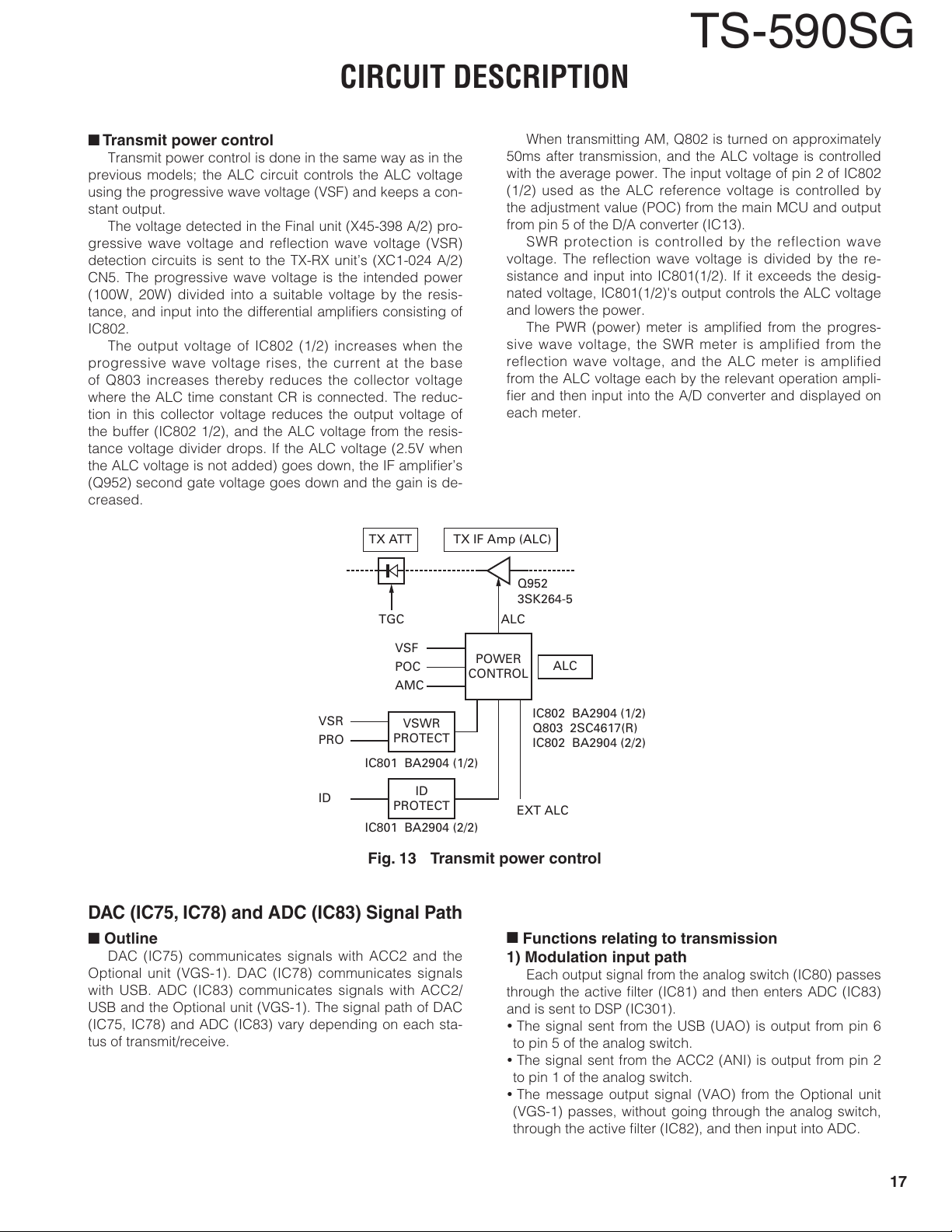
Transmit power control
Transmit power control is done in the same way as in the
previous models; the ALC circuit controls the ALC voltage
using the progressive wave voltage (VSF) and keeps a con-
stant output.
The voltage detected in the Final unit (X45-398 A/2) pro-
gressive wave voltage and reflection wave voltage (VSR)
detection circuits is sent to the TX-RX unit’s (XC1-024 A/2)
CN5. The progressive wave voltage is the intended power
(100W, 20W) divided into a suitable voltage by the resis-
tance, and input into the differential amplifi ers consisting of
IC802.
The output voltage of IC802 (1/2) increases when the
progressive wave voltage rises, the current at the base
of Q803 increases thereby reduces the collector voltage
where the ALC time constant CR is connected. The reduc-
tion in this collector voltage reduces the output voltage of
the buffer (IC802 1/2), and the ALC voltage from the resis-
tance voltage divider drops. If the ALC voltage (2.5V when
the ALC voltage is not added) goes down, the IF amplifi er’s
(Q952) second gate voltage goes down and the gain is de-
creased.
TX ATT
TGC
TX IF Amp (ALC)
When transmitting AM, Q802 is turned on approximately
50ms after transmission, and the ALC voltage is controlled
with the average power. The input voltage of pin 2 of IC802
(1/2) used as the ALC reference voltage is controlled by
the adjustment value (POC) from the main MCU and output
from pin 5 of the D/A converter (IC13).
SWR protection is controlled by the reflection wave
voltage. The refl ection wave voltage is divided by the re-
sistance and input into IC801(1/2). If it exceeds the desig-
nated voltage, IC801(1/2)'s output controls the ALC voltage
and lowers the power.
The PWR (power) meter is amplifi ed from the progres-
sive wave voltage, the SWR meter is amplified from the
reflection wave voltage, and the ALC meter is amplified
from the ALC voltage each by the relevant operation ampli-
fi er and then input into the A/D converter and displayed on
each meter.
Q952
3SK264-5
ALC
VSF
POC
AMC
VSR
PRO
ID
VSWR
PROTECT
IC801 BA2904 (1/2)
ID
PROTECT
IC801 BA2904 (2/2)
Fig. 13 Transmit power control
DAC (IC75, IC78) and ADC (IC83) Signal Path
n
Outline
DAC (IC75) communicates signals with ACC2 and the
Optional unit (VGS-1). DAC (IC78) communicates signals
with USB. ADC (IC83) communicates signals with ACC2/
USB and the Optional unit (VGS-1). The signal path of DAC
(IC75, IC78) and ADC (IC83) vary depending on each sta-
tus of transmit/receive.
POWER
CONTROL
ALC
IC802 BA2904 (1/2)
Q803 2SC4617(R)
IC802 BA2904 (2/2)
EXT ALC
n
Functions relating to transmission
1) Modulation input path
Each output signal from the analog switch (IC80) passes
through the active fi lter (IC81) and then enters ADC (IC83)
and is sent to DSP (IC301).
The signal sent from the USB (UAO) is output from pin 6
to pin 5 of the analog switch.
The signal sent from the ACC2 (ANI) is output from pin 2
to pin 1 of the analog switch.
The message output signal (VAO) from the Optional unit
(VGS-1) passes, without going through the analog switch,
through the active fi lter (IC82), and then input into ADC.
17
TS-590SG
CIRCUIT DESCRIPTION
2) Modulation output path
The AF signal processed in DSP (IC301) is output as
analog in DAC (IC75, IC78) and then amplifi ed by the active
fi lter (IC73, IC76).
The signal that passed through the active fi lter (IC73) is
sent to ACC2 output signal (ANO).
The signal that passed through the active fi lter (IC76) is
sent to USB output signal (UAI).
3) Recoding a message
Signals input from the microphone are processed in
ADC (IC66), passed through DSP, and then enter DAC
(IC75).
The signals output from DAC (IC75) pin 11 are sent to
the Optional unit (VGS-1) and recorded.
n
Constant received audio recording function
1) Recording
A part of received audio signal is processed in ADC
(IC66), goes through DSP (IC301), and then enters DAC
(IC75). The signals output from DAC (IC75) pin 11 are sent
to the Optional unit (VGS-1) and recorded. The recording
level is automatically compensated to become constant and
you cannot randomly change the level.
2) Playback
The output signal (VAO) from the Optional unit (VGS-1) is
input into ADC (IC83), goes through DSP (IC301), and out-
put as AF from DAC (IC72). Playback volume is controlled
by DSP.
n
Other functions
1) Playing a message (monitor)
The output signal (VAO) from the Optional unit (VGS-1)
is input into ADC (IC83), goes through DSP (IC301), and
output as AF from DAC (IC72). Playback audio is controlled
by DSP.
2) Playing a pre-recorded voice message
The above-mentioned signal path is also used for play-
ing a pre-recorded voice message.
Digital Control Circuit
n
Outline
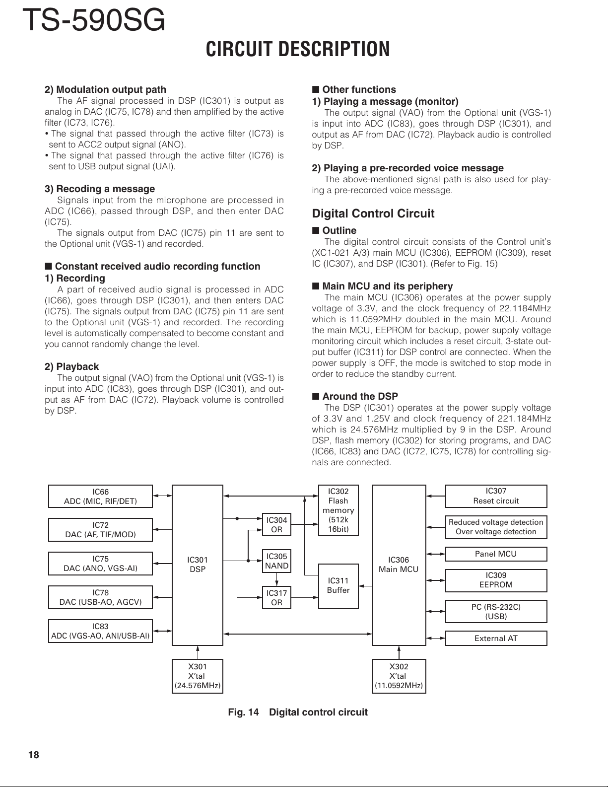
The digital control circuit consists of the Control unit’s
(XC1-021 A/3) main MCU (IC306), EEPROM (IC309), reset
IC (IC307), and DSP (IC301). (Refer to Fig. 15)
n
Main MCU and its periphery
The main MCU (IC306) operates at the power supply
voltage of 3.3V, and the clock frequency of 22.1184MHz
which is 11.0592MHz doubled in the main MCU. Around
the main MCU, EEPROM for backup, power supply voltage
monitoring circuit which includes a reset circuit, 3-state out-
put buffer (IC311) for DSP control are connected. When the
power supply is OFF, the mode is switched to stop mode in
order to reduce the standby current.
n
Around the DSP
The DSP (IC301) operates at the power supply voltage
of 3.3V and 1.25V and clock frequency of 221.184MHz
which is 24.576MHz multiplied by 9 in the DSP. Around
DSP, fl ash memory (IC302) for storing programs, and DAC
(IC66, IC83) and DAC (IC72, IC75, IC78) for controlling sig-
nals are connected.
IC66
ADC (MIC, RIF/DET)
IC72
DAC (AF, TIF/MOD)
IC75
DAC (ANO, VGS-AI)
IC78
DAC (USB-AO, AGCV)
IC83
ADC (VGS-AO, ANI/USB-AI)
18
IC301
DSP
X301
X’tal
(24.576MHz)
IC302
Flash
memory
IC304
OR
IC305
NAND
IC317
OR
(512k
16bit)
IC311
Buffer
Fig. 14 Digital control circuit
IC306
Main MCU
X302
X’tal
(11.0592MHz)
IC307
Reset circuit
Reduced voltage detection
Over voltage detection
Panel MCU
IC309
EEPROM
PC (RS-232C)
(USB)
External AT
CIRCUIT DESCRIPTION
Display Circuit
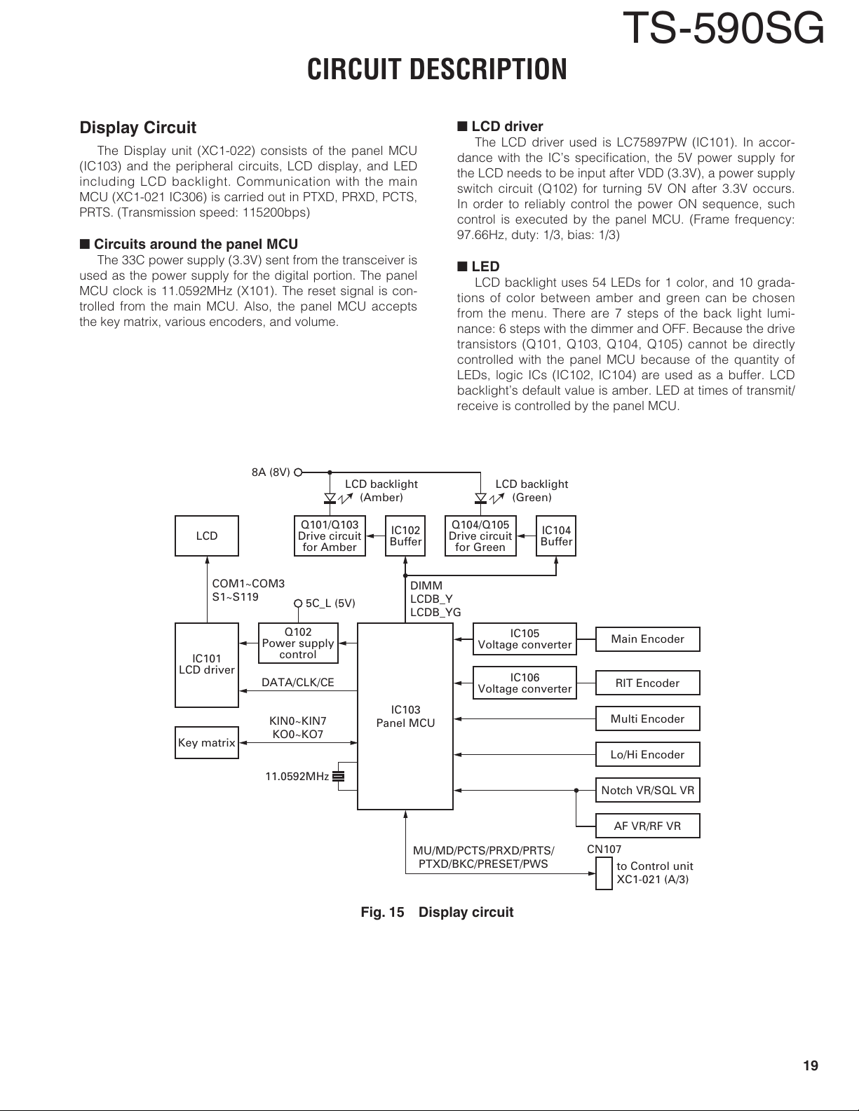
The Display unit (XC1-022) consists of the panel MCU
(IC103) and the peripheral circuits, LCD display, and LED
including LCD backlight. Communication with the main
MCU (XC1-021 IC306) is carried out in PTXD, PRXD, PCTS,
PRTS. (Transmission speed: 115200bps)
n
Circuits around the panel MCU
The 33C power supply (3.3V) sent from the transceiver is
used as the power supply for the digital portion. The panel
MCU clock is 11.0592MHz (X101). The reset signal is con-
trolled from the main MCU. Also, the panel MCU accepts
the key matrix, various encoders, and volume.
TS-590SG
n
LCD driver
The LCD driver used is LC75897PW (IC101). In accor-
dance with the IC’s specifi cation, the 5V power supply for
the LCD needs to be input after VDD (3.3V), a power supply
switch circuit (Q102) for turning 5V ON after 3.3V occurs.
In order to reliably control the power ON sequence, such
control is executed by the panel MCU. (Frame frequency:
97.66Hz, duty: 1/3, bias: 1/3)
n
LED
LCD backlight uses 54 LEDs for 1 color, and 10 grada-
tions of color between amber and green can be chosen
from the menu. There are 7 steps of the back light lumi-
nance: 6 steps with the dimmer and OFF. Because the drive
transistors (Q101, Q103, Q104, Q105) cannot be directly
controlled with the panel MCU because of the quantity of
LEDs, logic ICs (IC102, IC104) are used as a buffer. LCD
backlight’s default value is amber. LED at times of transmit/
receive is controlled by the panel MCU.
LCD
COM1~COM3
S1~S119
IC101
LCD driver
Key matrix
8A (8V)
Q101/Q103
Drive circuit
for Amber
Q102
Power supply
control
DATA/CLK/CE
KIN0~KIN7
KO0~KO7
11.0592MHz
5C_L (5V)
LCD backlight
(Amber)
IC102
Buffer
IC103
Panel MCU
LCD backlight
(Green)
Q104/Q105
Drive circuit
for Green
DIMM
LCDB_Y
LCDB_YG
IC105
Voltage converter
IC106
Voltage converter
MU/MD/PCTS/PRXD/PRTS/
PTXD/BKC/PRESET/PWS
IC104
Buffer
Main Encoder
RIT Encoder
Multi Encoder
Lo/Hi Encoder
Notch VR/SQL VR
AF VR/RF VR
CN107
to Control unit
XC1-021 (A/3)
Fig. 15 Display circuit
19
TS-590SG
COMPONENTS DESCRIPTION
Final unit (X45-398X-XX)
Ref. No. Use / Function
IC1 Shift register BPF switching
IC2,3 Inverter gate PHD detection
IC4
IC5 Comparator AMD detection
IC6 D-type fl ip-fl op PHD detection
IC7 Shift register
IC8~10 Shift register AT control
Q1
Q2
Q3,4 Final amplifi er Push-pull amplifi er
Q5 Switching Power supply control of 14S
Q101 Switching Over voltage detection
Q251,252 Amplifi er VSF signal amplifi er
Q253,254 Switching Relay (K46) control
Q501~Q508,
Q522
Q509,510 Switching FAN control
Q511 Switching Power supply control of 14S
Q513 Switching AT control
Q514,515 Switching Relay (K45) control
Q516 Switching FAN control
Q517,518 Switching AT control
Q519 Switching Relay (K44) control
Q520 Switching FAN control
Q521 ,Q523,
Q524
Q525,526 Switching
Q527~544
D1,2 Attenuator RF power control
D51,52 Protection Surge protection
D101 Protection Reverse connection protection
D102~110
D111 Protection Over voltage protection
D251~253
D254 Protection Surge protection
D255 Detection RF power detection
D256,257 Protection Surge protection
D258 Switch
D301~325
D501~503
Drain current
detection
Pre-drive amplifi er
Drive amplifi er
Switching
Switching AT control
Switching AT control
Reverse voltage
prevention
Detection RF power detection
Protection Surge protection
Protection Surge protection
Operation / Condition / Compatibility
Current detection
Q1: AT switching
Q2: ANT switching
Q4: BPF switching
Q5: FAN control
Q6: FAN control
Q8: AT control
Single amplifi er
Single amplifi er
Filter switching depending on
band
AT relay operation stops when
power is ON
Surge protection
Control unit (XC1-021X-XX)
Ref. No. Use / Function
IC1
IC2
IC3 8V AVR
IC4 3.3V AVR
IC5 5V AVR
IC6 1.25V AVR
IC61 OP amplifi er Isolation amplifi er for MIC signal
IC62,63 OP amplifi er Active fi lter for MIC signal
IC64,65 OP amplifi er Active fi lter for RIF signal
IC66 A/D converter
IC67 AF amplifi er
IC68 Analog switch
IC69 OP amplifi er Active fi lter for AF signal
IC70 OP amplifi er
IC71 OP amplifi er
IC72 D/A converter
IC73 OP amplifi er Active fi lter for ANO signal
IC74 OP amplifi er Active fi lter for VAI signal
IC75 D/A converter
IC76 OP amplifi er Active fi lter for UAI signal
IC77 OP amplifi er
IC78 D/A converter
IC79 OP amplifi er Active fi lter for AN1 signal
IC80 Analog switch ANI and UAO signal switch
IC81 OP amplifi er
IC82 OP amplifi er Active fi lter for VAO signal
IC83 A/D converter
IC301 DSP Digital signal
IC302 Flash memory Program for DSP
IC304 OR gate IC FCS control
IC305 NAND gate IC Inverter for A (23) signal
IC306 MCU Main microcomputer
IC307 Reset IC MCU reset signal
3.3V switching
regulator
8V switching
regulator
Operation / Condition / Compatibility
3.3V switching regulator
(Digital circuit)
8V switching regulator
(Analog circuit for TX-RX, Display
and Control unit)
8V voltage regulator
(Local unit XC1-021 B/3)
3.3V voltage regulator
(Main MCU and RS-232C circuit)
5V voltage regulator
(Analog circuit)
1.25V voltage regulator power
supply (DSP)
A/D converter for MIC and RIF
signal
FMOD and TIF signal ON/OFF
switch
Active fi lter for FMOD and TIF
signal
Active fi lter for FMOD, TIF and AF
signal
D/A converter for FMOD, TIF and
AF signal
D/A converter for ANO and VAI
signal
Buffer for AGCV signal and refer-
ence voltage source
D/A converter for UAI and AGCV
signal
Active fi lter for ANI and UAO
signal
A/D converter for ANI, UAO and
VAO signal
20
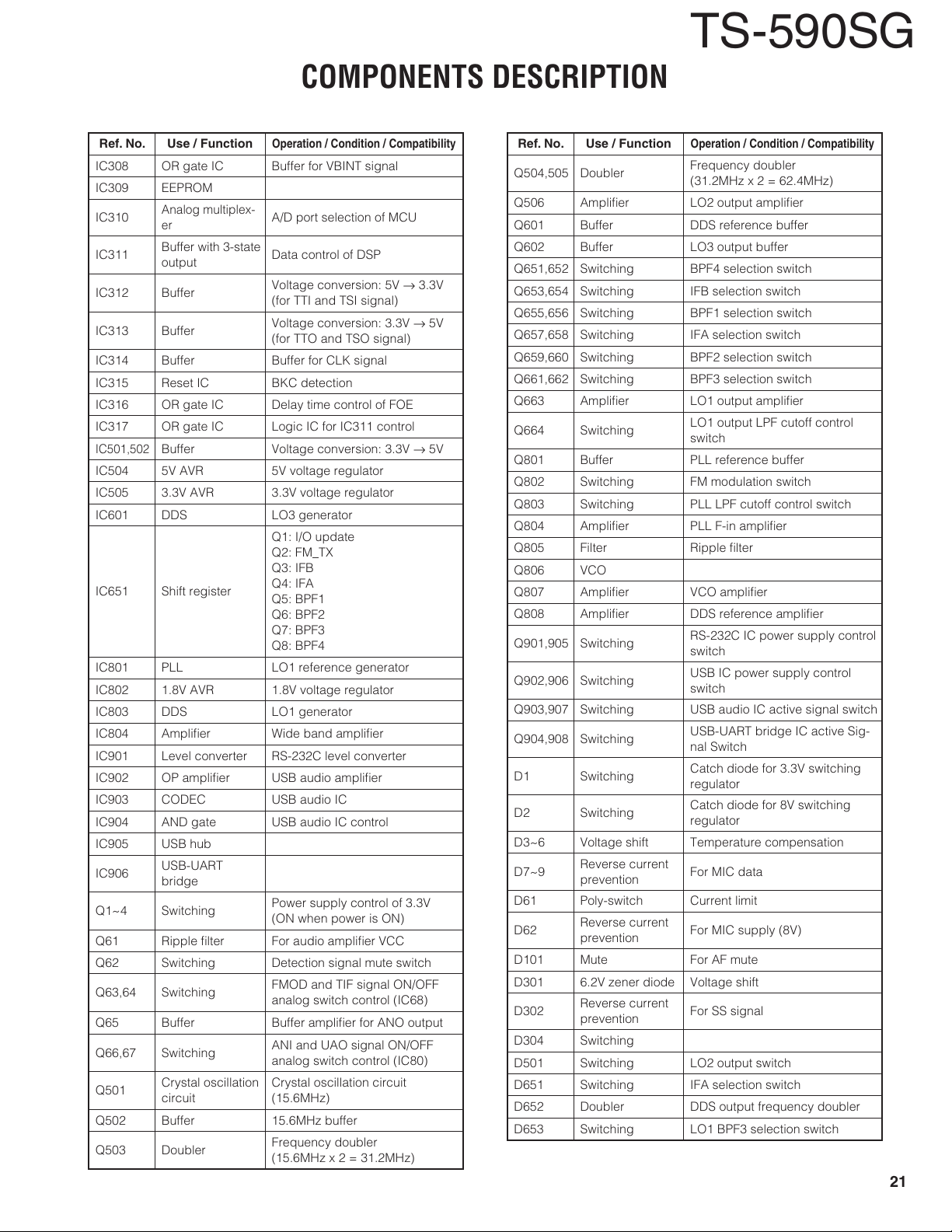
COMPONENTS DESCRIPTION
TS-590SG
Ref. No. Use / Function
IC308 OR gate IC Buffer for VBINT signal
IC309 EEPROM
IC310
IC311
IC312 Buffer
IC313 Buffer
IC314 Buffer Buffer for CLK signal
IC315 Reset IC BKC detection
IC316 OR gate IC Delay time control of FOE
IC317 OR gate IC Logic IC for IC311 control
IC501,502
IC504 5V AVR 5V voltage regulator
IC505 3.3V AVR 3.3V voltage regulator
IC601 DDS LO3 generator
IC651 Shift register
IC801 PLL LO1 reference generator
IC802 1.8V AVR 1.8V voltage regulator
IC803 DDS LO1 generator
IC804 Amplifi er Wide band amplifi er
IC901 Level converter RS-232C level converter
IC902 OP amplifi er USB audio amplifi er
IC903 CODEC USB audio IC
IC904 AND gate USB audio IC control
IC905 USB hub
IC906
Q1~4 Switching
Q61 Ripple fi lter For audio amplifi er VCC
Q62 Switching Detection signal mute switch
Q63,64 Switching
Q65 Buffer Buffer amplifi er for ANO output
Q66,67 Switching
Q501
Q502 Buffer 15.6MHz buffer
Q503 Doubler
Analog multiplex-
er
Buffer with 3-state
output
Buffer Voltage conversion: 3.3V → 5V
USB-UART
bridge
Crystal oscillation
circuit
Operation / Condition / Compatibility
A/D port selection of MCU
Data control of DSP
Voltage conversion: 5V → 3.3V
(for TTI and TSI signal)
Voltage conversion: 3.3V → 5V
(for TTO and TSO signal)
Q1: I/O update
Q2: FM_TX
Q3: IFB
Q4: IFA
Q5: BPF1
Q6: BPF2
Q7: BPF3
Q8: BPF4
Power supply control of 3.3V
(ON when power is ON)
FMOD and TIF signal ON/OFF
analog switch control (IC68)
ANI and UAO signal ON/OFF
analog switch control (IC80)
Crystal oscillation circuit
(15.6MHz)
Frequency doubler
(15.6MHz x 2 = 31.2MHz)
Ref. No. Use / Function
Q504,505 Doubler
Q506 Amplifi er LO2 output amplifi er
Q601 Buffer DDS reference buffer
Q602 Buffer LO3 output buffer
Q651,652 Switching BPF4 selection switch
Q653,654 Switching IFB selection switch
Q655,656 Switching BPF1 selection switch
Q657,658 Switching IFA selection switch
Q659,660 Switching BPF2 selection switch
Q661,662 Switching BPF3 selection switch
Q663 Amplifi er LO1 output amplifi er
Q664 Switching
Q801 Buffer PLL reference buffer
Q802 Switching FM modulation switch
Q803 Switching PLL LPF cutoff control switch
Q804 Amplifi er PLL F-in amplifi er
Q805 Filter Ripple fi lter
Q806 VCO
Q807 Amplifi er VCO amplifi er
Q808 Amplifi er DDS reference amplifi er
Q901,905 Switching
Q902,906 Switching
Q903,907 Switching USB audio IC active signal switch
Q904,908 Switching
D1 Switching
D2 Switching
D3~6 Voltage shift Temperature compensation
D7~9
D61 Poly-switch Current limit
D62
D101 Mute For AF mute
D301 6.2V zener diode Voltage shift
D302
D304 Switching
D501 Switching LO2 output switch
D651 Switching IFA selection switch
D652 Doubler DDS output frequency doubler
D653 Switching LO1 BPF3 selection switch
Reverse current
prevention
Reverse current
prevention
Reverse current
prevention
Operation / Condition / Compatibility
Frequency doubler
(31.2MHz x 2 = 62.4MHz)
LO1 output LPF cutoff control
switch
RS-232C IC power supply control
switch
USB IC power supply control
switch
USB-UART bridge IC active Sig-
nal Switch
Catch diode for 3.3V switching
regulator
Catch diode for 8V switching
regulator
For MIC data
For MIC supply (8V)
For SS signal
21
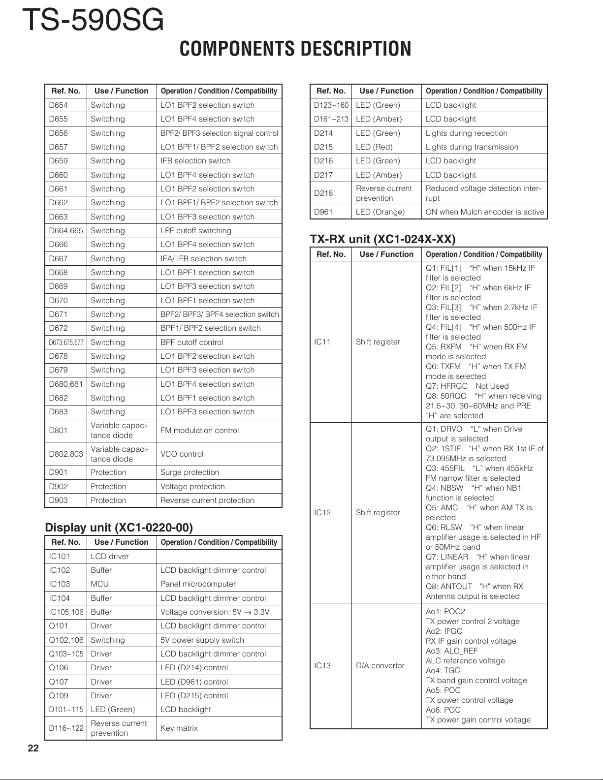
TS-590SG
COMPONENTS DESCRIPTION
Ref. No. Use / Function
D654 Switching LO1 BPF2 selection switch
D655 Switching LO1 BPF4 selection switch
D656 Switching
D657 Switching LO1 BPF1/ BPF2 selection switch
D659 Switching IFB selection switch
D660 Switching LO1 BPF4 selection switch
D661 Switching LO1 BPF2 selection switch
D662 Switching LO1 BPF1/ BPF2 selection switch
D663 Switching LO1 BPF3 selection switch
D664,665 Switching LPF cutoff switching
D666 Switching LO1 BPF4 selection switch
D667 Switching IFA/ IFB selection switch
D668 Switching LO1 BPF1 selection switch
D669 Switching LO1 BPF3 selection switch
D670 Switching LO1 BPF1 selection switch
D671 Switching
D672 Switching BPF1/ BPF2 selection switch
D673,675,677
D678 Switching LO1 BPF2 selection switch
D679 Switching LO1 BPF3 selection switch
D680,681 Switching LO1 BPF4 selection switch
D682 Switching LO1 BPF1 selection switch
D683 Switching LO1 BPF3 selection switch
D801
D802,803
D901 Protection Surge protection
D902 Protection Voltage protection
D903 Protection Reverse current protection
Switching BPF cutoff control
Variable capaci-
tance diode
Variable capaci-
tance diode
Operation / Condition / Compatibility
BPF2/ BPF3 selection signal control
BPF2/ BPF3/ BPF4 selection switch
FM modulation control
VCO control
Display unit (XC1-0220-00)
Ref. No. Use / Function
IC101 LCD driver
IC102 Buffer LCD backlight dimmer control
IC103 MCU Panel microcomputer
IC104 Buffer LCD backlight dimmer control
IC105,106
Q101 Driver LCD backlight dimmer control
Q102,106 Switching 5V power supply switch
Q103~105
Q106 Driver LED (D214) control
Q107 Driver LED (D961) control
Q109 Driver LED (D215) control
D101~115
D116~122
Buffer Voltage conversion: 5V → 3.3V
Driver LCD backlight dimmer control
LED (Green) LCD backlight
Reverse current
prevention
22
Operation / Condition / Compatibility
Key matrix
Ref. No. Use / Function
D123~160
D161~213
D214 LED (Green) Lights during reception
D215 LED (Red) Lights during transmission
D216 LED (Green) LCD backlight
D217 LED (Amber) LCD backlight
D218
D961 LED (Orange) ON when Mulch encoder is active
LED (Green) LCD backlight
LED (Amber) LCD backlight
Reverse current
prevention
Operation / Condition / Compatibility
Reduced voltage detection inter-
rupt
TX-RX unit (XC1-024X-XX)
Ref. No. Use / Function
IC11 Shift register
IC12 Shift register
IC13 D/A convertor
Operation / Condition / Compatibility
Q1: FIL[1] “H” when 15kHz IF
fi lter is selected
Q2: FIL[2] “H” when 6kHz IF
fi lter is selected
Q3: FIL[3] “H” when 2.7kHz IF
fi lter is selected
Q4: FIL[4] “H” when 500Hz IF
fi lter is selected
Q5: RXFM “H” when RX FM
mode is selected
Q6: TXFM “H” when TX FM
mode is selected
Q7: HFRGC Not Used
Q8: 50RGC “H” when receiving
21.5~30, 30~60MHz and PRE
”H” are selected
Q1: DRVO “L” when Drive
output is selected
Q2: 1STIF “H” when RX 1st IF of
73.095MHz is selected
Q3: 455FIL “L” when 455kHz
FM narrow fi lter is selected
Q4: NBSW “H” when NB1
function is selected
Q5: AMC “H” when AM TX is
selected
Q6: RLSW “H” when linear
amplifi er usage is selected in HF
or 50MHz band
Q7: LINEAR “H” when linear
amplifi er usage is selected in
either band
Q8: ANTOUT "H" when RX
Antenna output is selected
Ao1: POC2
TX power control 2 voltage
Ao2: IFGC
RX IF gain control voltage
Ao3: ALC_REF
ALC reference voltage
Ao4: TGC
TX band gain control voltage
Ao5: POC
TX power control voltage
Ao6: PGC
TX power gain control voltage
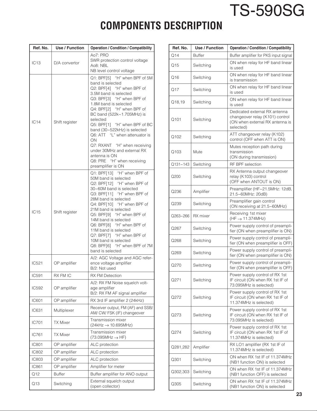
COMPONENTS DESCRIPTION
TS-590SG
Ref. No. Use / Function
IC13 D/A convertor
IC14 Shift register
IC15 Shift register
IC521 OP amplifi er
IC591 RX FM IC RX FM Detection
IC592 OP amplifi er
IC601 OP amplifi er RX 3rd IF amplifi er 2 (24kHz)
IC631 Multiplexer
IC701 TX Mixer
IC761 TX Mixer
IC801 OP amplifi er ALC protection
IC802 OP amplifi er ALC protection
IC803 OP amplifi er ALC protection
IC861 OP amplifi er Amplifi er for meter
Q12 Buffer Buffer amplifi er for ANO output
Q13 Switching
Operation / Condition / Compatibility
Ao7: PRO
SWR protection control voltage
Ao8: NBL
NB level control voltage
Q1: BPF[5] “H” when BPF of 5M
band is selected
Q2: BPF[4] “H” when BPF of
3.5M band is selected
Q3: BPF[3] “H” when BPF of
1.8M band is selected
Q4: BPF[2] “H” when BPF of
BC band (522k~1.705MHz) is
selected
Q5: BPF[1] “H” when BPF of BC
band (30~522kHz) is selected
Q6: ATT “L” when attenuator is
ON
Q7: RXANT “H” when receiving
under 30MHz and external RX
antenna is ON
Q8: PRE “H” when receiving
preamplifi er is ON
Q1: BPF[13] “H” when BPF of
50M band is selected
Q2: BPF[12] “H” when BPF of
30~60M band is selected
Q3: BPF[11] “H” when BPF of
28M band is selected
Q4: BPF[10] “H” when BPF of
21M band is selected
Q5: BPF[9] “H” when BPF of
14M band is selected
Q6: BPF[8] “H” when BPF of
11M band is selected
Q7: BPF[7] “H” when BPF of
10M band is selected
Q8: BPF[6] “H” when BPF of 7M
band is selected
A/2: AGC Voltage and AGC refer-
ence voltage amplifi er
B/2: Not used
A/2: RX FM Noise squelch volt-
age amplifi er
B/2: RX FM AF signal amplifi er
Receiver output, FM (AF) and SSB/
AM/ CW/ FSK (IF) changeover
Transmission mixer
(24kHz → 10.695MHz)
Transmission mixer
(73.095MHz → HF)
External squelch output
(open collector)
Ref. No. Use / Function
Q14 Buffer
Q15 Switching
Q16 Switching
Q17 Switching
Q18,19 Switching
Q101 Switching
Q102 Switching
Q103 Mute
Q131~143
Q200
Q236 Amplifi er
Q239 Switching
Q263~266
Q267 Switching
Q268 Switching
Q269 Switching
Q270 Switching
Q271 Switching
Q272 Switching
Q273 Switching
Q274 Switching
Q281,282 Amplifi er
Q301 Switching
Q302,303 Switching
Q305 Switching
Switching RF BPF selection
Switching
RX mixer
Operation / Condition / Compatibility
Buffer amplifi er for PKS input signal
ON when relay for HF band linear
is used
ON when relay for HF band linear
is transmission
ON when relay for HF band linear
is used
ON when relay for HF band linear
is used
Dedicated external RX antenna
changeover relay (K101) control
(ON when external RX antenna is
selected)
ATT changeover relay (K102)
control (OFF when ATT is ON)
Mutes reception path during
transmission
(ON during transmission)
RX Antenna output changeover
relay (K103) control
(OFF when ANTOUT is ON)
Preamplifi er (HF~21.5MHz: 12dB,
21.5~60MHz: 20dB)
Preamplifi er gain control
(ON receiving at 21.5~60MHz)
Receiving 1st mixer
(HF → 11.374MHz)
Power supply control of preampli-
fi er (ON when preamplifi er is ON)
Power supply control of preampli-
fi er (ON when preamplifi er is OFF)
Power supply control of preampli-
fi er (ON when preamplifi er is ON)
Power supply control of preampli-
fi er (ON when preamplifi er is OFF)
Power supply control of RX 1st
IF circuit (ON when RX 1st IF of
73.095MHz is selected)
Power supply control of RX 1st
IF circuit (ON when RX 1st IF of
11.374MHz is selected)
Power supply control of RX 1st
IF circuit (ON when RX 1st IF of
73.095MHz is selected)
Power supply control of RX 1st
IF circuit (ON when RX 1st IF of
11.374MHz is selected)
RX LO1 amplifi er (RX 1st IF of
11.374MHz is selected)
ON when RX 1st IF of 11.374MHz
(NB1 function ON) is selected
ON when RX 1st IF of 11.374MHz
(NB1 function OFF) is selected
ON when RX 1st IF of 11.374MHz
(NB1 function ON) is selected
23
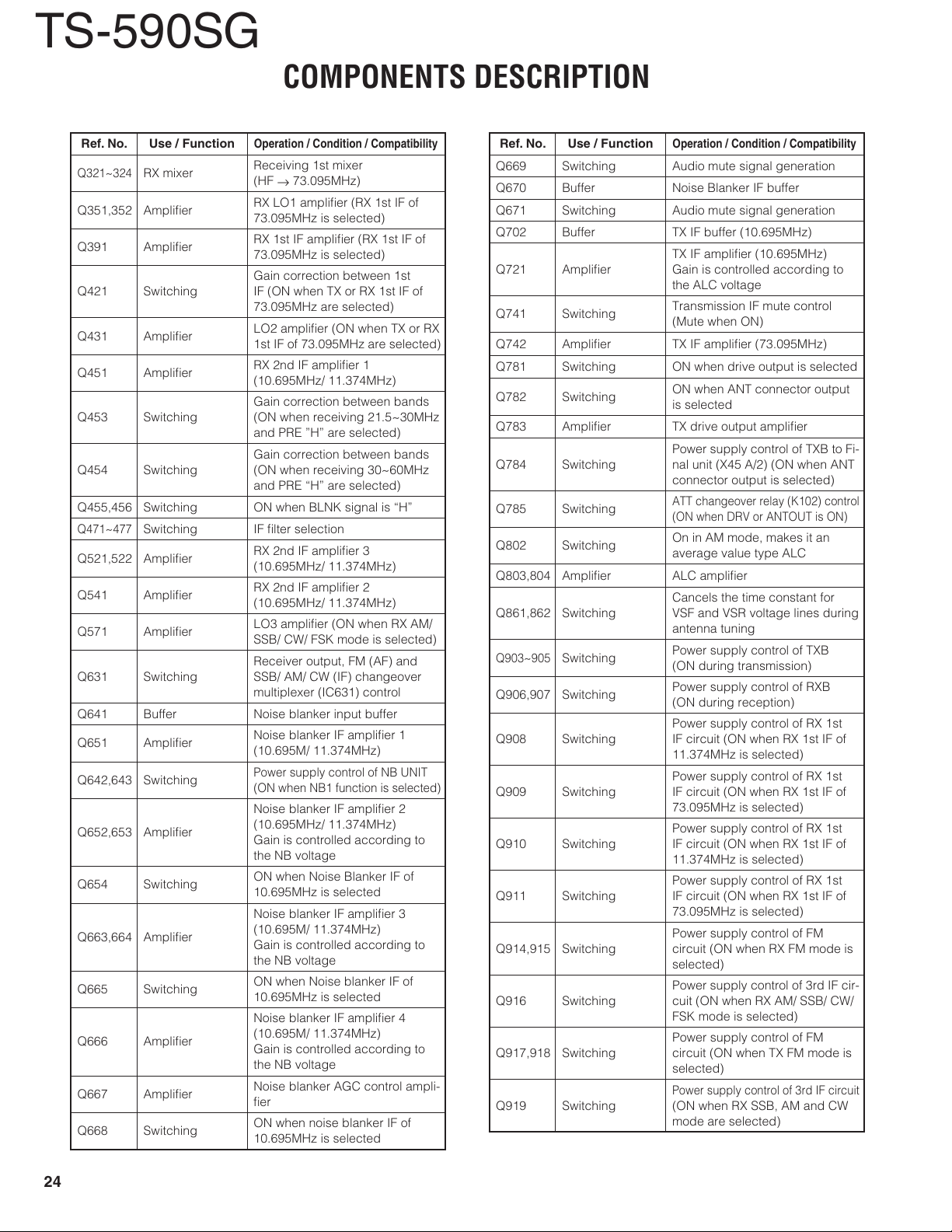
TS-590SG
COMPONENTS DESCRIPTION
Ref. No. Use / Function
Q321~324
Q351,352 Amplifi er
Q391 Amplifi er
Q421 Switching
Q431 Amplifi er
Q451 Amplifi er
Q453 Switching
Q454 Switching
Q455,456 Switching ON when BLNK signal is “H”
Q471~477
Q521,522 Amplifi er
Q541 Amplifi er
Q571 Amplifi er
Q631 Switching
Q641 Buffer Noise blanker input buffer
Q651 Amplifi er
Q642,643 Switching
Q652,653 Amplifi er
Q654 Switching
Q663,664 Amplifi er
Q665 Switching
Q666 Amplifi er
Q667 Amplifi er
Q668 Switching
RX mixer
Switching IF fi lter selection
Operation / Condition / Compatibility
Receiving 1st mixer
(HF → 73.095MHz)
RX LO1 amplifi er (RX 1st IF of
73.095MHz is selected)
RX 1st IF amplifi er (RX 1st IF of
73.095MHz is selected)
Gain correction between 1st
IF (ON when TX or RX 1st IF of
73.095MHz are selected)
LO2 amplifi er (ON when TX or RX
1st IF of 73.095MHz are selected)
RX 2nd IF amplifi er 1
(10.695MHz/ 11.374MHz)
Gain correction between bands
(ON when receiving 21.5~30MHz
and PRE ”H” are selected)
Gain correction between bands
(ON when receiving 30~60MHz
and PRE “H” are selected)
RX 2nd IF amplifi er 3
(10.695MHz/ 11.374MHz)
RX 2nd IF amplifi er 2
(10.695MHz/ 11.374MHz)
LO3 amplifi er (ON when RX AM/
SSB/ CW/ FSK mode is selected)
Receiver output, FM (AF) and
SSB/ AM/ CW (IF) changeover
multiplexer (IC631) control
Noise blanker IF amplifi er 1
(10.695M/ 11.374MHz)
Power supply control of NB UNIT
(ON when NB1 function is selected)
Noise blanker IF amplifi er 2
(10.695MHz/ 11.374MHz)
Gain is controlled according to
the NB voltage
ON when Noise Blanker IF of
10.695MHz is selected
Noise blanker IF amplifi er 3
(10.695M/ 11.374MHz)
Gain is controlled according to
the NB voltage
ON when Noise blanker IF of
10.695MHz is selected
Noise blanker IF amplifi er 4
(10.695M/ 11.374MHz)
Gain is controlled according to
the NB voltage
Noise blanker AGC control ampli-
fi e r
ON when noise blanker IF of
10.695MHz is selected
Ref. No. Use / Function
Q669 Switching Audio mute signal generation
Q670 Buffer Noise Blanker IF buffer
Q671 Switching Audio mute signal generation
Q702 Buffer TX IF buffer (10.695MHz)
Q721 Amplifi er
Q741 Switching
Q742 Amplifi er TX IF amplifi er (73.095MHz)
Q781 Switching ON when drive output is selected
Q782 Switching
Q783 Amplifi er TX drive output amplifi er
Q784 Switching
Q785 Switching
Q802 Switching
Q803,804 Amplifi er ALC amplifi er
Q861,862 Switching
Q903~905
Q906,907 Switching
Q908 Switching
Q909 Switching
Q910 Switching
Q911 Switching
Q914,915 Switching
Q916 Switching
Q917,918 Switching
Q919 Switching
Switching
Operation / Condition / Compatibility
TX IF amplifi er (10.695MHz)
Gain is controlled according to
the ALC voltage
Transmission IF mute control
(Mute when ON)
ON when ANT connector output
is selected
Power supply control of TXB to Fi-
nal unit (X45 A/2) (ON when ANT
connector output is selected)
ATT changeover relay (K102) control
(ON when DRV or ANTOUT is ON)
On in AM mode, makes it an
average value type ALC
Cancels the time constant for
VSF and VSR voltage lines during
antenna tuning
Power supply control of TXB
(ON during transmission)
Power supply control of RXB
(ON during reception)
Power supply control of RX 1st
IF circuit (ON when RX 1st IF of
11.374MHz is selected)
Power supply control of RX 1st
IF circuit (ON when RX 1st IF of
73.095MHz is selected)
Power supply control of RX 1st
IF circuit (ON when RX 1st IF of
11.374MHz is selected)
Power supply control of RX 1st
IF circuit (ON when RX 1st IF of
73.095MHz is selected)
Power supply control of FM
circuit (ON when RX FM mode is
selected)
Power supply control of 3rd IF cir-
cuit (ON when RX AM/ SSB/ CW/
FSK mode is selected)
Power supply control of FM
circuit (ON when TX FM mode is
selected)
Power supply control of 3rd IF circuit
(ON when RX SSB, AM and CW
mode are selected)
24
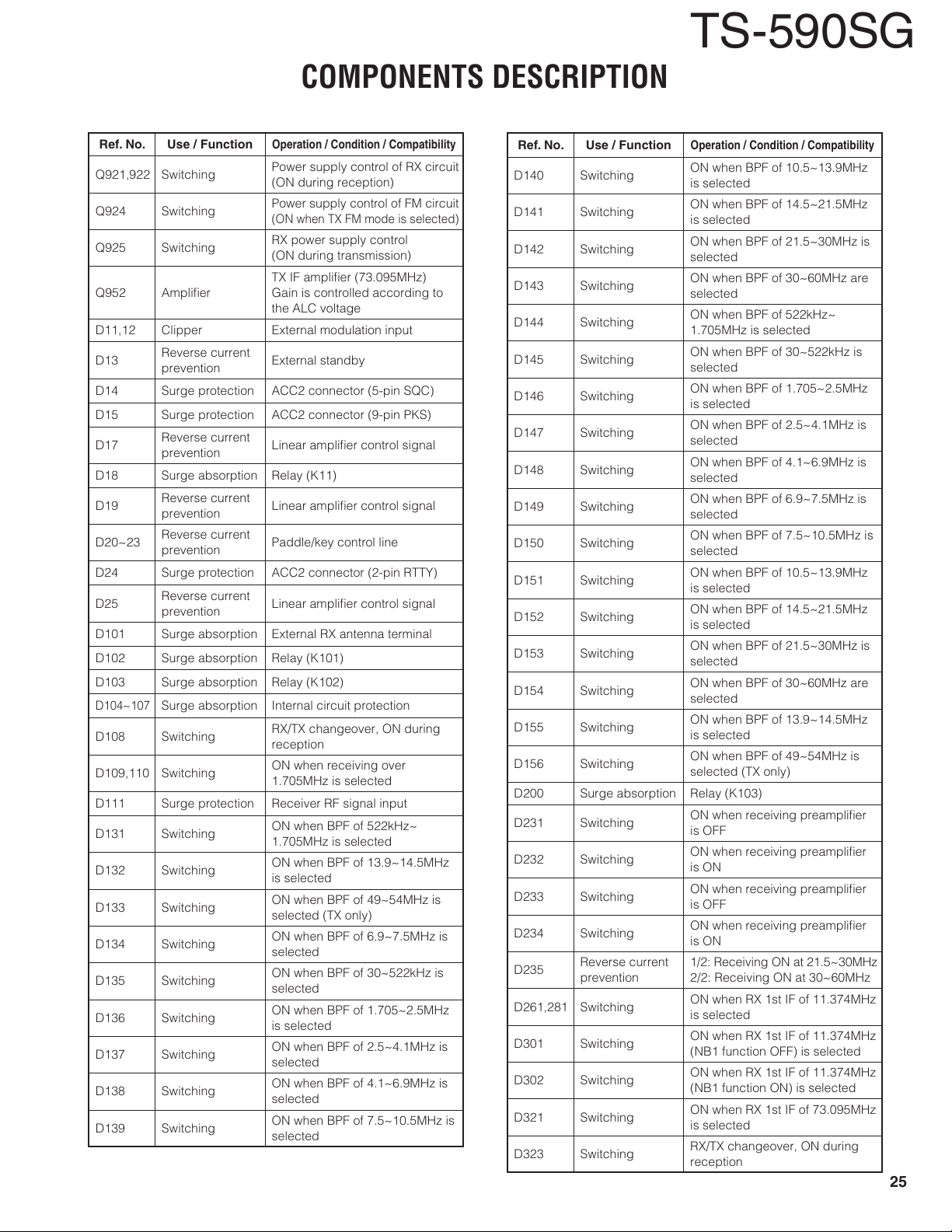
COMPONENTS DESCRIPTION
TS-590SG
Ref. No. Use / Function
Q921,922 Switching
Q924 Switching
Q925 Switching
Q952 Amplifi er
D11,12 Clipper External modulation input
D13
D14 Surge protection ACC2 connector (5-pin SQC)
D15 Surge protection ACC2 connector (9-pin PKS)
D17
D18 Surge absorption Relay (K11)
D19
D20~23
D24 Surge protection ACC2 connector (2-pin RTTY)
D25
D101 Surge absorption External RX antenna terminal
D102 Surge absorption Relay (K101)
D103 Surge absorption Relay (K102)
D104~107
D108 Switching
D109,110 Switching
D111 Surge protection Receiver RF signal input
D131 Switching
D132 Switching
D133 Switching
D134 Switching
D135 Switching
D136 Switching
D137 Switching
D138 Switching
D139 Switching
Reverse current
prevention
Reverse current
prevention
Reverse current
prevention
Reverse current
prevention
Reverse current
prevention
Surge absorption Internal circuit protection
Operation / Condition / Compatibility
Power supply control of RX circuit
(ON during reception)
Power supply control of FM circuit
(ON when TX FM mode is selected)
RX power supply control
(ON during transmission)
TX IF amplifi er (73.095MHz)
Gain is controlled according to
the ALC voltage
External standby
Linear amplifi er control signal
Linear amplifi er control signal
Paddle/key control line
Linear amplifi er control signal
RX/TX changeover, ON during
reception
ON when receiving over
1.705MHz is selected
ON when BPF of 522kHz~
1.705MHz is selected
ON when BPF of 13.9~14.5MHz
is selected
ON when BPF of 49~54MHz is
selected (TX only)
ON when BPF of 6.9~7.5MHz is
selected
ON when BPF of 30~522kHz is
selected
ON when BPF of 1.705~2.5MHz
is selected
ON when BPF of 2.5~4.1MHz is
selected
ON when BPF of 4.1~6.9MHz is
selected
ON when BPF of 7.5~10.5MHz is
selected
Ref. No. Use / Function
D140 Switching
D141 Switching
D142 Switching
D143 Switching
D144 Switching
D145 Switching
D146 Switching
D147 Switching
D148 Switching
D149 Switching
D150 Switching
D151 Switching
D152 Switching
D153 Switching
D154 Switching
D155 Switching
D156 Switching
D200 Surge absorption Relay (K103)
D231 Switching
D232 Switching
D233 Switching
D234 Switching
D235
D261,281 Switching
D301 Switching
D302 Switching
D321 Switching
D323 Switching
Reverse current
prevention
Operation / Condition / Compatibility
ON when BPF of 10.5~13.9MHz
is selected
ON when BPF of 14.5~21.5MHz
is selected
ON when BPF of 21.5~30MHz is
selected
ON when BPF of 30~60MHz are
selected
ON when BPF of 522kHz~
1.705MHz is selected
ON when BPF of 30~522kHz is
selected
ON when BPF of 1.705~2.5MHz
is selected
ON when BPF of 2.5~4.1MHz is
selected
ON when BPF of 4.1~6.9MHz is
selected
ON when BPF of 6.9~7.5MHz is
selected
ON when BPF of 7.5~10.5MHz is
selected
ON when BPF of 10.5~13.9MHz
is selected
ON when BPF of 14.5~21.5MHz
is selected
ON when BPF of 21.5~30MHz is
selected
ON when BPF of 30~60MHz are
selected
ON when BPF of 13.9~14.5MHz
is selected
ON when BPF of 49~54MHz is
selected (TX only)
ON when receiving preamplifi er
is OFF
ON when receiving preamplifi er
is ON
ON when receiving preamplifi er
is OFF
ON when receiving preamplifi er
is ON
1/2: Receiving ON at 21.5~30MHz
2/2: Receiving ON at 30~60MHz
ON when RX 1st IF of 11.374MHz
is selected
ON when RX 1st IF of 11.374MHz
(NB1 function OFF) is selected
ON when RX 1st IF of 11.374MHz
(NB1 function ON) is selected
ON when RX 1st IF of 73.095MHz
is selected
RX/TX changeover, ON during
reception
25
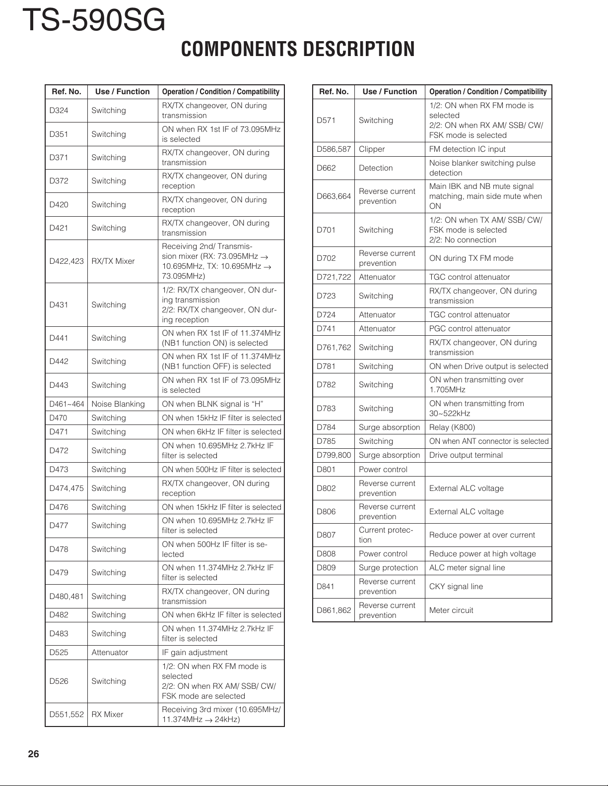
TS-590SG
COMPONENTS DESCRIPTION
Ref. No. Use / Function
D324 Switching
D351 Switching
D371 Switching
D372 Switching
D420 Switching
D421 Switching
D422,423 RX/TX Mixer
D431 Switching
D441 Switching
D442 Switching
D443 Switching
D461~464
D470
D471 Switching ON when 6kHz IF fi lter is selected
D472 Switching
D473 Switching
D474,475 Switching
D476 Switching
D477 Switching
D478 Switching
D479 Switching
D480,481 Switching
D482 Switching ON when 6kHz IF fi lter is selected
D483 Switching
D525 Attenuator IF gain adjustment
D526 Switching
D551,552 RX Mixer
Noise Blanking ON when BLNK signal is “H”
Switching
Operation / Condition / Compatibility
RX/TX changeover, ON during
transmission
ON when RX 1st IF of 73.095MHz
is selected
RX/TX changeover, ON during
transmission
RX/TX changeover, ON during
reception
RX/TX changeover, ON during
reception
RX/TX changeover, ON during
transmission
Receiving 2nd/ Transmis-
sion mixer (RX: 73.095MHz →
10.695MHz, TX: 10.695MHz →
73.095MHz)
1/2: RX/TX changeover, ON dur-
ing transmission
2/2: RX/TX changeover, ON dur-
ing reception
ON when RX 1st IF of 11.374MHz
(NB1 function ON) is selected
ON when RX 1st IF of 11.374MHz
(NB1 function OFF) is selected
ON when RX 1st IF of 73.095MHz
is selected
ON when 15kHz IF fi lter is selected
ON when 10.695MHz 2.7kHz IF
fi lter is selected
ON when 500Hz IF fi lter is selected
RX/TX changeover, ON during
reception
ON when 15kHz IF fi lter is selected
ON when 10.695MHz 2.7kHz IF
fi lter is selected
ON when 500Hz IF fi lter is se-
lected
ON when 11.374MHz 2.7kHz IF
fi lter is selected
RX/TX changeover, ON during
transmission
ON when 11.374MHz 2.7kHz IF
fi lter is selected
1/2: ON when RX FM mode is
selected
2/2: ON when RX AM/ SSB/ CW/
FSK mode are selected
Receiving 3rd mixer (10.695MHz/
11.374MHz → 24kHz)
Ref. No. Use / Function
D571 Switching
D586,587 Clipper FM detection IC input
D662 Detection
D663,664
D701 Switching
D702
D721,722 Attenuator TGC control attenuator
D723 Switching
D724
D741 Attenuator PGC control attenuator
D761,762 Switching
D781 Switching ON when Drive output is selected
D782 Switching
D783 Switching
D784 Surge absorption Relay (K800)
D785 Switching
D799,800 Surge absorption Drive output terminal
D801 Power control
D802
D806
D807
D808 Power control Reduce power at high voltage
D809 Surge protection ALC meter signal line
D841
D861,862
Reverse current
prevention
Reverse current
prevention
Attenuator TGC control attenuator
Reverse current
prevention
Reverse current
prevention
Current protec-
tion
Reverse current
prevention
Reverse current
prevention
Operation / Condition / Compatibility
1/2: ON when RX FM mode is
selected
2/2: ON when RX AM/ SSB/ CW/
FSK mode is selected
Noise blanker switching pulse
detection
Main IBK and NB mute signal
matching, main side mute when
ON
1/2: ON when TX AM/ SSB/ CW/
FSK mode is selected
2/2: No connection
ON during TX FM mode
RX/TX changeover, ON during
transmission
RX/TX changeover, ON during
transmission
ON when transmitting over
1.705MHz
ON when transmitting from
30~522kHz
ON when ANT connector is selected
External ALC voltage
External ALC voltage
Reduce power at over current
CKY signal line
Meter circuit
26
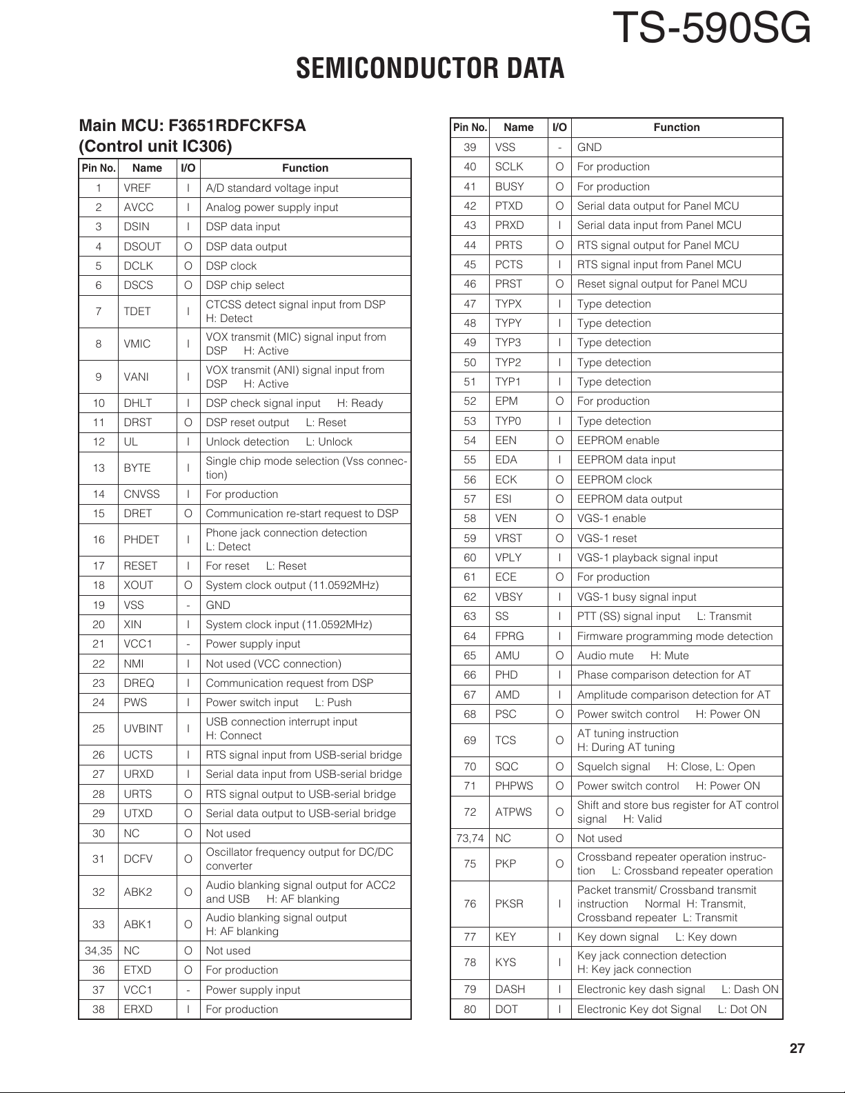
SEMICONDUCTOR DATA
TS-590SG
Main MCU: F3651RDFCKFSA (Control unit IC306)
Pin No.
34,35 NC O Not used
Name I/O Function
1 VREF I A/D standard voltage input
2 AVCC I Analog power supply input
3 DSIN I DSP data input
4 DSOUT O DSP data output
5 DCLK O DSP clock
6 DSCS O DSP chip select
7 TDET I
8 VMIC I
9 VANI I
10 DHLT I DSP check signal input H: Ready
11 DRST O DSP reset output L: Reset
12 UL I Unlock detection L: Unlock
13 BYTE I
14 CNVSS I For production
15 DRET O Communication re-start request to DSP
16 PHDET I
17 RESET I For reset L: Reset
18 XOUT O System clock output (11.0592MHz)
19 VSS - GND
20 XIN I System clock input (11.0592MHz)
21 VCC1 - Power supply input
22 NMI I Not used (VCC connection)
23 DREQ I Communication request from DSP
24 PWS I Power switch input L: Push
25 UVBINT I
26 UCTS I RTS signal input from USB-serial bridge
27 URXD I Serial data input from USB-serial bridge
28 URTS O RTS signal output to USB-serial bridge
29 UTXD O Serial data output to USB-serial bridge
30 NC O Not used
31 DCFV O
32 ABK2 O
33 ABK1 O
36 ETXD O For production
37 VCC1 - Power supply input
38 ERXD I For production
CTCSS detect signal input from DSP
H: Detect
VOX transmit (MIC) signal input from
DSP H: Active
VOX transmit (ANI) signal input from
DSP H: Active
Single chip mode selection (Vss connec-
tion)
Phone jack connection detection
L: Detect
USB connection interrupt input
H: Connect
Oscillator frequency output for DC/DC
converter
Audio blanking signal output for ACC2
and USB H: AF blanking
Audio blanking signal output
H: AF blanking
Pin No.
73,74 NC O Not used
Name I/O Function
39 VSS - GND
40 SCLK O For production
41 BUSY O For production
42 PTXD O Serial data output for Panel MCU
43 PRXD I Serial data input from Panel MCU
44 PRTS O RTS signal output for Panel MCU
45 PCTS I RTS signal input from Panel MCU
46 PRST O Reset signal output for Panel MCU
47 TYPX I Type detection
48 TYPY I Type detection
49 TYP3 I Type detection
50 TYP2 I Type detection
51 TYP1 I Type detection
52 EPM O For production
53 TYP0 I Type detection
54 EEN O EEPROM enable
55 EDA I EEPROM data input
56 ECK O EEPROM clock
57 ESI O EEPROM data output
58 VEN O VGS-1 enable
59 VRST O VGS-1 reset
60 VPLY I VGS-1 playback signal input
61 ECE O For production
62 VBSY I VGS-1 busy signal input
63 SS I PTT (SS) signal input L: Transmit
64 FPRG I Firmware programming mode detection
65 AMU O Audio mute H: Mute
66 PHD I Phase comparison detection for AT
67 AMD I Amplitude comparison detection for AT
68 PSC O Power switch control H: Power ON
69 TCS O
70 SQC O Squelch signal H: Close, L: Open
71 PHPWS O Power switch control H: Power ON
72 ATPWS O
75 PKP O
76 PKSR I
77 KEY I Key down signal L: Key down
78 KYS I
79 DASH I
80 DOT I Electronic Key dot Signal L: Dot ON
AT tuning instruction
H: During AT tuning
Shift and store bus register for AT control
signal H: Valid
Crossband repeater operation instruc-
tion L: Crossband repeater operation
Packet transmit/ Crossband transmit
instruction Normal H: Transmit,
Crossband repeater L: Transmit
Key jack connection detection
H: Key jack connection
Electronic key dash signal L: Dash ON
27
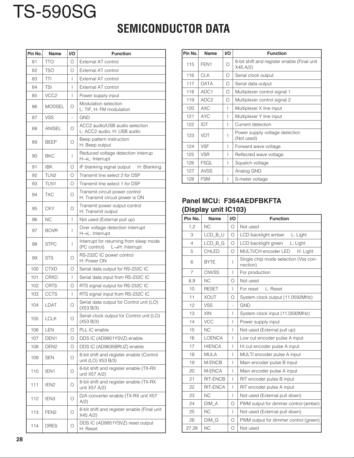
TS-590SG
SEMICONDUCTOR DATA
Pin No.
100 CTXD O Serial data output for RS-232C IC
101 CRXD I Serial data input from RS-232C IC
102 CRTS O RTS signal output for RS-232C IC
103 CCTS I RTS signal input from RS-232C IC
104 LDAT O
105 LCLK O
106 LEN O PLL IC enable
107 DEN1 O DDS IC (AD9951YSVZ) enable
108 DEN2 O DDS IC (AD9835BRUZ) enable
109 SEN O
110 IEN1 O
111 IEN2 O
112 IEN3 O
113 FEN2 O
114 DRES O
Name I/O Function
81 TTO O External AT control
82 TSO O External AT control
83 TTI I External AT control
84 TSI I External AT control
85 VCC2 I Power supply input
86 MODSEL O
87 VSS - GND
88 ANISEL O
89 BEEP O
90 BKC I
91 IBK O IF blanking signal output H: Blanking
92 TLN2 O Transmit line select 2 for DSP
93 TLN1 O Transmit line select 1 for DSP
94 TXC O
95 CKY O
96 NC I Not used (External pull up)
97 BOVR I
98 STPC I
99 STS O
Modulation selection
L: TIF, H: FM modulation
ACC2 audio/USB audio selection
L: ACC2 audio, H: USB audio
Beep pattern instruction
H: Beep output
Reduced voltage detection interrup
H→L: Interrupt
Transmit circuit power control
H: Transmit circuit power is ON
Transmit power output control
H: Transmit output
Over voltage detection interrupt
H→L: Interrupt
Interrupt for returning from sleep mode
(PC control) L→H: Interrupt
RS-232C IC power control
H: Power ON
Serial data output for Control unit (LO)
(X53 B/3)
Serial clock output for Control unit (LO)
(X53 B/3)
8-bit shift and register enable (Control
unit (LO) X53 B/3)
8-bit shift and register enable (TX-RX
unit X57 A/2)
8-bit shift and register enable (TX-RX
unit X57 A/2)
D/A converter enable (TX-RX unit X57
A/2)
8-bit shift and register enable (Final unit
X45 A/2)
DDS IC (AD9951YSVZ) reset output
H: Reset
Pin No.
115 FEN1 O
116 CLK O Serial clock output
117 DATA O Serial data output
118 ADC1 O Multiplexer control signal 1
119 ADC2 O Multiplexer control signal 2
120 AXC I Multiplexer X line input
121 AYC I Multiplexer Y line input
122 IDT I Current detection
123 VDT I
124 VSF I Forward wave voltage
125 VSR I Refl ected wave voltage
126 FSQL I Squelch voltage
127 AVSS - Analog GND
128 FSM I S-meter voltage
Name I/O Function
8-bit shift and register enable (Final unit
X45 A/2)
Power supply voltage detection
(Not used)
Panel MCU: F364AEDFBKFTA (Display unit IC103)
Pin No. Name I/O Function
1,2 NC O Not used
3 LCD_B_U O LCD backlight amber L: Light
4 LCD_B_G O LCD backlight green L: Light
5 CHLED O MULTI/CH encoder LED H: Light
6 BYTE I
7 CNVSS I For production
8,9 NC O Not used
10 RESET I For reset L: Reset
11 XOUT O System clock output (11.0592MHz)
12 VSS - GND
13 XIN I System clock input (11.0592MHz)
14 VCC I Power supply input
15 NC I Not used (External pull up)
16 LOENCA I Low cut encoder pulse A input
17 HIENCA I Hi cut encoder pulse A input
18 MULA I MULTI encoder pulse A input
19 M-ENCB I Main encoder pulse B input
20 M-ENCA I Main encoder pulse A input
21 RIT-ENCB I RIT encoder pulse B input
22 RIT-ENCA I RIT encoder pulse A input
23 NC I Not used (External pull down)
24 DIM_A O
25 NC I Not used (External pull down)
26 DIM_G O PWM output for dimmer control (green)
27,28 NC O Not used
Single chip mode selection (Vss con-
nection)
PWM output for dimmer control (amber)
28
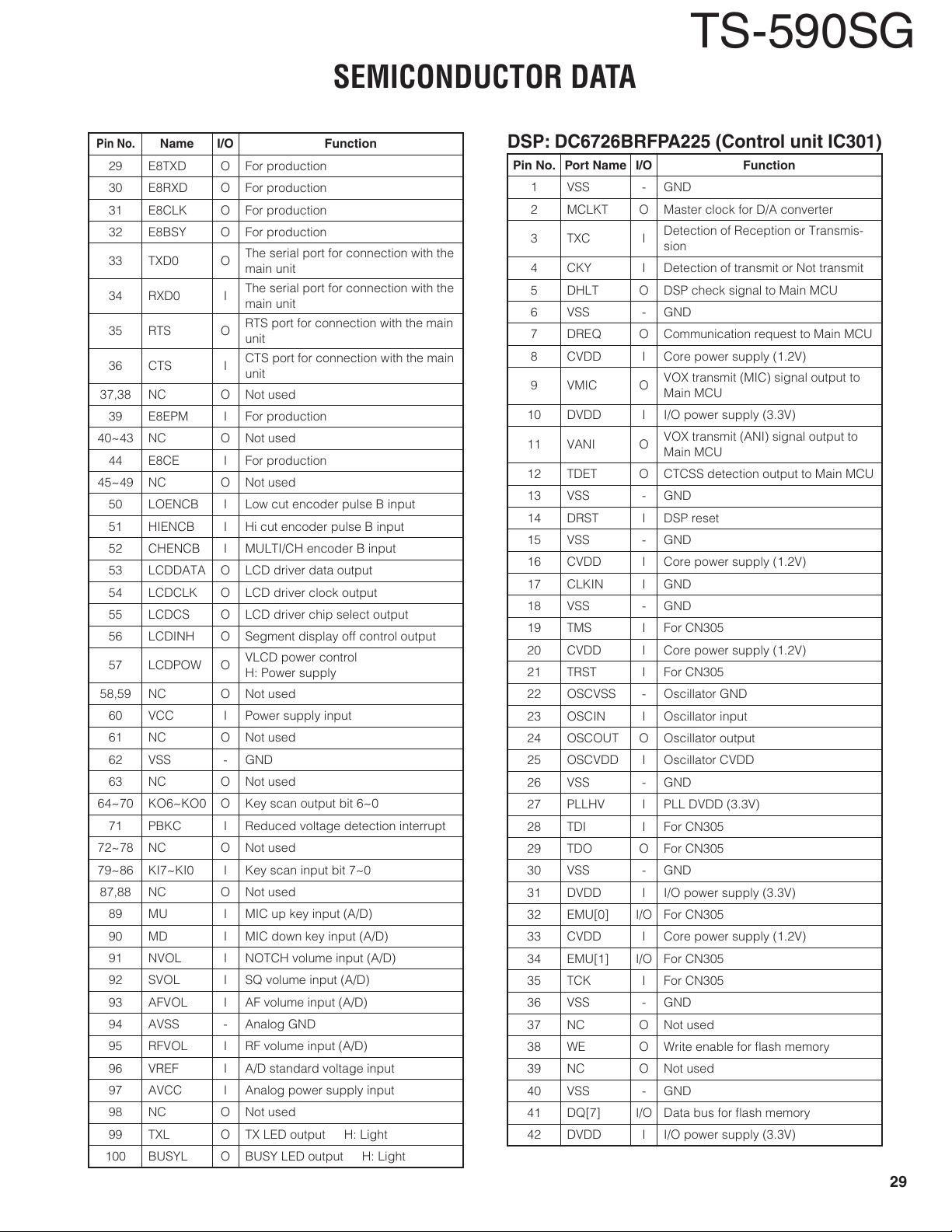
SEMICONDUCTOR DATA
TS-590SG
Pin No.
29 E8TXD O For production
30 E8RXD O For production
31 E8CLK O For production
32 E8BSY O For production
33 TXD0 O
34 RXD0 I
35 RTS O
36 CTS I
37,38 NC O Not used
39 E8EPM I For production
40~43 NC O Not used
44 E8CE I For production
45~49 NC O Not used
50 LOENCB I Low cut encoder pulse B input
51 HIENCB I Hi cut encoder pulse B input
52 CHENCB I MULTI/CH encoder B input
53 LCDDATA O LCD driver data output
54 LCDCLK O LCD driver clock output
55 LCDCS O LCD driver chip select output
56 LCDINH O Segment display off control output
57 LCDPOW O
58,59 NC O Not used
60 VCC I Power supply input
61 NC O Not used
62 VSS - GND
63 NC O Not used
64~70 KO6~KO0 O Key scan output bit 6~0
71 PBKC I Reduced voltage detection interrupt
72~78 NC O Not used
79~86 KI7~KI0 I Key scan input bit 7~0
87,88 NC O Not used
89 MU I MIC up key input (A/D)
90 MD I MIC down key input (A/D)
91 NVOL I NOTCH volume input (A/D)
92 SVOL I SQ volume input (A/D)
93 AFVOL I AF volume input (A/D)
94 AVSS - Analog GND
95 RFVOL I RF volume input (A/D)
96 VREF I A/D standard voltage input
97 AVCC I Analog power supply input
98 NC O Not used
99 TXL O TX LED output H: Light
100 BUSYL O BUSY LED output H: Light
Name I/O Function
The serial port for connection with the
main unit
The serial port for connection with the
main unit
RTS port for connection with the main
unit
CTS port for connection with the main
unit
VLCD power control
H: Power supply
DSP: DC6726BRFPA225 (Control unit IC301)
Pin No. Port Name I/O Function
1 VSS - GND
2 MCLKT O Master clock for D/A converter
3 TXC I
4 CKY I Detection of transmit or Not transmit
5 DHLT O DSP check signal to Main MCU
6 VSS - GND
7 DREQ O Communication request to Main MCU
8 CVDD I Core power supply (1.2V)
9 VMIC O
10 DVDD I I/O power supply (3.3V)
11 VANI O
12 TDET O CTCSS detection output to Main MCU
13 VSS - GND
14 DRST I DSP reset
15 VSS - GND
16 CVDD I Core power supply (1.2V)
17 CLKIN I GND
18 VSS - GND
19 TMS I For CN305
20 CVDD I Core power supply (1.2V)
21 TRST I For CN305
22 OSCVSS - Oscillator GND
23 OSCIN I Oscillator input
24 OSCOUT O Oscillator output
25 OSCVDD I Oscillator CVDD
26 VSS - GND
27 PLLHV I PLL DVDD (3.3V)
28 TDI I For CN305
29 TDO O For CN305
30 VSS - GND
31 DVDD I I/O power supply (3.3V)
32 EMU[0] I/O For CN305
33 CVDD I Core power supply (1.2V)
34 EMU[1] I/O For CN305
35 TCK I For CN305
36 VSS - GND
37 NC O Not used
38 WE O Write enable for fl ash memory
39 NC O Not used
40 VSS - GND
41 DQ[7] I/O Data bus for fl ash memory
42 DVDD I I/O power supply (3.3V)
Detection of Reception or Transmis-
sion
VOX transmit (MIC) signal output to
Main MCU
VOX transmit (ANI) signal output to
Main MCU
29
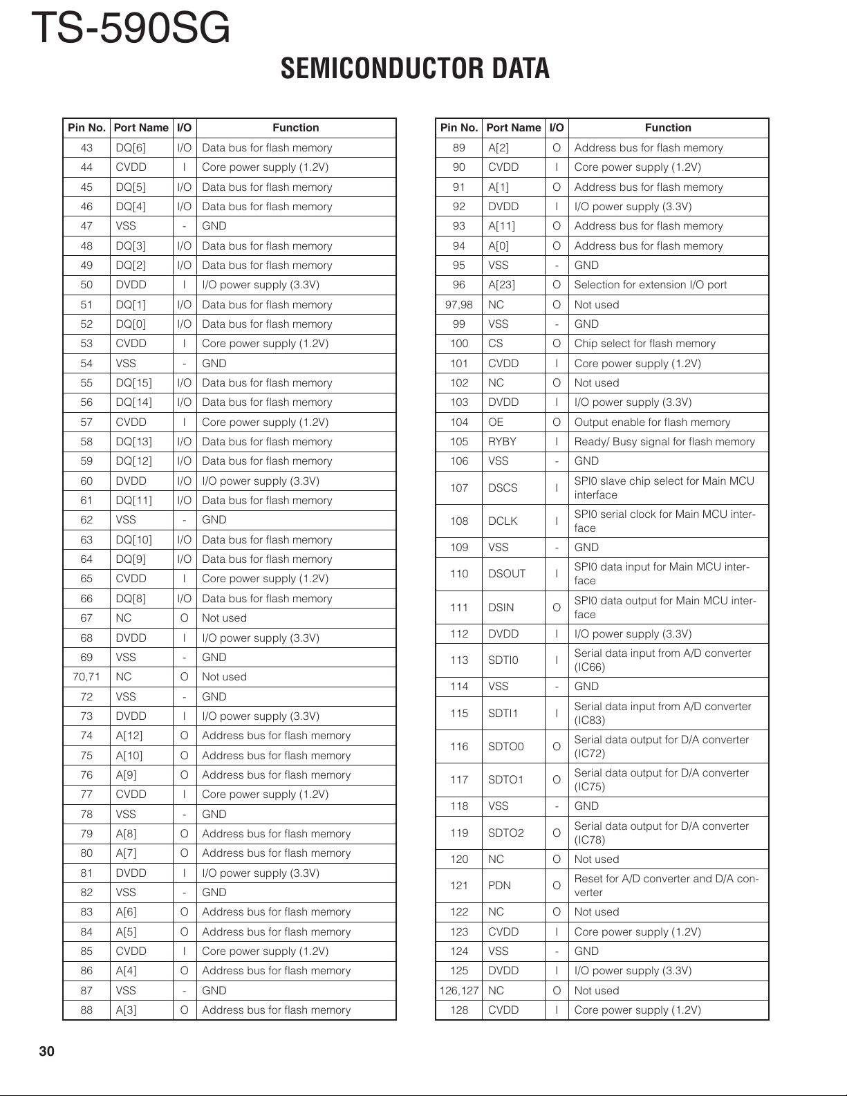
TS-590SG
SEMICONDUCTOR DATA
Pin No. Port Name I/O Function
43 DQ[6] I/O Data bus for fl ash memory
44 CVDD I Core power supply (1.2V)
45 DQ[5] I/O Data bus for fl ash memory
46 DQ[4] I/O Data bus for fl ash memory
47 VSS - GND
48 DQ[3] I/O Data bus for fl ash memory
49 DQ[2] I/O Data bus for fl ash memory
50 DVDD I I/O power supply (3.3V)
51 DQ[1] I/O Data bus for fl ash memory
52 DQ[0] I/O Data bus for fl ash memory
53 CVDD I Core power supply (1.2V)
54 VSS - GND
55 DQ[15] I/O Data bus for fl ash memory
56 DQ[14] I/O Data bus for fl ash memory
57 CVDD I Core power supply (1.2V)
58 DQ[13] I/O Data bus for fl ash memory
59 DQ[12] I/O Data bus for fl ash memory
60 DVDD I/O I/O power supply (3.3V)
61 DQ[11] I/O Data bus for fl ash memory
62 VSS - GND
63 DQ[10] I/O Data bus for fl ash memory
64 DQ[9] I/O Data bus for fl ash memory
65 CVDD I Core power supply (1.2V)
66 DQ[8] I/O Data bus for fl ash memory
67 NC O Not used
68 DVDD I I/O power supply (3.3V)
69 VSS - GND
70,71 NC O Not used
72 VSS - GND
73 DVDD I I/O power supply (3.3V)
74 A[12] O Address bus for fl ash memory
75 A[10] O Address bus for fl ash memory
76 A[9] O Address bus for fl ash memory
77 CVDD I Core power supply (1.2V)
78 VSS - GND
79 A[8] O Address bus for fl ash memory
80 A[7] O Address bus for fl ash memory
81 DVDD I I/O power supply (3.3V)
82 VSS - GND
83 A[6] O Address bus for fl ash memory
84 A[5] O Address bus for fl ash memory
85 CVDD I Core power supply (1.2V)
86 A[4] O Address bus for fl ash memory
87 VSS - GND
88 A[3] O Address bus for fl ash memory
Pin No. Port Name I/O Function
89 A[2] O Address bus for fl ash memory
90 CVDD I Core power supply (1.2V)
91 A[1] O Address bus for fl ash memory
92 DVDD I I/O power supply (3.3V)
93 A[11] O Address bus for fl ash memory
94 A[0] O Address bus for fl ash memory
95 VSS - GND
96 A[23] O Selection for extension I/O port
97,98 NC O Not used
99 VSS - GND
100 CS O Chip select for fl ash memory
101 CVDD I Core power supply (1.2V)
102 NC O Not used
103 DVDD I I/O power supply (3.3V)
104 OE O Output enable for fl ash memory
105 RYBY I Ready/ Busy signal for fl ash memory
106 VSS - GND
107 DSCS I
108 DCLK I
109 VSS - GND
110 DSOUT I
111 DSIN O
112 DVDD I I/O power supply (3.3V)
113 SDTI0 I
114 VSS - GND
115 SDTI1 I
116 SDTO0 O
117 SDTO1 O
118 VSS - GND
119 SDTO2 O
120 NC O Not used
121 PDN O
122 NC O Not used
123 CVDD I Core power supply (1.2V)
124 VSS - GND
125 DVDD I I/O power supply (3.3V)
126,127 NC O Not used
128 CVDD I Core power supply (1.2V)
SPI0 slave chip select for Main MCU
interface
SPI0 serial clock for Main MCU inter-
face
SPI0 data input for Main MCU inter-
face
SPI0 data output for Main MCU inter-
face
Serial data input from A/D converter
(IC66)
Serial data input from A/D converter
(IC83)
Serial data output for D/A converter
(IC72)
Serial data output for D/A converter
(IC75)
Serial data output for D/A converter
(IC78)
Reset for A/D converter and D/A con-
verter
30
 Loading...