

VHF FM TRANSCEIVER / VHF
调频手持对讲机
TK-U100(V
SERVICE MANUAL /
)
维修手册
© 2010-10 PRINTED IN CHINA
B51-8938-00 (N)
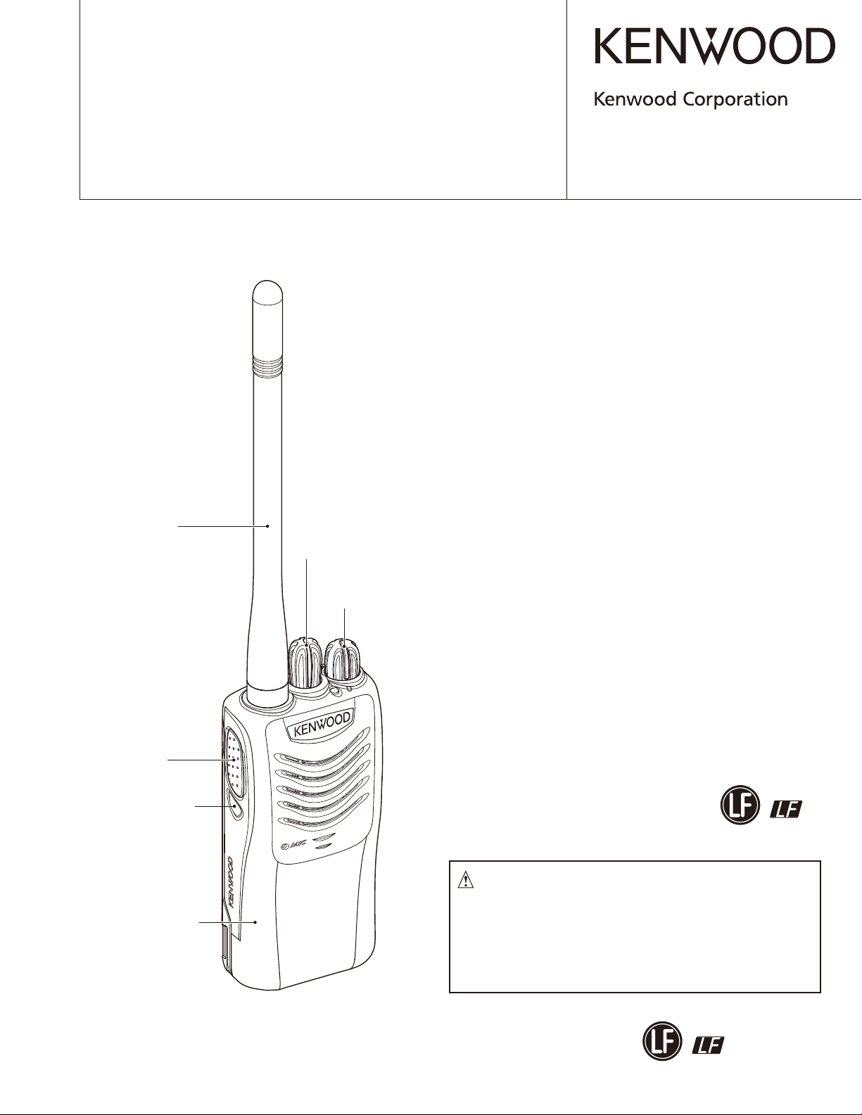
Helical antenna
天线
(KRA-26: Option / 可选件)
(T90-1094-05)
Knob (PTT)
按钮(PTT)
(K29-9489-03)
Button knob (Side)
钮扣按钮(侧面)
(K29-9490-03)
Plastic cabinet assy
机壳
(A02-4135-03)
Knob (Selector)
旋钮(选择器)
(K29-9488-03)
Knob (Volume)
旋钮(音量)
(K29-9487-03)
无铅焊接通信产品
保护环境建伍领先
注意∶本产品是无铅化焊接产品
在维修时请使用无铅焊锡
和相应的焊接工具
详细事项请访问如下网址了解:
This product complies with the
directive for the European market.
RoHS
http://www.kenwoodhk.com.hk/
This product uses Lead Free solder.

TK-U100(V
)
CONTENTS /
GENERAL .....................................................3
SYSTEM SET-UP .........................................4
REALIGNMENT ...........................................5
DISASSEMBLY FOR REPAIR ......................9
CIRCUIT DESCRIPTION ............................11
SEMICONDUCTOR DATA ......................... 16
COMPONENTS DESCRIPTION .................17
PARTS LIST ...............................................19
EXPLODED VIEW ......................................24
ADJUSTMENT ..........................................25
PC BOARD
TX-RX UNIT (X57-8093-00) ...................32
LEVEL DIAGRAM ......................................36
SCHEMATIC DIAGRAM ............................37
目录
概 述 ........................................................................ 3
系统体系 ........................................................................4
模式组合 ........................................................................5
维修拆卸 ........................................................................9
电路说明 ......................................................................11
半导体数据 .................................................................16
元件说明 ......................................................................17
零 件 表 ......................................................................19
部件分解图 .................................................................24
调 整 ......................................................................26
印刷电路板
收发单元 (X57-8093-00) ...............................32
电 平 图 ......................................................................36
原 理 图 ......................................................................37
BLOCK DIAGRAM .....................................41
SPECIFICATIONS ...................BACK COVER
Document Copyrights
Copyright 2010 by Kenwood Corporation. All rights re-
served.
No part of this manual may be reproduced, translated,
distributed, or transmitted in any form or by any means,
electronic, mechanical, photocopying, recording, or otherwise, for any purpose without the prior written permission
of Kenwood.
Disclaimer
While every precaution has been taken in the preparation
of this manual, Kenwood assumes no responsibility for errors or omissions. Neither is any liability assumed for damages resulting from the use of the information contained
herein. Kenwood reserves the right to make changes to any
products herein at any time for improvement purposes.
方 块 图 ......................................................................41
规 格 ................................................................. 封底
文档版权信息
Kenwood Corporation 拥有版权 2010。保留所有权利。
未经 Kenwood公司预先书面同意,无论出于何种目的,均
不得以任何形式或任何方式包括电子、机械、影印、录音或
其他方式复制、翻译、分发或传播本手册的任何部分。
免责声明
Kenwood 公司在准备本文档时已采取所有必要的预防措施,
恕不对错误或疏漏承担任何责任,也不对因使用本文中所含
的信息而导致的损害负责。Kenwood 公司保留出于改进的需要
而随时对文中的产品信息做出更改的权利。
2
TK-U100(V
)
GENERAL /
INTRODUCTION
SCOPE OF THIS MANUAL
This manual is intended for use by experienced technicians familiar with similar types of commercial grade com mu ni ca tions equipment. It contains all required service
in for ma tion for the equipment and is current as of the publication date. Changes which may occur after publication
are covered by either Service Bulletins or Manual Revisions.
These are is sued as required.
ORDERING REPLACEMENT PARTS
When ordering replacement parts or equipment information, the full part identifi cation number should be includ ed.
This applies to all parts : components, kits, or chassis. If the
part number is not known, include the chassis or kit number
of which it is a part, and a suffi cient description of the re quired component for proper identifi cation.
PERSONAL SAFETY
The following precautions are recommended for personal
safety:
• DO NOT transmit until all RF connectors are verifi ed se-
cure and any open connectors are properly terminated.
• SHUT OFF and DO NOT operate this equipment near
elec tri cal blasting caps or in an explosive atmosphere.
• This equipment should be serviced by a qualifi ed techni-
cian only.
概述
引言
本手册的范围
本手册是提供给熟悉通信专业并且具有维修经验的技术人
员使用的。它包括了维修该设备所需要的全部资料和现行出
版日期。在出版后可能发生变动,如果需要,可以参照《维
修通报》或《手册修订本》进行补充。
替换零件的订购
当订购替换零件或设备资料时,应注意完整的零件识别号
码。所有的零件均有识别号码∶元件,组件或机壳。如果不
知道零件的号码,为了正确地识别,必须注明此元件所属的
机壳或组件的号码,并对元件进行充分的说明。
个人安全
为了个人的安全,请注意下列事项∶
• 在没有认真核实所有射频插头之前或有任何一个脱开的插
头没有连接到相应端口上的情况下均不要发射。
• 在电爆管附近或在易燃性气体环境中,必须关闭电源,不
要操作本设备。
• 本设备只应该由有资格的技术人员进行维修。
SERVICE
This transceiver is designed for easy servicing. Refer to
the sche mat ic diagrams, printed circuit board views, and
align ment procedures contained within.
Model Type TX-RX unit
TK-U100(V) C X57-8093-00 144~174MHz
Frequency
range
Remarks
IF1: 38.85MHz
LOC: 38.4MHz
维修服务
为了便于维修本设备,建立了完整的维修服务体系,提供
了包括原理图,印刷电路板图和调整步骤在内的资料供参考。
型 号 类型 收发单元 频率范围 备 注
TK-U100(V) C X57-8093-00 144~174MHz
IF1:38.35MHz
LOC:38.4MHz
3
TK-U100(V
)
SYSTEM SET-UP /
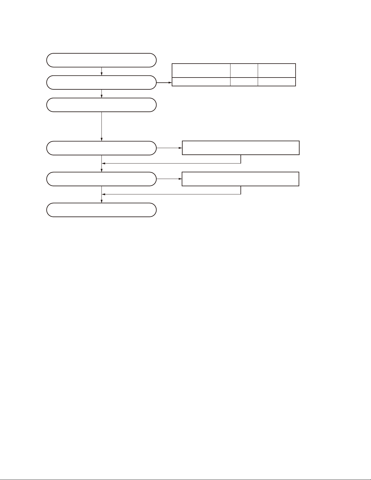
Merchandise received
接收订单
Choose the type of transceiver
选择手持对讲机的类型
Transceiver programming
手持对讲机编程
Are you using the optional antenna?
您使用可选件天线吗?
NO / 否
Are you using the speaker microphone?
您使用扬声器麦克风吗?
NO / 否
Delivery
交货
系统体系
Frequency range (MHz) RF power Type
频率范围 (MHz)
TX/RX 144~174
A personal computer, programming interface (KPG-22/22A),
and FPU (programming software) are required for programming.
(The frequency, TX power HI/LOW, and signaling data are
programmed for the transceiver.)
编程时需要个人计算机,编程接口 (KPG-22/22A)和FPU(编程软件)。
(为手持对讲机设定频率,常规系统特性,TX高/低功率,以及信令数据。)
YES / 是
YES / 是
KRA-22 or KRA-26 Optional antenna
KRA-22或KRA-26
KMC-21 or KMC-45 Speaker microphone
KMC-21或KMC-45
射频功率
5.0W
可选件天线
扬声器麦克风
类型
TK-U100(V) C
(Option)
(可选件)
4
TK-U100(V
)
1. Modes
User mode
PC mode
Clone mode
Mode Function
User mode For normal use.
PC mode
Data programming
mode
PC test mode
Clone mode
PC test mode
Used for communication between the transceiver and PC.
Used to read and write frequency data and
other features to and from the transceiver.
Used to check the transceiver using the PC.
This feature is included in the FPU.
Used to transfer programming data from
one transceiver to another.
REALIGNMENT /
Data programming mode
PC tuning mode
模式组合
1. 模式
用户模式
PC模式
复制模式
模 式 功 能
用户模式 一般使用。
PC 模式 用于手持对讲机与计算机之间的通信。
数据编程模式 用于阅读和写入频率数据以及其他功能。
PC 测试模式
复制模式
PC测试模式
用于使用计算机检测。
此特性包括在 FPU 内。
用于从一个手持对讲机编程数据复制到另
一个手持对讲机。
数据编程模式
PC调谐模式
2. How to Enter Each Mode
Mode Operation
User mode Power ON
PC mode Received commands from PC
Clone mode [PTT]+[Side]+Power ON (Two seconds)
3. PC Mode
3-1. Preface
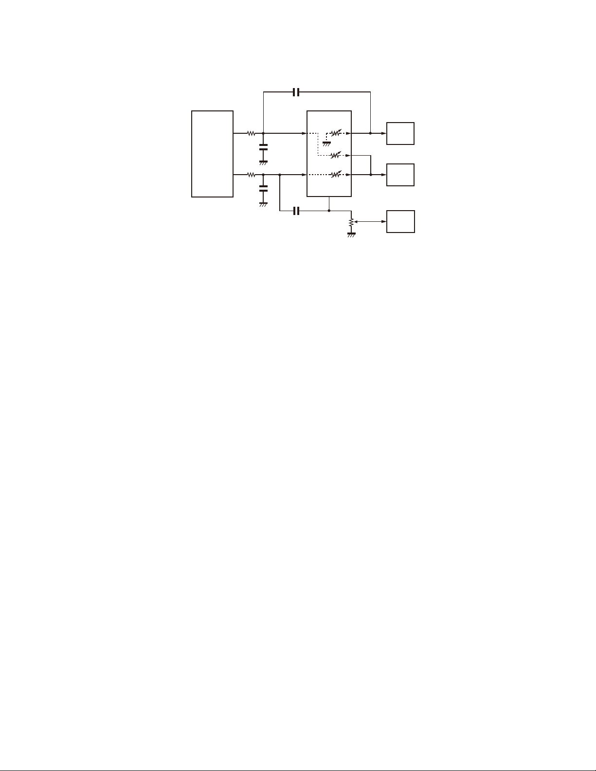
The transceiver is programmed by using a personal computer, a programming interface (KPG-22/22A, USB adapter
(KCT-53U)) and FPU (programming software).
The programming software can be used with a PC. Figure
1 shows the setup of a PC for programming.
3-2. Connection Procedure
1. Connect the transceiver to the personal computer with
the interface cable and USB adapter (when the interface
cable is KPG-22A, the KCT-53U can be used).
Note:
• You must install the KCT-53U driver in the computer to
use the USB adapter (KCT-53U).
• When using the USB adapter (KCT-53U) for the fi rst time,
plug the KCT-53U into a USB port on the computer with
the computer power ON.
2. 如何进入每一种模式
模 式 操 作
用户模式 接通电源
PC 模式 PC 模式
复制模式 [PTT]+[ 侧面 ]+ 接通电源 (2 秒钟 )
3. PC 模式
3-1. 前言
手持对讲机采用个人电脑、编程接口 (KPG-22/22A,USB 适
配器 (KCT-53U)) 和 FPU( 编程软件 ) 进行编程。
编程软件可以在 P C 上进行使用。图 1 给出了 PC 进行编程
的设置。
3-2. 连接操作
1. 使用接口电缆和 U S B 适配器将手持对讲机连接到个人电脑
( 接口电缆为 KPG-22A 时,可以使用 KCT-53U)。
注意 :
• 必须在电脑上安装 K C T -53U 驱动程序才能使用 U S B 适配器
(KCT-53U)。
• 首次使用 US B 适配器 (KCT-53U ) 时,请在电脑开机的情况
下将 KCT-53U 插入电脑的 USB 端口。
5
TK-U100(V
)
REALIGNMENT /
2. When the POWER is switched on, user mode can be entered immediately. When the PC sends a command, the
transceiver enters PC mode.
When data is read from the transceiver, the red LED
lights.
When data is written to by the transceiver, the green LED
lights.
Note:
• The data stored in the personal computer must match
Model Name and Model Type when it is written into EEPROM.
• Do not press the [PTT] key during data transmission or
reception.
3-3. KPG-22/KPG-22A Description
(PC programming interface cable: Option)
The KPG-22/22A is required to interface the transceiver
with the computer. It has a circuit in its D-sub connector
(KPG-22: 25-pin, KPG-22A: 9-pin) case that converts the RS232C logic level to the TTL level.
The KPG-22/22A connects the SP/MIC connector of the
transceiver to the RS-232C serial port of the computer.
模式组合
2. 手持对讲机电源打开时,可以立即进入用户模式。P C 发送
指令时,手持对讲机进入 PC 模式。
手持对讲机发送数据时,红色的 LED 点亮。
手持对讲机接收数据时,绿色的 LED 点亮。
注意 :
• 个人电脑保存的数据写入 EEPROM 时,必须与机型和类型相
符。
• 请勿在数据发送或接收期间按 [PTT] 键。
3-3. KPG-22/KPG-22A 说明
(PC 编程接口电缆 :选购件 )
将手持对讲机与电脑相连需要 KPG-22/22A。该电缆的
D-sub 连接器 (KPG-22 :25 针,KPG-22A :9 针 ) 盒具有将 RS232C 逻辑电平转换为 TTL 电平的电路。
KP G -22/22A 将手持对讲机的 SP/MIC 连接器连接到电脑的
RS-232C 串行端口。
3-4. KCT-53U Description (USB adapter: Option)
The KCT-53U is a cable which connects the KPG-22A to a
USB port on a computer.
When using the KCT-53U, install the supplied CD-ROM
(with driver software) in the computer. The KCT-53U driver
runs under Windows 2000, XP or Vista (32-bit).
3-5. FPU (Programming Software) Description
The FPU is the programming software for the transceiver
supplied on a CD-ROM. This software runs under windows
XP, Vista or 7 on a PC. The software on this disk allows a
user to program the transceiver via Programming interface
cable (KPG-22/22A).
Note:
Use the FPU that matches the market when you fi rst set
the market code and model name/frequency data to the
service unit. The unit set by mistake cannot be restored.
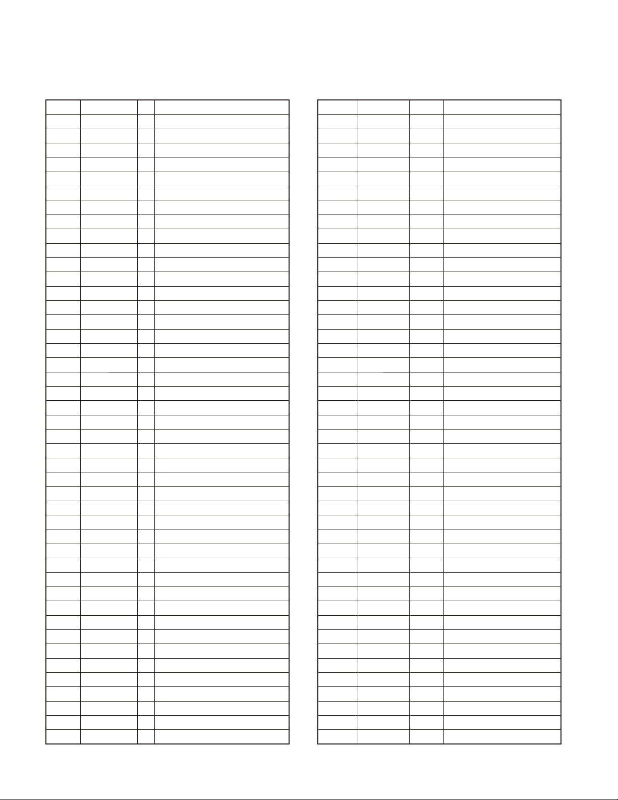
Receive frequencies listed below may result in the interference of reception due to the harmonics of internal oscillators.
Enter a frequency not listed in the table.
No. Frequency (MHz) No. Frequency (MHz)
1 152.69375 9 153.60500
2 152.69500 10 153.60625
3 152.70000 11 172.79375
4 152.70500 12 172.79500
5 152.70625 13 172.80000
6 153.59375 14 172.80500
7 153.59500 15 172.80625
8 153.60000
3-4. KCT-53U 说明 (USB 适配器 :选购件 )
KCT-53U 是将 KPG-22A 连接到电脑 USB 端口的电缆。
使用 K C T -53U 时,请在电脑上安装附带的 CD-ROM( 带有
驱动程序软件 )。KC T -53U 驱动程序在 Windows 2000, X P 或
Vista(32 位 ) 下运行。
3-5. FPU( 编程软件 ) 说明
FPU 是 CD-ROM 附带的用于手持对讲机的编程软件。该软件
在 PC 的 Windows XP、Vista 或 7 下运行。该光盘上的软件允
许用户通过编程接口电缆 (KPG-22/22A) 对手持对讲机进行编
程。
注意 :
初次设置服务单元的市场代码和机型 / 频率数据时,请使
用与市场相符的 FPU。若单元设置有误,将无法予以恢复。
下面列出的接收频率由于内部振荡器的谐波可能对信号接
收造成干扰。
输入在表格中没有列出的频率
编号
1 152.69375 9 153.60500
2 152.69500 10 153.60625
3 152.70000 11 172.79375
4 152.70500 12 172.79500
5 152.70625 13 172.80000
6 153.59375 14 172.80500
7 153.59500 15 172.80625
8 153.60000
(MHz) 编号
频率
频率
(MHz)
6
TK-U100(V
)
REALIGNMENT /
3-6. Programming with PC
If data is transferred to the transceiver from a PC with the
FPU, the data for each set can be modifi ed.
Data can be programmed into the EEPROM in RS-232C
format via the SP/MIC jack.
In this mode the PTT line operate as TXD and RXD data
lines respectively.
List of FPU for transceiver
Model Type FPU
TK-U100(V) C KPG-137D(C)
KPG-22 or KPG-22A or KPG-22A + KCT-53U
KPG-22或KPG-22A或KPG-22A + KCT-53U
PC
FPU
Illustration is KPG-22
插图为KPG-22
模式组合
3-6. 使用 PC 编程
如果使用 FPU 将数据从 PC 传输到手持对讲机,则每套手持
对讲机的数据均可修改。
通过 SP/MIC 插孔可以将数据以 RS-232C 格式写入 EEPROM。
在该模式下,PTT 线路分别用作 TXD 和 RXD 数据线路。
手持对讲机的 FPU 名单
型 号 类 型
TK-U100(V) C KPG-137D(C)
PC
D-SUB
(25-pin/25针)
KPG-22
Transceiver
手持对讲机
PC
D-SUB
(9-pin/9针)
KPG-22A
Transceiver
手持对讲机
Transceiver
手持对讲机
FPU
PC
USB
KCT-53U
KPG-22A
Gray
Gray/Black
1.5D-XV Lead wire
1.5D-XV Shield wire
Tuning cable / 调谐电缆
(E30-3216-05)
灰色
灰色/黑色
1.5D-XV导线
1.5D-XV屏蔽线
Fig. 1 /
图1
+
SP
–
+
MIC
–
7
TK-U100(V
)
REALIGNMENT /
4. Clone Mode
Programming data can be transferred from one transceiver to another by connecting them via their SP/MIC connectors.
Cloning can be performed as described below (the transmit transceiver is the source and the receive transceiver is
the target).
The following data cannot be cloned.
• Tuning data
• Model name data
• ESN data
1. Turn the source transceiver and target transceiver power
OFF.
2. Turn the source transceiver power ON while pressing the
[PTT] and [Side] keys, to enter clone mode.
3. Connect the cloning cable (part No. E30-3410-05) to the
SP/MIC connectors on the source and target transceivers.
4. Turn the target transceiver power ON.
5. Press the [Side] key on the source transceiver.
The data of the source is sent to the target. While the
source is sending data, red LED will light. While the target
is receiving the data, green LED will light. When cloning
of data is completed, the source red LED turned off, and
the target automatically operates in the User mode.
6. Additional targets can be continuously cloned. When the
[Side] key on the source is pressed, the data of source is
sent to the target again. Repeat steps 3 to 5 to clone ad-
ditional transceivers.
Note:
• The Model name and Market codes must be the same in
order to clone the transceiver.
• If the transceivers clone mode is confi gured as “Disabled”,
the transceiver cannot enter clone mode.
• If the Read authorization password is set to the transceiv-
er, the transciever cannot enter to the clone mode.
• Cannot be cloned if the password (overwrite password) is
programmed to the target.
模式组合
4. 复制模式
用 SP/MIC 连接器连接手持对讲机,可以将编程数据从一台
手持对讲机传输到另一台手持对讲机。
如下所述可进行复制(发射手持对讲机为主机,接收手持
对讲机为子机)。
以下数据不能复制。
·调谐数据
·机型数据
·ESN 数据
1. 关闭主机和子机的电源。
2. 按 [PTT]和[侧面]键的同时打开主机的电源,使其进入
复制模式。
3. 将复制电缆(零件号 E30-3410-05)连接到主、子机的 S P /
MIC 连接器上。
4. 打开子机的电源。
5. 按主机上的 [ 侧面 ] 键。
主机的数据便被发送到子机。主机发送数据时,红色 L E D
将呈。子机接收数据时,绿色 LED 呈。数据复制完成后,
主机的红色 LED 熄灭,子机自动以用户模式运行。
6. 可以继续复制其他子机。按主机上的 [ 侧面 ] 键,主机的
数据再次被发送到子机。重复步骤3~5复制其他手持对
讲机。
注意 :
· 机型和市场代码必须相同才能复制手持对讲机。
• 如果手持对讲机复制模式被设置为“无效”,则手持对讲机
不能进入复制模式。
• 如果手持对讲机设置了读取授权密码,则手持对讲机无法
进入复制模式。
• 如果子机编程设有密码 ( 改写密码),则无法复制。
Cloning cable
复制电缆
(E30-3410-05)
8
TK-U100(V
)
DISASSEMBLY FOR REPAIR /
1. Separating the Case Assembly from the
Chassis
1. Remove the two knobs (q).
2. Remove the two screws (w).
3. Expand the right and left sides of the bottom of the case
assembly, lift the chassis, and remove it from the case
assembly (e).
4. Taking care not to cut the speaker lead (r), open the
chassis and case assembly.
Note: Solder the speaker wire back in its original position if
you have removed it.
@
@
.
维修拆卸
1. 从机架上分离外壳
1. 取下两旋扭 (q)。
2. 取下两颗螺钉 (w)。
3. 掀开外壳底部的左右两侧,取下机架,并外壳中取出 (e)。
4. 小心不要折断扬声器引线 (r)。拆下机架和外壳。
注意 :
如果取下了扬声器的导线,请将其焊接到原位上。
:
:
;
GRN /
BRN /
绿色
褐色
9
TK-U100(V
)
DISASSEMBLY FOR REPAIR /
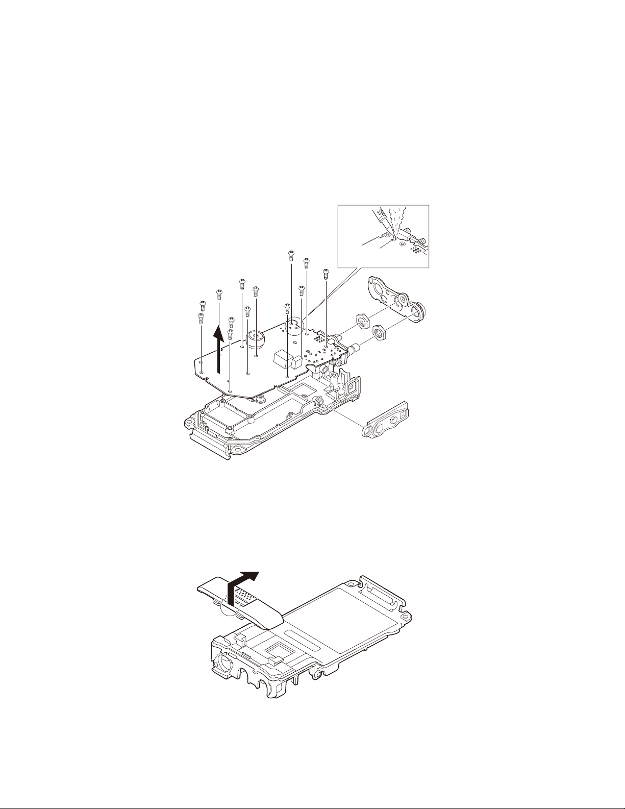
2. Removing the TX-RX unit from the
Chassis
1. Remove the packing (t).
2. Remove the 13 screws (y).
3. Remove the packing (u) and two hexagon nuts (i).
4. Remove the solder from the antenna terminal using a sol-
dering iron then lift the unit off (o).
Note: When reassembling the unit in the chassis, be sure
to solder the antenna terminal.
B
维修拆卸
2. 拆卸收发单元
1. 取下橡胶垫 (t)。
2. 取下 13 颗螺钉 (y)。
3. 取下橡胶垫 (u) 和两个六角形螺母 (i)。
4. 用电烙铁烫开天线端点处的焊锡 , 并拆卸主板 (o)。
注意 :
当重新将主板安装到机架上时,确保将天线端点处焊接
好。
8
Antenna terminal
天线端点
>
2
2
3. Removing the Rear Panel
1. Raise the rear panel on the chassis (!0).
=
3. 取下后面板
1. 从机架上提起后面板 (!0)。
10
TK-U100(V
)
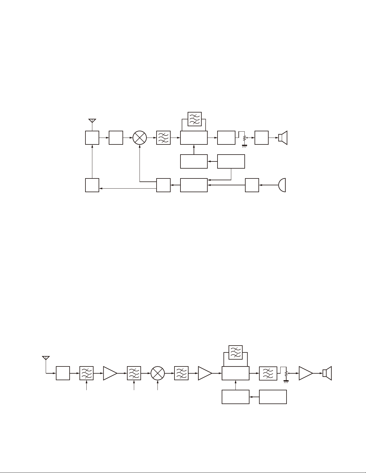
CIRCUIT DESCRIPTION /
1. Frequency Confi guration
The receiver utilizes double conversion. The first IF is
38.85MHz and the second IF is 450kHz. The fi rst Local oscillator is supplied from the PLL circuit.
The PLL circuit in the transmitter generates the neces-
sary frequencies.
TX/RX: 144~174MHz
ANT
1st MIX MCF SP
ANT
SW
TX
AMP
RF
AMP
144~174MHz
38.85MHz
182.85~
212.85MHz
RF
AMP
电路说明
1. 频率构成
接收部采用二次变频超外差方式。第一中频为 38.85M H z,
第二中频为 450kHz。第一本振频率信号由锁相环电路提供。
发射部由锁相环电路直接产生所需的频率。
CF
450kHz
IF
SYSTEM
38.4MHz
X2
doubler
PLL
VCO
AF
filter
TCXO 19.2MHz
AF
AMP
MIC
MIC
AMP
Fig. 1 Frequency confi guration /
2. Receiver System
The receiver system is shown in Figure 2.
2-1. Front End (RF Amplifi er) Circuit
The signal coming from the antenna passes through the
transmit/receive switching diode circuit (D101, D102, and
D103) and a BPF (L210), and is then amplifi ed by the RF amplifi er (Q204).
The resulting signal passes through a BPF (L207 and
L208) and goes to the mixer. These BPFs are adjusted by
variable capacitors (D201 and D202). The input voltage to
the variable capacitor is a regulated voltage output from the
DAC (IC300).
ANT
BPF
ANT
SW
Q204
RF AMP XF200
BPF
Q203
1st MIX
MCF
图 1 频率构成
2. 接收部系统
接收部系统的如图 2 所示。
2-1. 前端 ( 高频放大器 ) 电路
从天线接收的信号进入发送 / 接收转换开关二极管电路
(D101、D102 和 D103),然后通过 BPF(L210),并且被射频放
大器 (Q204) 放大。
此信号通过 BPF(L207 和 L208) 然后进入混频。这些 BPF 被
可变电容器 ( D201 和 D202) 调整。输入可变电容器的电压被
经 DAC(IC300) 的电压输出调整。
CF200
Q202
IF AMP
IC200
IF,MIX,DET
IC303
AF filter
VR500
IC302
AF PA
SP
BPF
BPF 1st Local
Fig. 2 Receiver system /
Q201
X2 doubler
2nd Local
图 2 接收部系统
X1
TCXO
19.2MHz
11

TK-U100(V
)
CIRCUIT DESCRIPTION /
2-2. First Mixer
The signal from the front end is mixed with the fi rst local
oscillator signal generated in the PLL circuit by Q203 to produce a fi rst IF frequency of 38.85MHz.
The resulting signal passes through the XF200 MCF to
cut the adjacent spurious and provide the optimum characteristics, such as adjacent frequency selectivity.
2-3. IF Amplifi er Circuit
The fi rst IF signal is passed through a four-pole monolithic
crystal fi lter (XF200) to remove the adjacent channel signal.
The fi ltered fi rst IF signal is amplifi ed by the fi rst IF amplifi er (Q202) and then applied to the lF system IC (IC200).
The IF system IC provides a second mixer, second local
oscillator, limiting amplifier, quadrature detector and RSSI
(Received Signal Strength Indicator). The second mixer
mixes the fi rst IF signal with the 38.4MHz of the second local oscillator output (TCXO X1) and produces the second IF
signal of 450kHz.
The second IF signal is passed through the ceramic fi lter
(CF200) to remove the adjacent channel signal. The fi ltered
second IF signal is amplified by the limiting amplifier and
demodulated by the quadrature detector with the ceramic
discriminator (CD200). The demodulated signal is routed to
the audio circuit.
电路说明
2-2. 第一混频器
前端的信号与 P LL 电路产生的第一本振信号在 Q203 混频,
生成 38.85MHz 频率的第一中频信号。
生成的信号通过 XF200 MCF。
2-3. 中频放大电路
第一中频信号通过晶体滤波器 ( X F200) 消除相邻信道的信
号。经滤波的第一中频信号被第一中频放大器 (Q202) 放大并
进入中频系统芯片 (IC200)。
中频系统芯片提供第二混频器、第二本振信号、限幅放大器、
正交检测器和 RSSI( 接收信号强度指示器 )。第二混频器将第
一中频信号与 38.4MHz 的第二本振信号输出 (TCXO X1) 进行
混频,并生成 450kHz 的第二中频信号。
第二中频信号通过陶瓷滤波器 ( C F200) 继续消除相邻信道
的信号。经滤波的第二中频信号被限幅放大器放大并被带有
陶瓷鉴频器 ( C D200) 的正交检测器解调。经解调的信号进入
音频电路。
2-4. Audio Amplifi er Circuit
The demodulated signal from IC200 is amplifi ed by IC305,
IC303 and goes to AF amplifi er through IC302.
The signal then goes through an volume control (VR500),
and is routed to an audio power amplifi er (IC302) where it is
amplifi ed and output to the speaker.
To output sounds from the speaker, IC400 sends a high
signal to the SPMUT line and turns IC400 on through Q300,
Q301, Q302 and Q306.
3. Transmitter System
3-1. Microphone Amplifi er Circuit
The signal from microphone amplifi ed by IC301 and goes
through mute switch (IC300).
IC304 is composed of high-pass fi lter, low-pass fi lter and
pre-emphasis/IDC circuit.
The output signal from the DAC IC (IC300) goes to the
VCO modulation input.
MIC
IC301
BUFF
MIC
AMP
IC304
2-4. 音频放大器电路
来自于 I C200 的解调信号被 IC305 放大,并 通 过 I C302,
IC303 送到 AF 放大器。
信号通过 AF 音量控制 (VR500),在音频功率放大器 (IC302)
进行放大后输出到扬声器。
由扬声器输出声音时,IC400 发送高电平信号给 SPMUT,通
过 Q300、Q301、Q302 和 Q306 打开 IC400。
3. 发射机系统
3-1. 麦克风放大器电路
麦克风的信号被 IC301 放大,然后通过静音开关 (IC300)。
IC304 由高通滤波器、低通滤波器和预加重 /IDC 电路组成。
DAC IC(IC300) 的输出信号送入 VCO 调制输入。
IC300
VCO
DAC
LSDO LSDO
X1
TCXO
12
Fig. 3 Microphone amplifi er circuit /
图 3 麦克风放大器电路
TK-U100(V
)
CIRCUIT DESCRIPTION /
3-2. Driver and Final Amplifi er Circuit
The signal from the T/R switch (D100 is on) is amplifi ed
by the pre-drive amplifi er (Q100) to 30mW.
The output of the pre-drive amplifi er is amplifi ed by the
drive amplifi er (Q101) and the RF fi nal amplifi er (Q102) to
5.0W (1W when the power is low).
The drive amplifi er and the RF fi nal amplifi er consist of
two MOS FET stages.
The output of the RF final amplifier is then passed
through the harmonic fi lter (LPF) and antenna switch (D101
and D102) and is applied to the antenna terminal.
From
T/R SW
(D100)
+B
Q100
Pre-DRIVE
AMP
R121
R122
R123
Q101
DRIVE
AMP
VDD
电路说明
3-2. 驱动器和末级放大器电路
来自于 T/R 开关 (D100 ON) 的信号被预驱动放大器 (Q100)
放大到 30mW。
预驱动放大器的输出被驱动放大器 ( Q101) 和射频末级放大
器 (Q102) 放大到 5.0W( 当低功率时为 1W)。
驱动放大器和 RF 末级放大器由 2 个 MOS FET 构成。
射频末级放大器的输出通过谐波滤波器 (LPF)和天线开关
(D101 和 D102) 并且送到天线终端。
ANT
VG
D101,102
ANT
SW
LPF
Q102
RF FINAL
AMP
POWC
CURDET
Fig. 4 Drive and fi nal amplifi er circuit /
4. Frequency Synthesizer Circuit
4-1. Frequency Synthesizer
The frequency synthesizer consists of the TCXO (X1),
VCO, PLL IC (IC1) and buffer amplifi ers.
The TCXO generates 19.2MHz. The frequency stability is
5.0ppm within the temperature range of –30 to +60°C.
The frequency tuning and modulation of the TCXO are
done to apply a voltage to pin 1 of the TCXO. The output of
the TCXO is applied to pin 1 of the PLL IC.
The VCO consists of 1VCO and covers a dual range of the
144.00~174.00MHz and the 182.85~212.85MHz. The VCO
generates 182.85~212.85MHz for providing to the fi rst local
signal in receive.
The PLL IC consists of a prescaler, reference divider,
phase comparator, charge pump (The frequency step of the
PLL circuit is 5 or 6.25kHz).
PLL data is output from DATA (pin 19), CLOCK (pin 18)
and PLDL (pin 20) of the MCU (IC400). The data are input to
the PLL IC when the channel is changed or when transmission is changed to reception and vice versa. A PLL lock condition is always monitored by the pin 22 (PLUL) of the MCU.
When the PLL is unlocked, the PLUL goes low.
图 4 驱动及末级放大器电路
4. 频率合成器电路
4-1. 频率合成器
频率合成器由 TCXO(X1)、VCO、PLL IC(IC1) 和缓冲放大器
组成。
TCXO 产生 19.2MHz 的频率。在温度为 -30 ~ +60℃的范围内,
频率的稳定性为 5.0ppm。进行频率调谐和 TCXO 调制,以便给
TCXO 的针脚 1 提供电压。TCXO 的输出加在 PLL IC 的针脚 1 上。
VCO由 1VCO组成,并且覆盖了 144.00 ~ 174.00MH z 和
182.85 ~ 212.85MHz 双波段。VCO 产生 182.85 ~ 212.85MHz
的频率,以提供接收的第一个本振信号。
P L L I C 由预计数器、基准除法器、相位比较器、电荷泵组
成 (PLL 电路的频率步长为 5kHz 或 6.25kHz)。
PLL 数据从 MCU(IC400) 的 DATA( 针脚 19),CLOCK( 针脚
18) 和 PLDL( 针脚 20) 输出。当信道改变时,或当由发射
变为接收或由接收变为发射时,数据输入 P L L I C。P L L 的
锁定条件总是由 MCU 的针脚 22(PLUL) 监控。当 PLL 失锁时,
PLUL 为低电位。
13
TK-U100(V
)
CIRCUIT DESCRIPTION /
Q5
T/RSHF
(TX: Low)
VCO
PLUL
IC400
MCU
Fig. 5 PLL block diagram /
5. Control Circuit
The control consists of the MCU (IC400) and its peripheral circuits. It controls the TX-RX unit. IC400 mainly performs
the following;
1) Switching between transmission and reception by PTT
signal input.
2) Reading channel information, frequency, and program
data from the memory circuit.
3) Sending frequency program data to the PLL.
4) Controlling squelch on/off via the DC voltage from the
squelch circuit.
5) Controlling the audio mute circuit via the decode data in-
put.
6) Transmitting tone and encode data.
BUFF
CV
Q1
INV
DATA,CLOCK,PLDL
5
14
电路说明
D200
SWLPF
X1
TCXO
D100
SW To
RF AMP
To mixer
LSDO
Q6
RF
AMP
8
IC1
PLL
1
图 5 PLL 方块图
5. 控制电路
控制电路是由微处理器 ( IC400) 和外部电路构成。它控制
收发单元。IC400 的主要功能如下 :
1) 根据 PTT 的输入信号来转换发射和接收状态。
2) 从存储电路读出信道信息、频率以及编程数据。
3) 发送频率数据给 PLL。
4) 根据静噪电路输出的 DC 电压来控制静噪的开启和关闭。
5) 根据解码数据控制音频静音。
6) 发射 Tone 及编码数据。
注意 :
EEPROM 保存调谐数据 ( 频偏、静噪等 )。
更换 EEPROM 后,请重新校正手持对讲机。
Note:
The EEPROM stores tuning data (Deviation, Squelch, etc.).
Realign the transceiver after replacing the EEPROM.
6. Signaling Circuit
6-1. Encode
Low-speed data (QT, DQT)
■
Low-speed data is output from pin 49 (LSDO) of the MCU
(IC400). The signal passes through a low-pass CR fi lter. The
signal is mixed with the audio signal and goes to the VCO
and TCXO (X1) modulation input after signal processing in
the DAC IC (IC300).
High-speed data (DTMF)
■
High-speed data (HSD) is output from pin 50 (HSDO) of
the MCU.
The signal passes through a low-pass CR fi lter. TX deviation making an adjustment by MCU is applied to the DAC IC
(IC300). The signal is mixed with the audio signal and goes
to the VCO and TCXO.
14
6. 信令电路
6-1. 编码
■低速数据 (QT, DQT)
低速数据从微处理器 ( IC400) 的针脚 49(LSDO) 输出。信
号通过低通 CR 滤波器。此信号与音频信号混合,在 DAC
IC(IC300) 中进行信号处理之后,进入 VCO 和 TCXO(X1) 调制
输入。
■高速数据 (DTMF)
高速数据 (HSD) 从微处理器的针脚 50(HSDO) 输出。
信号通过低通 C R 滤波器。由微处理器进行调整的 T X 频偏
被施加到 DAC IC(IC300)。此信号与音频信号混合,然后送入
VCO 和 TCXO。
TK-U100(V
)
CIRCUIT DESCRIPTION /
IC400
MCU
49
LSDO
50
HSDO
Fig. 6 Encode /
6-2. Decode
QT/DQT
■
The output signal from IF IC (IC200) enters the MCU
(IC400) through IC300. IC400 determines whether the QT
or DQT matches the preset value, and controls the SPMUT
and the speaker output sounds according to the squelch results.
电路说明
IC300
DAC
21
18
12
图6 编码
6-2. 解码
■ QT/DQT
( I C400)。I C400 确认 Q T 或 D Q T 是否与预设值匹配,控制
SPMUT,然后扬声器根据静噪结果输出声音。
24
FADJ
20
19
MOD
BEEP
IF IC(IC200) 的输出信号通过 IC300 送入微处理器
TCXO
VCO
AF
AMP
7. Power Supply
There are fi ve 5V power supplies for the MCU:
5M is always output while the power is on.
5C is a common 5V and is output when SAVE is not set
to ON.
5R is 5V for reception and output during reception.
5T is 5V for transmission and output during transmission.
5MS is 5V for the SP/MIC connector and the DAC IC
(IC300).
7. 电源
微处理器有5个5V电源。
电源打开时,5M 总是输出。
5C 是普通的 5V 电源,它在 SAVE 没有设为 ON 时输出。
5R 是接收用 5V 电源,它在接收期间输出。
5T 是为发射用的 5V 电源,它在发射期间保持输出。
5MS 是 SP/MIC 和 DAC IC(IC300) 的 5V 电源。
15
TK-U100(V
)
SEMICONDUCTOR DATA /
MCU: F2136ACNKDRB (TX-RX unit IC400)
Pin No. Signal Name I/O Function
1NC ONC
2 VREF - Reference voltage input
3 MODE I Mode select for MCU
4,5 NC O NC
6 RESET I Reset signal input
7 XOUT O Oscillation circuit
8 Vss - GND
9 XIN I Oscillation circuit
10 Vcc - Power supply
11 BSFT O Beat shift for MCU clock
12~14 NC O NC
15 E2WP O Write protect for EEPROM
16 E2DAT I/O Data input/output from EEPROM
17 E2CLK O Clock for EEPROM
18 CLOCK O Clock for PLL/DAC IC
19 DATA O Data for PLL/DAC IC
20 PLDL O Load enable for PLL IC
21 PLPS O Power saving for PLL IC
22 PLUL I Lock detect signal from PLL IC
23 NC O NC
24 EN4 I Encoder input 4
25 EN3 I Encoder input 3
26 EN2 I Encoder input 2
27 EN1 I Encoder input 1
28 NC O NC
29 OPTDET I 2pin option detection
30 LEDR O LED (Red) control
31 LEDG O LED (Green) control
32 SPMUT O Power switch for AF amp
33 NC O NC
34 5TC O 5T control
35 5CC O 5C control
36 5MSC O 5MS control
37 DACLD O Load enable for DAC IC
38 PTT I PTT key input
39 PFKEY I Side key input
40 INT I INT signal input
41 VDCSW O Voltage discharge switch
42 WID/NAR O Wide/Narrow control
43 RXD I Serial data input (FPU)
44 TXD O Serial data output (FPU)
45,46 NC O NC
47 VOXIN I VOX level input
48 CVDET I VCO voltage detection
半导体数据
MCU: F2136ACNKDRB( 收发单元 IC400)
管脚号 接口名称
1 NC 输出 未连接
2 VREF - 基准电压
3 MODE 输入 选择模式 (MCU)
4,5 NC 输出 未连接
6 RESET 输入 MCU 复位
7 XOUT 输出 MCU 时钟输出
8 Vss - 接地
9 XIN 输入 11.0592MHz 时钟输入
10 Vcc - 5.0V
11 BSFT 输出 拍频偏移
12~14 NC 输出 未连接
15 E2WP 输出 EEPROM 写入控制
16 E2DAT
17 E2CLK 输出 EEPROM 时钟
18 CLOCK 输出 PLL/DAC 时钟
19 DATA 输出 PLL/DAC 数据
20 PLDL 输出 PLL 启用
21 PLPS 输出 PLL 省电状态控制
22 PLUL 输入 PLL 失锁检测
23 NC 输出 未连接
24 EN4 输入 编码器输入 4
25 EN3 输入 编码器输入 3
26 EN2 输入 编码器输入 2
27 EN1 输入 编码器输入 1
28 NC 输出 未连接
29 OPTDET 输入 耳机检测
30 LED_R 输出 红色 LED 控制
31 LED_G 输出 绿色 LED 控制
32 SPMUT 输出 AF IC 开关
33 NC 输出 未连接
34 5TC 输出 5T 控制
35 5CC 输出 5C 控制
36 5MSC 输出 5MS 控制
37 EVOLLD 输出 DAC 启用
38 PTT 输入 PTT 键输入
39 PFKEY 输入 侧面键输入
40 INT 输入 MCU 停止
41 VDCSW 输出 电压放电开关
42 WID/NAR 输出 宽 / 窄切换
43 RXD 输入 串行数据输出 (FPU)
44 TXD 输出 串行数据输入 (FPU)
45,46 NC 输出 未连接
47 VOXIN 输入 VOX 水平输入
48 CVDET 输入 VCO 电压电平
输入/输出
输入/输出
功 能
EEPROM 数据输入 / 输出
16
 Loading...