Kenwood Z-828, KD-CZ-828 Service Manual

©
2001-5 PRINTED IN JAPAN
B51-7790-00 (N) 1737
CD●MD-CH CONTROL MP3 CD RECEIVER
KDC-Z828
Z828
SERVICE MANUAL
SIZE AAA BATTERY
(Not supplied)
SRC
PWR
OFF
47Wx4
S.A
FM
AM
DISC
CD MD-CH CONTROL MP3 CD RECEIVER
EX
KDC-Z828
AUD
4.5V
PREOUT
LOUD
DISP
SCAN RDM REP M.RDM AUTO
AME
MENU
NAME.S
NF
COMPACT
DIGITAL AUDIO
2
ZONE
DAB
TEXT
SRC
PWR
OFF
47Wx4
S.A
FM
AM
DISC
CD MD-CH CONTROL MP3 CD RECEIVER
EX
Z828
AUD
4.5V
PREOUT
LOUD
DISP
SCAN RDM REP M.RDM AUTO
AME
MENU
NAME.S
NF
COMPACT
DIGITAL AUDIO
2
ZONE
DAB
TEXT
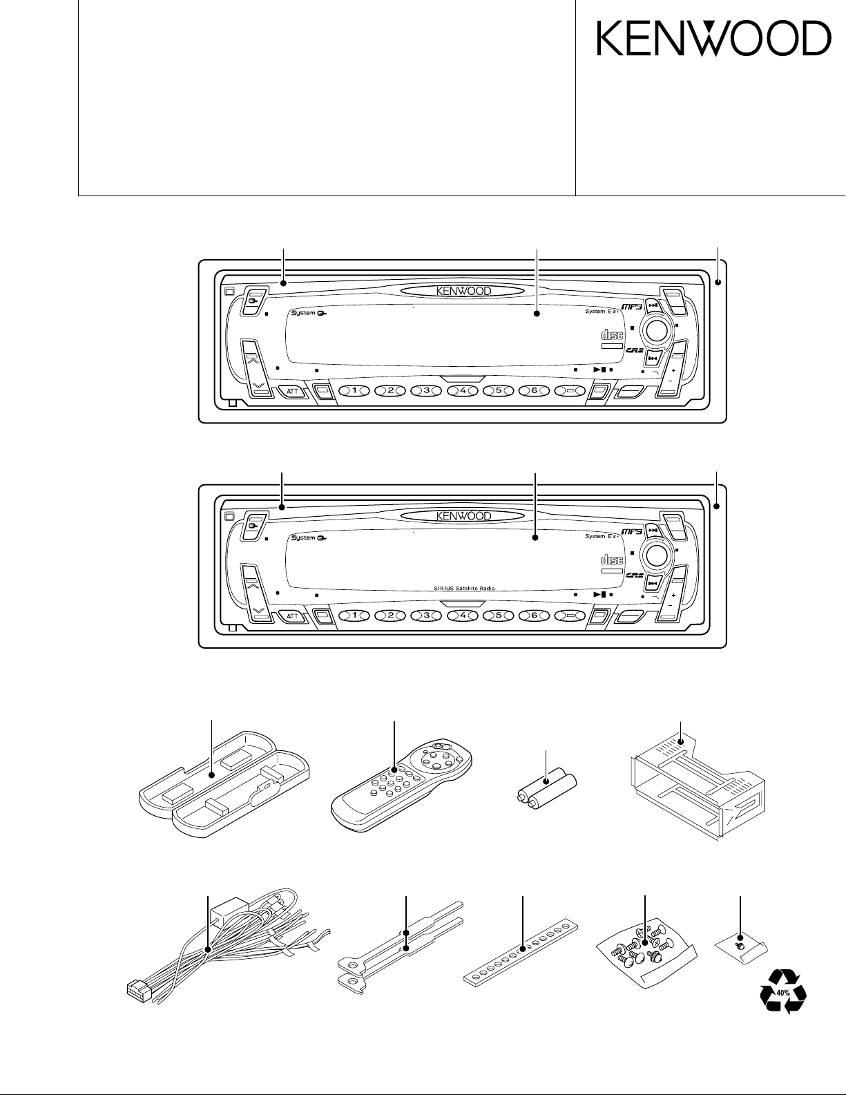
Plastic cabinet assy
(A02-2711-08)
Panel assy
(A64-2473-08)
Front glass assy
(B10-4201-08)
Escutcheon
(B07-3038-08)
Panel assy
(A64-2625-08)
Front glass assy
(B10-4200-08)
Escutcheon
(B07-3048-08)
Remote controller assy
(A70-0894-05)
Mounting hardware assy
(J21-9585-18)
DC cord assy
(E30-6021-08)
Lever
(D10-4364-08)x2
Stay
(J54-0606-04)
Screw set
(N99-1700-05)
Screw set
(N99-1716-08)
KDC-Z828
Z828
RC-520

2
AM
FM
220mV
490mV
FM : 400Hz 75kHzDEV 60dBuV
AM : 400Hz 30%MOD 74dBuV
: 1kHz 0dBCD
: 1kHz 0dBCD-CH
: 1kHz 1200mV INPUTAUX
VOL MAX
CD-CHCD/CD-CH
CD : 1150mV
: 1150mV
AUX-IN 1150mV
: 830mVFM
: 250mV
: 1800mV
: 1800mV
AUX
CD-CH
: 1800mVCD
AM
CD-CH
CD
AUX
: 1800mV
: 1800mV
: 1800mV
AMFM: 250mV
: 830mV
CD-CH
AUX
CD
: 900mV
: 900mV
: 900mV
FMAM: 415mV
: 125mV
MUX
REAR
FRONT
FRONT
REAR
REAR
FRONT
NF
REAR
FRONT
: 4500mV
: 4500mV
: 4500mV
: 650mV
: 2100mV
CD-CH
AUX
AM
CD
FM
FRONT
: 4500mV
: 4500mV
: 4500mVCD
AUX
CD-CH
REAR
AM
FM : 2100mV
: 650mV
: 4500mV
: 4500mV
: 4500mVAUX
AM
CD-CH
CD
: 650mV
N/F
FM : 2100mV
BU 5V
SW 5V
PNL 5V
AUDIO 8V
AUDIO 11V
SERVO 7.5V
VFD 14V
MP3 5V
NF
AC OUT
EPROM
TUNER
SGS-IC '01 ST
TDA7407
E-VOL
UPD703033AGC
MAIN u-COM
ANT
IC300
IC900
HD74HC27FP
MUTE IC
IC3
SW-OP AMP
BA3129F
IC201
IC200
BA3121F
GND-ISO
TDA7401D
H.P.F
IC301
S-80842
RST
IC2
ANNP
PANEL u-COM
UPD703033AGC
IC900
LEVEL SIFT
TC74HC4050AFT
MATRIX
KEY
RS-171
REMO
MSM531622F-
ROM
TS
IC961
IC930
IC950
VFD
BA3830F
SA-IC
IC940
NJM4565MD
IC202
SA MIX AMP
TA8263BH
POWER IC
IC500
IC310
NJM4565MD
NJM4565MD
IC312
NJM4565MD
IC311
BU 5V
Q614
Q1
SW 5V
Q612
PNL 5V
Q622
AUDIO 8V SW 14V
Q624
AUDIO 11V
Q633 Q624
SW 14V
CD 7.5V
Q620
SW 14V
Q624
VFD 14V
Q618
SW 14VMP3 5V
Q631 Q624
BU 14V
AUX-IN
CD-CH
CD
KDC-Z828,Z828
2
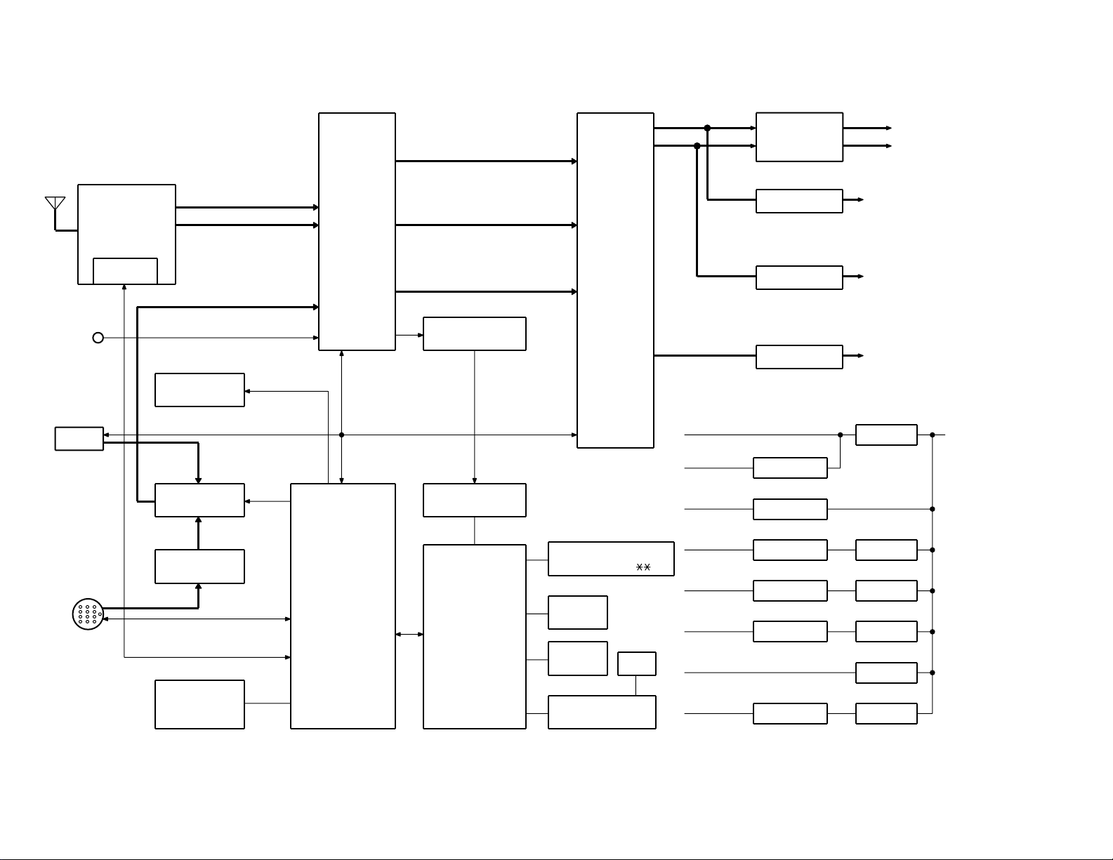
BLOCK DIAGRAM

KDC-Z828,Z828
3
● SUB-CIRCUIT UNIT (X13-9930-00)
COMPONENTS DESCRIPTION
Ref.No.
Element/Function
Operation/Condition
IC1 SYS u-COM
IC2 RESET System reset
IC3 GATE IC Gate IC for muting
IC200 GND-ISO GND-ISO for CD-CH
IC201 SW-OP CD/CD-CH input switching
IC202 Buff SA buffer and 1/2 Vdd
IC300 E-VOL/MPX E-VOL/MPX
IC301 SYSTEM E'S SYSTEM E'S
IC310-312
Buff Buffer for 4.5 V PRE-OUT
IC500 POWER AMP
IC900 PNL u-COM
IC930 REMOCON Remote control light sensor
IC940 SA BPF BPF for SA
IC950
EXTENSION ROM
IC960
3.3V POWER SUPPLY IC
3.3 V power supply
IC961 LEVEL SHIFT IC 5V-3.3 V level shifting
Q1 5V SW
Q2 MUTE SW Muting SW for PRE-OUT
Q3 CH RST SW
Q4 LED SW LED SW for DISC_ and EJ SW
Q5 PNL5V SW
Q6 PNL5V SW
Q9 Buff IFC buffer
Q10 LED SW LED SW for DSI
Q100,101
FM+B SW
Q102,103
AM+B SW
Q200 MD/CD-CH SW CD/CD-CH signal switching
Q201 MUTE DRV For SA muting
Q202 ALC ALC
Q300 MUTE E-VOL muting SW
Q350A,B
MUTE DRV PRE-OUT muting
Q351A,B
MUTE DRV PRE-OUT muting
Q352A,B
MUTE DRV PRE-OUT muting
Ref.No.
Element/Function
Operation/Condition
Q600 BU DET B-U ON/OFF detection
Q601 Acc DET Acc ON/OFF detection
Q602 P-ANT SW
Q603 P-ANT SW
Q604 P-CON SW
Q605
P-CON PROTECT
Q606
P-CON PROTECT
Q607 P-CON SW
Q608 DIMMER SW
Q609
EXT AMP CON. SW
Q610 DSP 5V AVR 5V DSP power supply
Q611,612
PNL5V AVR 5V panel power supply
Q613,614
BU5V AVR 5V uCOM power supply
Q615,616
DD-CONV SW
Q617,618
DD-CONV AVR DC/DC converter power supply
Q619,620
SURVO7.5V AVR
7.5V CD mechanism power supply
Q621,622
AUDIO8V AVR 8V Audio power supply
Q623 14V SW
8V Audio, 5 V DSP,
7.5 V SERVO and 5 V MP3 SW
Q624 14V SW
8V Audio, 5 V DSP,
7.5 V SERVO and 5 V MP3 SW
Q630 MP3 5V AVR 5V MP3 power supply
Q631 MP3 5V AVR 5V MP3 power supply
Q632,633
AUDIO DC/DC 11V Audio DC/DC CONV
11V AVR power supply
Q801-803
AUDIO -9V SW
Q804,805
AUDIO 9V SW
Q806 AUDIO 9V SW
Q900 LED SW
LED SW for SRC and KENWOOD logos
Q930,931
PNL5V SW
5V Panel SW for SA-BPF and
REMOTE-CON
Q960 BK SW
Q961,962
VFD SW

KDC-Z828,Z828
4
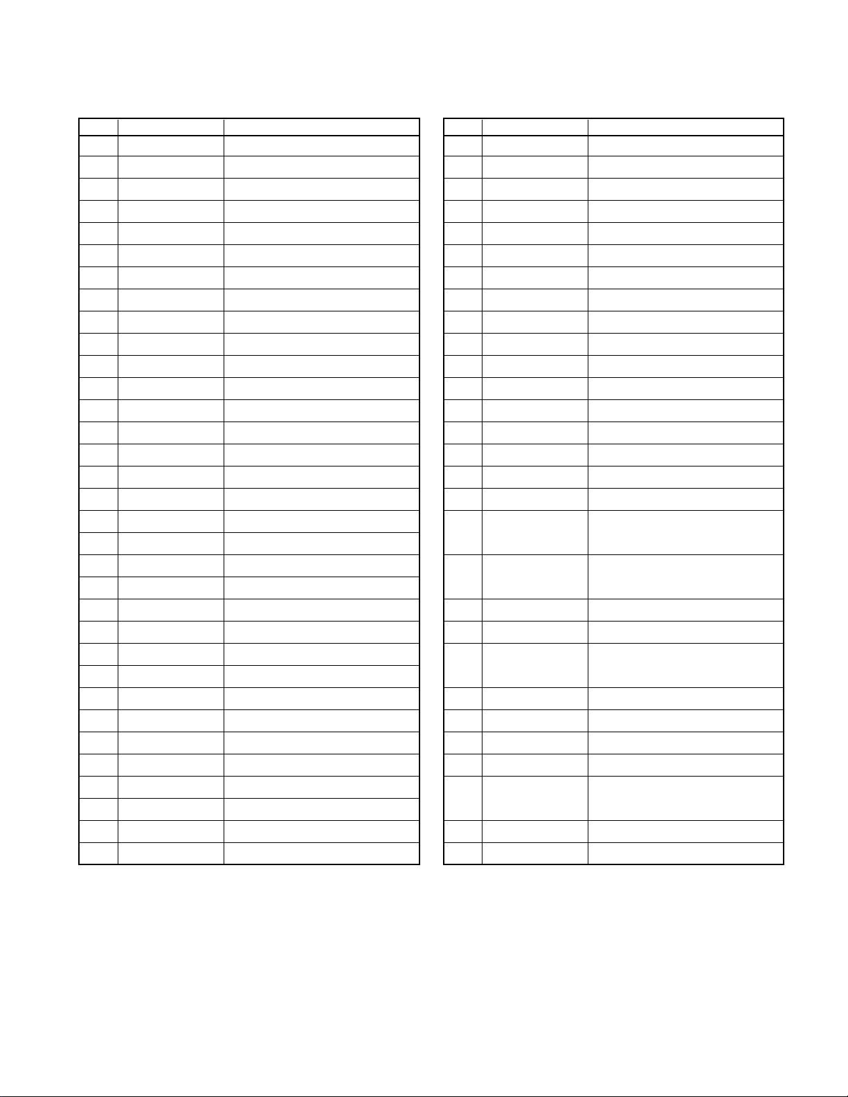
● System Microcomputer UPD703033GC060 (IC1 : Main unit)
PinNo.
Pin name I/O Description Processing Operation
1 AMP_MUTE O Muting control output to Power IC Muting ON: Low. Muting OFF: High.
2 AMP_STBY O Standby control output to Power IC
Standby canceled: High. Standby mode: Low.
3 NC O Output open
4 NC O Output open
5 P_ANT O Power antenna control output
Radio mode: High. Other mode: Low.
6 EVdd Connected to B-U 5 V
7 EVss Connected to GND
8 P_CONT O Power control output ON: High. OFF: Low.
9 BEEP O Beep output Permanently "L".
10 EXT_AMP O External amp control output
11 DIMMER I Dimmer detection input
Dimmer ON: Low. Dimmer OFF: High.
12 CH_CON O CD-CH control output ON: High. OFF: Low.
13 CH_REQH O CD-CH send request output Request: Low.
14 DSP_DATA O Data output to DSP_IC (M65849BFP)
15 DSP_STB O Strobe output to DSP_IC (M65849BFP)
16 DSP_CLK O Clock output to DSP_IC (M65849BFP)
17 NC O Output open.
18 IC/Vpp O Test
19 IN_SEL O CD/CD-CH switching control output
CD: Low. CD-CH: High. Other source: L.
20 SA_MUTE O Signal muting output to spectrum analyzer MUTE ON:HI
21 I2C_SDA I/O
Data input/output from/to CD mechanism, E-VOL (TDA7407) and HPF
22 I2C_SCK I/O
Clock output to CD mechanism, E-VOL (TDA7407) and HPF
23 MUTE O Muting control output (N-CH open drain) MUTE ON:HI, MUTE OFF:LO
24 SW5V O 5 V SW control output (N-CH open drain) SW5V ON:LO, SW5V OFF:HI
25 F/E_DATA I/O
Data input/output from/to F/E and PROM (N-CH open drain)
26 F/E_CLK I/O Clock output to F/E and PROM (N-CH open drain)
27
PRE_OUT_MUTE
O PRE-OUT muting control output
Muting ON: Low. Muting OFF: High.
Momentary power down: Low.
28 IFC I IF_COUNT input from F/E
Station detected: Low.
Station not detected: High.
29 AM+B O AM power supply control output AM ON:HI, AM OFF:LO
30 FM+B O FM power supply control output FM ON:HI, FM OFF:LO
31 RESET I Reset input LO:RESET ON
32 XT1 Connected to Sub X'tal
33 XT2 Connected to Sub X'tal
34 REGC 1 uF connected to GND.
35 X2 Connected to Main X'tal
36 X1 Connected to Main X'tal
37 Vss Connected to GND
38 Vdd Connected to B-U 5 V
39 CLKOUT Open
40 NC O Output open.
41 NC O Output open.
42 P_ON O Internal power supply control ON:HI, OFF:LO
43 VFD_ON O VFD power supply control output VFD ON:HI, VFD OFF:LO
44 NC O Output open.
PNL 5 V ON: High. PNL 5 V OFF: Low.
45 PNL5V O 5 V panel control output
Panel detached:Low. Momentary power
down: Low.
MICROCOMPUTER'S TERMINAL DESCRIPTION

KDC-Z828,Z828
5
MICROCOMPUTER'S TERMINAL DESCRIPTION
PinNo.
Pin name I/O Description Processing Operation
46 NC O
47 PNL_DET I Panel position detection input
Panel open (SW ON): Low.
Panel closed (SW OFF): High.
48 CD_MUTE I Muting input from CD mechanism MUTE:LO
49 CD_MRST O Reset output to CD mechanism RESET:LO
50 CD_MSTOP O Stop request to CD mechanism STOP:LO
51 CD_LO/EJ I/O CD mechanism loading motor control (Load/Eject) LOAD:LO EJ:HI
52 CD_LMON O CD mechanism loading motor control (ON/OFF) LOAD:LO EJ:HI
53 CD_SW3 I Input from CD mechanism SW3 (DOWN_SW input) ON:HI
54 NC O Output open.
55 BVdd Connected to B-U 5 V
56 BVss Connected to GND
57 DSI O DSI LED control output
Panel detached: ON. Panel attached: OFF.
58-64 NC O Output open.
65
PN_MC_REQ/PANEL
I/O
Send request output to Panel uCOM/Panel detection input Panel detection input. Panel ON: Low.
66 PAN_RST O Reset control output to Panel uCOM Same function as PNL 5 V.
67 LED_SW O
LED control output for EJECT SW and DISC _OUTPUT open.
ILL ON:HI, ILL OFF:LO
68,69 O Output open.
70 AVCONT O A/D reference voltage control output During operation: High.
71 AVdd Connected to B-U 5 V
72 AVss Connected to GND
73 AVref A/D reference voltage
74 PHONE I PHONE detection input
TEL muting: 1 V or less. NAVI muting: 2,5 V or more.
75-78 NC I Resistor connected to GND
79 MP3/CD I MP3/CD identification input CD: Low. MP3: High.
80 S-METER I FM S-meter input from F/E (Analog input)
81 TYPE1 I Destination type ID input
K (North America): H. M (General overseas): L
82 TYPE2 I Destination type ID input
K (North America): H. M (General overseas): H
83 NC I Resistor connected to GND
84 ST_TYPE1 I E-VOL setting selection input Normal: Low. Special: High.
85 ST_TYPE2 I E-VOL setting selection input Normal: Low. Special: High.
86 NC O Output open.
87 DISC_EJ_SW I CD EJECT SW input (Interrupt input) CD ejection: Low. (Interrupt input)
88 CH_REQC I Send request input from CD-CH (Interrupt input) ON: Low. (Interrupt input)
89 PN_SC_REQ I Send request from Panel uCOM (Interrupt input)
90 CD_SW1 I Input from CD_SW1 (Loading SW detection) LO:ON, HI:OFF
91 CD_SW2 I Input from CD_SW2 (12 cm CD detection) LO:ON, HI:OFF
92 ACC_DET I Acc detection input HI:ACC OFF, LO:ACC ON
B-U power down: High. B-U normal: Low.
93 BU_DET I B-U detection input (Interrupt input)
Muting and mechanism operation stop should
be executed quickly. (Interrupt input)
94 CH_DATAC I Data input from CD-CH
95 CH_DATAH O Data output to CD-CH
96 CH_CLK I/O Clock input/output from/to CD-CH
97 PN_SC_DATA I Data input from Panel uCOM
98 PN_MC_DATA I/O Data output to Panel uCOM
99 PN_MC_CLK O Clock output to Panel uCOM
100 NC O OUTPUT OPEN

KDC-Z828,Z828
6
● Panel Microcomputer UPD703033GC062 (IC900 : Control uCOM)
PinNo.
Pin name I/O Description Processing Operation
1 VFD_DATA1 O Data output "1" to VFD driver
2 VFD_CLK O Clock output to VFD driver
3 NC I Resistor connected to GND
4 VFD_DATA2 O Data output "2" to VFD driver
5 VFD_CLK_IN I
Clock input from VFD_CLK (For use in synchronization of DATA 1 and 2)
6 EVdd Connected to PNL 5 V
7 EVss Connected to GND
8 NC O Output open.
9 5V_ON O
Power supply control output to Remote Control IC and SA_IC.
5V ON:HI, 5V OFF:LO
10 REMO I Remote control signal input
11 NC O Output open.
12 VFD_LATCH O Latch output to VFD driver
13 VFD_GCP O Luminance gradation control output to VFD driver
14 A13 O Address output "A13" to external ROM
15 A14 O Address output "A14" to external ROM
16 A15 O Address output "A15" to external ROM
17 VFD_BLK O Blank output to VFD driver
Display ON: High. Display OFF: Low.
18 IC/Vpp Test
19 A5 O Address output "A5" to external ROM
20 A6 O Address output "A6" to external ROM
21 A7 O Address output "A7" to external ROM
22 A8 O Address output "A8" to external ROM
23 A9 O Address output "A9" to external ROM
24 A10 O Address output "A10" to external ROM
25 A11 O Address output "A11" to external ROM
26 A12 O Address output "A12" to external ROM
27 A1 O Address output "A1" to external ROM
28 A2 O Address output "A2" to external ROM
29 A3 O Address output "A3" to external ROM
30 A4 O Address output "A4" to external ROM
31 RESET I Reset input
32 XT1 Resistor connected to GND
33 XT2 OPEN
34 REGC 1 uF connected to GND
35 X2 Connected to Main X'tal
36 X1 Connected to Main X'tal
37 Vss Connected to GND
38 Vdd Connected to PNL 5 V
39 CLKOUT OPEN
40 NC O OUTPUT OPEN
41 NC O OUTPUT OPEN
MICROCOMPUTER'S TERMINAL DESCRIPTION

KDC-Z828,Z828
7
MICROCOMPUTER'S TERMINAL DESCRIPTION
PinNo.
Pin name I/O Description Processing Operation
42 NC O OUTPUT OPEN
43 OE O Output Enable output to external ROM
44 CE O Chip Enable output to external ROM
45 NC O OUTPUT OPEN
46 NC O OUTPUT OPEN
47 AD0 I Data input "AD0" from external ROM
48 AD1 I Data input "AD1" from external ROM
49 AD2 I Data input "AD2" from external ROM
50 AD3 I Data input "AD3" from external ROM
51 AD4 I Data input "AD4" from external ROM
52 AD5 I Data input "AD5" from external ROM
53 AD6 I Data input "AD6" from external ROM
54 AD7 I Data input "AD7" from external ROM
55 BVdd Connected to PNL 5 V
56 BVss Connected to GND
57 AD8 I Data input "AD8" from external ROM
58 AD9 I Data input "AD9" from external ROM
59 AD10 I Data input "AD10" from external ROM
60 AD11 I Data input "AD11" from external ROM
61 AD12 I Data input "AD12" from external ROM
62 AD13 I Data input "AD13" from external ROM
63 AD14 I Data input "AD14" from external ROM
64 AD15 I Data input "AD15" from external ROM
65 A16 O Address output "A16" to external ROM
66 A17 O Address output "A17" to external ROM
67 A18 O Address output "A18" to external ROM
68 A19 O Address output "A19" to external ROM
69 NC O OUTPUT OPEN
70 A21 O Address output "A21" to external ROM
71 AVdd Connected to PNL 5 V
72 AVss Connected to GND
73 AVref
74 SA_F01 I Spectrum analyzer signal input (63Hz)
75 SA_F02 I Spectrum analyzer signal input (150Hz)
76 SA_F03 I Spectrum analyzer signal input (330Hz)
77 SA_F04 I Spectrum analyzer signal input (1KHz)
78 SA_F05 I Spectrum analyzer signal input (3.3KHz)
79 SA_F06 I Spectrum analyzer signal input (10KHz)
80 LEVEL_M I MIX signal input for level meter
81 KR5 I Key return "5"
82 KR4 I Key return "4"

KDC-Z828,Z828
8
MICROCOMPUTER'S TERMINAL DESCRIPTION
PinNo.
Pin name I/O Description Processing Operation
83 KR3 I Key return "3"
84 KR2 I Key return "2"
85 KR1 I Key return "1"
86 PN_SC_REQ O Send request output to Main uCOM
87 AVCONT O A/D reference voltage control output Operating: High.
88 PN_SC_CON I Operation control input from Main uCOM Operating: High. (Interrupt input)
89 NC O Output open.
90 SOURCE I SRC key input
ON: High. OFF: Low. (Interrupt input)
91 BLUE O Blue LED control output LED ON:HI, LED OFF:LO
92 PN_MC_REQ I Send request input from Main uCOM
93 KS4 O Key scan "4"
94 KS3 O Key scan "3" and Flash uCOM write port
95 KS2 O Key scan "2" and Flash uCOM write port
96 KS1 O Key scan "1" and Flash uCOM write port
97 PN_SC_DATA I Data input from Main uCOM
98 PN_MC_DATA O Data output to Main uCOM
99 PN_MC_CLK I Clock input from Main uCOM
100 NC I Resistor connected to GND

KDC-Z828,Z828
9
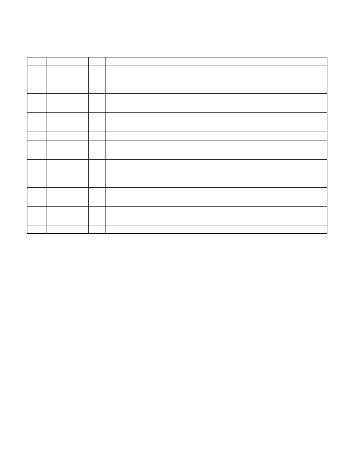
● Mechanism Microcomputer M30620MCAB12GP (IC1 : X32)
PinNo.
Pin name I/O Description Processing Operation
1-5 NC O Not used L
6 BYTE I 8-bit/16-bit path width switching H
7 CNVss I L
8,9 NC O Not used L
10 RESET I Reset terminal Reset: Low. Normal: High.
11 Xout O Clock output
12 Vss - Connected to GND
13 Xin I Clock input
14 Vcc -
15 NMI I Interrupt: Low. Normal: H.
16 INT3 I Servo DSP (processor) interrupt terminal Interrupt: Low. Normal: H.
17 INT2 I Servo DSP (decoder) interrupt terminal Interrupt: Low. Normal: H.
18 INT1 I Servo DSP (ATAPI) interrupt terminal Interrupt: Low. Normal: H.
19,20 NC O Not used L
21 DCS O DAC Chip Select L:SELECT
22 PD O Peripheral IC reset Reset: Low. Normal: High.
23 ML O Data latch line for DAC-uCOM communication Latch: High.
24 MC O Clock line for DAC-uCOM communication
25 MD O Data line for DAC-uCOM communication
26 NC O Not used L
27 I2C_CLK I/O Mechanism control communication terminal (Clock)
28 I2C_DATA I/O Mechanism control communication terminal (Data)
29 MP3_I2C_DATA I/O STA013 control communication terminal (Data)
30 R O Flash write terminal L
31 MP3_I2C_CLK I/O STA013 control communication terminal (Clock)
32 W O Flash write terminal L
33 MP3_DATA O MP3 data send terminal (Data)
34 NC O Not used L
35 MP3_CLK O MP3 data send terminal (Clock)
36 MP3_REQ I MP3 data request terminal
37 WAIT I Multiplexed path Wait terminal L:BUSY H:READY
38 ALE O Multiplexed path terminal
39 HOLD I Flash write terminal L
40 HLDA O - L
41 NC O Not used L
42 RDM O Multiplexed path terminal
43 NC O Not used L
44 WRM O Multiplexed path terminal
45 NC O Not used L
46 CS2 O M24B Chip Select L:SELECT
47-50 NC O Not used L
MICROCOMPUTER'S TERMINAL DESCRIPTION

KDC-Z828,Z828
10
PinNo.
Pin name I/O Description Processing Operation
51 SCTL O RF 1x/2x speed switching 2x: Low. 1x: High
52,53 NC O Not used
54 MUTE-R O Muting (Right) terminal Muting: Low
55 MUTE-L O Muting (Left) terminal Muting: Low
56 LDON O Laser ON/OFF terminal L:OFF H:ON
57 MP3/CD O CDDA/MP3 switching terminal L:CDDA H:MP3
58 PON O Peripheral IC power supply control terminal L:OFF H:ON
59 CDRW O RE switching terminal Other: Low. RW: High.
60 Vcc - Connected to BU 5V lines
61 NC O Not used L
62 Vss - Connected to GND
63 AD7 I/O Address/Data (Bit 7) line
64 AD6 I/O Address/Data (Bit 6) line
65 AD5 I/O Address/Data (Bit 5) line
66 AD4 I/O Address/Data (Bit 4) line
67 AD3 I/O Address/Data (Bit 3) line
68 AD2 I/O Address/Data (Bit 2) line
69 AD1 I/O Address/Data (Bit 1) line
70 AD0 I/O Address/Data (Bit 0) line
71 RFOK I RFOK interrupt terminal (Not used) Interrupt: Low. Normal: High.
72 MSTOP I MSTOP detection terminal Interrupt: Low. Normal: High.
73 INT4 I Servo DSP (servo) interrupt terminal Interrupt: Low. Normal: High.
74-78 NC O Not used L
79 T3 I Test port for electrical checking L
80 T2 I Test port for electrical checking L
81 T1 I Test port for electrical checking L
82 EMPH I Emphasis ON/OFF L:OFF H:ON
83 RFOK I RFOK terminal L:NG H:OK
84 NC O Not used L
85 SW3 I Inner edge detection switch L:ON H:OFF
86 DETECT I Detrack amount L:DETECT
87-93 NC O Not used L
94 AGND - Connected to GND
95,96 NC O Not used L
97 Avcc - Connected to BU 5V lines
98-100 NC O Not used L
MICROCOMPUTER'S TERMINAL DESCRIPTION
 Loading...