

Kenwood KD-CZ-638 Service Manual
CD RECEIVER
KDC-719/X559/Z737,Z638
SERVICE MANUAL
© 2002-3 PRINTED IN JAPAN
B51-7928-00 (N) 3382
•This service manual does not include information on the CD mechanism assembly (exploded view, parts list,
schematic diagram or mechanism operation description).
For such information, please refer to the CD mechanism assembly service manual (X92-4450-0X: B51-7889-00).
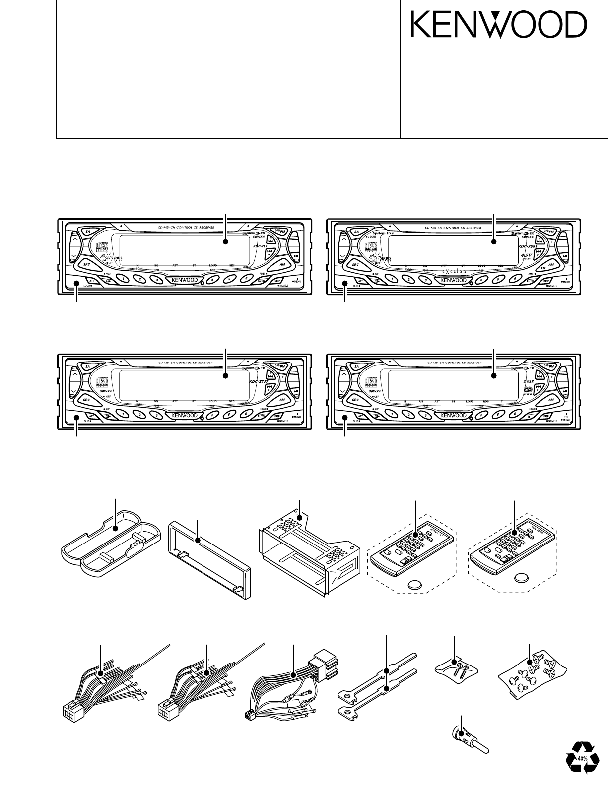
KDC-719
Panel assy
(A64-2646-11)
KDC-Z737
Panel assy
(A64-2648-11)
Plastic
cabinet assy
(A02-2712-13)
Front glass
(B10-4209-01)
Front glass
(B10-4211-01)
Escutcheon
(B07-3050-02)
: KDC-719/Z737,Z638
(B07-3057-02)
: KDC-X559
Mounting
hardware assy
(J21-9823-03)
KDC-X559
Panel assy
(A64-2650-11)
Z638
Panel assy
(A64-2647-11)
Remote controller assy
(A70-2025-05)
: KDC-719/X559
Front glass
(B10-4213-01)
Front glass
(B10-4210-01)
Remote controller assy
(A70-2026-05)
: KDC-Z737,Z638
DC cord
(E30-6062-05)
: KDC-X559/Z737
DC cord
(E30-6106-05)
: KDC-719
DC cord
(E30-6063-05)
: Z638
Lever
(D10-4674-04)x2
Antenna adaptor
(T90-0523/0534/0552-05): Z638
Screw set
(N99-1656-05)
Screw set
(N99-1723-05)
: except Z638
KDC-719/X559
CH
F/E
FM+B
PLL+B
AM+B
BUFF
E-VOL
DECODER
RDS
ISO
AMP
OEM
EJECT LED
DSI
DISP
4.5V PRE
DC/DC
2WAY MUTE
ACC DET
DIMMER
TEL-MUTE
ACC
DIMMER
POWER IC
PRE AMP
PRE OUT
SP OUT
MUTE
DRIVER
NOISE
BUFFER
ANT-CON
ANT-CON
P-CON
P-CON
IF+B
CD
MECHA
AUX
SW
OP AMP
E'S
SPEANA
AGC OP AMP
MUTE
4.5V
BU DET
BACK UP
EX AMP CONT
EX AMP CONT
NAVI MUTE
RESET
DET
PANEL
KEY ILL
MATRIX
KEY
FL
SW
MI-COM
PANEL
SPEANA
BPF
REMO
RESET
REG
SW
BUFFER
3.3V
SW
SERVO
AVR
BOX
DC/DC
A8V
SW14V
DC/DC
REG
BU5V
SW5V
PANEL5V
Q43,44
Q45,46
Q52
IC14
IC1
IC2
Q36 IC8,Q34
IC5
Q37-42
IC10-12
IC4
Q32,
IC7 33,35
Q15
Q31
Q30
Q14
Q111,112
Q26-29
Q3
Q9
IC3,Q4-6
IC6,Q16-23
Q1
A1 Q10-13
Q7,8
Q201,473-476
IC16305,306
IC1
IC5
IC2
ED1Q1,2
Q7-10
IC3
IC4
IC20
IC21
EEP ROM
IC25
Q101,
P-CON
ANT-CON
Z638 ONLY
EXCEPT KDC-X559/Z737
KDC-X559/Z737 ONLY
Z638 ONLY
Q3
EXCEPT KDC-719
Z638
ONLY
Z638 ONLY
Z638
EXCEPT
EXCEPT KDC-X559
EXCEPT KDC-X559
KDC-X559 ONLY
KDC-X559 ONLY
MI-COM
SDA
SCL
S-METER
SW5V
RDCK
FM
AM
SW5V
AUDIO OUT
BACK UP
DATA H
DATA C
MUTE
CH
SDA
RDDA
BU5V
BU5V
DSI
EJECT G
EJECT R/G
Z638 (E)
CD/MD
FM
AM
1512mV
866mV
3795mV
BU5V
PRE MUTE
PMUTE
PSTBY
MUTE
BEEP
AUX SW
CD-AUX
E-VOL OUT LEVEL
A8V
IFC OUT
SW5V
A8V
SCL
QUAL
AFS
SERVO
BU5V
Rch
Lch
A8V
A8V
A8V
REQ H
RST
REQ C
CH CON
CLK
A8V
A8V
+B
-B
BACK UP
BU5VBU5V
MC REQ
SC CON
FL+B
RED
SI2
SI1
CLK
GREEN
KS1-KS4
KR1-KR5
F01-F06
WAVE
P5V
MC CLK
SC REQ
P RST
MC DATA
GCP
LAT
P5V
REMO
FL+B
FAC
BK
P5V
A8V
+B
-B
SERVO
FAC
FL+B MI-COM
SW5V
MI-COM
BU5V
P5V
MI-COM
REMO
O- DATA
O-CE
O-CLK
1.8V PRE
613mV274mV
2005mV
3795mV
1.8V PRE
896mV
1695mV
KDC-719 (K)
4.5V PRE
AUX
CHANGER
4.5V PRE 1.8V PRE
3795mV
1512mV
866mV
896mV
274mV
1695mV
2005mV
613mV
3795mV
1.8V PRE
QUAL
E'S OUT LEVEL PRE OUT LEVEL
M RST
SW1
SW2
SW4
SW3
LO/EJ
M STOP
M SW
MUTE R
MUTE L
KDC-X559 (K)
KDC-Z737 (M)
KDC-X559 (K)
KDC-Z737 (M)
Z638 (E)
CHANGER
FM
AM
CD/MD
AUX
KDC-719 (K)
KDC-X559 (K)
KDC-Z737 (M)
Z638 (E)
AM
FM
CHANGER
AUX
CD/MD
2361mV
722mV
4.5V PRE
4469mV
848mV
1.8V PRE
1481mV
3717mV
600mV
1964mV
3717mV
1.8V PRE
KDC-719 (K)
251mV (E,M)TYPE
470mV (K)TYPE
215mV
1200mV
1200mV
2
/Z737,Z638
BLOCK DIAGRAM
KDC-719/X559
/Z737,Z638
COMPONENTS DESCRIPTION
SWITCH UNIT (X16-168x-xx)
Ref.No.
IC1 TAR5S33 FL AVR +3.3V Output
IC2 TC74HC4050AFT Buffer For FL control lines, 5V→3.3V logic level shifting
IC3 RS-171 Remote sensor IC
IC4 BA3830F BPF IC BPF for the spectrum analyser indicator
IC5 UPD703032GFA04 Panel MI-COM.
Q1 DTA144EUA or UN5113
Q2 DTC114YUA or UN5214
Q3 DTA114EUA or UN5111 REMO SW
Q4 DTC114EUA or UN5211 FL blanking SW When a base goes Hi, Q4 is turned on, and FL indicator is lit.
Q6 DTC114YK or UN2214 SRC key illumination SW When a base goes Hi, Q6 is turned on, and SRC illumination is lit.
Q7 2SC4081 V-I converter Current driver for green LEDs
Q8 2SC4081 V-I converter Current driver for red LEDs
Q9 DTA114EUA or UN5111 Key illumination Red SW When a base goes Lo, Q9 is turned on, and key illumination Red is lit.
Q10 DTA114EUA or UN5111 Key illumination Green SW
Component Name Application/Function Operation/Condition/Compatibility
FL+B SW
FL & Illumination +B ON/OFF control. When Q2's base goes Hi, Q1 is turned on,
and FL+B (45V) line is supplied to FL indicator and the key illumination circuit.
When a base goes Lo, Q3 is turned on, and PAN5V line is supplied to
IC3 and IC4.
When a base goes Lo, Q10 is turned on, and key illumination Green is lit.
ELECTRIC UNIT (X25-924x-xx)
Ref.No.
IC1 UPD703033GFA18 System MI-COM.
IC2 TDA7407 E-VOL.& N.C. MPX
IC3 M5237ML AVR IC
IC4 TDA7560 Power IC
IC5 TDA7401
IC6 ICL7660SIBA DC/DC converter -9V AVR for pre-output amplifier
IC7 TC74HC02AF Mute logic 2-input NOR x 4
IC8 NJM4565M-TE2 Op. amp.
IC10 NJM4565M-TE2 Op. amp. Amplifier for the front pre-outputs
IC11 NJM4565M-TE2 Op. amp. Amplifier for the non-fader pre-outputs
IC12 NJM4565M-TE2 Op. amp. Amplifier for the rear pre-outputs
IC14 TDA7479D RDS decoder
IC16 S-80837ANNP Reset IC When BU 5V voltage is less than 3.7V, IC outputs Lo.
IC20 BA3121F Isolation amplifier AUX inputs isolation amplifier
IC21 BA3129F Switched op.amp. Input switching with AUX inputs and CD inputs
IC25 BR24C02F-W EEPROM
Q1 2SD2375 CD servo AVR AVR for CD mechanism servo operation, +7.5V output.
Q3 2SA1037K SW 5V
Q4 2SA2057 A.+8V AVR
Q5 DTC144EUA or UN5213
Q6 DTA124EUA or UN5112
Q7 DTA124EUA or UN5112
Q8 DTC124EUA or UN5212 AVR and A+10V AVR are working.
Q9 2SB1427 PAN5V SW
Q10 2SA2057
Q11 2SC4081
Component Name Application/Function Operation/Condition/Compatibility
IC is combined with Q4, and it works as the error detection, the Q4's driver.
High pass filter & Non-Fader
volume
A.+8V AVR SW When Q5's base goes Hi, Q6 is turned on, and A.+8V AVR is working.
SW14V
FL/Illumination AVR When Q11's base goes Hi, AVR outputs +9V.
HPF (Front/Rear output), LPF, Non-Fader switching and volume function
Amplifier for the spectrum analyser and generation of Vref. (1/2Vcc) voltage
While a base goes Lo, SW 5V is supplied to the microprocessor
peripheral circuits.
Q4 is combined with IC3, and it works as the power supply of +8.0V output.
When Q8's base goes Hi, Q7 is turned on, and A.+8V AVR, CD servo
For PAN5V on/off switching. When a base goes Lo with panel attached
to the set, Q9 is turned on, and PAN5V is supplied to the panel.
3
KDC-719/X559
/Z737,Z638
COMPONENTS DESCRIPTION
Ref.No.
Q12 DTC124EUA or UN5212
Q13 DTA124EUA or UN5112
Q14 DTA123JK or KRA105S EXT. AMP CON. SW
Q15 DTC144EUA or UN5213 Dimmer detection SW
Q16 2SB1443
Q17 2SC4081
Q18 2SA1576A
Q19 2SC4081 PRE-AMP -9V AVR
Q20 2SA1576A
Q21 2SC4081
Q22 2SC4081 PRE-AMP +9V AVR
Q23 2SA1576A
Q26 2SB1277(Q,R)
Q29 DTC114YUA or UN5214 Works during POWER ON mode.
Q27 2SA1576A P-CON. protection SW Protect Q26 by turning ON when P-CON output is grounded.
Q28 DTA124EUA or UN5112 P-CON. protection inhibit SW Prevents Q27 tuning ON during star t-up after power ON.
Q30 2SC4081 BU detection SW When momentary power down has detected, a base goes Lo, and Q30
Q31 2SC4081 ACC detection SW While ACC is applied, a base goes Hi, and Q31 is turned on.
Q32 DTA124EUA or UN5112 Mute driver for R Ch. When BU detection SW or System RESET or MI-COM.'s MUTE is
Q33 DTA124EUA or UN5112 Mute driver for L Ch. working, a base goes Lo, and Q32 and Q33 are turned on.
Q34 2SC4081 AGC for spectrum analyser
Q35 DTC124EUA or UN5212 E. VOL. mute SW
Q36 DTC143TUA or UN5216 Noise buffer
Q37 DTC143TUA or UN5216 Audio mute SW (Front L) When Q37's base goes Hi, Pre-output is muting.
Q38 DTC143TUA or UN5216 Audio mute SW (Front R) When Q38's base goes Hi, Pre-output is muting.
Q39 DTC143TUA or UN5216
Q40 DTC143TUA or UN5216
Q41 DTC143TUA or UN5216 Audio mute SW (Rear L) When Q41's base goes Hi, Pre-output is muting.
Q42 DTC143TUA or UN5216 Audio mute SW (Rear R) When Q42's base goes Hi, Pre-output is muting.
Q43 DTC124EUA or UN5212
Q44 CPH3105 the F/E. Works during FM reception mode or RDS reception mode.
Q45 DTC124EUA or UN5212
Q46 CPH3105 the F/E. Works during AM reception mode.
Q52 DTC143TUA or UN5216 Composite signal buffer
Q101 DTA114YUA or UN5114 DSI LED SW When a base goes Lo, Q101 is turned on, and DSI illumination LED is lit.
Q103 DTC124EUA or UN5212 AUX/CD selector SW
Q111 2SB1277(Q,R)
Q112 DTC114YUA or UN5214 Works during FM/AM reception mode or RDS reception mode.
Q201 2SC4081 BU5V discharge SW
Q305 DTA114YUA or UN5114 EJECT LED Red SW
Q306 DTA114YUA or UN5114 EJECT LED Green SW
Q473 2SC4081
Q474 2SB1548(P) Q473 and Q474 are inverted Darlington connection.
Q475 2SC4081
Q476 2SB1548(P)
Component Name Application/Function Operation/Condition/Compatibility
FL/Illumination AVR SW
A.+10V AVR When Q17's base goes Hi, AVR outputs +10V.
P-CON SW
Audio mute SW (Non Fader R)
Audio mute SW (Non Fader L)
FM+B SW
AM+B SW
P-ANT SW
BU 5V AVR
Voltage converter
When Q12' base goes Hi, Q13 is turned on, and FL/Illumination AVR is working.
When a base goes Lo, Q14 is turned on, and control pulse signal is outputted.
When vehicle small lamps turn on, Q15's base goes Hi, and it is turned on .
Q18 and Q20 work as a differential amplifier, Q19 works as a driver, and
-9.3V is supplied to OP AMP.
Q21and Q22 work as a differential amplifier, Q23 works as a driv er, and
+9.7V is supplied to OP AMP.
When Q29's base goes Hi, Q26 is turned on, and P-CON signal is outputted.
While BACKUP is applied, a base goes Hi, and Q30 is turned on.
is turned off.
When BU detection SW or MI-COM.'s mute is working, a base goes Hi,
and Q35 is turned on.
When Q39's base goes Hi, Pre-output is muting.
When Q40's base goes Hi, Pre-output is muting.
When Q43's base goes Hi, Q44 is turned on, and A.+8V is supplied to
When Q45's base goes Hi, Q46 is turned on, and A.+8V is supplied to
When a base goes Hi, AUX inputs are selected.
When a base goes Lo, CD inputs are selected.
When Q112's base goes Hi, Q111 is turned on, and P-ANT signal is outputted.
When BU OFF is detected, Q201 is turned on during the base Hi condition.
When a base goes Lo, Q305 is turned on, and EJECT illumination LED is lit.
When a base goes Lo, Q306 is turned on, and EJECT illumination LED is lit.
While BACKUP is applied, AVR outputs +5V.
Q475 and Q476 work as voltage coverter for BU 5V AVR, and it output +9V.
4
KDC-719/X559
MICROCOMPUTER’S TERMINAL DESCRIPTION
IC5 (SWITCH UNIT: X16-168x-xx)
Pin No.
1 SC DATA I/O Data input/output with the system MI-COM.
2 MC CLK I Clock input from the system MI-COM.
3 NC O Not used (N.C.)
4 DATA 1 O Data output 1 to the FL driver IC
5 CLK O Clock output to the FL driver IC (Data shift by the rise edge of the pulse)
6 NC O Not used (N.C.)
7 DATA 2 O Data output 2 to the FL driver IC
8 CLK IN I Clock input from the FL driver IC (Data shift by the rise edge of the pulse)
9 EVDD - Positive power supply connection terminal Connected to P5V lines.
10 EVSS - Ground connection terminal Connected to GND lines.
11 RED LED O
12 GREEN LED O colours
13 REMO I Data input from the remote control light sensor
14 LATCH O Latch output to the FL dr iver IC Lo: Latch, Hi: Through
15 GCP O Control pulse output to the FL brightness
16 REMO ON I/O
17-19 NC O Not used (N.C.)
20 BLK O Display ON/OFF control output Lo: Display OFF, Hi: Display ON
21 TEST I Test terminal Not used (Connected to GND lines)
22-33 NC O Not used (N.C.)
34 RESET I Reset terminal Lo: Reset, Hi: Reset release
35 XT1 - Sub clock resonator connection terminal Not used (Pull down to GND lines)
36 XT2 - Sub clock resonator connection terminal Not used (N.C.)
37 REGC -
38 X2 - Main clock resonator connection terminal
39 X1 - Main clock resonator connection terminal
40 VSS - Ground connection terminal Connected to GND lines.
41 VDD - Positive power supply connection terminal Connected to P5V lines.
42-47 NC O Not used (N.C.)
48 FL +3.3V O FL VDD ON/OFF output Lo: OFF, Hi: ON
49 FL+B I/O FL+B ON/OFF output Hi-Z: OFF, Hi: ON
50-55 NC O Not used (N.C.)
56 BLUE LED I/O Source key LED ON/OFF output Hi-Z: OFF, Hi: ON
57 NC O Not used (N.C.)
58 BVDD - Positive power supply connection terminal Connected to P5V lines.
59 BVSS - Ground connection terminal Connected to GND lines.
60-71 NC O Not used (N.C.)
Pin Name I/O Description Processing Operation
Illumination red ON/OFF output in case of two colours
/Illumination ON/OFF output in case of one colour
Illumination green ON/OFF output in case of two
/Not used in case of one colour
Power supply ON/OFF output to the remote control
light sensor IC and BPF IC
Capacitor connection terminal for regulator inside
microprocessor
Lo: ON, Hi: OFF
Lo: ON, Hi: OFF in case of two colours
/Not used (N.C.) in case of one colour
Lo: ON, Hi-Z: OFF
/Z737,Z638
5
KDC-719/X559
/Z737,Z638
MICROCOMPUTER’S TERMINAL DESCRIPTION
Pin No.
72 SA RESET O Reset output to the BPF IC Hi: Reset
73 NC O Not used (N.C.)
74 AVDD 75 AVSS - A/D converter ground connection terminal Connected to GND lines.
76 AVREF - A/D converter reference voltage input terminal
77 F01 I BPF (63Hz) input
78 F02 I BPF (150Hz) input
79 F03 I BPF (330Hz) input
80 F04 I BPF (1kHz) input
81 F05 I BPF (3.3kHz) input
82 F06 I BPF (10kHz) input
83 WAVE IN I Audio input
84 KR5 I Key return 5 input
85 KR4 I Key return 4 input
86 KR3 I Key return 3 input
87 KR2 I Key return 2 input
88 KR1 I Key return 1 input
89 SC REQ O
90 NC O Not used (N.C.)
91 SC CON I Control input from the system MI-COM. Hi: Operation mode
92 NC O Not used (N.C.)
93 SOURCE I Source key input Lo: Key OFF, Hi: Key ON
94 VREF CON O A/D converter reference voltage control output Hi: Active, Connected to AVREF terminal
95 MC REQ I
96 KS4 I/O Key scan output 4
97 KS3 I/O Key scan output 3
98 KS2 I/O Key scan output 2
99 KS1 I/O Key scan output 1
100 MC DATA I Data input from the system MI-COM.
Pin Name I/O Description Processing Operation
A/D converter positive power supply connection terminal
Communication request output to the system MI-COM.
Communication request input from the system MI-COM.
Connected to P5V lines.
Lo: Standby, Hi: Request
Hi: Request
IC5 (ELECTRIC UNIY: X25-9240-xx)
Pin No.
1 MC DATA I/O Data input/output with the panel MI-COM.
2 MC CLK O Clock output to the panel MI-COM.
3 DSI GUIDE I/O DSI control output
4 EJECT KEY G O Eject key illumination green control output Lights on at the panel tilted during POWER ON
Pin Name I/O Description Processing Operation
Lo: DSI ON, Hi-Z: DSI OFF
Lights on at the panel tilted dur ing POWER ON mode.
Flashing at the panel detached during POWER ON mode.
Lo: ON, Hi-Z: OFF
mode in case of the key illumination green.
6
KDC-719/X559
/Z737,Z638
MICROCOMPUTER’S TERMINAL DESCRIPTION
Pin No.
5 EJECT KEY R/G O Eject key illumination red/green control output
6 MC REQ/FLIP DET I/O
7 IC2 SDA I/O Data input/output with IC2, IC5, and IC25
8 IC2 SCL I/O Clock input/output with IC2, IC5, and IC25
9 EVDD - Positive power supply connection terminal Connected to BU 5V lines.
10 EVSS - Ground connection terminal Connected to GND lines.
11 PAN RESET O Reset output to the panel MI-COM. Lo: Reset or Momentary power down detected
12 BEEP O BEEP output
13 REMO I Data input from the wired remote control
14 SVR O SVR output Not used (N.C.)
15 DIMMER I Small lights detection input Lo: During vehicle small lamps turn on
16 PLL DATA I/O Data input/output with F/E
17 PLL CLK I/O Clock input/output with F/E
18 P-STBY O POWER IC STBY output
19 P-CON I/O P-CON output
20 ANT-CON O ANT-CON output
21 TEST - Test terminal Not used (Connected to GND lines)
22 P MUTE O POWER IC mute output
23 PAN5V I/O Panel 5V control output
24 EXT-AMP-CON O External amp. control output (in 200msec) Bass boost LOW__Hi: 130msec, Lo: 70msec
25 CD MECHA+B I/O CD4.7V ON/OFF output Not used (N.C.)
26 EMUTE O Not used (N.C.)
27 BU DET I Momentary power down detection input
28 ACC DET I ACC detection terminal Lo: ACC ON, Hi: ACC OFF
29 SW5V I/O SW5V control terminal Lo: SW5V ON, Hi-Z: SW5V OFF
30 MUTE I/O MUTE output Lo: Muting OFF, Hi-Z: Muting ON
31 O CE I/O External display CE terminal
32 O CLK I/O External display clock terminal
33 O DATA I/O External display data terminal
34 RESET I Reset input Lo: System reset , Hi: Normal operation
35 XT1 I Sub clock resonator connection terminal Clock count during POWER OFF mode
36 XT2 - Sub clock resonator connection terminal
Pin Name I/O Description Processing Operation
Lo: ON, H-Z: OFF
Lights on at the panel tilted during POWER ON mode.
Communication request output to the panel MI-COM.
/Flip detection input /Lo: Panel detected, Hi: Panel attached
Hi: Request
Lo: Power IC OFF, Hi: Power IC ON or ALL OFF
mode
Hi-Z: POWER OFF mode or ALL OFF mode,
Hi: POWER ON mode
Hi: During TUNER mode or last FM mode with
RDS/RBDS model
Lo: Muting during POWER OFF mode, ALL OFF
mode and TEL MUTE ON
Lo: Panel attached normally, Hi-Z: Panel detached
or tilted
Bass boost OFF__Hi: 160msec, Lo: 40msec
Bass boost HI__ Hi: 100msec, Lo: 100msec
Lo: BU ON, Hi: When momentary power down
detected or BU OFF
7
KDC-719/X559
/Z737,Z638
MICROCOMPUTER’S TERMINAL DESCRIPTION
Pin No.
37 REGC -
38 X2 - Main clock resonator connection terminal
39 X1 I Main clock resonator connection terminal
40 VSS - Ground connection terminal Connected to GND lines.
41 VDD - Positive power supply connection terminal Connected to BU 5V lines.
42 CLKOUT O Internal system clock output Not used (N.C.)
43 NC O Not used (N.C.)
44 E2PDET I EEPROM detection input Lo: No EEPROM, Hi: With EEPROM
45 PRE MUTE L O Pre-out muting L Ch. control output selected or Momentary power down detected, Hi:
46 PRE MUTE R O Pre-out muting R Ch. control output selected or Momentary power down detected, Hi:
47 DSP DATA O Data output to DSP IC Not used (N.C.)
48 DSP LATCH O Latch output to DSP IC Not used (N.C.)
49 DSP CLK O Clock output to DSP IC Not used (N.C.)
50 AFS O Noise detection time constant switching terminal FM reception, Hi: During last FM mode with
51 AM+B I/O AM+B control Hi: During AM reception
52 FM+B I/O FM+B control
53 R QUAL I Quality input from the RDS decoder IC
54 R DATA I Data input from the RDS decoder IC
55 IC2TYPE0 I IC2 setting ter minal Lo: Initial value (default)
56 IC2TYPE1 I IC2 setting ter minal Lo: Initial value (default)
57 P ON I/O SW 14V control output Hi-Z: POWER OFF mode, Hi: POWER ON mode
58 BVDD - Positive power supply connection terminal Connected to BU 5V lines.
59 BVSS - Ground connection terminal Connected to GND lines.
60 TYPE0 I Destination type selection terminal 0
61 TYPE1 I Destination type selection terminal 1
62 TYPE2 I Destination type selection terminal 2
63 TYPE3 I Destination type selection terminal 3
64 AUX SW O CD/AUX input switching output Lo: Except AUX input, Hi: AUX input
65 ILL ON I/O FL/Illumination AVR ON/OFF control output Hi-Z: AVR OFF, Hi: AVR ON
66 MOSW O CD mechanism loading motor control output Hi: CD loading/eject action or Break, Lo: Other
67 LO/EJ I/O CD mechanism loading/Eject switching output Lo: Loading, Hi: Eject, Hi-Z: Stop or Break
Pin Name I/O Description Processing Operation
Capacitor connection terminal for regulator inside
microprocessor
Oscillation: POWER ON mode, Oscillation stop:
POWER OFF mode or momentary power down detected
Lo: When M MUTE L input is Lo during CD source
Fix in the case of 2 zone mode
Lo: When M MUTE R input is Lo during CD source
Fix in the case of 2 zone mode
Lo: During FM seek or AF search, Hi: During
RDS/RDBS model
Hi: During FM reception, Hi: During last FM mode
with RDS/RDBS model
Except RDS, RBDS model: Not used (pull down to
GND lines)
Except RDS, RBDS model: Not used (pull down to
GND lines)
8
KDC-719/X559
/Z737,Z638
MICROCOMPUTER’S TERMINAL DESCRIPTION
Pin No.
68 M STOP O Stop request to CD mechanism MI-COM. Lo: Stop mode, Hi: Oper ation mode
69 M RST O Reset output to CD mechanism MI-COM. Lo: Reset
70 CH CON O Changer control Lo: Standby mode, Hi: Operation mode
71 CH RST O Reset output to changers : Reset
72 CH REQH O Request output to changers Lo: Request
73 AVCONT O A/D converter reference voltage control output Hi: Active, Connected to AVREF terminal
74 AVDD -
75 AVSS - A/D converter ground connection terminal Connected to GND lines.
76 AVREF I A/D converter reference voltage input terminal
77 IFC OUT I F/E IFC OUT input terminal Hi: Station detected (Vth=2.5V)
78 S METER I S-meter input from F/E
79 NOISE I FM noise detection input
80,81 NC I Not used (Pull down to GND lines)
82 CD SW2 I 12cm disc detection SW input Lo: 12cm disc detected
83 M MUTE R I
84 M MUTE L I
85 CD SW3 I Down & limit switch detection input Hi: Chucking, Hi→Lo: Pickup most inner position
86 PANEL DET I Panel detection input Lo: Panel attached, Hi: Panel detached
87 CH MUTE I Mute request from changers Hi: Mute request
88 PHONE I PHONE detection input
89 SC CON O Control output to the panel MI-COM. Hi: Operation mode
90 SOURCE I/O SOURCE key detection input Not used (N.C.)
91 CD SW1 I Loading SW detection input Lo: Loading start
92 CD SW4 I/O 8cm disc detection SW input Not used (N.C.)
93 R CLK I Clock input from the RDS decoder IC
94 CH REQC I Communication request input from changers Lo: Request
95 EJECT I EJECT key detection input Lo: When EJECT key is pressed
96 SC REQ I
97 CH DATAC I Data input from changers
98 CH DATAH O Data output to changers
99 CH CLK I/O Clock input/output with changers
100 SC DATA I Data input from the panel MI-COM.
Pin Name I/O Description Processing Operation
A/D converter positive power supply connection
terminal
Mute request (R Ch.) from CD mechanism MI-COM.
Mute request (L Ch.) from CD mechanism MI-COM.
Communication request input from the panel MI-COM.
Connected to BU 5V lines.
Lo: Mute request
Lo: Mute request
1V or less: TEL MUTE, 2.5V or greater: NAVI
MUTE
Except RDS, RBDS model: Not used (pull down to
GND lines)
Hi: Request
9
 Loading...