Kenwood KD-CCX-89 Service Manual
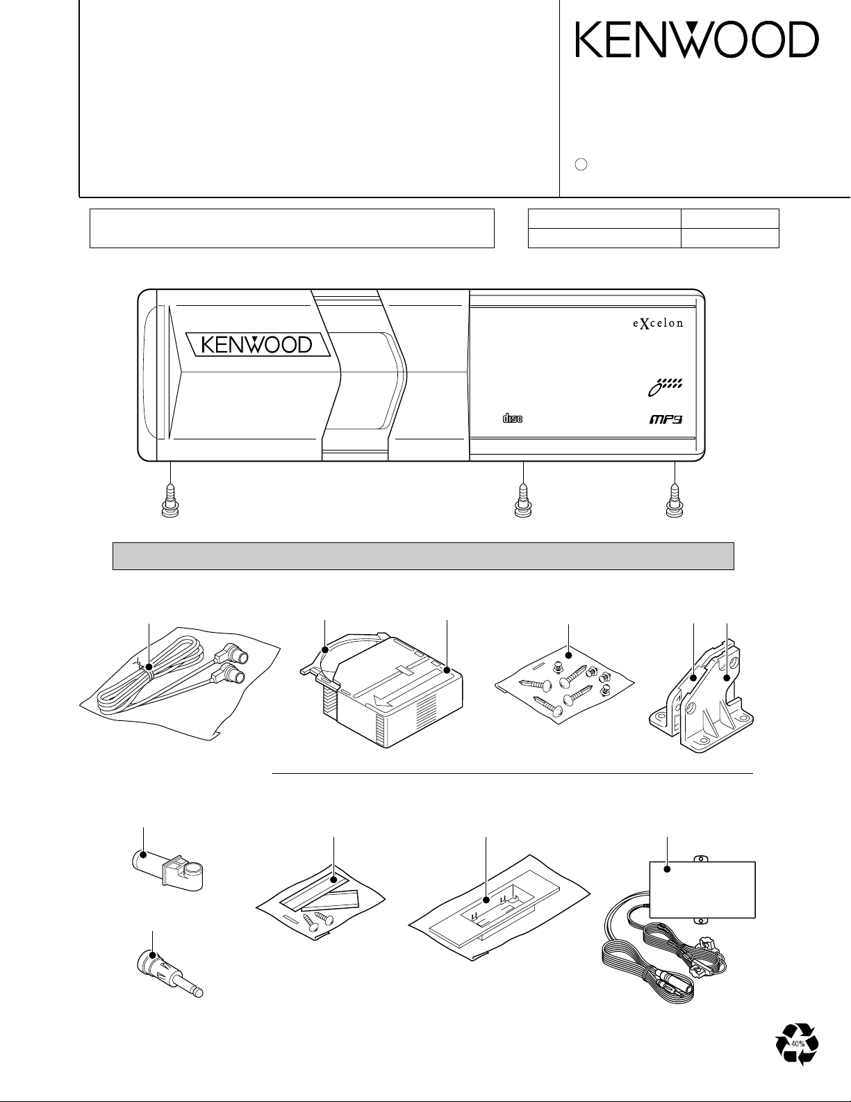
CD AUTO CHANGER
KDC-CX89/CMP59FM
KDC-CPS89MP/C719MP
C
SERVICE MANUAL
2002-2 PRINTED IN JAPAN
B51-7896-00 (4) 3404
The MECHANISM OPERATION is the same as model KDC-C660.
Please refer to the service manual of model KDC-C660 (B51-7105-00).
Service jig Parts No.
For initial position setting W05-0635-00
•KDC-CX89
10
COMPACT DISC AUTO CHANGER KDC-CX89
NEW ANTI VIBRATION MECHANISM
COMPACT
CD-R/RW
DIGITAL AUDIO
STEPPED SCREW
(N09-4383-05)
When transporting these models, always attach CAUTION CARD and STEPPED SCREW (for transportation).
CORD WITH PLUG
(E30-4291-05)
TRAY
(J99-0612-01)
HOLDER ASSY
(J19-5074-02)
SCREW SET
(N99-1645-15)
DISC
1 BIT-4 D/A CONVERTER
BRACKET (L)
(J19-5018-03)
BRACKET (R)
(J19-5019-03)
For KDC-CMP59FM
ANTENNA ADAPTOR
(T90-0521-05)
ANTENNA ADAPTOR
(T90-0512-05)
MAGICTAPE ASSY
(W01-0763-08)
HOLDER ASSY
(B07-2138-08)
CASE
(A01-2723-08) (K1)
(A01-2695-08) (E2)

2
KDC-CX89/CMP59FM/C719MP/CPS89MP
(X92)
(X32)
PICKUP
ASSY
PD
D
A
C
B
FE
FO COIL
TR COIL
SPINDLE/LO-EJ
M
SLED
M
(X13)
LOE SW
LIM SW
ELEVATOR
M
SW+3.3V
IC3
8
BTL
DC MOTOR
DRIVER
IC1
RF AMP & SERVO DSP
CD-ROM DECODER
MP3 DECODER
DAC
7
APC
SRV+8V
4
A+3.3V
X1
16.9344MHz
IC6
X3
16MHz
SW+5V
IC2
D-RAM
Q16-19
IC7
A+8V
IC4
L.P.F.
IC8
LEVEL
SHIFTER
IC5
5
MECHA
CONTROL
u-COM
BU+5V
S1
MG SW
EJ SW
PON5V
X2
12.5MHz
S2
6
AUDIO
MUTE
2
EEP-ROM
2
SW+3.3V
3
SYSTEM
CONTROL
u-COM
SW+3.3V
HOT
BU+5V
SW+5V
PON5V
SRV+8V
IC12
DELAY
A+3.3V
6
IC11
3.3V REG
A+8V
IC9
BU+5V
SW
3.3V
REG
Q11
Q9
Q7
7-8.5V REG
& SW
SW
Q2
BU DETECT
5V REG
5V REG
& SW
AUDIO
OUT
BU14V
CHCLK
REQH
REQC
DATAH
DATAC
CH CON
CH RST
CH MUTE
BLOCK DIAGRAM
S3
ARM SW
COMM SW
SW+5V
S4
LPS
IC10
RESET
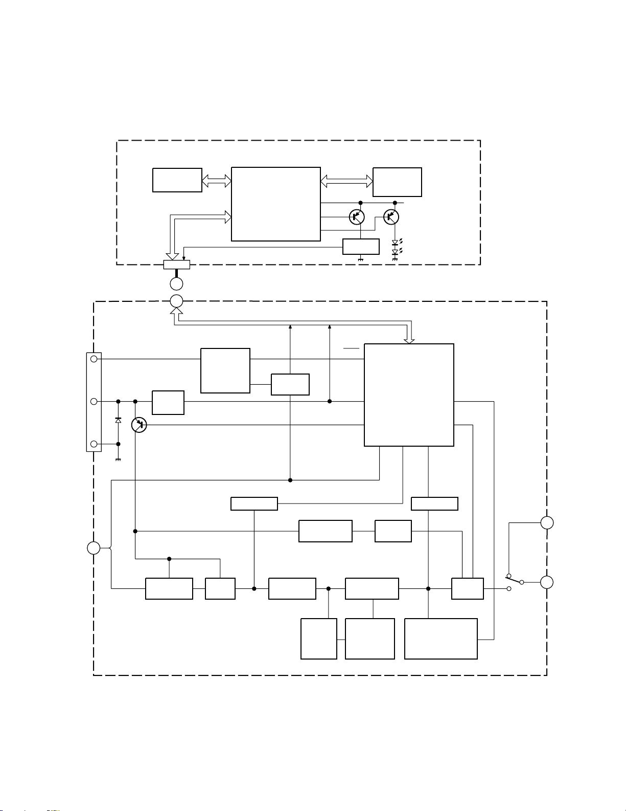
For KDC-CMP59FM
KDC-CMP59FM
BLOCK DIAGRAM
DISPLAY
ACC
BATT
GND
CN103
KEY MATRIX
CN1
IC1
AVR
(+5V)
CN101
Q1,6
IC1
2,50-56
19-22,32,66
ACC
DETECTION
6-43
LCD DRIVER
3
1
RF MODULATOR
Q4,5
RESET
DRIVER
LCD1
VDD
IC2
REMOTE
SENSOR
IC2
HOLD
VDD
P ON PLL
19-22,32,66
67
u-COM
31
63
12-17 26 61
29,30,60
74,77
CD-CH
13P
CN102
SIGNAL
(L/R)
+V(RF STAGE)
+V(AUDIO)
IC101
ISOLATION
AMP. L.P.F.
2nd.
Q308
MODE 1,2
IC102
IC4
AVR(+5.6V)
EMPHASIS
Q101,201
ALC
DRIVER
CH-CONTROL
IC301
FM-St.
MODULATOR
IC302
ALC
DETECTION
AMP
RIPPLE
FILTER
MPX
Q310
MODE 1,2
Q306,
PILOT
MIX
307
RF
STAGE
Q304,305
LEVEL CONTROL
Q309
AUDIO MUTE
RL1
CN104
ANT IN
CN105
To
RADIO
3
KDC-CX89/CMP59FM/C719MP/CPS89MP
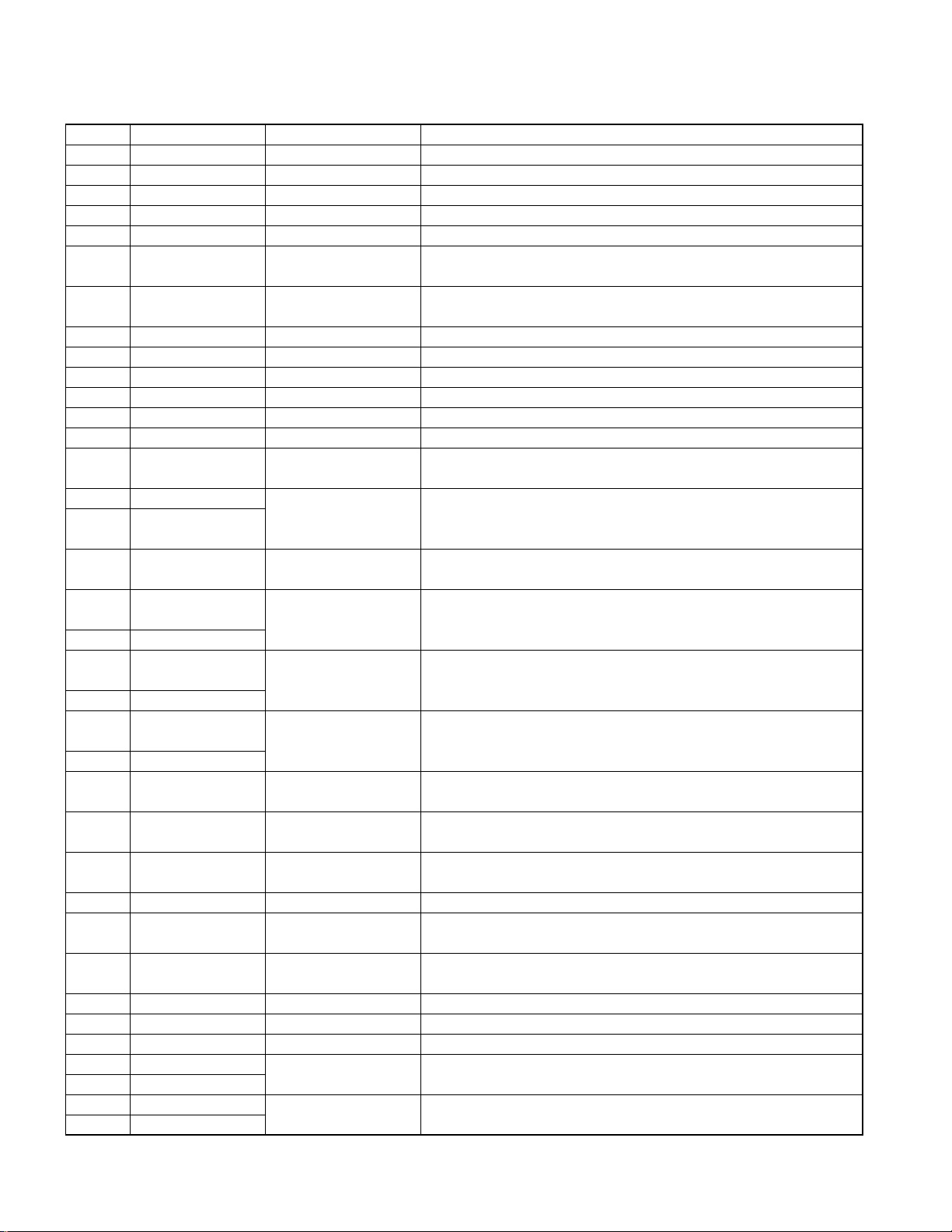
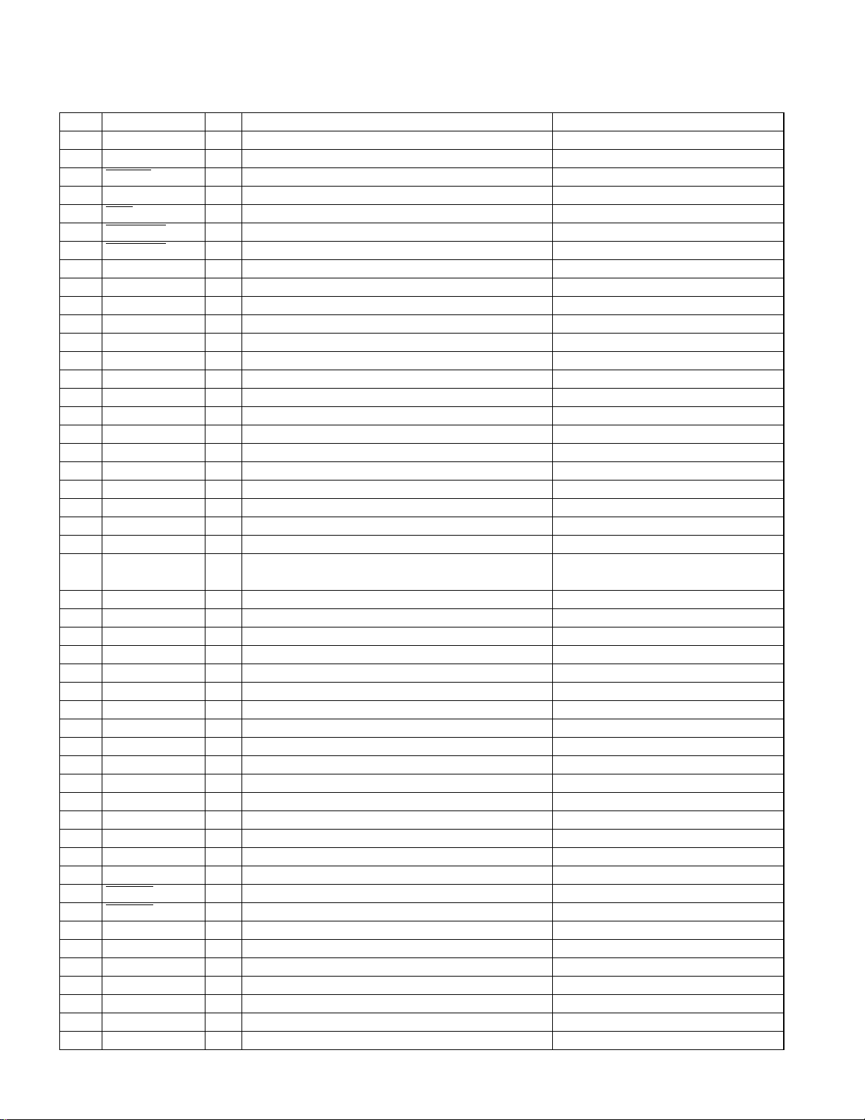
COMPONENTS DESCRIPTION
CD PLAYER UNIT (X32-5340-00)
•
Ref No.
IC1
IC2
IC3
IC4
IC5
IC6
IC7
IC8
IC9
IC10
IC11
IC12
Q1
Q2
Q3
Q4
Q5
Q6
Q7
Q8
Q9
Q10
Q11
Q12
Q13
Q14
Q15
Q16
Q17
Q18
Q19
Q20
Q21
Q22
Q23
Q24
Component Name Application/Function Operation/Condition/Compatibility
UPD63760GJ
UPD784214GC144
LA6576
NJM4580M1
703033AYGC-J01
IS41LV16257 or
MSM51V4265EP70
BR24C01AF-W or
M24C01-WMN6T
TC74HCT7007AF
TAR5S33
S-80830ANNP
L88M33T
TC7SH32FU
MCH6101
DTC124EUA or
UN5212
DTA143EUA
DTC124EUA
UN5212
DTC124EUA
UN5212
2SC4081
2SD1819A
2SB1548(P)
2SC4081
2SD1819A
2SB1548(P)
2SC4081
2SD1819A
2SB1202
DTC124EUA
UN5212
DTC124EUA
UN5212
DTC124EUA
UN5212
DTA143EUA
DATA124EUA
UN5112
DATA124EUA
UN5112
DTC343TK
DTC343TK
2SB1295
DATA143EUA
DTC124EUA
2SB1295
UN5212
SERVO IC
SYSTEM
MOTOR DRIVER
AUDIO AMP
MECHA
D-RAM
EEPROM
LEVEL SHIFTER
POWER SUPPLY IC
RESET IC
3-PIN REGULATOR
LOGIC IC
APC TRANSISTOR
BU DETECTION
SERVO 8V SW
7/9V SW
SERVO 8V AVR
PON 5V AVR
BU 5V AVR
MUTE DRIVER
CH-RST SW
CH-CON SW
CH-MUTE SW
0bit MUTE
0bit MUTE
0bit MUTE
0bit MUTE
SW 5V SW
PON 5V SW
AUDIO 8V SW
µ
µ
-COM
-COM
Controls the actuator and drives the motor.
LPF
MD deck ascent/descent home position memory
Audio system 3.3V power supply
System microcomputer reset
Digital system 3.3V power supply
Creates the audio system power supply timing
Controls the laser current
7/9V switching control
Rch
Lch
Lch
Rch
4
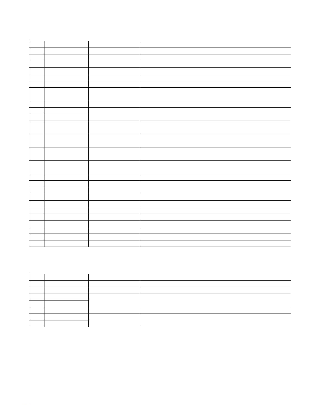
RF MODULATOR UNIT
•
Ref No.
IC101
IC102
IC301
IC302
Q101
Q201
Q303
Q304
Q305
Q306
Q307
Q308
Q309
Q310
Component Name Application/Function Operation/Condition/Compatibility
IC1
UPC7805AHF
IC2
LC72329-9274
IC4
NJM78L05UA
NJM2060M
NJM4565MD
BA1405F
NJM4565MD
Q1
DTC124EK
Q2
2SA1782(T,U)
Q3
DTC124EK
Q4
DTC143TK
Q5
DTC143TK
Q6
DTA124EK
Q8
DTC143TK
Q9
2SC4640(T,U)
2SK2158
2SK2158
2SA1162(GR)
2SK2158
2SK2158
2SK508L
2SC2714(Y)
2SK2158
2SK2158
2SK2158
COMPONENTS DESCRIPTION
BU 5V AVR
System MI-COM.
5V AVR
Isolation amp.
Low pass filter
FM ST modulator
1/2 VCC driver,
ALC detection amp.
ACC detection
POWER SW
Reset SW
CH RESET SW
Hold detection SW
Relay driver
Ripple filter
ALC control SW
Pilot mix amp.
Level control SW
Level control SW
RF oscillator buffer
RF amp.
Mode(1/2) SW
Audio mute
Mode(1/2) SW
While BACKUP is applied, AVR outputs +5V.
System control
Power supply for FM modulator and RF amplifier
When Q4 is turned on , Q1 is turned on during ACC applied.
When Q3’s base goes "Hi", Q2 is turned on,
and RF modulator circuit is working.
When RESET SW on display unit is pressed,Q4,Q1 and Q6 are turned off,
and IC2 is holding.
When RESET SW on display unit is pressed, Q5 is turned off ,
and SYSTEM RESET signal is outputted to CD changer.
When RESET SW on display unit is pressed or ACC is OFF ,
Q6 is turned off ,and IC2 is holding.
FM modulator output / Vehicles antenna input switching.
When a base goes "Hi" , FM modulator output is selected.
Power supply for RF amplifier
Level1/2 : OFF, Level3/4 : ON
Level2/4 : OFF, Level1/3 : ON
Mode1 : ON, MODE2 : OFF
POWER ON mode : OFF, POWER OFF mode : ON
Mode1 : OFF, Mode2 : ON
KDC-CMP59FM
DISPLAY UNIT
•
Ref No.
Component Name Application/Function Operation/Condition/Compatibility
IC1
LC75852W
IC2
PNA4602M
Q1
DTC144EK
Q2
DTB123YK
Q3
DTA144EK
Q4
DTC144EK
Q5
DTA114EK
LCD driver with key-matrix
Remote control light sensor
LED ON/OFF SW
Key-matrix permition SW
IC2 ON/OFF SW
When Q1’s base goes "Hi", Q2 is turned on, and LED is turned on.
Ready on key-matrix
When Q4’s base goes "Hi",Q5 is turned on, and 5V is supplied to remote
control sensor.
5
KDC-CX89/CMP59FM/C719MP/CPS89MP
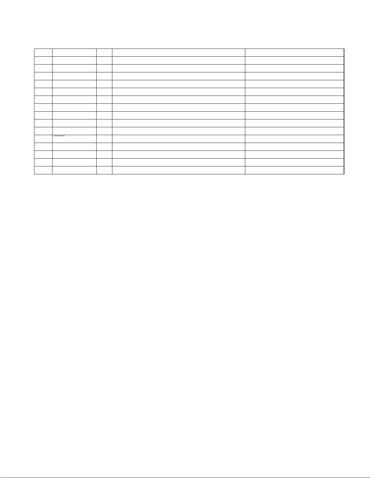
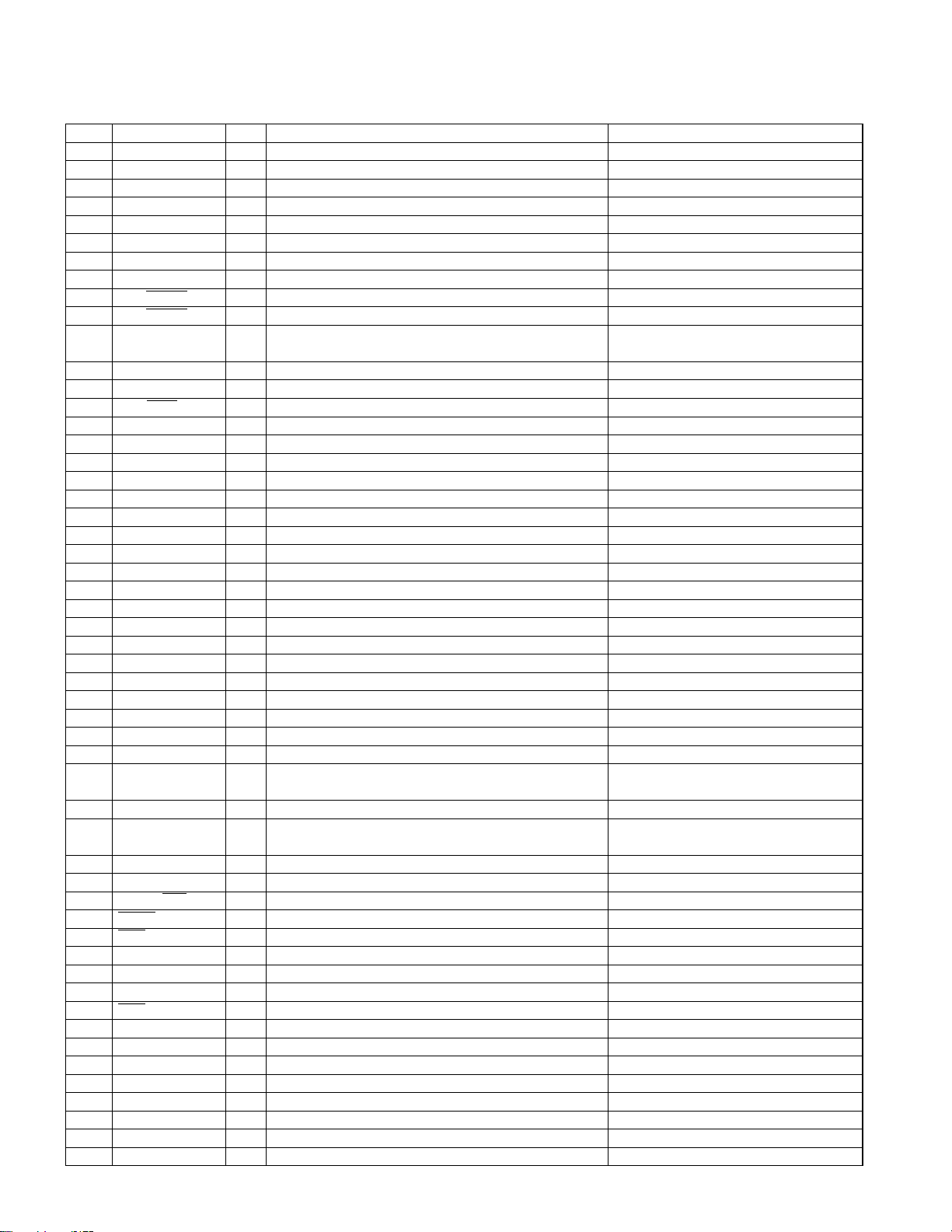
MICROCOMPUTER'S TERMINAL DESCRIPTION
IC2 (CD PLAYER UNIT)
•
PIN No.
1
2
3
4,5
6
7
8
9
10
11
12
13
14
15
16
17
18
19
20
21
22
23
24
25
26
27
28
29
30
31
32
33
34,35
36
37-39
40
41
42
43
44
45
46
47-71
72
73-80
81
82
83
84
PON
NC
MSTOP
NC
RST
MUTEIN L
MUTEIN R
VDD
X2
X1
VSS
XT2
XT1
RESET
NC
MGSW
EJSW
COMMSW
NC
CH-CON
BUDET
AVDD
AVREF0
HOT
LPS
LOESW
NC
TOFF
SRVSEL
SLNSA
ADJSEL
AVSS
NC
AVREF1
NC
DATAH
DATAC
HCLK
REQC
CHMUTE
MUTE L
MUTE R
NC
VSS
NC
VDD
NC
REQH
SP/LO+
I/OPin Name Description Processing Operation
O
PON output
-
O
Mechanism stop signal
-
O
Mechanism
I
Lch MUTE signal input
I
Rch MUTE signal input
-
Positive power supply voltage connection terminal
-
Oscillator connection terminal 2
I
Oscillator connection terminal 1
Ground connection terminal
Sub clock resonator connection terminal 2
Sub clock resonator connection terminal 1
I
Reset input
I
Magazine switch
I
Eject switch
I
Communication Old/New switch input
I
Changer control input from H/U
I
Momentary power down detection
-
A/D converter analog power supply terminal
I
A/D converter reference voltage input
I
Rise in temperature detection
I
Mechanical deck position detection
I
Loading complete switch
I
Tracking off mode
I
Servo active mode
I
Sled non-sensitive area ON/OFF
I
Servo automatic adjustment ON/OFF
-
A/D converter reference ground terminal
-
-
A/D converter reference voltage
I
Data input from H/U
O
Data output from the changer
I/O
Communication clock with H/U
O
Communication request to H/U
O
Audio mute output to H/U
O
Lch audio mute output
O
Rch audio mute output
-
-
Ground connection terminal
-
-
Positive power supply connection terminal
I
Communication request from H/U
O
Spindle/Loading control terminal
µ
-com reset signal
H: Power OFF L: Power ON
L: Mechanism stop
L: Reset
L: Mute ON
L: Mute ON
H: Magazine in
H: Switch ON
H: New L: Old
H: System ON
H:
Momentary power down detection ON
4V(90°C) or greater : detection
4V or less : Not detection
L: Loading complete
H: Tracking OFF
H: Servo mode
L: Non-sensitive ON
H:Automatic adjustment OFF
L: Mute ON
L: Mute ON
L: Mute ON
6
KDC-CX89/CMP59FM/C719MP/CPS89MP
MICROCOMPUTER'S TERMINAL DESCRIPTION
PIN No.
85
86
87
88,89
90
91
92
93
94
95
96
97
98
99
100
SP/LOELV+
ELVNC
TEST1
TEST2
8V/7V
EEPWR
TEST/VPP
DATA
CLK
SDA
SCL
NC
ARMSW
I/OPin Name Description Processing Operation
O
Spindle/Loading control terminal
O
Mechanism deck ascent/descent terminal
O
Mechanism deck ascent/descent terminal
I
TEST mode terminal
I
TEST mode terminal
O
Mechanism movement driver IC power supply voltage control
I
EEPROM Write mode
I
Flash ROM program mode
I/O
Mechanism
I/O
Mechanism µ-com communication serial clock input/output
I/O
DATA input/output with EEPROM
O
Clock output to EEPROM
I
Arm switch
µ
-com communication serial data input/output
H : Write L : normal
H : Arm switch ON
7
KDC-CMP59FM
MICROCOMPUTER'S TERMINAL DESCRIPTION
IC2 (RF MODULATOR UNIT) For KDC-CMP59FM
•
8
PIN No.
1
2
3,4
5
6
7-9
10
11
12
13
14
15
16
17
18
19
20
21
22
23-25
26
27,28
29
30
31
32
33-35
36
37
38
39
40-58
59
60
61
62
63
64,65
66
67
68
69
70
71
72
73
74
75
76
77
78
79
80
XIN
TEST2
PG3,PG2
PG1
PG0
PH3-PH1
PH0 MUTE1
PF3 MUTE0
PF2 REQC
PF1 REQH
PF0 CHCON
PE3 DATA IN
PE2 DATA OUT
PE1 SCK
PE0
PD3 DATA OUT
PD2 CLK
PD1 RST
PD0 CE
PC3-PC1
PC0 SEPA
PB3,PB2
PB1 GAIN1
PB0 GAIN2
VDD+5V
PA3 DATA IN
PA2-PA0
PI31 S28
PI21 S27
PI11 S26
PI01 S25
S24-S6
ALC LOW S5
MUTE S4
SEP A TT S3
RELAY S2
P ON S1
COM2,COM1
REMO INT
HOLD
RES
AOI
HCTR
LCTR
SNS
VDD
FMIN
AMIN
VSS
EO1
EO2
TEST1
XOUT
I/OPin Name Description Processing Operation
I
Main clock resonator connection terminal
I
Test mode terminal 2 for test mode
I
I
I
O
O
O
I
Communication request input from CH
O
Communication request output to CH
O
Control output to CH
I
Data input from CH
O
Data output to CH
O
Clock output to CH
O
Data output to LCD
O
Clock output to LCD
O
Reset output to LCD
O
CE output to LCD
O
Separation select output
O
O
O
GAIN1 output
O
GAIN2 output
-
Positive power supply connection terminal
I
Data input from LCD
I
O
O
O
O
O
O
Mute output
O
Separation attenuator output
O
Relay SW control
O
P ON output
O
O
Remote control sensor input
I
Hold input
I
I
I
I
I
I
Positive power supply connection terminal
FM input
I
AM input
I
Ground connection terminal
FM frequency control output
O
O
Test mode terminal 1 for test mode
I
Main clock resonator connection terminal
-
Not used (pull down to GND lines.)
Not used (pull down to GND lines.)
Not used (pull up to +5V lines.)
Not used (pull down to GND lines.)
Not used (N.C.)
Not used (N.C.)
Not used (N.C.)
"Lo" : Communication requested
"Lo" : Communication requested
"Hi" : Operation mode,
"Lo" : Standby mode
Not used (N.C.)
"Lo" : Reset
Not used (N.C.)
"Hi" : Mode1, "Lo" : Mode2
Not used (N.C.)
"Hi" : Level 1/3, "Lo" : Level 2/4
"Hi" : Level 3/4, "Lo" : Level 1/2
Connected to +5V lines.
Not used (connected to GND lines.)
Not used (N.C.)
Not used (N.C.)
Not used (N.C.)
Not used (N.C.)
Not used (N.C.)
Not used (N.C.)
"Hi" : POWER OFF mode
"Lo" : POWER ON mode
"Hi" : Mode2, "Lo" : Mode1
"Hi" : RF modular output,
"Lo" : Vehicle antenna output
"Hi" : RF modulator circuit is active.
Not used (N.C.)
"Lo" : Microprocessor stop
Not used (pull up to +5V lines.)
Not used (pull down to GND lines.)
Not used (pull down to GND lines.)
Not used (pull down to GND lines.)
Not used (pull down to GND lines.)
Connected to +5V lines.
Not used (pull down to GND lines.)
Connected to GND lines.
Not used (N.C.)
Not used (pull down to GND lines.)
KDC-CX89/CMP59FM/C719MP/CPS89MP
ADJUSTMENT
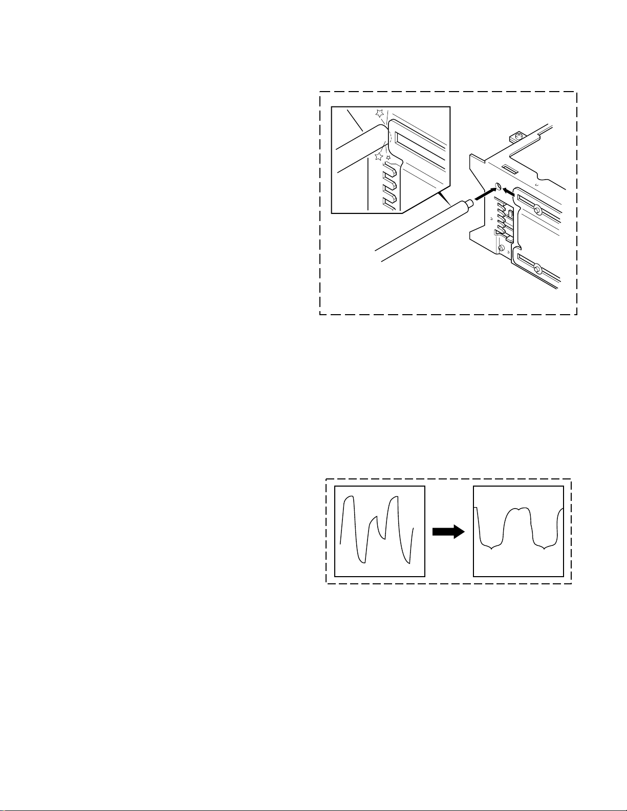
L.P.S initial position adjustment procedure
1. Connect the changer to the H/U.
2. While holding the magazine eject button of the changer,
press the reset button of the H/U.
3. After about 3 seconds, release the magazine eject button.
4. Press the SRC button of the H/U to enter the CD-CH mode,
and the H/U's display section indicates "E-88".
5. Move the mechanism deck to around the 1st stage by
pressing the DISC- or DISC+ button.
6. Insert the adjustment tool (W02-0635-00) into the tool hole
on the changer mechanism.
7. Then press the DISC+ button to move the mechanism deck
until the mechanism's slider hits the adjustment tool.
8. When the motor locks (stops), press the REPEAT key of
the H/U.
When the REPEAT key is pressed, the mechanism moves
automatically to the 1st stage and the initial position
adjustment completes. (The data is written in the EEPROM
at this time.)
W05-0635-00
For KDC-CMP59FM
RF MODULATOR UNIT
1. DC balance adjustment (VR301)
While observing the waveform with an oscilloscope at pin
13 of IC301, adjust VR301 to minimize the waveform level.
2. PLL control voltage adjustment (VC301)
First set the transmission frequency to ∗87.9MHz with the
commander, then adjust VC301 so that the DC Voltage at
the +pole of C317, measured using a multi-meter or digital
tester, is +3V (±0.1V).
∗NOTE: E type is 87.7MHz.
3. Modulation level adjustment (VR303)
The method uses a standard receiver or tuner.
Adjust VR303 so that the output level from the standard
receiver or tuner is as specified.
9
 Loading...