

KENWOOD KDC-CPS85 Service Manual
CD AUTO CHANGER
KDC-CX85/CPS85
SERVICE MANUAL
© 1999-11 PRINTED IN JAPAN
B51-7552-00 (N) 3444
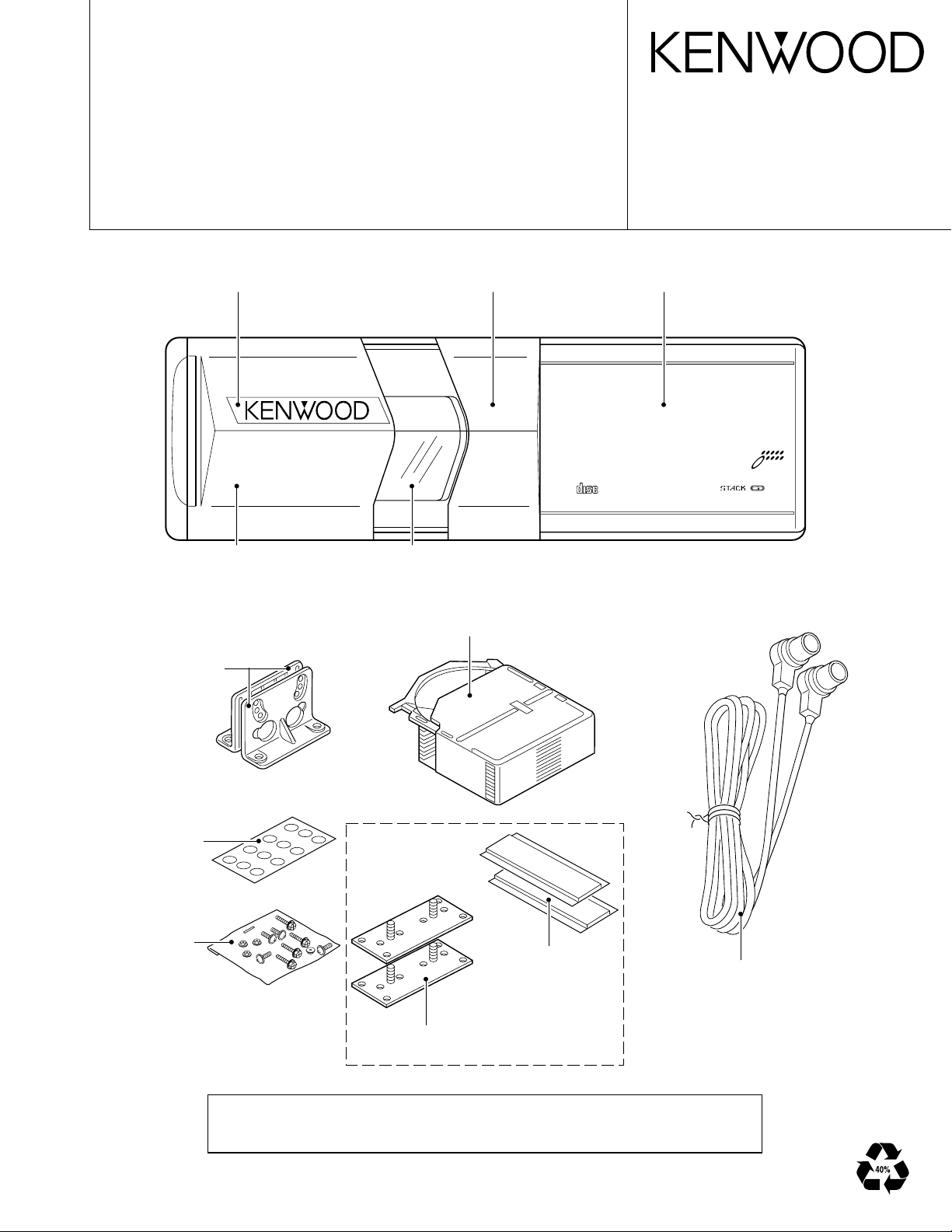
BADGE
CX85 :(B43-1238-04)
CPS85:(B43-1237-04)
BRACKET
(J19-4712-13)
DRESSING PANEL
CX85 :(A21-3535-12)
CPS85:(A21-3544-12)
DRESSING PANEL
CX85 :(A21-3538-12)
CPS85:(A21-3545-12)
FRONT GLASS
CX85 :(B10-3076-04)
CPS85:(B10-2997-04)
HOLDER ASSY(MAGAZINE)
(J19-4676-52)
PANEL
CX85 :(A64-1991-01)
CPS85:(A64-1993-01)
DISC
COMPACT DISC AUTO CHANGER KDC-CPS85
NEW ANTI VIBRATION MECHANISM
COMPACT
D.R.I.V.E.
DIGITAL AUDIO
DYNAMIC RESOLUTION INTENSIVE VECTOR ENHANCEMENT
10
DISC NAME PRESET
TEXT
BLIND PLATE
(F19-1303-04)
SCREW SET
K/E TYPE:
(N99-1645-15)
M TYPE:
(N99-1628-15)
ADHESSIVE T APE
(J69-0506-04)
MOUNTING HARDWARE ASSY
(J21-7775-04)
M TYPE ONL Y
CORD WITH PLUG
(E30-4138-05)
The MECHANISM OPERATION is the same as model KDC-C710.
Please refer to the service manual of model KDC-C710(B51-7104-00).
KDC-CX85/CPS85
M5V
XOFF
LIM SW
L.P.S.
EJ SW
ARM SW
12.5MHz
AVREF0
X2
SPINDLE
SLED
M
M
LOE SW
FO. COIL
TR. COIL
B
A
UPC63702A
BTL DRIVER
ELEVATOR
EEPROM
AK93C45AF
HOT
UPC2572A
APC
A5V
Q22
+B
BA6791FP
UPD784214GC066
SYSTEM u-COM
IC7
IC9
SIGNAL
PROCESSOR
IC13
RF AMP
16.9344MHz
X1
P ON
Q6
VOLTAGE SELECT
Q999
AVR
Q998
5V AVR
IC10
IC11
5
10
14
4
3
8
2
4
IC12
BA6219FP-Y
LC89170M
TEXT
DECODER
IC8
4
4
MG SW
Q21
SERVO+B
+B
COMM SW
IC5
LC3564ST
S-RAM
24
DSP5V
M5V
MOTOR DRIVE
C
D
IC6
DAC
DIGITAL FILTER
D.R.I.V.E.
4
KKZ05F
L.P.F
NJM5532MD
IC1
Q1,2
MUTE
X1
4.19MHz
AUX SW
UPD78058GC82T
I/F u-COM
IC1
IC2
RST
+5V
6
Q7
BU
BU14V
CH MUTE
CH RST
REQC0
CHCON
DATAH0
DATAC0
REQH0
HCLK0
AUDIO
OUT
BU14V
CH RST2
CH MUTE2
HCLK2
REQC2
DATAC2
REQH2
CHCONO2
DATAH2
6
AUDIO
AUX to AUX
CH2
H/U
8
RELAY
K1,3
K2,4
RELAY
DET
to
to
AUDIO VREF
IC2
5VREG
IC3
DA5V
+B
M
PICKUP ASSY
(X13-9730-00)
(X32-4680-00)
(X13-9790-00)
(X92-3630-02)
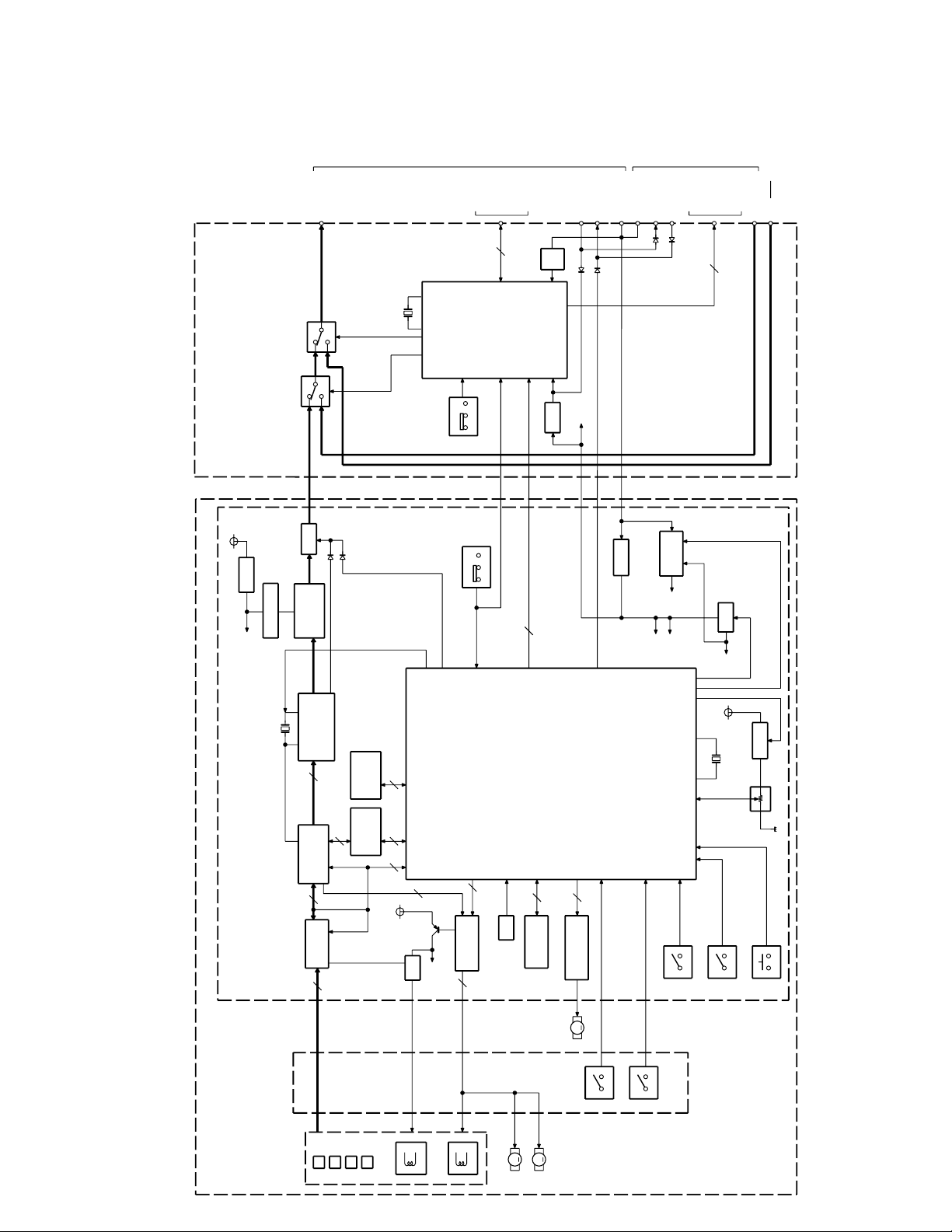
BLOCK DIAGRAM
2
KDC-CX85/CPS85
MICROCOMPUTER’S TERMINAL DESCRIPTION
UPD 7805GCB82T : IC1 (X13-9790-00)
Pin Pin Name I/O Function Description
1 P15/AN15 O Not used.
2 P16/AN16 O Not used.
3 P17/AN17 O Not used.
4 AVss - A/D converter reference ground terminal
5 P130/ANO0 O RSTOUT Reset output H: Reset
6 P131/ANO1 O REQH1 Communication request output to CH1 L: Request
7 AVref1 I AVref1 A/D converter reference power terminal
8 P70/SI2/RXD I DATAC1 Data input from CH1
9 P71/SO2/TXD O DATAH1 Data output to CH1
10
P72/SCK2/ASCK
11 P20/SI1 I DATAH0 Data input from H/U
12 P21/SO1 O DATAC0 Data output to H/U
13 P22/SCK1 I/O HCLK0 Communication clock input/output to/from H/U
14 P23/STB O REQC0 Communication request output to H/U
15 P24/BUSY O REQH2 Communication request output to CH2
16
P25/SI0/SB0/SDA0
17
P26/SO0/SB1/SDA1
18 P27/SCK0/SCL I/O HCLK2 Communication clock input/output to/from CH2
19 P40/AD0 O CHCONO1 Control output to CH1 H: CH1 control output
20 P41/AD1 O CHCONO2 Control output to CH2 H: CH2 control output
21 P42/AD2 O RELAY1 Control output to RELAY1 H: AUX L: CH1
22 P43/AD3 O RELAY2 Control output to RELAY2 H: CH2 L: CH1
23 P44/AD4 O MSTOP BU instant dip detection output to CH1
24 P45/AD5 O Not used.
25 P46/AD6 O Not used.
26 P47/AD7 O Not used.
27 P50/A8 O Not used.
28 P51/A9 O Not used.
29 P52/A10 O Not used.
30 P53/A11 O Not used.
31 P54/A12 O Not used.
32 P55/A13 O Not used.
33 VSS - VSS Connected to GND.
34 P56/A14 O Not used.
35 P57/A15 O Not used.
36 P60 O Not used.
37 P61 O Not used.
38 P62 O Not used.
39 P63 O Not used.
40 P64 O Not used.
I/O HCLK1 Communication clock input/output to/from CH1
I DATAC2 Data input from CH2
O DATAH2 Data output to CH2
Processing Operation
L: Communication request
L: Communication request
H: BU instant dip
detection output
3

KDC-CX85/CPS85
MICROCOMPUTER’S TERMINAL DESCRIPTION
Pin Pin Name I/O Function Description
41 P65 O Not used.
42 P66 O Not used.
43 P67 O Not used.
44 P30 O Not used.
45 P31 O Not used.
46 P32 O Not used.
47 P33 O Not used.
48 P34 O Not used.
49 P35 O Not used.
50 P36 O Not used.
51 P37 O Not used.
52 P120/RTP0 O Not used.
53 P121/RTP1 O Not used.
54 P122/RTP2 O Not used.
55 P123/RTP3 O Not used.
56 P124/RTP4 O Not used.
57 P125/RTP5 O Not used.
58 P126/RTP6 O Not used.
59 P127/RTP7 O Not used.
60 RESET I RESET RESET L:RESET
61
P00/INTP0/TI00
62
P01/INTP1/TI01
63 P02/INTP2 I AUX SW External input switch H: External input
64 P03/INTP3 I REQH0 Communication request input form H/U
65 P04/INTP4 I REQC1 Communication request input from CH1
66 P05/INTP5 I CHCON1 CH1 control input from H/U L: Control on CH1
67 P06/INTP6 I COMMSW 5-line communication old/new selection swtcih
68 Vdd - VDD Positive power voltage
69 X2 - X2 Oscillator connection terminal
70 X1 I X1 Oscillator connection terminal
71 IC(Vpp) - IC Internal connection terminal
72 XT2 - XT2
73 XT1/P07 I CHCON2 CH2 control input from H/U L: Control on CH2
74 Avdd - AVDD A/D analog power voltage
75 AVref0 I AVREF0 A/D reference voltage input
76 P10/ANI0 O Not used.
77 P11/ANI1 O Not used.
78 P12/ANI2 O Not used.
79 P13/ANI3 O Not used.
80 P14/ANI4 O Not used.
I REQC2 Communication request inpout from CH2
I BUDET BU instant dip detection input
Processing Operation
L: Communication request
H: BU instant dip detection
L: Communication request
L: Communication request
H: New communicaton
L: Old communication
4
KDC-CX85/CPS85
MICROCOMPUTER’S TERMINAL DESCRIPTION
●UPD 784214GC-066 : IC7 (X32-4680-00)
Pin Pin Name I/O Function Description
1 P120/RTP0 O LDON Pickup laser ON H: Laser ON
2 P121/RTP1 O TBCO Tracking filter coefficient switching signal output H: Gain-up mode
3 P122/RTP2 I TBCI Tracking filter coefficient switching signal input H: Gain-up mode
4 P123/RTP3 I RFOK Focus ON status signal input H: Focus ON
5 P124/RTP4 O XOFF Servo IC oscillation stop control
6 P125/RTP5 O RST Servo IC reset terminal L: Reset
7 P126/RTP6 O SAO Servo IC address setting
8 P127/RTP7 O SSTB Servo IC communication strobe
9 VDD - VDD Positive power voltage connection terminal
10 X2 - X2 Oscillator connection terminal 2
11 X1 I X1 Oscillator connection terminal 1
12 VSS VSS GND potential connection
13 XT2 XT2 Subclock connection terminal 2
14 XT1 XT1 Subclock connection terminal 1
15 RESET I RESET Reset
16 P00/INTP1 I SBSY Sub-code Q read timing detection terminal
17 P01/INTP2 I MGSW Magazine switch H: Magazine in
18 P02/INTP2 I EJSW Eject switch H: Swtich ON
19 P03/INTP3 I COMMSW 5-line communicatin old/new swtich
20 P04/INTP4 I DQSY Text data read permission signal input
21 P05/INTP5 I CHCON Changer control input from H/U
22 P06/INTP6 I BUDET BU instant dip detection terminal
23 AVDD - AVDD A/D converter analog power terminal
24 AVREF0 I AVREF0 AD converter reference voltage input
25 P10/ANI0 I HOT Rise in temperature detection
26 P11/ANI1 I LPS Mechanical deck position detection
27 P12/ANI2 I LOESW Loading compete switch
28 P13/ANI3 I LIMSW Limit switch
29 P14/ANI4 I TYPE0 For test mode
30 P15/ANI5 I TYPE1 For test mode
31 P16/ANI6 I SLG1 For setting thread loop gain
32 P17/ANI7 I SLG2 For setting thread loop gain
33 AVSS - AVSS A/D converter reference GND terminal
34 P130/ANO0 O LPSCO A/D converter reference power control
35 P131/ANO1 O AMUTE Audio mute L: Mute ON
36 AVREF1 - AVREF1 A/D converter reference power terminal
37
P70/RxD2/SO2
38
P71/TxD2/SO2
39
P72/ASCK2/SCK2
40 P20/RxD1/SI1 I DATAH Data input from H/U
I SDI Servo IC communication serial data input
O SDO Servo IC communication serial data output
O SCK Servo IC communication serial clock output
Processing Operation
H: Oscillatin stop
H: New communication
L: Old communication
L: Loading complete
L: Pickup detection of
innermost track
5
KDC-CX85/CPS85
MICROCOMPUTER’S TERMINAL DESCRIPTION
Pin Pin Name I/O Function Description
41 P21/TxD1/SO1 O DATAC Data output from the changer
42
P22/ASCK1/SCK1
43 P23/PCL O REQC Communication request to H/U
44 P24/BUZ O CHMUTE Audio mute output to H/U L: Mute ON
45 P25/SI0/SDA0 I TXTDATA Text data input
46 P26/SO0 O Not used.
47
P27/SCK0/SCL0
48 P80/A0 O A0 Address setting terminal for S-RAM
49 P81/A1 O A1 Address setting terminal for S-RAM
50 P82/A2 O A2 Address setting terminal for S-RAM
51 P83/A3 O A3 Address setting terminal for S-RAM
52 P84/A4 O A4 Address setting terminal for S-RAM
53 P85/A5 O A5 Address setting terminal for S-RAM
54 P86/A6 O A6 Address setting terminal for S-RAM
55 P87/A7 O A7 Address setting terminal for S-RAM
56 P40/AD0 I/O D0 Data input/output terminal with S-RAM
57 P41/AD1 I/O D1 Data input/output terminal with S-RAM
58 P42/AD2 I/O D2 Data input/output terminal with S-RAM
59 P43/AD3 I/O D3 Data input/output terminal with S-RAM
60 P44/AD4 I/O D4 Data input/output terminal with S-RAM
61 P45/AD5 I/O D5 Data input/output terminal with S-RAM
62 P46/AD6 I/O D6 Data input/output terminal with S-RAM
63 P47/AD7 I/O D7 Data input/output terminal with S-RAM
64 P50/A8 O A8 Address setting terminal for S-RAM
65 P51/A9 O A9 Address setting terminal for S-RAM
66 P52/A10 O A10 Address setting terminal for S-RAM
67 P53/A11 O A11 Address setting terminal for S-RAM
68 P54/A12 O A12 Address setting terminal for S-RAM
69 P55/A13 O A13 Address setting terminal for S-RAM
70 P56/A14 O A14 Address setting terminal for S-RAM
71 P57/A15 O A15 Address setting terminal for S-RAM
72 VSS - VSS Ground potential connection terminal
73 P60/A16 O A16 Enable control terminal for S-RAM
74 P61/A17 O A17 Enable control terminal for S-RAM
75 P62/A18 O RAMOK RAM check judging terminal for production
76 P63/A19 I ELVADJ
77 P64/RD O RD Read-out to S-RAM control output
78 P65/WR O WR Write to S-RAM control output
79 P66/WAIT I WAIT Insertion of weight when accessing S-RAM
80 P67/ASTB O ASTB Chip selection to S-RAM
I/O HCLK Communication clock input from H/U
O TXTCLK Text clock output
Mechanism deck ascent/descent position
adjustment mode
Processing Operation
L: Adjustment mode
6
 Loading...