

Kenwood KD-CCMP-21-V Service Manual
CD AUTO CHANGER PLAYER
KDC-CMP2 1V
SERVICE MANUAL
© 2004-3 PRINTED IN JAPAN
B53-0163-00 (N) 428
The MECHANISM OPERATION is the same as model KDC-C660.
Please refer to the service manual of model KDC-C660 (B51-7105-00).
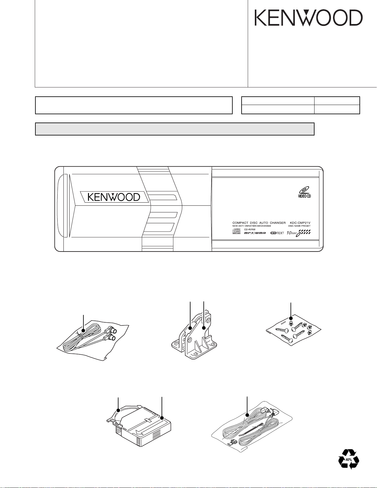
When transporting this model, always attach CAUTION CARD and STEPPED SCREW (for transportation).
Service jig
For initial position setting
Parts No.
W05-0635-00
Cord with plug
(E30-4291-05)
(E30-4711-05)
(E30-6358-05)
Tray
(J99-0614-01)
Bracket (L)
(J19-5018-03)
Holder assy
(J19-5146-02)
Bracket (R)
(J19-5019-03)
Screw set
(N99-1645-15)
Cord with pinjack
(E30-6351-05)
2
BU14V
5V AVR BU5V
BU3.3V
BU2.5V
SW
5V AVR
D5V (SW)
8V AVR
SW
5V REG (A)
SRV8V
BU
DETECT
A5V
NJM2880U33 SW3.3V
TR
SW5V
UPC2926T SW2.6V
SHIFT
LEVEL
CONTROL IC
MICROPROCESSOR
AUDIO DAC HD74LV157AT-EAUDIO MUTE
LIM SW
LIM SW
SW
RESET
EEP-ROM
L.P.S
ARM SW
EJ SW
MG SW
N/PAL SW
SERVO,DSP
DECODER
MP3/WMA
VCD
DECODER
VIDEO AMP
DRAM
FLASH ROM
DC MOTOR
DRIVER
BTL
TR COIL
SLED
FO COIL
ELEVATOR
LO-EJ
SPINDLE/
CB
A
E
F
PD
HOT
IC4 IC15
CQ RF,
MECHANISM
AUDIO
OUT
VIDEO
OUT
IC5
IC8
IC9
IC7
IC11
IC12 IC15
SYSTEM
IC1
IC2
Q90,91 IC14
NJM2890
M1
M2
M3
CHCLK
REQH
REQC
DATAH
DATAC
CHCON
CHRST
CHMUTE
N/PAL
PON
PON
PON
D5V (SW)
16MHz
PON
BU3.3V
BU5V
A5V
A or B
PON
PON
BU3.3V
DATA SEL
12.5MHz
BU5V
GND
16.934MHz
SW3.3V
BU3.3V BU2.5V
AB
SW5V
SW2.6V
75 470u
SW5V
27MHz
XTAL
SRV8V
10
C16M
BCLK,DATA,LRCK
CD PLAYER UNIT (X32-5650-00)
(X13- )
PICKUP ASSY
MECHANISM ASSY (X92-4950-00)
DPU1
KDC-CMP2 1V
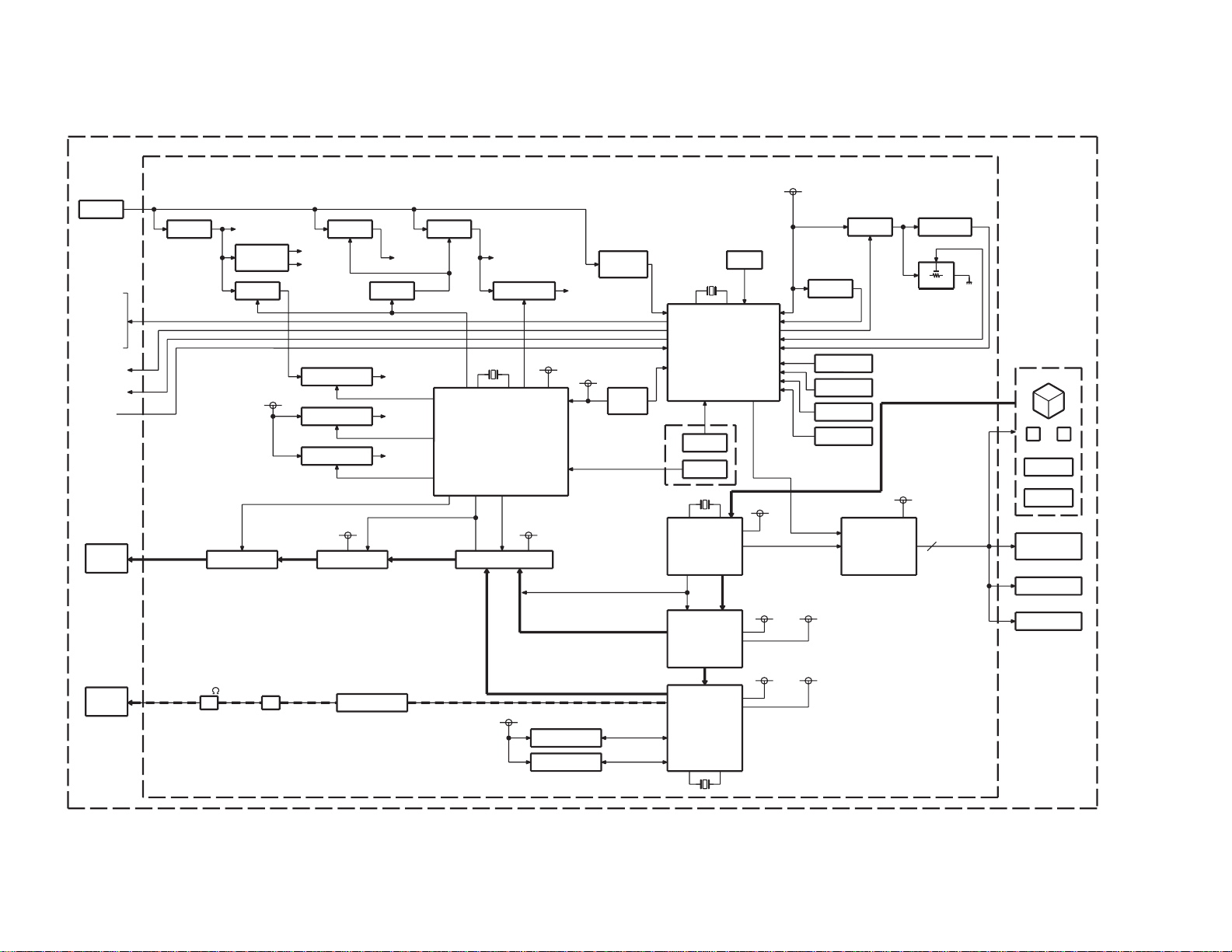
BLOCK DIAGRAM

KDC-CMP2 1V
COMPONENTS DESCRIPTION
● CD PLAYER UNIT (X32-5650-00)
Ref. No. Application / Function Operation / Condition / Compatibility
IC1 Reset IC System microprocessor reset control IC
IC2 System microprocessor Communication to head unit and control for mechanism control IC
IC3 EEPROM LPS data backup memory (for MD position)
IC4 Mechanism control IC Control for Mechanism assy, servo IC and MP3/WMA decoder
IC5 Video amp Video amp for composite video signal
IC6 AVR 2.6V (for IC7 VCC)
IC7 Video decoder Video CD decoder IC
IC8 DRAM For playback video data
IC9 Flash ROM Program memory for VCD decode
IC10 Selector Select for VCD line or MP3/WMA data line
IC11 Decoder MP3/WMA decoder IC
IC12 CD servo IC RF amplifier built in digital servo and data processor IC
IC13 AVR 5.0V (for audio and IC14 VDD)
IC14 Audio DAC Audio DA converter
IC15 Motor driver Focusing coil, tracking coil, spindle motor and sled motor driver
IC16 AVR 5.0V (for IC7 VDD)
IC17 AVR 3.3V, 2.5V (for BU), IC4, IC11 VDD
IC18 AVR 3.3v (for IC12 VDD)
Q1,2 SW AVR 8V control SW
Q3,6 SW AVR 6.2V control SW
Q5 Driver AVR 5V driver
Q7 SW Select for 8V and 7V voltage
Q8 Driver AVR 6.2V driver
Q11 Driver AVR 8V driver
Q12 BU det Backup line voltage detector
Q20 Parking det Parking SW detector
Q21 Reset SW Reset control SW (for system microprocessor)
Q22 SW Changer muting control
Q23 SW Changer control SW
Q24 SW AVR 5V control SW
Q25,26 Level shift Voltage level shift (5.0V →3.3V, 3.3V→5.0V)
Q27,28 Audio muting SW Q27 (for Lch), Q28 (for Rch)
Q40 SW System reset for IC4
Q52 SW System reset for IC7
Q70 Selector SW Selector IC control SW
Q71 VC SW Control for Q73
Q72 LD SW Control for APC
Q73 VC SW Eccentric disc SW (for sub beam F)
Q90~93 Audio muting SW Q90,93 (Rch), Q91,92 (Lch)
Q100 Vref selector Select for internal Verf or external Vref
3

KDC-CMP2 1V
MICROCOMPUTER’S TERMINAL DESCRIPTION
● SYSTEM MICROPROCESSOR : 784214AGC-204 (X32: IC2)
Pin No. Pin Name I/O Description / Processing Operation
1 PON O Power control output terminal (L : AVR power ON)
2NCONC (open)
3/MSTOP O Mechanism stop signal output terminal (L : Mechanism stop, H : NORMAL)
4PARK SW I Parking SW detect input terminal (H : Monitor ON, L : Monitor OFF)
5 NTSC/PAL I NTSC/PAL select terminal (H : PAL, L : NTSC)
6 RST O Servo IC reset signal output terminal (L : Reset)
7 /MUTEIN L I Lch muting signal input terminal (L : Muting ON)
8 /MUTEIN R I Rch muting signal input terminal (L : Muting ON)
9 VDD - BU5V (for ADC)
10 X2 - X’tal 12.5MHz
11 X1 - X’tal 12.5MHz
12 VSS - GND
13,14 XT2,XT1 - NC
15 /RESET I Reset signal input terminal (L : Reset)
16 NC - NC
17 MGSW I Magazine in SW input terminal (H : Magazine pack in)
18 EJSW I Eject SW input terminal (H : Eject SW ON)
19 COMMSW I Select for OLD or NEW 5L line system control
20 NC - NC
21 CH-CON I Changer control for Head unit (H : System ON)
22 BUDET I Backup line voltage detect input terminal (H : Momentary power down)
23 AVDD - VDD for A/D converter (BU5V)
24 AVREF0 I Vref for A/D converter (Sys 5V)
25 HOT I Rise in temperature detect input terminal (Detect level : 4V (90°C))
26 LPS I Mechanical deck position detect input terminal
27 LOESW I Loading in SW input terminal (L : Loading complete)
28 NC - NC
29 TOFF I Tracking OFF mode detect terminal (H : Tracking OFF)
30 SRVSEL I Servo active mode terminal (No mechanism movement, H : Servo active mode)
31 SLNSA I SLED non-sensitive area ON/OFF terminal (L : Seld non-sensitive ON)
32 ADJSEL I Servo automatic adjustment ON/OFF terminal (L : Servo adjustment ON)
33 AVSS - GND
34,35 NC - NC
36 AVREF1 I Vref for A/D converter (BU 5V)
37~39 NC - NC
40 DATAH I Data input terminal (for Head unit)
41 DATAC O Data output terminal (for Changer unit)
42 HCLK I/O Communication clock (for Head unit)
43 REQC O Communication request to Head unit
44 CHMUTE O Audio muting signal to Head unit (L : Muting ON)
45 /MUTE L O Lch audio muting signal output terminal (L : Muting ON)
4
KDC-CMP2 1V
MICROCOMPUTER’S TERMINAL DESCRIPTION
Pin No. Pin Name I/O Description / Processing Operation
46 /MUTE R O Rch audio muting signal output terminal (L : Muting ON)
47~71 NC - NC
72 VSS - VSS
73~75 NC - NC
76 ELVADJ I Mechanism deck position adjustment mode select terminal (L : Adjustment mode)
77~80 NC - NC
81 VDD - VDD (BU 5V)
82 NC - NC
83 REQH Communication request from Head unit
84 SP/LO+ O Spindle/Loading motor control terminal
85 SP/LO- O Spindle/Loading motor control terminal
86 ELV+ O Elevator motor control terminal
87 ELV- O Elevator motor control terminal
88,89 NC - NC
90,91 TEST1,TEST2 I Test mode terminal
92 8V/7V O Mechanism driver IC control terminal
93 EEPWR I EEPROM writing mode control terminal (H : Writing, L : NORMAL)
94 TEST/VPP I Flash ROM program mode control terminal
95 DATA I/O Serial data communication to mechanism control IC
96 /CLK I/O Serial clock communication to mechanism control IC
97 SDA I/O EEPROM data I/O terminal
98 SCL O EEPROM clock output terminal
99 NC - NC
100 ARMSW I ARM SW detector (H : Arm SW ON)
● MECHANISM CONTROL IC : 91CW12AFG-5DN4 (X32 : IC4)
Pin No. Pin Name I/O Description / Processing Operation
1 VREFL I Reference V input terminal (for ADC)
2AVSS - GND (for ADC)
3AVCC - BU3.3V (for ADC)
4NCONC (open)
5 20RST O Reset control terminal (for decoder, L : RESET, H : NORMAL)
6 20ACK I Acknowledge signal input terminal (for decoder)
7 20STBY O Stand-by control terminal (for decoder, H : STAND BY, L : NORMAL)
8,9 NC O NC (open)
10 20INT I Interrupt signal input terminal (for decoder)
11 FOGUP I Focus gain interrupt input terminal (H : Fo gain UP, L : NORMAL)
12 LZM I 0bit MUTE detect (Lch) (L : MUTE OFF, H : MUTE ON)
13 RZM I 0bit MUTE detect (Rch) (L : MUTE OFF, H : MUTE ON)
14,15 NC O NC
16 20CS O Chip select signal output terminal (for decoder)
17 20LP O Latch pules signal output terminal (for decoder)
5
KDC-CMP2 1V
MICROCOMPUTER’S TERMINAL DESCRIPTION
Pin No. Pin Name I/O Description / Processing Operation
18 20TXD0 I/O Serial data signal output terminal (for decoder)
19 20RXD0 I Serial data signal input terminal (for decoder)
20 20SCLK0 O Serial data clock output terminal (for decoder)
21 DSPTXD1 O Serial data signal output terminal (for DSP)
22 DSPRXD1 I Serial data signal input terminal (for DSP)
23 DSPSCLK1 O Serial data clock output terminal (for DSP)
24 AM0 I Select for ROM mode (H : NORMAL, L : External ROM mode)
25 DVCC - BU3.3V
26 X2 O X’tal 16MHz
27 DVSS - GND
28 X1 I X’tal 16MHz
29 AM1 I Fixed H
30 RESET I Reset input terminal (L : RESET, H : NORMAL)
31~34 NC O NC
35 DSPSTB O Data strobe signal output terminal (for DSP)
36 DSPA0 O Command, parameter select signal (for DSP) (H : Parameter, L : Command)
37 DSPRST O Reset control output terminal (for DSP)
38 DSPINT I Interrupt signal input terminal (for DSP) (H : Interrupt)
39 /DAC RESET O Reset signal output terminal (for DSP) (L : RESET, H : NORMAL)
40 SEARCH O Search condition output terminal (H : Search, L : NORMAL)
41 LOE/LIM_SW I SLT SW detect input terminal (H : Inside)
42~45 NC O NC
46 PONE5 O +5V power supply control (for video) (H : POWER ON)
47 PONE2.5 O +2.5V power supply control (for video) (H : POWER ON)
48~60 NC O NC
61 /DAC PD O DAC RESET (L : RESET, H : NORMAL)
62 DVSS - GND
63 NMI I Request for non maskable interrupt signal input terminal
64 DVCC - +VCC
65 DAC MUTE O DAC MUTE control terminal (H : MUTE, L : MUTE OFF)
66 DAC PON O Audio power supply (for DXM6550) (H : Power ON)
67 PONA5 O +5V Audio power supply (for DXM6550) (H : Power ON)
68 ESRST O Reset signal output terminal (for ES3890) (L : RESET, H : NORMAL)
69 VMUTE O VIDEO MUTE control terminal (H : MUTE, L : MUTE OFF)
70 NC O NC
71 SELINT O Video/Audio select output terminal (H : NORMAL, L : Interrupt)
72 ASEL0 O Audio signal output select terminal 0 (00 : STEREO, 01 : Lch)
73 ASEL1 O Audio signal output select terminal 0 (10 : Rch, 11 : Not function)
74 NT/PAL O NTSC/PAL selector (L : NTSC, H : PAL)
75 DATASEL O 20F/ES3890 output select (H : 20F, L : ES3890)
76,77 NC O NC
78 NC (BOOT) I Flash memory writing terminal (L : Writing, H : NORMAL)
6
KDC-CMP2 1V
MICROCOMPUTER’S TERMINAL DESCRIPTION
Pin No. Pin Name I/O Description / Processing Operation
79,80 NC O NC
81 POND3.3 O D3.3V POWER ON control terminal (H : POWER ON)
82 MUTEL O Audio muting control terminal (Lch)
83 MUTER O Audio muting control terminal (Rch)
84 SDA I/O I2C data (for system microprocessor)
85 SCL I/O I2C clock(for system microprocessor)
86 MSTOP I Interrupt for stand-by condition (L : STOP, H : NORMAL)
87 NC O NC
88 DMUTE O Driver muting (L : MUTE ON, H : MUTE OFF)
89 DVCC - VDD
90 NC O NC
91 DVSS - GND
92~94 NC I NC
95 VCDSEL I Video CD operation control terminal
96 ASEL I Audio output polarity control terminal (H : Reversal output, L : Normal output)
97 CHSEL I Destination input terminal (H : Changer, L : Normal)
98 SEL0 I Destination input terminal (L,L : DXM-6540, L,H : DXM6550)
99 SEL1 I Destination input terminal (H,H : DXM6560)
100 VREFH I Reference voltage input terminal (for ADC : BU3.3V)
ADJUSTMENT
● L.P.S. initial position adjustment procedure
1. Connect the changer to the HEAD UNIT (H/U).
2. While holding the magazine eject button of the changer,
press the reset button of the H/U.
3. After about 3 seconds, release the magazine eject button.
4. Press the SRC button of the H/U to enter the CD-CH mode,
and the H/U's display section indicates “E-88”.
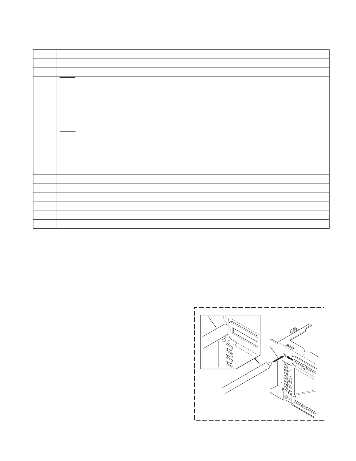
5. Move the mechanism deck to around the 1st stage b y pressing the DISC- or DISC+ button.
6. Insert the adjustment tool (W05-0635-00) into the tool hole
on the changer mechanism.
7. Then press the DISC+ button to move the mechanism dec k
until the mechanism’s slider hits the adjustment tool.
8. When the motor locks (stops), press the REPEAT key of
the H/U.
When the REPEAT key is pressed, the mechanism moves
automatically to the 1st stage and the initial position adjustment completes. (The data is written in the EEPROM at
this time.)
W05-0635-00
7
 Loading...