

Kenwood KDC-2016, KDC-35MR, KDC215S, KDC-2016/215S Service Manual
CD RECEIVER
KDC-2016/215S
Q
Q
3
7
6
3
1
5
1
5
0
KDC-35MR
SERVICE MANUAL
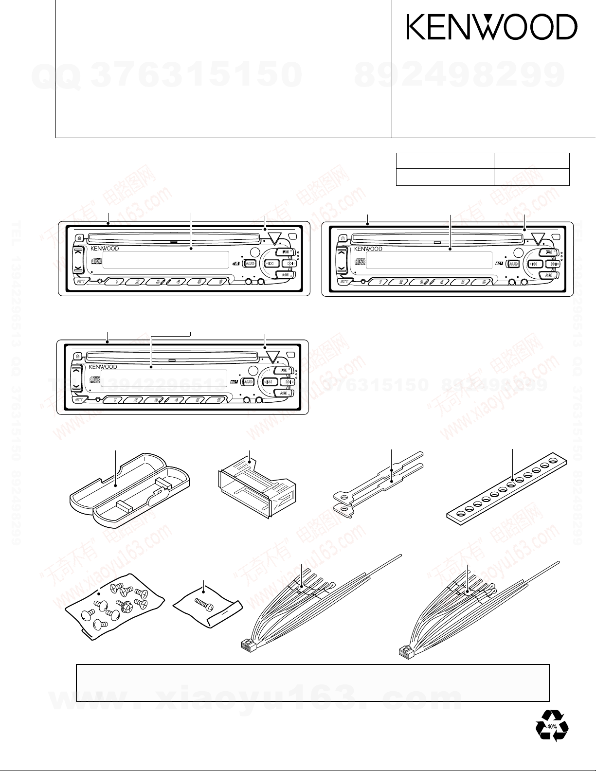
Escutcheon
TEL 13942296513 QQ 376315150 892498299
(B07-2181-02)
Escutcheon
(B07-2169-02)
TEL
KDC-2016
LOUD
KDC-35MR
13942296513
LOUD
Front glass
(B10-3125-01)
SCAN RDM REP
Front glass
(B10-3123-11)
CD MD-CHANGER CONTROL
SCAN RDM REP
Panel assy
(A64-1891-02)
SRC
PWR
OFF
X
45W 4
45W 4
M.RDM
D.SCN
A.ADJ
AUTO
AME ADJ
Panel assy
(A64-1889-02)
X
A.ADJ
AUTO
AME ADJ
CRSC
CLK
SRC
PWR
OFF
CRSC
DISC
DISC
Q
CLK
Q
Escutcheon
(B07-2181-02)
7
3
6
8
LOUD
3
9
1
5
4
2
© 1999-11 PRINTED IN JAPAN
B51-7563-00 (N) 1794
Extension cord
CD mechanism(22P) W05-0618-00
Front glass
(B10-3122-01)
KDC-215S
SCAN RDM REP
0
5
1
9
8
9
2
2
8
Panel assy
(A64-1888-02)
X
45W 4
4
9
A.ADJ
AUTO
AME ADJ
8
9
Parts No.
PWR
OFF
CLK
9
2
SRC
9
9
TEL 13942296513 QQ 376315150 892498299
CRSC
Plastic cabinet assy
(A02-1486-13)
Screw set
(N99-1632-05)
w
w
Mounting hardware assy
(J21-9491-03)
DC cord
y
u
(E30-4783-05)
:KDC-215S/35MR
1
6
Screw set
(N99-1610-15)
:KDC-2016/215S
The MECHANISM OPERATION DESCRIPTION is the same as model KDC-S3007 and KDC-5050RG.
Please refer to the service manual for model KDC-S3007(B51-7029-00) or KDC-5050RG(B51-7099-00).
w
.
xia
o
Lever x2
(D10-3031-04)
3
.
c
o
m
DC cord
(E30-4784-05)
:KDC-2016
Stay
(J54-0606-04)
KDC-2016/215S/35MR
CONTENTS
7
Q
Q
3
TEL 13942296513 QQ 376315150 892498299
6
BLOCK DIAGRAM........................................................................................ 2
COMPONENTS DESCRIPTION ................................................................... 3
TERMINAL DESCRIPTION........................................................................... 5
ADJUSTMENT ............................................................................................. 7
PC BOARD.................................................................................................... 8
SCHEMATIC DIAGRAM ............................................................................. 15
EXPLODED VIEW....................................................................................... 23
PARTS LIST ................................................................................................ 26
SPECIFICATIONS .................................................................... BACK COVER
3
1
5
1
5
0
BLOCK DIAGRAM
IC2
FM
AM
Q
CD
CH
QUAL
LEVEL
A8V
E-VOL
Q
and
MPX
VDD
3
7
TUNER
FM+B
AM+B
IF1/IF2/PLL+B
VDD 5V
AUDIO OUT
TEL
S-METER
Q200,201
FM+B
Q202,203
AM+B
TUN5V
13942296513
SD
382mV
170mV
1200mV
1200mV
8
Q153,154
MUTE
1
3
6
IC5,
Q155,156
MUTE DRIVER
9
5
1
2
5
IC4
4
0
POWER IC
9
8
9
8
2
FM
4
AM
CD
CD-CH
9
2
9
PRE OUT
1605mV
9
2
8
561mV
3529mV
3529mV(KDC-35MR)
SP-OUT
9
TEL 13942296513 QQ 376315150 892498299
9
KDC-35MR
CN
KDC-35MR
w
2
CD
SW1
SW2
SW3
CLK
DATA M
DATA S
SRQ
MUTE
CS
RST
STOP
LO/EJ
MO SW
CH
RST
REQ C
CLK
DATA H
CH-CON
REQ H
DATA C
MUTE
w
SERVO
A8V
BU5V
BACK
UP
w
BU5V
IC3,Q50
RST
(X13)
RST SW
.
xia
QUAL
RDDA
RDCK
PAN 5V
IC1
LCD DRIVER
WITH
KEY MATRIX
DATAS
LCD
CLKCEDATAL
NOISE
AFC
IC2
REMOTE
CONTROL
KDC-35MR
o
IC1
u-COM
SCL
SDA
REMO
PANEL
y
SD
PANEL
Q207
S-METER
BU5V
PAN 5V SW
PAN 5V
u
MUTE
SCL
SDA
PHONE
ACC DET.
SVR
BU DET.
DSI
1
Q13
Q12
SW5V
6
Q150
ACC DET.
SW5V BU5V P-CON
BU DET.
Q5,6
A8V
Q7
SERVO
3
.
SVR SW
Q1,2Q14
c
Q3,4
SW14V
Q17-20
Q8-11
o
ILLUM
THERMAL
PROTECTION
m
Q15,16
ANT-CON
ACC
ANT-CONT
P-CON
BACK UP
KDC-2016
KDC-2016/215S/35MR
COMPONENT DESCRIPTION
7
Q
Q
SWITCH UNIT(X13-9680-1X)
Ref.No
IC1 LC75853NE LCD driver with key-matrix
IC2 RS-171 Remote control light sensor
Q1
ELECTRIC UNIT(X25-8430-XX)
Ref.No
TEL 13942296513 QQ 376315150 892498299
IC1 UPD780058GC130 System MI-COM.
IC1 UPD780058GC144 System MI-COM.
IC2 TDA7400D E-VOL. & N.C. MPX
IC3 PST9130NR Reset IC “Lo”: Detection voltage below 3.0V
IC4 TDA7386 Power IC
IC5 HD74HC27FP Mute logic 3 input NOR gate x3
Q1 2SB1565F(E,F)
Q2 2SC1740S ON during BU applied
Q3
Q4
Q5 2SB1184
Q6 2SC1740S Inverted darlington connection
Q7 2SD2396F40 Servo AVR ON when the base goes “Hi”.
TEL
Q8
Q9
Q10 2SB1184
Q11 2SC1740S
Q12 2SC1740S
Q13 2SC1740S ACC detection ON when the base goes “Hi” during ACC applied.
Q14 2SA1036K SW 5V ON when the base goes “Lo”.
Q15 2SB1277(Q,R)
Q16
Q17 2SB1277(Q,R)
Q20
Q18 2SA1037K
Q19
Q50
Q150
Q153
Q154
Q155
Q156
Q200 2SB1277(Q,R)
Q201
w
Q202 2SB1277(Q,R)
Q203
Q207 2SA1037K Panel detection SW ON when the base goes “Lo” during the panel closed.
3
. Component Name Application/Function Operation/Condition/Compatibility
DTA114EKorUN2111
. Component Name Application/Function Operation/Condition/Compatibility
DTA124EKorUN2112
DTC144EKorUN2213
13942296513
DTC144EKorUN2213
DTA124EKorUN2112
DTC114YKorUN2214
DTC114YKorUN2214
DTA124EKorUN2112
DTC144EKorUN2213
DTC114YKorUN2214
DTC143TKorUN2216
DTC143TKorUN2216
DTA124EKorUN2112 Mute driver for Audio mute SW
DTC144EKorUN2213
DTC124EKorUN2212
w
w
DTC124EKorUN2212
6
.
xia
1
5
1
y
5
0
Inverted darlington connection
Audio 8V AVR and Servo AVR ON/OFF control
Q3 is turned ON when Q4’s base goes “Hi”.
Q5 is turned ON when Q6’s base goes “Hi”.
7
3
Q
Q
ON when the base goes “Hi” during BU applied.
Q15 is turned ON when Q16’s base goes “Hi”.
ON during FM/AM reception
Q17 is turned ON when Q20’s base goes “Hi”.
ON while power is on or CD loading/eject.
Protect Q17 by turning ON when P-CON output is grounded.
Prevents Q18 tuning ON during start-up after power ON.
System RESET is activated when the panel reset SW is pressed.
ON when the base goes “Lo”.
Q200 is turned ON when Q201’s base goes “Hi”.
ON during FM reception
u
1
6
Q202 is turned ON when Q203’s base goes “Hi”.
ON during AM reception
3
3
key-matrix permission SW Ready on key-matrix
BU 5V AVR
SW14V
Audio 8V AVR
Illumination AVR Q10 is turned ON when Q8’s base goes “Hi”.
BU detection(Momentary power down detection)
P-ANT SW
P-CON SW
P-CON protection
RESET SW
SVR SW POWER IC RESET is activated when the base goes “Hi”.
Audio mute SW Audio pre-outs are muted when the base goes “Hi”.
E-VOL. mute SW E-VOL. is muted when the base goes “Hi”.
FM+B SW
o
AM+B SW
6
8
3
.
9
1
1
5
c
2
5
o
4
0
m
9
8
9
8
2
4
2
9
8
9
2
9
9
TEL 13942296513 QQ 376315150 892498299
9
3
KDC-2016/215S/35MR
COMPONENT DESCRIPTION
7
Q
Q
CD PLAYER UNIT(X32-4600-00)
Ref.No
IC1 AN8806SB RF amplifier
IC2 MN662770KA7
TEL 13942296513 QQ 376315150 892498299
IC4 BA5917AFP BTL driver
IC5 TA78L05F 5V AVR
IC6 NJM4565MD Low pass filter
Q1 2SA1362(Y) APC LD power control
Q2 DTC124EUA POWER SW Power on during the source selected CD
Q3 2SA1362(Y) A.8V SW A8V line ON/OFF control
Q4 2SA1362(Y) D.5V SW D5V line ON/OFF control
Q5 DTC124EUA MOTOR ON SW Power on during CD roading or eject action
Q6 2SA1576A TE LEVEL SW OFF during CDR play
TEL
3
. Component Name Application/Function Operation/Condition/Compatibility
13942296513
6
1
5
1
3
CD signal processor bult-in MI-COM.
5
0
Generation of RF signal based on the signals from the APC
circuit and pickup, and generation of servo error(focusing error
and tracking error) signals. Detection of dropout, anti-shock,
track crossing and off-track conditions.
Focusing,tracking,sled and spindle servo processing. Auto
matic adjustment(focusing, tracking, gain, offset and balance)
operations. Digital signal processing(DSP, PLL, sub-codes, CIRC
error correction, audio data interpolaration) operations.
Focusing coil, tracking coil, spindle motor and sled motor
driver
Q
Q
3
7
6
8
3
9
1
5
1
2
5
4
0
9
8
9
8
2
4
2
9
8
9
2
9
9
TEL 13942296513 QQ 376315150 892498299
9
w
4
w
w
.
xia
o
y
u
1
6
3
.
c
o
m
KDC-2016/215S/35MR
TERMINAL DESCRIPTION
7
Q
Q
Terminal description
Pin No.
TEL 13942296513 QQ 376315150 892498299
TEL
w
3
Pin Name I/O Description Processing Operation
1 AV CONT O
2 IC2 TYPE0 I IC2 setting terminal “Lo”: Initial value
3 IC2 TYPE1 I IC2 setting terminal “Lo”: Initial value
4 AVSS - Ground connection terminal connected to GND
5 M MUTEL I
6 N.C O Not used
7 AVREF1 I
8 ILLUMI O
9 L RES O Reset output to the LCD driver IC “Lo”: Reset
10 PANEL I Panel open/close detection input “Lo”: Panel closed
11 L DATAL I Data input from the LCD driver IC
12 L DATAS O Data output to the LCD driver IC
13 L CLK O Clock output to the LCD driver IC
14 N.C O Not used
15 N.C O Not used
16 CH-DATAC I Data input from changers
17 CH-DATAH O Data output to changers
18 CH-CLK I/O Clock input/output with changers
19 L CE O CE output to the LCD driver IC “Hi”: Active
20 N.C O Not used
21 M RST O
22 M STOP O
23 MOSW O
24 PLL SCL O Clock output to the tuner pack
25 AM+B O AM+B control “Hi”: during AM reception
26 FM+B O FM+B control “Hi”: during FM reception
27 M-SCL I/O
28 DSI O DSI output “Hi”: LED ON
29 LO/EJ I/O
30 SW3 I
31 R DATA I Data input from RDS decoder
32 R QUAL I Quality input from RDS decoder
33 VSS1 - Ground connection terminal connected to GND
34 SD I SD input from the tuner pack “Hi”: Station detected
35 IC2 SCL O Clock output to the E-VOL. IC
36 M-SDA I/O
37 PLL SDA I/O
38 IC2 SDA I/O
39 MUTE O Mute control output “Hi”: Mute ON / “Lo”: Mute OFF
40 N.C O Not used
13942296513
w
w
6
.
xia
3
1
5
1
5
0
A/D converter reference voltage control output
Muting request from the MICOM. of CD mecha.
D/A converter reference voltage input
Illumination AVR ON/OFF control output
7
3
Q
Q
Reset output to the MICOM. of CD mecha.
Stop request to the MICOM. of CD mecha.
CD mechanism loading motor control output
Clock input/output with the MICOM. of CD mecha.
CD mecha.Loading/Eject switching output
Down & limit switch detection input
Data input/output with the MICOM. of CD mecha.
Data input/output with the tuner pack
Data input/output with the E-VOL. IC
o
y
u
1
6
3
4
2
9
8
“Hi”: ON / “Lo”: OFF
“Lo”: Mute request
“Hi”: AVR ON
0
5
1
5
1
3
6
“Lo”: Reset
“Lo”: Stop
“Hi”: Loading & Eject / “Lo”: other
“Lo”: Loading / “Hi”: Eject
“Hi”: Chucking / “Lo”: Pickup most inner position
.
c
o
9
9
8
m
2
8
4
2
9
8
9
2
9
9
9
TEL 13942296513 QQ 376315150 892498299
5
KDC-2016/215S/35MR
TERMINAL DESCRIPTION
7
Q
Q
Terminal description
Pin No.
TEL 13942296513 QQ 376315150 892498299
TEL
w
6
3
Pin Name I/O Description Processing Operation
41 AFC O AFC control output “Lo”: during FM seek
42 CH-REQH O Request output to changers “Lo”: Request
43 CH-CON O Changer control “Lo”: Standby / “Hi”: ON
44 N.C O Not used
45 P MUTE O Power IC mute control “Lo”: Mute
46 SVR O Power lC reset terminal OFF/ON is detected and after POWER ON/OFF ,
47 STBY O Power IC standby control output “Hi”: POWER ON mode
48 P CON O Power control “Hi”: POWER ON mode except ALL OFF mode
49 P ANT O Antenna control “Hi”: during FM/AM reception
50 BEEP O BEEP sound output
51 ACC DET I ACC detection input “Hi”: ACC OFF / “Lo”: ACC ON
52 BU DET I
53 N.C O Not used
54 N.C O Not used
55 N.C O Not used
56 SW5 O SW 5V control “Lo”: POWER ON mode
57 P ON O
58 TYPE2 I Destination type input terminal 2
59 N.C O Not used
60 RESET I Reset input terminal “Lo”: System reset
61 REMO I
62 R CLK I Clock input from RDS decoder
63 CH-REQC I Request input from changers “Hi”: Request
64 SW1 I Loading detection “Lo”: CD chucking
65 KEY-REQ I Key request terminal “Lo”: Request
66 SW2 I 12cm disc detection terminal “Lo”: 12cm disc
67 VSS0 - Ground connection terminal connected to GND
68 VDD1 - VDD connection terminal
69 X2 70 X1 I
71 IC(TEST) - Not used connected to GND
72 XT2 73 N.C I
74 VDD0 - VDD connection terminal
75 AVREF0 I
13942296513
w
w
6
.
xia
3
1
5
1
5
0
Momentary power down detection input
7
3
Q
Q
Microprocessor peripheral power
supply control terminal
Data input from the remote
control light sensor
Main clock resonator connection terminal
Main clock resonator connection terminal
Sub clock resonator connection terminal
Sub clock resonator connection terminal
o
y
u
1
6
3
A/D converter reference voltage input
4
2
9
8
When the momentary power down ,after ACC
the output goes “Hi” temporarily.
“Hi”: When momentary power down detected
or BU OFF / “Lo”: BU ON
0
5
1
5
1
3
6
“Hi”: ACC ON or during CD Loading/Eject
N.C.
connected to BU5V lines
.
c
o
9
9
8
m
2
8
4
2
9
8
9
2
9
9
TEL 13942296513 QQ 376315150 892498299
9
Q
TERMINAL DESCRIPTION / ADJUSTMENT
7
Q
Pin No.
76 SMETER I S-meter input from the tuner pack
77 PHONE I PHONE detection input
78 NOISE I Noise detection input
79 TYPE0 I Destination type input terminal 0
80 TYPE1 I Destination type input terminal 1
3
Pin Name I/O Description Processing Operation
6
3
1
5
1
5
0
KDC-2016/215S/35MR
4
2
9
8
1V or less: TEL MUTE,2.5V or greater: NAVI MUTE
9
8
2
9
9
TEL 13942296513 QQ 376315150 892498299
ADJUSTMENT
TEST MODE
1. To enter test mode
While holding the “FM” key and preset “6” key ,reset the unit.
All indication segments are ON at the beginning of test mode.
2. To release test mode
Simply reset the unit.
(NOTE) The test mode is not canceled by ACC OFF ,power OFF ,momentary power down or the panel detaching.
3. CD receiver test mode specification
Pressing the “Track up” key jumps between tracks in the following order.
No.9 → No.15 → No.10 → No.11→ No.12 → No.13 → No.14 →No.9 (Same as the beginning)
Pressing the “Track down” key jumps to the previous track to the being played.
Pressing the preset “1” key jumps to No.28 track.
TEL
4. Audio adjustment
The volume is set to -10dB (which is shown as 30).
Loudness is OFF.
The BASS / TREBLE and BALANCE / FADER controls can be set to the full boost / full cut and full front / full rear
respectively by pressing the “Track UP” / “Track DOWN” keys.
Sound coordination doesn’t appear for the feed.
13942296513
Q
Q
3
7
6
3
1
5
1
5
0
8
9
2
4
9
8
2
9
TEL 13942296513 QQ 376315150 892498299
9
w
w
w
.
xia
o
y
u
1
6
3
.
c
o
m
7
A B C D E
1
2
TEL 13942296513 QQ 376315150 892498299
3
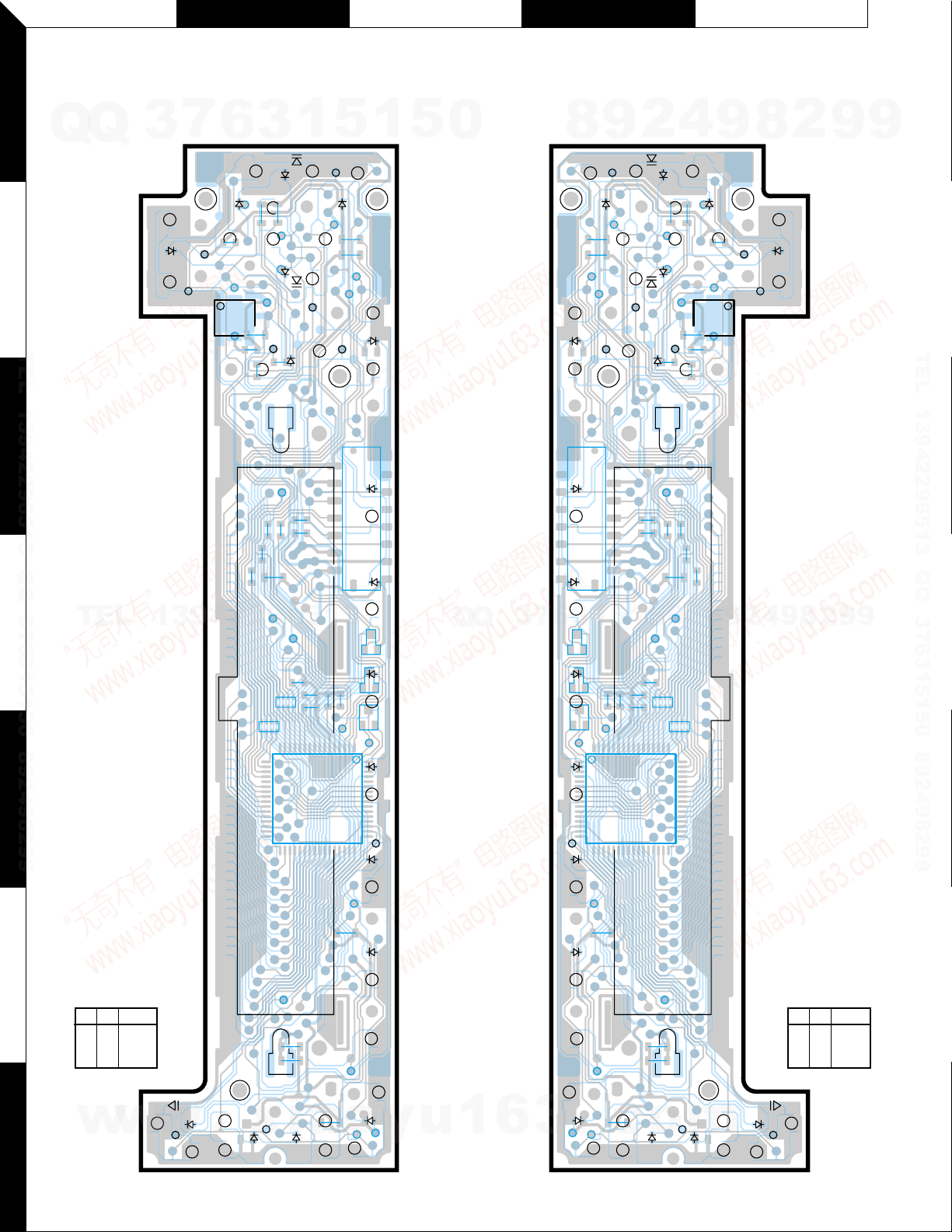
PC BOARD
(COMPONENT SIDE VIEW)
Q
Q
3
D17
SRC
7
X13-9680-1X (J74-0978-12)
6
D10
KI2
FM
C7
KS4
KI1
KI1
1
2
IC2
4
3
R13
SW5V
3
R19
REMO
C5
R11
R7
R9
KI3
R5
R10
KI3
R17
R12
PL1
D11
R3
1
KI4
D12
KI4
AUD
D16
RST
R4
R2
D13
KI5
5
KI5
AM
R16
R18
KS5
KS4
KS5
2
14
J1
D15
6
1
CLK
D14
AUTO
D9
(FOIL SIDE VIEW)
5
0
1
15
X13-9680-1X (J74-0978-12)
8
R16
R18
KS5
CLK
KS4
D14
AUTO
J1
1
D15
6
D9
15
9
KI5
AM
D13
KI5
KS5
2
14
D12
KI4
D16
2
D11
KI4
KI3
AUD
R12
PL1
RST
R4
R2
REMO
KI3
R3
R10
C5
R17
KI2
R13
R5
R19
C7
2
4
R7
FM
KI1
IC2
R11
R9
4
9
D10
1
3
SW5V
38
KS4
8
D17
SRC
KI1
2
9
9
TEL 13942296513 QQ 376315150 892498299
6
D8
Q1
KS6
KS3
3
D22
D23
4
D7
3
D6
2
ILL-GND
D5
1
RST
D4
.
LAMP+B
BE
1
16
5
1
L-DATAL
64
17
R15
PAN5V
ATT
R14
5
C1
c
KS2
IC1
R8
1
C2
C3
R20
R21
VOL
DWN
D3
5
D-GND
C4
o
L-CE
0
CP1
49
32
KS3
PL2
CP2
48
33
VOL
KS2
UP
m
D2
8
9
9
9
2
8
9
4
2
24 25
1
IC Q
address
15D
22E
15D
D1
KI2
R8
L-DATAL
IC1
KS2
C1
ILL-GND
R15
PAN5V
ATT
R14
o
5
D22
D23
EB
D7
16
D6
D5
RST
D4
1
D8
4
Q1
KS6
3
KS3
2
1
y
LAMP+B
u
Q
Q
1
3
6
7
3
4
5
6
TEL
IC Q
15B
22B
15C
w
7
13942296513
address
D1
w
w
KI2
.
L-CE
D-GND
C4
C2
CP1
C3
CP2
49 64
48
33
32 17
1242538
KS3
R20
R21
PL2
KS2
D2
VOL
DWN
D3
VOL
UP
xia
Refer to the schematic diagram for the values of resistors and capacitors.
8
 Loading...