Kenwood DPX-5010 Service manual
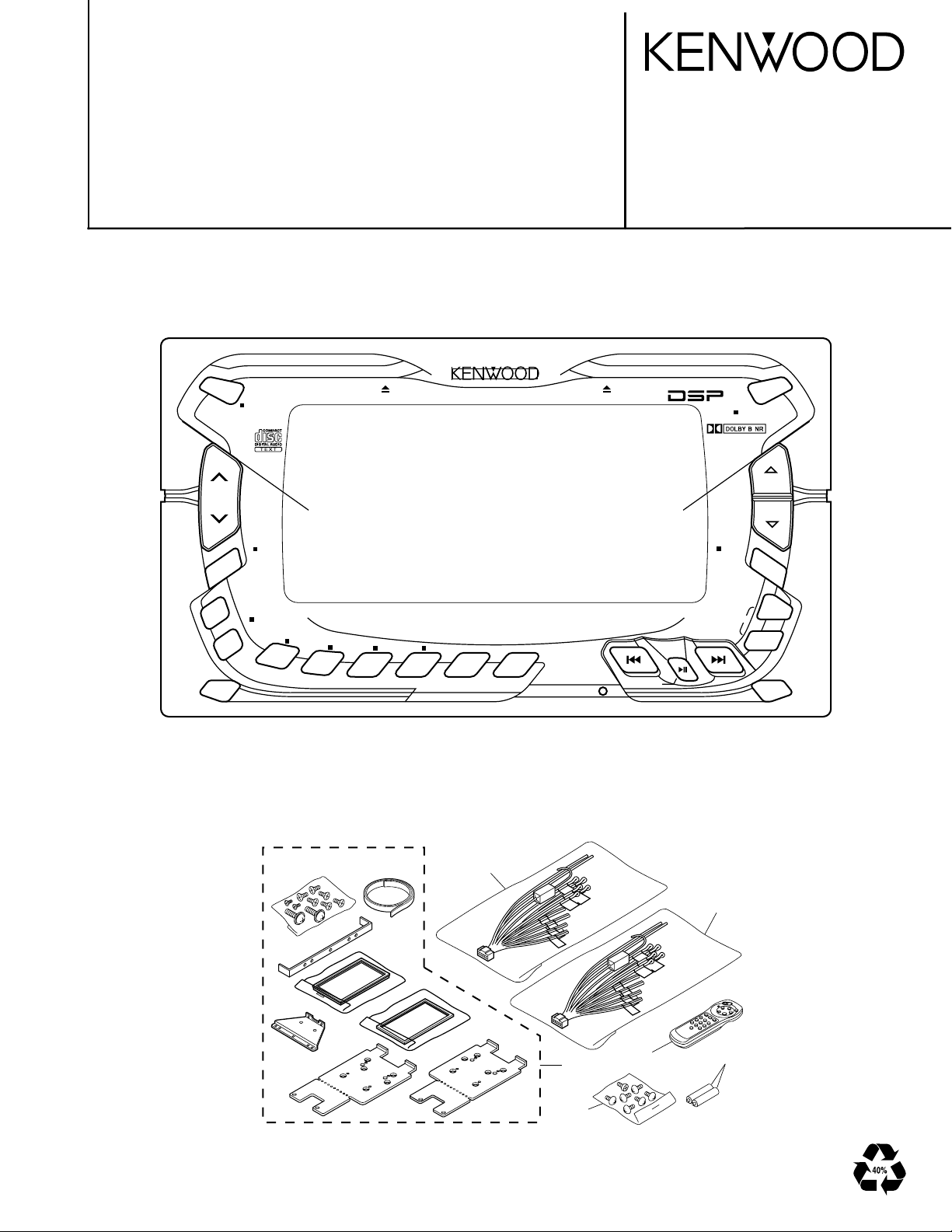
CD CASSETTE DSP RECEIVER
DPX-5010
SERVICE MANUAL
Refer to the service manual "D40-1132-05" (B51-7505-00)
for CASSETTE MECHANISM ASSY's information.
CD OPEN/CLOSE TAPE OPEN/CLOSE
© 2000-8 PRINTED IN JAPAN
B51-7663-00 (N) 1714
DSP
ATT
EQ
DISP
D
I
S
C
DIR AUD
DPX-5010
OFF PWR
VOLUME LAST ANGLE
CRSC SBF
NAME.S
SCROLL
B NR
7
1
D
I
R
E
C
T
SCN
8
2
COMPRESSION
KBS
RDM/B.S
9 0
34
SFC
POSITION
DBB
SFC LEVEL
REP M.RDM/MTL
ROOM SIZE
D.S
56
DIGITAL SIGNAL PROCESSOR
DIGITAL X,OVER
CD CASSETTE
DSP RECEIVER
MEMORY
PROGRAM
DISC
OFF
SRC
RETURN
ANGLE
FNC
FM
AM—
+
The following reference numbers with accessory parts are the same reference numbers
used on EXPLODED VIEW and PARTS LIST.
DC1
205
210
RM1
DC1
711

DPX -50 10
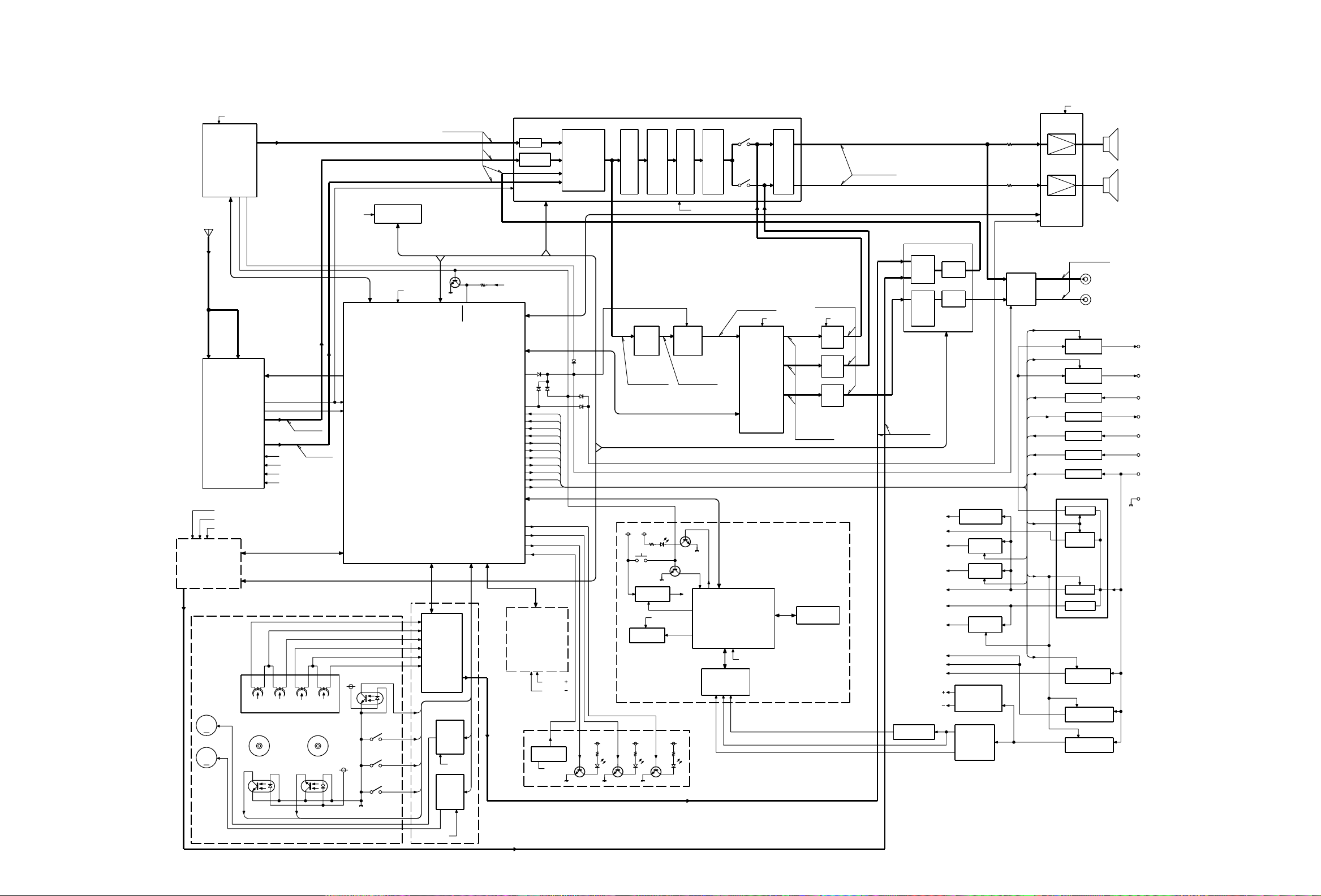
BLOCK DIAGRAM .................................................................................... 3
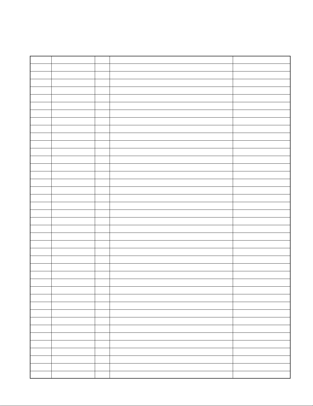
MICROCOMPUTER’S TERMINAL DESCRIPTION .................................. 5
PANEL MECHANISM DESCRIPTION....................................................... 9
TEST MODE / ADJUSTMENT................................................................. 11
PC BOARD .............................................................................................. 12
SCHEMATIC DIAGRAM .......................................................................... 21
EXPLODED VIEW ................................................................................... 30
PARTS LIST............................................................................................. 34
SPECIFICATIONS ............................................................... BACK COVER
CONTENTS
2
ANT.
CD MECHA
AUDIO OUT
CASSETTE
MECHA
MAIN
SUB
AM ANT
A2
M
M
B.U
MD/CD
CHANGER
FM DET OUT
AM DET OUT
BU 5V
AUD +B
SRV +B
SW1-3
AMUTE
MRST
MSTOP
LO/EJ
MOTOR
SDA
SCL
CLK
DATA
FM ANT
REQ
FSD
FM SD
Takeup Reel
F/E
CE
FWD
Lch
REELT
PON 5V
AUD +B
FM +B
AM +B
REV
Lch
PLAY HEAD
FM
FWD
::400mV
REELS
AM
160mV
REV
RchRch
Supply Reel
PON 5V
PLL CLK
PLL DATA
PLL CE
PLL REQ
FSD
FM SD
SW1-3
AMUTE
MRST
MSTOP
LO/EJ
MOTOR
IC14
REQC
REQH
DATA C
CH CLK
CH CON
DOLBY UNIT
(X30-3000-00)
MODE
PACK DET
STBY
PACK IN
E2PROM
DATA H
BU 5V
SYSTEM u-COM
MSC
MTL
MUSIC
EQ-MUTE
FWD/REV
DOLBY
F-IN(L)
VREF(L)
R-IN(L)
F-IN(R)
VREF(R)
R-IN(R)
HA12216F
IC2,Q4
CD CH
TAPE
FM
AM
SCL
SDA
FREEL
A OUT
MAIN
MOTOR
DRIVER
2SB
SUB
MOTOR
DRIVER
RREEL
PACK DET
IC1
BU
DPX -50 10 DPX-50 1 0
BLOCK DIAGRAM
PM DET
PM
OPEN-SW
PWIC STBY
PWIC SVR
DSP WRQ
DSP WRDY
PW MUTE
LINE MUTE
LED LOGO
LED TAPE
IC2
ISO
NC. MPX
+6dB
BU 5V
IC1
BEEP
TEST
DSP RST
DSP PD
DSP SO
DSP CLK
MUTE
BU DET
ACC DET
SMALL
ANT CON
P CON
P ON
FM
AM
ILLUM
FL PON
SCDATA
MCDATA
CTS
RTS
SC-CON
LED CD
CD PACK
REFCON
PANEL MECHA
SDA
PM DET
PM-MODE
OPEN-SW
MOTOR
MOTOR
CD PACK
PON 5V
SCL
CD CH
TAPE
FM
AM
INPUT
SEL
+2dB
:
+4dB
:
+0dB
:
+4dB
:
ILL+B ILL+B
E VOL, TONE, NC, MPX
SOFT
VOL
MUTE
Buff
1511mV
:
475mV
:
798mV
254mV
:
DOWN
-12.4dB
CD CH
TAPE
FM :
AM
ILL +BBU 5V
RST SW
SW 5V
5V SW
DTB123YK
SW 5V
IC3
REMOCON
ILL+B
TRE
MUTE&
LEVEL
-0.5dB
CD CH
TAPE
FM :
AM :
AUD +B
:
363mV
:
114mV
192mV
61mV
ED1
BASS
PANEL u-COM
VFD
CD CHFM:
TAPE
:
:
AM :
IC8
DSP
(+2.4-3dB)
DSP RST
DSP PD
DSP WRQ
DSP WRDY
DSP SO
DSP CLK
BU 5V
342mV
108mV
180mV
58mV
IC1
DSP 5V
1200mV
:
300mV
:
400mV
:
160mV
:
RESET
SUB+
MAIN
MODE 1-3
SUB-
REFCON
VOL
TAPE
+15dB
OTHER
+11dB
FRONT
REAR
CD CH
TAPE
FM
AM :
FRONT
LPF
BUFF
9dB
REAR
LPF
BUFF
9dB
N/F or
REAR
LPF
BUFF
9dB
IC9-11
319mV
CD CH
:
100mV
TAPE
:
169mV
:
59mV
AMFM:
SWITCH UNIT
(X25-8330-11)
KEY MATRIX
:
900mV
:
283mV
:
475mV
151mV
AUD +B
CD CH
TAPE
FM::
AM
:
3193mV
:
1593mV
1687mV
537mV
CD
TAPE
IC5
::1200mV
VDD
HPF MUX
AMP
TAPE
+15dB
OTHER
+11dB
300mV
DSP(A) 3.3V
DSP(D) 3.3V
FM +B
AM +B
AUDIO +B
BU 5V
PON 5V
CD SRV +B
MOTOR +B
ILL +B
MOTOR
MOTOR
FL
SDA
VOL
SCL
IC17
A1
IC18
DSP3.3V AVR
FM8V SW
AM8V SW
5V SW
PANEL
MOTOR1
DRIVER
+B
DC/DC
FAC
MUTE
-0.5dB
FM
AM
IC12
PWR AMP
TEST
STBY
SVR
BEEP
ANT CON
P CON
LINE MUTE
AMP-CTRL
SMALL
ACC DET
B.U DET
P ON
P ON2
L4943
ILLUM
B. U
CD CH
:
3014mV
TAPE
:
1503mV
:
1592mV
AMFM:
507mV
FRONT
PRE OUT
REAR/NON FAD
PRE OUT
ANT CON
P CON
LINE MUTE
AMP-CTRL
SMALL DET
ACC DET
BU DET
SW 14V
DSP3.3V
AVR
A8V AVR
D5V AVR
ILL +B AVR
SRV +B AVR
DC/DC +B SW
IC3
Q16
FRONT
SP OUT
REAR
SP OUT
ANT CON
P CON
LINE MUTE
AMP-CTRL
SMALL
ACC
B. U
GND
MOTOR +B
3 4
DPX -50 10
MICROCOMPUTER’S TERMINAL DESCRIPTION
(X14-) IC1 : System µ-com
Pin Pin Name I/O Description Processing Operation
1 DSP RVDT O DSP data output
2 DSP_CLK O DSP clock output
3 CHCON1 O External CH1 selection H: CH1, L: Others
4 CHCON2 O External CH2 selection H: CH2, L: Others
5 DATAH O External CH data output
6 DATAC I External CH data input
7 CHCLK I/O External CH clock input/output
8 BYTE I External data bus width switching
9 CNVss I Processor mode switching
10 DSP_REDY I DSP write request
11 DSP_RST O DSP Reset
12 Reset I Reset input L: Reset
13 Xout O Main system clock output
14 Vss I Power input
15 Xin I Main system clock input
16 Vcc I Power input
17 NC I Not in use
18 SP INT I Spectrum analyzer reception permission
19 B U DET I B.U detection H: Power down
20 REQC I External CH reception request
21 REQH O External CH transmission request H: On
22 PANT O Power antennal control H: On
23 PCON O External amp power control H: On
24 PON O Power control H: On
25 LAMP O Lamp control H: On
26 AMP_CTRL O External amp control H: On
27 A CC DET I ACC detection H: ACC off
28 B UZZ O Beep ouput
29 SCL O IC2 clock ouput
30 SDA I/O IC2 data input/output
31 PN MC DATA * O Panel µ-com communication data output
32 PN SC DATA I Panel µ-com communication data input
33 PN RTS O Panel µ-com communication control
34 PN CTS I Panel µ-com communication control
35 PMOT1 O Panel motor control
36 PMOT2 O Panel motor control
37 REFCON O A/D reference voltage output
38 PMDET I Panel mechanism detection
39 OPEN SW I Panel full-open detection L: Panel full-open
40 PM VR O Panel mechanism voltage congrol H: 5.1V, L: 7.2V
41 PN SCCON O Panel µ-com communication control line
H: Panel Microcomputer stop
5
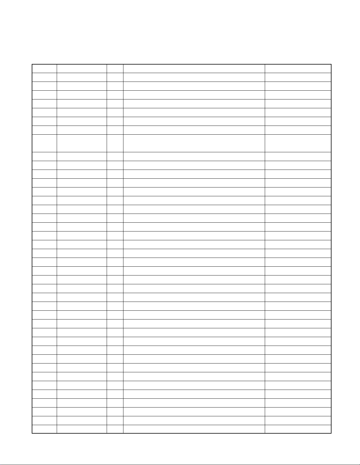
DPX -50 10
MICROCOMPUTER’S TERMINAL DESCRIPTION
(X14-) IC1 : System µ-com
Pin Pin Name I/O Description Processing Operation
42 MUTE O MUTE H: MUTE on
43 LED CD O LED CD display H: On
44 LED TAPE O LED T APE display H: On
45 LED LOGO O LED LOGO display H: On
46 SP_REQ O SPANA data output request to panel microcomputer
47 CD_SW3 I CD mechanism SW3 detection
48 CD MOTOR O CD loading motor control H: On
49 CD_LO/EJ I/O Loading/Eject control L: Loading direction
50 CD_MSTOP O CD mecha controller stop L: Stop
51 CD_MRST O CD mecha controller reset L: Reset
52 CD_AMUTE I CD mute request H: Mute request
53 CD_SW1 I CD mecha SW1 detection
54 CD_SW2 I CD mecha SW2 detection
55 TA DOLBY O Dolby selection SW H: DOLBY on
56 TA MTL O Metal selection SW H: Metal, L: Normal
57 TA_F/R O Play direction selection SW H: RWD, L: FWD
58 TA MUSIC I Between-music detection input SW L: Music
59 TP MSC O Casettee between-music selection SW L: FF&REV
60 TA EQ MUTE O EQ music selection SW H: MUTE on
61 SEL1 I IC2III noise cancellation selection
62 Vec - Power input
63 NC O Not in use L: Fixed
64 Vss - Power input
65 SEL2 I IC2III noise cancellation selection
66 SEL3 I Location switching H: M, L: J
67 NC O Not in use. L: Fixed.
68 PACK_DET I PACK detection SW L: PACK
69 TA_MODE1 I Cassette MODE1 detection SW
70 TA_MODE2 I Cassette MODE2 detection SW
71 TA_MODE3 I Cassette MODE3 detection SW
72 TA_SMOTOR1 O Cassette sub motor control 1
73 TA_SMOTOR2 O Cassette sub motor control 2
74 TA_MOTOR O Cassette main motor control H: On
75 NC O Not in use. L: Fixed.
76 PLL CLK O PLL clock ouput
77 PLL DATA I/O PLL data input/output
78 PLL_CE O PLL selection
79 FMSD I FM station detection H: Station
80 PLL_REQ O PLL seek selection L: In seek
81 FM+B O FM Power H: FM
H: Eject direction
6
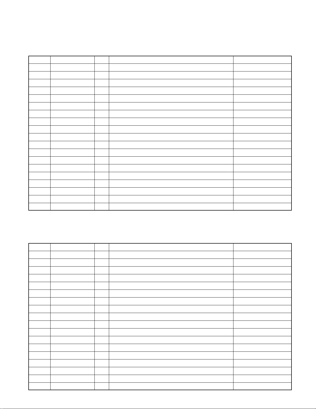
DPX -50 10
MICROCOMPUTER’S TERMINAL DESCRIPTION
(X14-) IC1 : System µ-com
Pin Pin Name I/O Description Processing Operation
82 AM+B O AM Power L: AM
83 PMUTE O Power IC MUTE control H: MUTE on
84 ILLUMI I Illumination detecton L: Dimmer on
85 LINE_MUTE I External MUTE request L: Line MUTE on
86 PCON_IN I External amp peak current control H: Protection on
87 NC O Not in use. L: Fixed.
88 PWIC SVR O Power IC control H: On
89 TEST O Power IC control L: In test mode
90 PWIC_STBY O Power IC standby H: On
91 F_REEL I Reel pulse (FWD) detection SW Vth: 2.5V
92 R_REEL I Reel pulse (RWD) detection SW Vth: 2.5V
93 TAPE_DET I Tape detection H: Tape (A/D input)
94 CD_DET I CD detection sensor input H: CD (AD input)
95 PMODE I Panel position sensor input (AD input)
96 Avss I Analog po wer input
97 FSD OUT I S-meter input H: Station (AD input)
98 Vref - A-D reference voltage input
99 Avcc I Analog po wer input
100 DSP_XLAT O DSP write request
(X25-) IC1 : Panel µ-com
Pin Pin Name I/O Description Processing Operation
1~3 NC O Not in use
4 REMO O Remote signal input
5 NC O Not in use
6 SP DATA O Spectrum analyzer data input
7 SP CLK O Spectrum analyzer clock input
8 BYTE - External data bus width selection
9 CNVss - Processor mode selection
10,11 NC O Not in use
12 RESET - Reset input
13 Xout - Main system clock output
14 Vss - Power input
15 Xin - Main system clock input
16 Vcc O Power input
17,18 NC O Not in use
19 SP REQ I Spectrum analyzer data input request
20 PN SC CON I System µ-com communication control line
21~23 NC O Not in use
24 GBK O FL dot section data blanking output
7
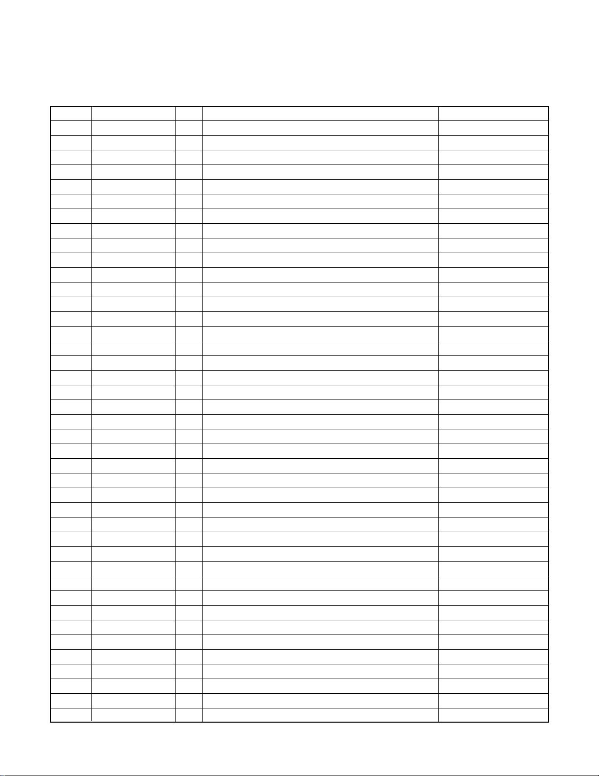
DPX -50 10
MICROCOMPUTER’S TERMINAL DESCRIPTION
(X25-) IC1 : Panel µ-com
Pin Pin Name I/O Description Processing Operation
25 GLAT O FL dot section data latch ouput
26~30 NC O Not in use
31 PN_SC_DATA O System µ-com communication data output
32 PN_MC_DATA O System µ-com communication data input
33 PN RTS O System µ-com communication control line
34 PN CYTS I System µ-com communication control line
35,36 NC O Not in use
37 GCLK O FL dot section clock output
38~61 NC O Not in use
62 Vcc - Power input
63 NC O Not in use
64 Vss - Power input
65 LED4 G O 4 key illumination (green) control H: On
66 LED4 A O 4 k ey illumination (red) control H: On
67 LED3 G O 3 key illumination (green) control H: On
68 LED3 A O 3 k ey illumination (red) control H: On
69 LED2 G O 2 key illumination (green) control H: On
70 LED2 A O 2 k ey illumination (red) control H: On
71 LED1 G O 1 key illumination (green) control H: On
72 LED1 A O 1 k ey illumination (red) control H: On
73 KR4 I Key Return signal input 4
74 KR3 I Key Return signal input 3
75 KR0 I Key Return signal input 0
76 KS4 O Key Scan output 4
77 KS3 O Key Scan output 3
78 KS2 O Key Scan output 2
79 KS1 O Key Scan output 1
80 KS0 O Key Scan output 0
81~88 NC O Not in use
89 KR5 I Key Return signal input 5
90 PON O Periferal IC pow er control H: On
91 KR1 I Key Return signal input 1
92 KR2 I Key Return signal input 2
93 TAPE_EJECT O TAPE EJECT key illumination selection L: Blue
94 CD_EJECT O CD EJECT key illumination selection L: Blue
95 NC O Not in use
96 A vss - Analog power input
97 SP_INT O Spectrum analyz er data control request
98 Vref - A-D referece voltage input
99 A vcc - Analog power input
100 NC O Not in use
8
1
2
3
4
312
304
308
304
309
320
321
316
303
302
305
DPX -50 1 0
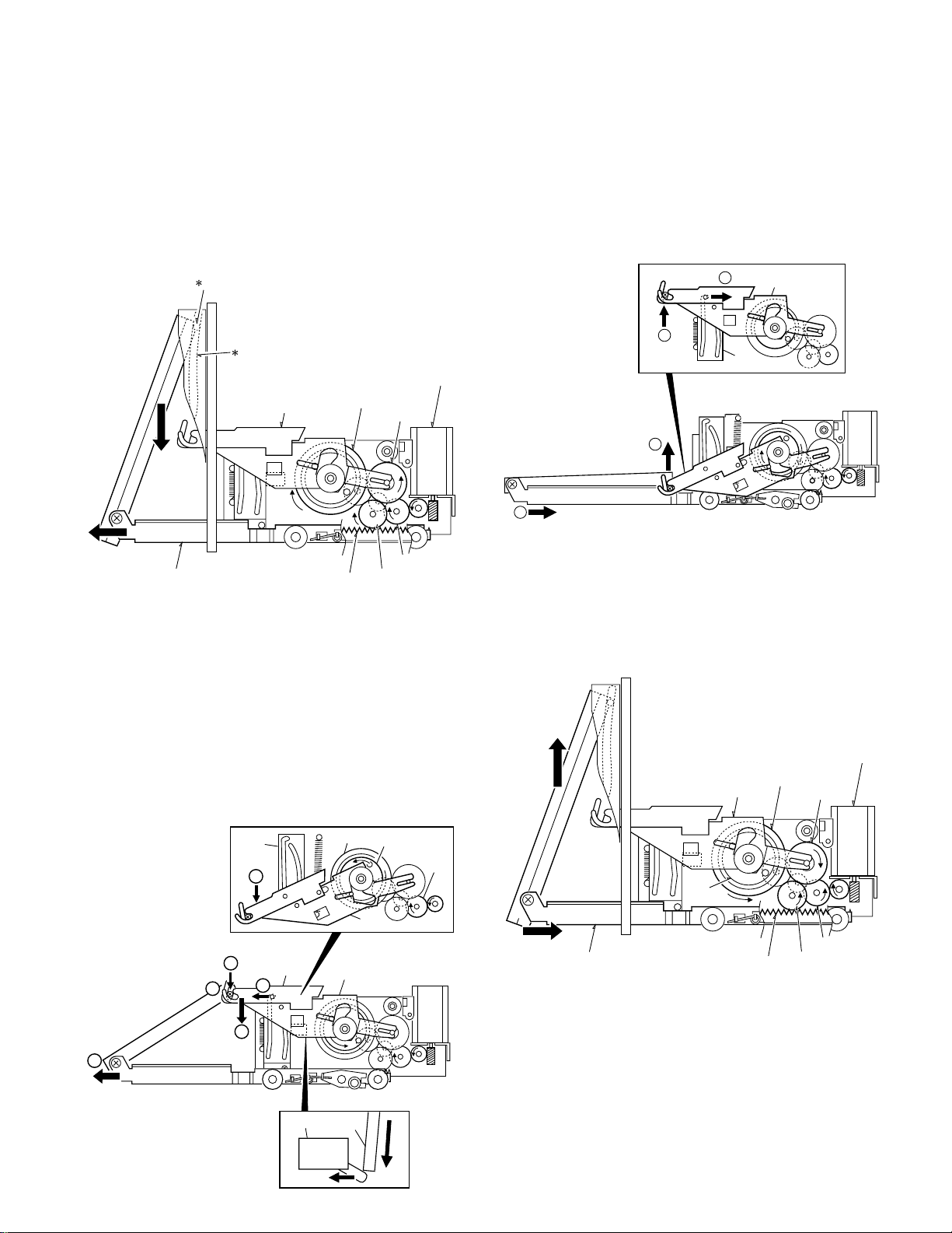
PANEL MECHANISM DESCRIPTION
A.Panel Opening
1. When Open button(switch) is pressed, the motor (305)
rotates.
2. The rotation of the motor is transmitted forward through
the rack gear (316) via the gears (320-322)
3. When the rack gear (316) moves, the panel (PA1) goes
down.
4. (1) The upper side of the panel pushed on the arm as-
sembly (304) by the pin (✽2) and the groove of the
rail (✽3).
(2) The lock on the lever (A) is let go and the arm assem-
bly (304) goes down.
(3) When this happens, the planetary gear (303) rotates.
5. When the arm assembly goes down to the open position,
the switch (341) is turned on. When the switch (341) is
turned on, the motor stops after 950ms.
302
2
3
305
316
308
309
320
321
304
B. Closing Behavior
1. The motor rotates in reverse direction.
2. The arm assembly (304) goes up. When the lever (A) goes
into the lock position of the rail (312), the arm assembly
(304) stops going up.
3. When the arm assembly (304) stops, by the rotation of
the planetary gear (303), the motor rotation pushes the
rack gear (316) backward via the gears (320-322).
4. By the close position information of the LPS (342), the
motor (305) stops after 200mS.
308
304
304
303
320
304
C. Angle Behavior
1. By the position information of the LPS (342), the panel
angle is controlled.
312
3
1
2
4
A
2
3
341
9
342
314
3
342
316
301
305
4
DPX -50 1 0
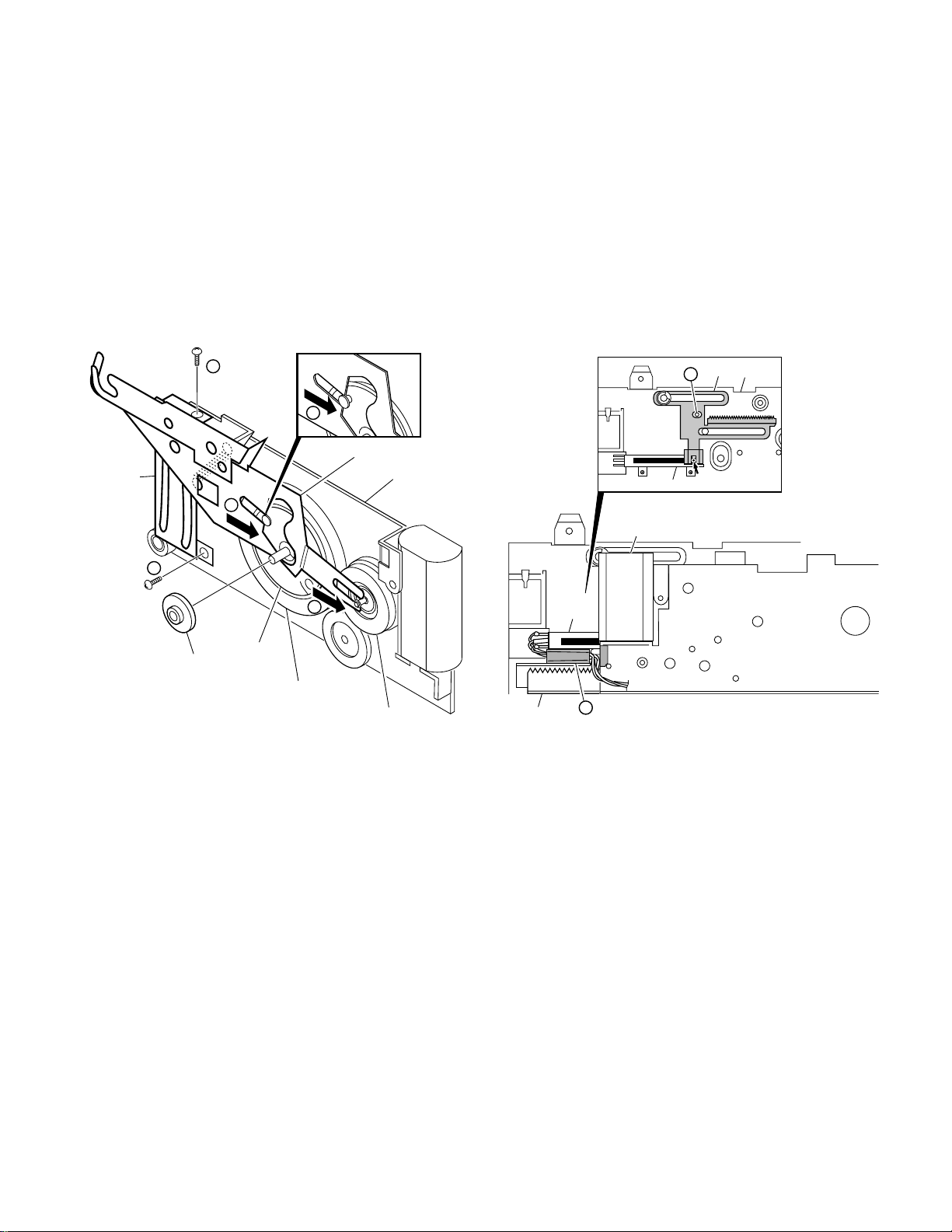
D.Assembly (Close Position)
1. Align the arm assembly with the pin of the planetary gear
(303).
2. Assembly these to the sub-chassis (306) along with the
rail (312).
3. Align lever (314) hole and the hold of the chassis (301).
4. Lead wires of LPS should be kept in place with a tape so
that they would not interfere with rack gear (316).
2
312
1
PANEL MECHANISM DESCRIPTION
1
304
306
2
325
1
303
308
309
10

DPX -50 10
TEST MODE / ADJUSTMENT
■ How to enter the text mode
While pressing on 1 and 3 keys, press the RESET key.
■ Panel Mechanism Adjustment
The mechanism detects the open/close position of the panel
and writes it to the E2PROM.
■ Starting on the test mode
Major initial positions
•
When booted with everything off, the test mode starts up.
• The valueof the volume is –40dB (indication is 15).
• FL lamps all light up.
• The diversity is off.
• Position: All.
• EQ: Flat
• COMPRESSOR: OFF
• SPE/ANA: PEAK HOLD
■ All display lamps lighting up
Since there are many segments on the display section,
bridging with other segments can be confirmed. By track up/
down keys, grids and segments can be lighted up individually.
■
Opening/Closing Time of the Panel Mechanism
When each time the Angle/Retune button is pressed, time
is displayed after going into the tuner mode. From the maximum angle to return, it takes about 1.2S.
■ CD Mechanism Panel Disk Detection
Sensor behavior for detecting whether there is CD disk or
not can be checked. When the sensor is closed off after a
disk is inserted, it beeps four times.
■
FM S-Meter Adjustment (Stop Adjustment and others)
Method:
SG Output: Set to 35dBµ 98.1MHz. (with no modulation)
During the above text mode, when Preset 1 and Preset 6.
are pressed at the same time, the adjustment begins. When
adjustments is completed normally , OK is displayed and there
will be one beep of 2kHz. In this case the stop adjustment
values will be between 15~25dBµ.
When the S-meter value is outside of the standard system
control values, NG is displayed and the initial value of the
system control is written in the E2PROM.
■ AM Stop Adjustment
Method:
SG Output: Set to 35dBµ 999kHz. (with no modulation)
During the above text mode, when Preset 1 and Preset 6.
are pressed at the same time, the adjustment begins. When
adjustments is completed normally , OK is displayed and there
will be one beep of 2kHz. In this case the stop adjustment
values will be between 30~43dBµ .
When the S-meter value is outside of the standard system
control values, NG is displayed and the initial value of the
system control is written in the E2PROM.
[ How to enter the test mode ]
After entering the above-mentioned test mode, switch over
to the tuner mode. Then, press on the TI knob for some time
and the unit will go into panel mechanism test mode, which
is indicated by STAND-BY display.
Method:
Each time Open/Close key (*key) of the remote controller
is pressed, full-open and full-close positions are registered.
(There will be OPEN ENTRY/ CLOSE ENTRY display and
three beeps are sound.)
Releasing:
When TI key is pressed, the unit goes back to the previous
test mode. Pressing the reset key will take the unit to the
initial condition.
■ DOLBY Adjustment
Using the extension cord (W05-0755-00), separate the
mechanism from the unit. Play the TCC-130 and adjust the
test round value to 300mV with the VR1, 2 on the X30 Board.
(Refer to the PC BOARD.) Balance with FWD and REV.
■ Releasing the Security Code
The unit will go into release mode when Preset 6 is pressed
while Preset 1 is being pressed. The character “C” is displayed at the right end of the character display. At this point,
input KCAR by using 1, 2, 3, and 4 key of the remote controller. Confirm with PLAY/PAUSE key and the security code will
be released.
■
The bass boost function of the amplifier can be remote
control from the unit. This is a one-way communication, using one control line. The control is made with pulse widths of
the three kinds of communication data. Five cycle pulses are
generated from the unit side and when there are three consecutive successes, comm unication is established. The pulse
widths are as shown below and the cycle is 200ms.
HI: 100ms
LOW: 70ms
OFF: 40ms
Specifications for the Amplifier Control Terminal
11
11
A B C D E
1
2
3
4
5
6
PC BOARD
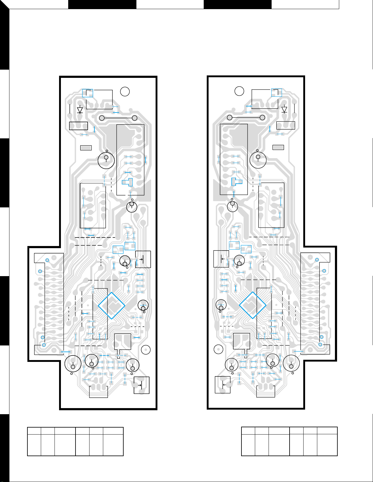
(COMPONENT SIDE VIEW)
DOLBY NISE REDUCTION UNIT
X30-3000-00 (J74-0940-22)
BE
GND
L
Q5
14
D1
R19
BE
R18
BU
R27
CN2
2
J8
R13
24
J7
C15
1
23
R
J6
R16
J5
R10
C6
R17
J9
C10
R8
R1
1
C25
9
R15
J3
C8
R6
C1
Q4
J2
W2
R12
15
C20
11
10
C28
C4
R4
W4
2
8
J4
C12
W3
W1
C26
C2
R2
C19
CN3
20
1
W9
J1
R25
IC1
CN4
R23
Q1
EB
21
40
W5
R24
C22
R26
S1
C3
R3
D2
W8
R22
R21
C21
C16
C7
31
C23
EB
30
W7
C11
R14
C13
W6
10
R20
IC2
1
C18
C17
Q2
C9
R11
R9
C5
R7
C14
J10
R5
C27
Rch
VR2
VR1
Lch
(FOIL SIDE VIEW)
DOLBY NOISE REDUCTION UNIT
X30-3000-00 (J74-0940-22)
Q5
14
C20
W1
2
8
9
J2
J3
J4
W2
11
10
C8
R12
W3
C26
C28
C4
R4
W4
C1
51
EB
Q4
1
C10
R1
C25
R16
J5
R10
D1
BE
R18
R17
R15
J9
J6
R13
C6
J7
R8
R6
VR1
Lch
J10
10
1
R11
R9
C5
R7
VR2
R20
IC2
C14
R5
Rch
W6
C18
Q2
C9
C17
C27
R22
R21
C21
R14
C13
CN4
R24
C22
R23
C19
J1
D2
C23
CN3
C16
Q1
E
E
B
B
C12
R26
C7
30
31
R25
20
21
IC1
1
40
C11
S1
W9
W8
C3
C2
R2
R3
W5
W7
R19
CN2
J8
C15
2
24
R27
BU
1
GND
L
23
R
CN1
X30-3000-00
IC Q Address
15B
7
23B
14B
IC Q Address
24B
42B
52B
Refer to the schematic diagram f or the
values of resistors and capacitors.
X30-3000-00
CN1
IC Q Address
IC Q Address
15D
23D
14D
24D
42E
52E
12
F G H I J K L M N O
1
2
3
4
5
6
7
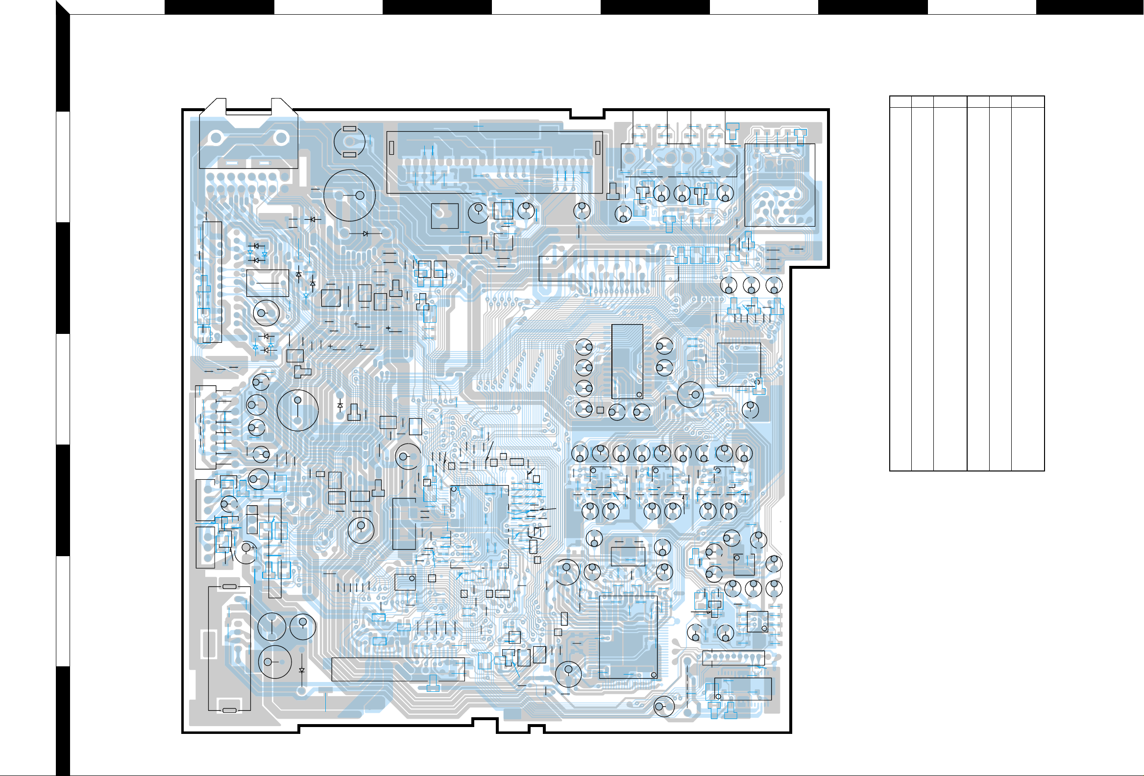
PC BOARD (COMPONENT SIDE VIEW)
SYNTHESIZER UNIT
X14-602x-xx (J74-0920-52)
J1
16
8
C221
25
C220
24
C234
C235
D39
C222
R196
R195
IC12
EB
Q49
2
1
TH1
Q48
EB
R197
R207
R208
C38
14
IC3
R20
C15
C10
R19
R17
R23
C11
R22
R21
R24
2
Q15
R25
B
B
E
E
E
Q17
Q16
C32
Q22
B
D16
E
E
B
Q24
BE
Q25
R31
C42
R35
A1
15
1
B
C17
C20
C33
C31
B
Q23
C233
E
R32
7
1
D49
D42
D46
D44
D47
C14
C12
C9
C26
C24
R26
22
D14
BE
C35
C34
C47
2
C40
L1
C36
D48
C19
Q28
C21
CN3
C41
R10
D43
C16
EB
BEBE
D17
C7
C22
Q29
9
R199
D45
21
R34
R33
B
E
1
1
C27
R4
D9
R204
R42
Q14
Q27
D8
EB
Q26
D50
R13
D7
R198
Q50
C2
R203
D10
R43
D18
C8
Q9
Q13
R201
R202
C13
D11
C39
R14
L10
W1
BE
R200
C232
E
R36
D2
Q12
B
EB
C23
C151
C254
R306
1
D1
R12
C229
D3
IC18
IGO
C167
R305
C264
Q10
R18
C231
EB
C150
C263
Q54
Q53
D23
C1
R9
R27
R1
L29
R301
IC15
R259
EBE
EBE
R8
EB
Q11
Q1
C240
R7
C230
BE
X2
A2
D4
R41
D24
4
R3
C3
5
Q55
CN5
C6
C241
R219
R226
R233
C246
1
R16
R5
R2
C242
R218
C243
EBE
L5
C5
D6
R44
R6
C4
R212
R315
8
R249
Q5
E
Q2
BE
R227
R251
1
R239
C64
B
EB
R214
CP3
EB
Q52
C244
CP5
R234
R240
R53
L4
D40
R221
R325
Q4
EB
D5
R216
R211
R210
R326
R324
R222
R228
R328
R241
C66
L7
BE
Q3
R213
R248
R232
R323
30
R304
CP13
R242
R243
R244
C71
R247
1
31
R319
D25
Q6
C256
CP6
100
C255
C245
R220
R250
29
R238
R308
IC1
R246
R224
R229
C253
R245
C63
Q32
R215
R307
R309
R296
C74
R45
C73
EB
R312
R223
R314
R303
R318
R317
R253
EB
Q51
Q35
R237
C257
R310
R316
CP7
C72
L6
B
R51
BE
R50
R49
R217
R225
CP4
C248
R273
C262
C249
R298
R300
CP8
R252
R322
R327
4
31
B
CP14
81
R278
R311
R302
1
4
IC14
Q34
E
C261
80
R283
R282
R286
51
50
5
D41
E
R52
C77
Q33
C76
CP9
R284
R280
R276
R321
R313
IC16
5
Q60
C146
D26
C187
8
C177
C157
C212
D30
R90
5
C173
C158
R182
Q46
R91
R151
C145
C149
L20
D35
C216 C217
R190
R186
E
D38
C84
Q37
EB
C111
C110
C123
C185
C196
R160
R143
R162
R139
R137
C92
D34
R76
C91
R111
B
Q41
R109
C135
R40
C50
R183
B
R71
R166
R164
C190
E
R107
R191
R187
E
B
C82
Q38
BE
C116
23
C109
33
C108
C199
4
C194
C192
C93
R75
R110
BE
R106
25
Q36
BE
C214
C215
R189
R188
R285
C69
CN2
15
J3
D12
C210
R184 R185
R180
B
C218
D37
EB
R181
Q44
E
Q45
C211
242
14
C113
C75
R47
R46
R48
C68
C67
L8
123
C70
24
L9
C100
IC5
C101
C184
R136
R135
C155
L18
C104
C122
C153
L17
100
C56
1
R150
R142
C178
4
C176
R138
X1
C143
1
C189
IC10
C172
R113
31
L19
C166
C163
C114
L30
C179
30
1
C259
R320
8
C258
C247
EB
R231
R265
R275
CP12
Q59
R264
CP10
R268
R272
CP11
EB
R269
R271
C260
R274
R281
R279
L28
L27
R270
R277
C169
CP1
C251
C102
C103
R144
R134
C168
CP2
C165
C182
C159
C252
C124
R152
R140
L12
C140
4
C180
C174
C170
L14
C141
C164
1
L13
80
CP16
C188
51
IC9
C175
50
28
C186
R153
C171
C148
C152
C142
C160
C161
81
C105
8
5
C154
C144
R114
L16
C106
C125
C183
R145
C181
R141
L15
R112
C156
IC8
C162
D15
D13
C219
C213
Q47
C88
C83
R63
D27
R65
C85
C86
D32
R95
D33
R94
C117
22
C119
IC2
R92
C198
C107
1
8
R167
IC11
R165
5
C195
C193
C191
R77
C90
C94
18
IC13
C133
4
C132
R100
Q42
C128
5
R102
R108
C134
8
R104
C130
C55
C52
IC17
C53
1
D21
R69
C81
C118
12
4434
C197
R161
R163
IC7
5
R61
D29
R96
19
C51
R64
R66
R67
R68
C87
C121
11
1
C112
C95
C126
R101
4
R105
1
C131
CN1
C54
13
C120
D36
C129
R103
14
R62
J2
C96
D31
C127
R60
R70
D28
X14-602x-xx
IC Q Address
15I
24L
34G
54K
76L
86K
95K
10 5K
11 5L
12 3G
13 6L
14 6J
15 6I
16 6J
17 7L
18 5H
14I
24I
33I
53I
63I
93H
10 3H
11 3H
12 5H
13 5H
14 5H
15 5G
16 5G
17 5G
IC Q Address
23 5G
24 5G
25 5G
26 6H
27 5H
28 5G
29 5G
32 3I
33 3J
34 2J
35 2J
36 7L
37 3K
38 3L
41 6K
42 6L
44 2K
45 2K
46 2K
47 2L
48 4G
49 3G
50 4H
51 6I
52 5I
53 6H
54 6H
55 6I
59 6J
60 6J
22 5G
Refer to the schematic diagram for the values of resistors and capacitors.
14
 Loading...