

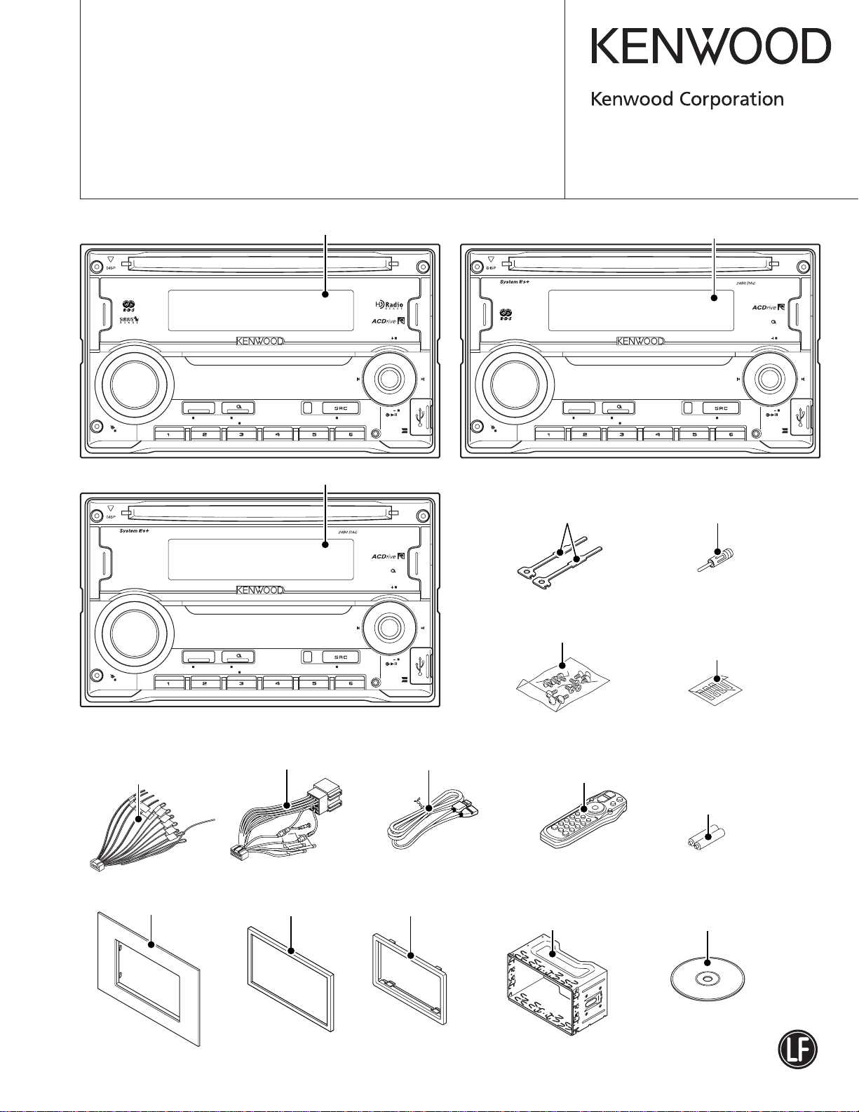
2DIN CD RECEIVER
DPX501/501 U/501UY
DPX-MP2090U
SERVICE MANUAL
© 2006-4 PRINTED IN JAPAN
B53-0400-00 (N) 960
DPX501 (K type) DPX501U/501UY (E type)
EXTERNAL MEDIA CONTROL
AUTO
VOL
AUD
SET UP
ATT
MENUAME
DPX-MP2090U (M type)
Panel assy (A64-3814-02)
DPX501
FM SCRL
USB
PTY/C.S.
SWAM
OFF
F.SEL
REPRDM A.RDMSCANS.MODE
M.RDM
Panel assy (A64-3966-02)
EXTERNAL MEDIA CONTROL
TI
VOL
AUD
SET UP
ATT
Lever (K,E type)
(D10-4589-04) x2
DPX-MP2090U
System
EX
FM SCRL
EXTERNAL MEDIA CONTROL
Screw set (K,M type)
(N99-1779-05)
AUTO
VOL
AUD
SET UP
ATT
MENUAME
REPRDM A.RDMSCANS.MODE
OFF
F.SEL
M.RDM
SWAM
USB
Panel assy (A64-3871-02)
DPX501U
System
EX
FM SCRL
SWAM
MENUAME
REPRDM A.RDMSCANS.MODE
OFF
F.SEL
M.RDM
/PTY
USB
Antenna adaptor (E type)
(T90-0523-05)
Adhesive doublecoated tape (K,E type)
(H30-0595-04)
DC cord
(E30-6408-05):(M type)
(E30-6414-05):(K type)
Escutcheon (K,E type)
(B07-3172-12)
DC cord (E type)
(E30-6412-05)
Escutcheon (M type)
(B07-3046-04)
Cord with connector(USB)
(E30-6535-05)
1.5m
Escutcheon (K,E type)
(B07-3165-02)
Remote controller
assy (K,M type)
(A70-2067-15)
RC-527
Mounting hardware
assy (K,E type)
(J22-0429-13)
This product uses Lead Free solder.
SIZE AA BATTERY(K,M type)
(Not supplied)
Compact disc
(W01-1673-05):(K,M type)
(W01-1674-05):(E type)
DPX501/501U/501UY
DPX-MP2090U
● Complete view
ELECTRIC UNIT (X34- )
CN5 IC9
OPEL DISP
MARINE RC
OEM RC
A1
TUN8V
SW5
AM+B
J2
LX-BUS
3
IC1
713
IC7
RESET
BU5
J4
J1
S3
RESET
IC2
REMOTE
SW5
S1
ROTAR Y
ENCODER
SWITCH UNIT (X16- )
F/E
FST
SW5
RDS
W1
BU
CN
Q6
SW5V
SW5
A8V
PRE+B
PREF
SYSTEM u-COM
2
PAN5V
PAN5
CN4
AUX IN
IC2
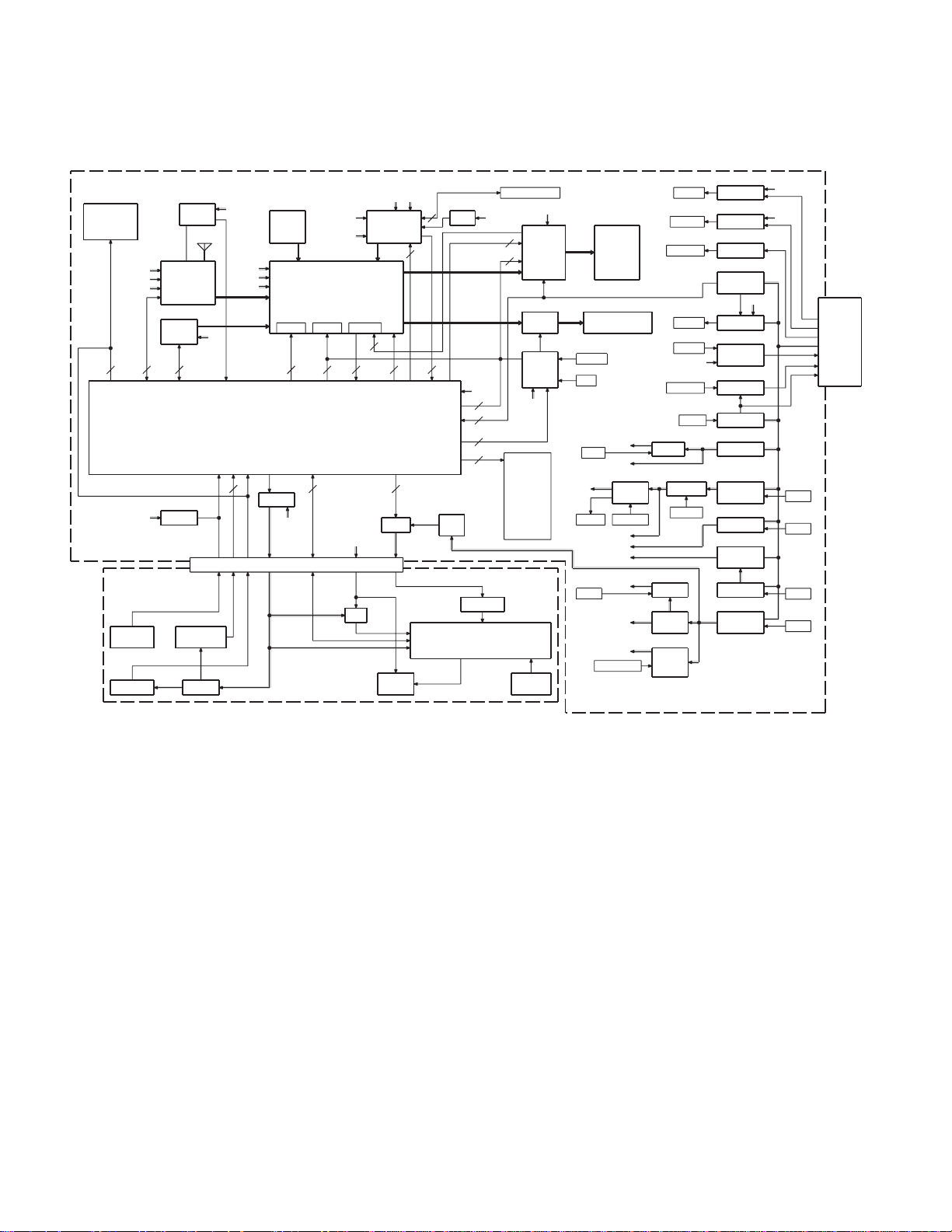
BLOCK DIAGRAM
A8V
SERVO+B
E-VOL
MUTE
MUTE DC-DET
1
38
5
Q13
BU5
ILLUMI+B
SW
DME1
CD MECHA
1
1
FL+B
KEY
ILLUMI
BU5V
D5V
CN2,3
2
USB
USB5
2
10
BU5
1
1
2
9
IC13
3/4W
Rx10
R73
ED1
1/2W Rx1
DRIVER & KEY MATRIX BUILT-IN,NEW
COLOR
SELECT
VFD
PON USB/C DET
BU
IC4
3
PW-IC
1
Q400-405
MUTE
IC6
MUTE
LOGIC
BU5
DC-CN etc
PHONE
DIMMER/
ACC DET
BU DET/
ANT CON
P CON/P ON
P ON CD/
P ON ILLUMI
P ON FL/
EX-AMP
2DIN
KEY
MATRIX
J1
FRONT L/R
REAR L/R
NF L/R
J3
PRE-OUT
FRONT/REAR/(NF)
Q111
BU DET
Q114
RST
P ON
USB5
SERVO+B
AM+B
ILLUMI+B
PON ILLUMI
SP-OUT
SW5
BU5
IC8
HISIDE
SW
PON USBC DET
D5V
A8V
AM+B
TUN8V
Q3,11
Q300,301
Q302,303
Q305,306
ACC DET
ANT CON
SW5V
AM+B
TUNER
8V
SW
ILLUMI
+B
PHONE
DIMMER
BU DET
EX-AMP
BU5
P CON
CD5V
PON CD
C104,D107,R112
PHONE
Q108
DIMMER
Q112
ACC-DET
Q109
SURGEDET
BU5
Q111
BU-DET
Q107
EXT-AMPCON
Q101,102
ANT-CON
Q103,106
PCON-SW
Q1,2
BU5V
Q12,21IC12
SURGE
SW20V
Q5,6,10
A8V
Q7,8
CD
SERVO
Q4,9
SW14V
IC5
ILLUMI
+B
BU5
BU5
P ON
P ON
P ON
P ON
J1
DC-CN
PHONE
ILLUMI
ACC
B.U.
EXT-CONT
P-ANT
P-CON
2
(
)
y
(
)
(
)
(
)
(
)
CS EMPH
(
)
(
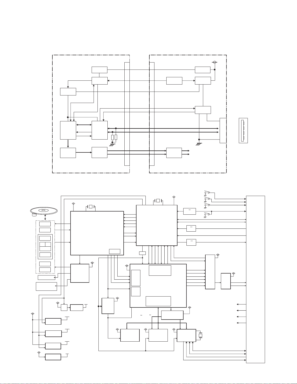
● AC Drive + USB Mechanism unit
IC19
BU3.3V
IC1
Mecha-
uCOM
IC20,21
CS3.3V
CS1.8V)
P-ON
BLOCK DIAGRAM
SYS-
uCOM
H/U
P-ON
30Pin FFCDXM-6810W/DXM-6820W CD_Mechanism
CN1
BU5.0V
/MSTOP
D5.0V
DPX501/501U/501UY
DPX-MP2090U
BU14V
BU5.0V
5V
SW-Reg.
/CS RST
IC15
DECODER
/INT
/RESET
IC18
● CD player unit (X32-583)
SW3.3V(712)
DPU1
LD
PD
E
BA
C
F
D5V(D4V)
TR COIL
FO COIL
SP MOTOR
Loading & sled
MOTOR
CS POW
POWER
IC5
3.3V Reg.
IC21
3.3V Reg.
IC20
1.8V Reg.
BU5V
IC19
3.3V Reg.
A8V
SW
SW3.3V(712)
CS3.3V
(CS7410)
CS1.8V
(CS7410)
BU3.3V
IC4
IC14
Motor
Driver
5V Reg.
SW A5V
IC25
USB
DRIVER
IC13
LFP
16.893M
RF AMP
SERVO DSP
IC2
S7.5V
IC28
3STATE
BUFFER
I2S
CS3.3V
CS7410
CS3.3V
CS7410
PowerON SW
Over Current
USB_D+
USB_D-
L-ch
R-ch
CS POWER
POW ON
A0
SI
STB
SCK
/RESET
SO
INTQ
DA_EMPH
delay
CS3.3V &
CS1.8V
DATA
LRCK
BCLK
C16
CKO
/CSRST
CD I/F
PLL
DRAM
4,8,16bit
256K
/NV_CS
CS3.3V
CS7410
IC16 IC17
SDRAM
64Mbit
1M*4B*16bit
/CSRST
11.500MHz
µ-COM
IC1
S_DAT
B_DAT
CLK
DATA_MUT
SREQ
SER2(3/4Wire)
BREQ
ACD DECODER
MP3/WMA/AAC
DECODER
IC15
Memory
Controller
ROM
8bit
0
2MB
Memory
Flash
8Mbit
1M*8bit
NAND
GATE
EVOLDAC
CS3.3V
CS7410
BU3.3V
/CS , A20
Q7
3.3 5V
(SW3.3V)
Q6
3.3 5V
(
BU5V
Q3
3.3 5V
(BU5V)
IC26
/USB_CS
USB
DRIVER
)
Infinit
0 Det.
EMPH
DAC_RST
DAC_MUTE
PCM_XCK
PCM_DATA
PCM_LRCK
PCM_BCLK
CS3.3V
CS7410
VBUS 5V
High-side
Switch
6.00MHz
IC25
USB_
USB_D+
USB_D-
USB
IC18
DAC
5V
GND
SW A5V
IC13
LPF
Cable
LOS-SW
12EJE-SW
8EJE-SW
LOE/LIM-
I2CDATA
CCLK
/I
2
SW A8V
Audio_Lch
Audio_Rch
D5V(D4V)
USB_D+
USB_D-
/OC
/PO
BU5
A8V
S7.5
USB CONNECTOR
CN1
To
MAIN
BOARD
3

DPX501/501U/501UY
DPX-MP2090U
COMPONENTS DESCRIPTION
● ELECTRIC UNIT (X34-415x-xx)
Ref. No. Application / Function Operation / Condition / Compatibility
IC1 System µ-COM
IC2 E-VOL Controls the source, volume, tone.
IC3 A8V REF Power Supply Outputs 1.27V.
IC4 Power IC Amplifies the front L/R and the rear L/R to 50W maximum.
IC5 ILLUMI+B Power Supply Outputs 11.25V.
IC6 Muting Logic IC Controls logic for muting.
IC7 Reset IC “Lo” when detection voltage goes below 3.6V or less.
IC8 Hi-side SW
IC9 RDS IC Decodes RDS.
IC10 Installer Memory IC Installer memory.
IC12 SW Regulator Supplies power for USB and CD mechanism.
IC13 FL+B Power Supply Outputs 3.0V.
Q1,2 B.U.5V AVR While BU is applied, BU5V AVR outputs +5V.
Q3,11 SW5V When Q11’s base goes “Hi”, SW5V outputs +5V.
Q4,9 SW14V When Q9’s base goes “Hi”, SW14V outputs 14V.
Q5,6,10 AUDIO8V AVR When Q10’s base goes “Hi”, A8V AVR outputs 8.0V.
Q7,8 SERVO+B AVR When Q8’s base goes “Hi”, S+B AVR outputs 7.5V.
Q12,21 Serge Protect for IC12 Outputs 20V when BU is over 20V.
Q13 PANEL5V When the base goes “Lo”, PANEL5V outputs 5V.
Q17 IC12 ON/OFF When the base goes “Lo”, IC12 is “ON”.
Q101,102 P-ANT SW When Q102’s base goes “Hi”, P-ANT SW outputs 14V.
Q103,106 P-CON SW When Q106’s base goes “Hi”, AVR outputs 14V.
Q104,105 P-CON Protection
Q107 EXT-AMP-CON When the base goes “Lo”, Q107 is turned on.
Q108 Small Lamp DET SW When the base goes “Hi”, Q108 is turned on.
Q109 Serge DET When the base goes “Hi”, IC4 is changed into standby source.
Q111 BU DET When the base goes “Hi”, Q111 is turned on.
Q112 ACC DET When the base goes “Hi”, Q112 is turned on.
Q113 Mute Driver When the base goes “Hi”, pre-out mute driver is turned on.
Q116 Pre-out Mute Driver When the base goes “Lo”, mute driver is turned on.
Q300,301 AM+B When Q301’s base goes “Hi”, AM+B is output.
Q302,303 Tuner8V When Q303’s base goes “Hi”, Tuner8V outputs 8V.
Q305,306 SW ILLUMI+B When Q306’s base goes “Hi”, SW ILLUMI+B outputs 11V.
Q400~403
Q406,407
Q408 Pre-out Mute ON/OFF When the base goes “Lo”, pre-out mute is "ON".
Pre-out Mute SW When the base goes “Hi”, pre-out is muted.
Controls FM/AM tuner, the changer, CD mechanism, panel, volume and tone.
Over current protection of USB power supply.
When pin 1 goes “Hi”, USB5V is ON.
Output protection is applied when P-CON output voltage fall is detected.
The 2 transistors protect Q103 false operation when P-CON SW is “ON”.
4
DPX501/501U/501UY
DPX-MP2090U
COMPONENTS DESCRIPTION
● SWITCH UNIT (X16-353x-xx)
Ref. No. Application / Function Operation / Condition / Compatibility
IC1 Remote Control IC
Q1~3 GRID_DRIVER Each transistor’s base is “L” then GRID is on.
Q6,7 SW5V The power supply of IC1 is turned on when Q6’s base level goes “L”.
Q8 DBO LED SW DBO LED is turned on when Q8’s base level goes “H”.
Q9 RED SW RED LED is turned on when Q9’s base level goes “H”.
Q12 VFD Restart Key scan start at Q12’s base goes “H”, when the set’s power is on.
● CD PLAYER UNIT (X32-5830-00)
Ref. No. Application / Function Operation / Condition / Compatibility
IC1 Mechanism µ-com
IC2 Signal Processor
IC4 BTL Driver Spindel motor, sled (including loading & eject) motor and pick-up actuator
IC5 SW3.3V Regulator 3.3V power supply for IC2, pick-up, IC18 digital part
IC13 Audio Active Filter 2nd LPF
IC14 A5V Regulator 3.3V power supply for DAC
IC15 DSP for Compression Audio Decoder ACDrive decoder, MP3/WMA/AAC decoder
IC16 Compression Audio Codec SDRAM
IC17
IC18 Audio D-A Converter (24-bit external) External 24-bit for audio
IC19 BU3.3V Regulator 3.3V power supply for µ-com
IC20 1.8V Regulator 1.8V power supply for IC15 core part
IC21
IC25 USB Host Controller
IC26
IC28 Clock SW To SDRAM
Q3 Level Shift 3.3V→5V
Q6,7 Level Shift 3.3V→5V
Q8 APC (Auto Power Control)
Q9,10 Anticipation Sub-beam Delay During non-searching
Q17 USB Hi-side SW
D2 Static Electricity Countermeasure For IC2 built-in reset terminal
D3 Laser Diode Protection
D9 Static Electricity Countermeasure
Decoder Software &
Unique ID Strage Flash ROM
Decoder/SDRAM/Flash ROM/ Power supply for decoder, SDRAM, flash ROM and USB driver.
USB Driver 3.3V Regulator 3.3V power supply for IC15 port parts, IC16, IC17, IC25, IC26 and IC28.
Switching among IC15 & Flash ROM &
SDRAM & USB
For DSP for Compression Audio Decoder, Flash ROM, SDRAM and USB
5
DPX501/501U/501UY
DPX-MP2090U
MICROCOMPUTER’S TERMINAL DESCRIPTION
● SYSTEM MICROCOMPUTER: 30624MWPA86GP (X34: IC1)
Pin No.
1 REMO I Remote control signal input Detects pulse width
2 LX MUTE I Mute request from slave unit H: Mute ON, L: Mute OFF
3AUD SDA O E-VOL data output
4AUD SEL O E-VOL control
5AUD SCL O E-VOL clock output
6 BYTE 7 CNVSS 8 XCIN I
9 XCOUT I
10 RESET 11 XOUT 12 VSS 13 XIN - 12.0MHz
14 VCC1 15 NMI - Not used
16 CN DET I
17 RDS CLK I RDS decoder clock input
18 LX REQ S I Communication request from slave unit
19 PON AM I/O AM power supply control H: Receiving AM, Hi-z: No AM
20 LX REQ M O Communication request to slave unit
21 TUN IFC OUT I Front-end IFC-OUT input H: Station found, L: No station
22 NC - Not used L fixed
23 RDS AFS M I/O Noise detection time constant switching q Refer to the truth value table
24 RDS QUAL I RDS decoder QUAL input
25 RDS DATA I RDS decoder data input
26 PWIC BEEP O Beep output
27 TUN SCL I/O Front-end I2C clock input and output MAX400kHz
28 TUN SDA I/O Front-end I2C data input and output
29 VFD DATA I/O VFD data input and output
30 VFD INT I VFD INT input INT input
31 VFD CLK O VFD clock output Normal: 125kHz, Low consumption mode: 62.5kHz
32 VFD RST O VFD driver reset L: Momentary power down, panel detached or 11
33 ROMCOR SDA I/O
Pin Name I/O Application
Panel communication detection
(Flip-down panel model only)
E2PROM I2C data input and output for
ROM correction
Truth
Value Table
Processing Operation Description
H: Panel detached, L: Panel attached
H: Canceling reset, L: Reset
minutes after ACC OFF
6
DPX501/501U/501UY
DPX-MP2090U
MICROCOMPUTER’S TERMINAL DESCRIPTION
Pin No.
34 ROMCOR SCL I/O
35 PON PANEL I/O
36 DSI I/O
37,38 NC - Not used L fixed
39 EPM I Flash EPM input
40 PANEL DET I
41 NC - Not used L fixed
42 ROMCOR DET I E2PROM writing request H: Writing
43 PON FL O FL+B control H: FL+B ON, L: FL+B OFF
44 VFD CS O VFD chip select control
45 ROTARY CW I VOL key input Detects pulse width
46 ROTARY CCW I VOL key input Detects pulse width
47 CD DISC12 SW I 12cm CD detection
48 CD LOS SW I CD loading detection
49 CD MUTE R I Rch CD mute request H: Normal, L: Requesting Rch mute
50 CD MUTE L I Lch CD mute request H: Normal, L: Requesting Rch mute
51 CD MRST O CD mecha µ-COM reset H: Normal, L: Reset
52 CD MSTOP O CD mechanism µ-COM stop H: Mecha µ-COM operates, L: Mecha µ-COM stops
53 CD DISC8 SW I 8cm CD detection (Not used)
54 CD LOE LIM SW I CD detection (Chucking SW) H: Loading completes, L: No disc
55 CD LOEJ I/O CD motor control w Refer to the truth value table
56 CD MOTOR O CD motor control w Refer to the truth value table
57 PON ILLUMI I/O Key illumination power supply control H: ON, Hi-Z: OFF
58 PON CD O Power supply control for CD-WMA
59 PON O Power supply H: POWER ON, L: POWER OFF
60 VCC2 61 EXT AMP CON I/O EXTERNAL AMP control
62 VSS 63~65 TYPE 1~3 I Destination switching e Refer to the truth value table
66 TUN TYPE1 I Destination setting 1 r Refer to the truth value table
67 TUN TYPE2 I Destination setting 2 r Refer to the truth value table
68 OEM DISP DATA I/O
Pin Name I/O Application
E2PROM I2C clock output for
ROM correction
Panel 5V control
(Flip-down panel model only)
DSI/EJECT LED control OFF: Hi-z, Pulse drive: Panel detached
(Flip-down panel model only) H: Illumination ON or panel opened (POWER ON)
Panel detection (Flip-down panel model only)
External display data
(Destination K and E only)
Truth
Value Table
Processing Operation Description
L: ON
Hi-Z: Momentary power down, panel detached or 11
minutes after ACC OFF
L: Panel detached, H: Panel attached
L: POWER ON, H: POWER OFF
L: Before M-STOP with reset
External display
7
DPX501/501U/501UY
DPX-MP2090U
MICROCOMPUTER’S TERMINAL DESCRIPTION
Pin No.
69 OEM DISP CLK I/O
70 OEM DISP CE I/O
71 EJECT I
72 P CON O External amplifier control H: POWER ON, L: POWER OFF or STANDBY
73 VFD KEY REQ I Communication request from VFD driver Connects to INT
74 ANT CON O Power antenna control Tuner ON: H
75 ILLUMI DET I Dimmer illumination detection L: ON, H: OFF
76 BU DET I Momentary power-down detection L: BU found, H: No BU or momentary power down
77 ACC DET I ACC power supply detection L: ACC found, H: No ACC
78 (PWIC SVR) O SVR discharging circuit
79 PWIC MUTE O Power IC mute L: STANDBY, momentary power down or TEL mute
80 PWIC STBY O Power IC standby control H: POWER ON, L: POWER OFF
81 LX CON O Start-up request to slave unit H: Slave unit starts up, L: Slave unit stops
82 MUTE PRE R O Rch preout mute
83 MUTE PRE L O Lch preout mute
84 MUTE 0 I/O E-VOL front mute L: Mute ON, Hi-Z: Mute OFF
85 MUTE 1 I/O E-VOL rear mute L: Mute ON, Hi-Z: Mute OFF
86 MUTE 2 I/O E-VOL mute (Except front/rear)
87 LINE MUTE I Line mute detection
88 MUTE PRE SW I/O NF preout mute
89 PWIC DC DET I DC offset error detection
90 LX RST O Forced reset to slave unit H: Reset, L: Normal
91 MUTE C I/O E-VOL mute L: Mute ON, Hi-Z: Mute OFF
92 NC - Not used L fixed
93 RDS NOISE I FM noise detection
94 AVSS 95 TUN SMETER I S-meter input
96 VREF - Connects to P.ON
97 AVCC - Connects to VCC
98 LX DATA S I Data from slave unit
99 LX DATA M I/O Data from and to slave unit
100 LX CLK I/O LX-BUS clock
Pin Name I/O Application
External display clock
(Destination K and E only)
External display control request
(Destination K and E only)
Eject key input (Flip-down panel model only)
Truth
Value Table
Processing Operation Description
External display
External display
L: Eject
H: POWER OFF or 5 seconds after momentary
power down, L: Other conditions
CD MUTE R is Lo: H (CD playing), Momentary power
down: H, L: DUAL ZONE or NAVI INT
CD MUTE L is Lo: H (CD playing), Momentary power
down: H, L: DUAL ZONE or NAVI INT
TEL mute: Below 1V
NAVI mute: Over 2.5V
L: Mute ON, Hi-Z: Mute OFF
OFF fixed: Selecting REAR in REAR/SUB selection
8
MICROCOMPUTER’S TERMINAL DESCRIPTION
Truth value table
q AFS CONTROL
RDS AFS M Condition
AFS LOW L No sound output with AF search
AFS MID L Sound output with AF search
AFS HIGH Hi-Z Normal reception
w CD MOTOR CONTROL
CD MOTOR CD LOADING/EJECT
Stop L L
Load H L
Eject H H
Brake H Hi-z
DPX501/501U/501UY
DPX-MP2090U
e DESTINATION SW
TYPE 3 TYPE 2 TYPE 1
(Pin 65) (Pin 64) (Pin 63)
000KKDC-X590
001KKDC-MP632U
010EKDC-W6534U/UY
011EDPX501U/UY
100MKDC-X7533U
101MDPX-MP2090U
110KDPX501
111JDPX-U077
r TUNER TYPE
Kenwood brand model L L
OEM model 1 L H
OEM model 2 H L
OEM model 3 H H
DESTINATION MODEL
TUN TYPE1 TUN TYPE2
(Pin 66) (Pin 67)
9
DPX501/501U/501UY
DPX-MP2090U
MICROCOMPUTER’S TERMINAL DESCRIPTION
● MECHANISM MICROCOMPUTER: M30620FCPGP (X32: IC1)
Pin No. Pin Name I/O Application Processing Operation Description
1~5 NC - Not used Opened output L fixed
6 BYTE I External data bus SW input Connects to GND
7 CNVSS I Processor mode SW
8 MUTE O Audio mute control L: Mute ON, H: Mute OFF
9NC-Not used Opened output L fixed
10 RESET I Reset detection L: Reset (Flash ROM writing), H: Normal
11 XOUT O Main clock output Connects to resonator
12 VSS - Power supply input Connects to GND
13 XIN I Main clock input Connects to resonator
14 VCC1 - Power supply input Connects to BU3.3V
15 NMI I NMI interruption input Input Hi (Pull-up) fixed
16 MSTOP I STANDBY comeback interrupption L: Stop, H: Stop cancelled (Hi edge)
17 NC - Not used Opened output L fixed
18 DSP INT I DSP interruption signal input H: Interruption (Hi edge)
19~22 NC - Not used Opened output L fixed
23 E2P SCL I/O E2P I2C clock output
24 E2P SDA I/O E2P I2C data input and output
25,26 NC - Not used Opened output L fixed
27 SCL I System µ-com I2C clock input
28 SDA I/O System µ-com I2C data input and output
29 DSP TXD O Data output for DSP serial data Flash ROM writing: TXD (Pull-up)
30 DSP RXD I Data input for DSP serial data Flash ROM writing: RXD
31 DSP CLK O Clock output for DSP serial data Flash ROM writing: SCLK(Pull-up)
32
33 CS SDATA O Data output for decoder serial data
34 CS BDATA I Data input for decoder serial data
35 CS CLK O Clock output for decoder serial data
36~38 NC - Not used Opened output L fixed
39 EPM - Not used (Flash ROM: EPM) Opened output L fixed
40 PON D3.3 O D3.3V POWER ON control H: POWER ON, L: POWER OFF
41 PON A5 O A5.0V POWER ON control H: POWER ON, L: POWER OFF
42 PON CS1 O IC15 series 3.3V POWER ON control H: POWER ON, L: POWER OFF
43 PON CS2 O IC15 series 1.8V POWER ON control H: POWER ON, L: POWER OFF
44 CE - Not used (Flash ROM: CE) Opened output L fixed
45 DRV MUTE O Driver mute L: Stop, H: Mute OFF
46,47 NC - Not used Opened output L fixed
DSP STB (BUSY)
O DSP data strove signal output Flash ROM writing: BUSY
L: Single chip mode
H: Microprocessor mode or flash ROM writing
Series resistors and E2PROM are not built when
ROM collection is not used.
Series resistors and E2PROM are not built when
ROM collection is not used.
10
DPX501/501U/501UY
DPX-MP2090U
MICROCOMPUTER’S TERMINAL DESCRIPTION
Pin No. Pin Name I/O Application Processing Operation Description
48 ZERO M I 0-bit mute detection
49 DE-EMPHASIS O DAC de-emphasis control H: De-emphasis ON, L: De-emphasis OFF
50,51 NC - Not used Opened output L fixed
52 LIM SW I
53 DISC NORMAL O Media discrimination result output (Not used) H: Normal disc, L: Other disc
54 DISC H RW O Media discrimination result output (Not used) H: High reflecting RW disc, L: Other disc
55 DISC RW O Media discrimination result output (Not used) H: Normal RW disc, L: Other disc
56~59 TEST OUT4~1 O Output for test Opened output L fixed
60 VCC2 - Power supply input Connects to BU3.3V
61 TEST OUT0 O Output for test Opened output L fixed
62 VSS - Power supply input Connects to GND
63~66 NC - Not used Opened output L fixed
67 TEST IN3 I TEST IN3 Pull-down connection (L: Normal/H: During test)
68 MODEL SEL I Model determination L: DXM-6810W (X32-583), H: DXM-6820W (X32-587)
69 E2P WRITE I TEST IN1: E2P writing permission Pull-down connection (L: Normal/H: During writing)
70 UNIQ ID I TEST IN0: Uniqe ID writing permission Pull-down connection (L: Normal/H: During writing)
71~73 NC - Not used Opened output L fixed
74 SEARCH O Searching situation output H: During seaching, L: Normal
75,76 NC - Not used Opened output L fixed
77 DSP RST O DSP reset control L: Reset, H: Normal
78 DSP A0 O
79 DA EMPHASIS I DSP DA emphasis input H: emphasis ON, L: emphasis OFF
80
81 DATA MUTE O Data output status L: During data output muting, H: During data output
82 CS RST O Decoder reset control L: Reset, H: Nornal
83 NC - Not used Opened output L fixed
84 SREQ O Decoder SREQ signal output
85 BREQ I Decoder BREQ signal input
86~93 NC - Not used Opened output L fixed
94 AVSS - Analog power supply input Connects to GND
95 NC - Not used Opened output L fixed
96 VREF - Reference voltage input Not used: Connects to GND
97 AVCC - Analog power supply input Connects to BU3.3V
98~100 NC - Not used Opened output L fixed
ROM EMPHASIS
Laser pick-up inner circumference detection
SW signal input
DSP command/parameter discrimination H: During parameter transmitting
signal output L: During command transmitting
I Decoder ROM emphasis input H: emphasis ON, L: emphasis OFF
H: Mute ON, L: Mute OFF
(No distinction of Lch/Rch)
H: Inner circumference
11
DPX501/501U/501UY
DPX-MP2090U
TEST MODE
●How to enter the test mode
In order to enter the test mode, reset the unit while simultaneously pressing down [1] and [3] keys.
(Even when the security is set, power can be ON for 30 minutes.)
●How to clear the test mode
The test mode is cleared in case of any of the following e vents:
resetting, momentary power down, Acc OFF and Pow er OFF.
●Initial conditions of the test mode
• Source is STANDBY.
• Displays lights are all turned on.
• The volume is at –10dB (The display is 30).
• Loudness (LOUD) is OFF.
• CRSC is OFF, regardless of whether there are switching
functions or not.
• SYSTEM Q is NATURAL (=FLAT).
• BEEP will sound anytime with a less than 1 second push.
• Auxiliary (AUX) is ON.
• SWPRE is Sub woofer (2 PREOUT model)
●RDS/RBDS automatic measurement
Conventionally, the PS display has been visually checked on
the production line. This will be replaced by a new processing.
The PS data will be received and the PS contents is to be
verified as “RDS_TEST”. When this is verified, the P-CON
terminal is forced to go OFF. (In this case, “ _ ” means blank.)
→ This will be a dedicated test mode processing.
On the P-CON, when power is turned off once and, then,
turned on again, (Power OFF → ON) the unit will be restarted.
●Forced switching of K3I
In TUNER FM mode, each time [6] key is pressed, the functions move in the following cycle :
AUTO → forced WIDE → forced MIDDLE → force NARROW
→ AUTO
The initial condition is AUTO and the displays below will appear.
• AUTO : FM1_98.1A
• Forced MIDDLE : FM1_98.1M
• Forced WIDE : FM1_98.1W
• Forced NARROW : FM1_98.1N
●CD source test mode specifications
• Display mode default setting shall be P-TIME.
•Jumps are made to the following tracks by pressing the
[ ] key.
No. 9 → No. 15 → No. 10 → No. 11 → No . 12 → No. 13 →
No. 22 → No. 14→ No. 9 (Returns to the beginning)
It must be noted, however, that when paying MP3 / WMA /
AAC disk, which contain 8 files or less, the first track and
the following trac ks are played in order.
• When [ ] key is pressed, it goes down by 1 track.
• When playing an MP3/WMA/AAC disc, display the file format before starting to play each file. (“MP3”, “WMA”, “AA C”)
• When a CD is used as a source, by pressing [1] key f or less
than 1 second, a jump to the Track No. 28 is made.
• When a CD is used as a source, by pressing [2] key f or less
than 1 second, a jump to the Track No. 14 is made.
• When a CD is used as a source, by pressing [3] key f or less
than 1 second, a display of CD mechanism model name
and its version is made. When the pressing of [3] key for
less than 1 second is made for the second time, the normal
display is resumed. (Time code display)
●Special display when set to TUNER
When in TUNER mode, if any of the following displays appear,
there is an abnormality with the front end.
• “TNE2P_NG” : Front-end E2PROM values are still default
(not determined).
•“TNCON_NG” : In this condition, the communication with
the front-end is not possible.
12
6810:0123
Model name Version
• When a CD is used as a source, by pressing [6] key f or less
than 1 second, a jump to the Track No. 15 is made. At the
same time, the volume value is set to 25 (2V PRE).
TEST MODE
DPX501/501U/501UY
DPX-MP2090U
●Test mode specification for USB source
• While in USB source, by [6] key, set the volume value to 15.
●Audio adjust mode
•By pressing [AUD] key for less than 1 second, the Audio
Adjust mode is entered.
• As with the [AUD] key, [∗] key on the remote controller can
be used to enter the Audio Adjust mode.
• As for the adjustment items, items for both the AUDIO
FUNCTION MODE and SETUP MODE are included.
• By pressing [AUD] or [FM] key briefly, switch the item to be
adjusted in the following order. (only in forward rotation)
The initial item will be Fader, which is followed by : Balance
→ Bass Lev el → Middle Level → Treb le Le v el → HPF Front
→ HPF Rear → LPF Sub Woofer (After this, it will be arbi-
trary)
• With the remote controller, continuous forwarding is prohibited.
• Using the V OL knob and [ ] / [ ] key, the Fader can be
adjusted in 3 steps : R15 ↔ 0 ↔ F15 (The initial value is 0)
• Using the VOL knob and [ ] / [ ] key, the Balance can
be adjusted in 3 steps : L15 ↔ 0 ↔ R15 (The initial value is 0)
• Using the VOL knob and [ ] / [ ] key, the Bass / Middle
/ Treble Level can be adjusted in 3 steps : –8 ↔ 0 ↔ +8
(The initial value is 0)
• Using the VOL knob and [
Rear can be adjusted in 2 steps : Through ↔ 220Hz (The
initial value is Through)
• Using the VOL knob and [
Woofer can be adjusted in 2 steps : 50Hz ↔ Through (The
initial value is Through)
• Using the VOL knob and [
Phase can be adjusted in 2 steps : Re verse ↔ Normal (The
initial value is Normal)
• Using the VOL knob and [
set can be adjusted in 2 steps : –8 ↔ 0 (The initial value is
0)
• Using the VOL knob and [
ON/OFF can be adjusted in 2 steps : OFF ↔ ON (The
initial value is OFF)
• Using the VOL knob and [
can be adjusted in 2 steps : OFF ↔ ON (The initial value is
OFF)
• Bass f / Bass Q / Bass EXT / Middle f / Middle Q / Treble f
do no appear in audio adjustments.
] / [ ] key, the HPF Front /
] / [ ] key, the LPF Sub
] / [ ] key, the Sub Woofer
] / [ ] key, the Volume Off-
] / [ ] key, the Loudness
] / [ ] key, 2-Zone ON/OFF
●MENU items
• Press [Q] key briefly to enter the MENU.
• The [DNPP/SBF] and [DIRECT] keys on the remote controller can also be used to enter the MENU.
• With the remote controller, continuous forwarding is prohibited.
• When a CD/USB is used as a source, the default item will
be the F/W Version.
●2-ZONE (Dual Zone) items
• When using sources other than the STANDBY source, using a short-press on [AUTO] or [TI] key, 2-ZONE ON/OFF
is achieved.
●Backup current measurement
When reset in Acc OFF (Back Up ON) condition, MUTE terminal goes off after 2 seconds, instead of 15 seconds. (During
this time, the CD mechanism does not function.)
●OPEL communication items (OPEL communica-
tion specification supporting model)
During the test mode, OPEL communication line outputs the
following (At every 500msec, the output condition of the communication line will be switched.)
CE
DATA
CLK
500msec
500msec
500msec
●Special display when all lights are on
When all lights are on with the STANDBY source, the following displays are made when the ke ys shown below are pressed.
[1] key Version is displayed (forwarding)
(Display) TYPE : x___ (“x" is displayed hexadecimally)
→ 529K–1.02
→ All indicators on →
∗ TYPE indicates µ-com destination, and shows real-time
condition of the destination terminal
(“Development name” – “Version”)
13
DPX501/501U/501UY
DPX-MP2090U
TEST MODE
[2] key Serial number display (8 digits)
(Display) xxxxxxxx
[3] key Key pressed briefly : Power ON time is displayed.
(Display) PON_0Hxx (00~50 is displayed for “xx”.
When less than 1 hour, displayed
by increments of 10 minutes.)
xxxxx (00001~10922 is displayed for
“xxxxx”.) MAX 10922 (times)
During Power On time display, by pressing for at least 2
seconds, the Power ON time is cleared.
[4] key Key pressed briefly : CD operation time is displayed.
(Display) CDT_0Hxx (00~50 is displayed for “xx”.
When less than 1 hour, displayed
by increments of 10 minutes.)
xxxxx (00001~10922 is displayed for
“xxxxx”.) MAX 10922 (times)
During CD operation time display, by pressing for at least
2 seconds, CD operation time is cleared.
[5] key Key pressed briefly : CD EJECT number is displayed.
(Display) EJCxxxxx MAX 65535 (times)
During CD EJECT number display, by pressing for at
least 2 seconds, CD EJECT number display is cleared.
[FM] ROM correction version display
key (Display) ROM_R123
When E2PROM is not installed : ROM_ERR_
When un-written : ROM_R – – –
When data is incompatible : ROM_R ∗ ∗ ∗
[ ]AUDIO data default value setting
key (Display) AUD_INIT
[ ]Key pressed briefly : Forced Power OFF data displayed.
key(Display) POFF_ - - - (No Forced Power OFF)
SEC (Forced Power OFF because of
missing Security Code)
PNL (Forced Power OFF because of
system µ-com panel communica-
tion error)
While the forced power OFF data is displayed, press and
hold for 2 seconds to clear the data.
[ ]
Key pressed briefly : CD information display mode ON/OFF
key While in CD information display mode, press and hold for
2 seconds to clear all CD information.
∗ Please refer to the table right.
●CD information display mode
Displays I2C communication status.
(Display) I2C_OK__
NG
Displays CD loading error data.
(Display) Load_Error____
(Display) __ (1) xx__ (2) xx (number of times is displayed
for “xx”)
MAX 99 (times)
Disk detection switch ON/OFF is monitored, and when
the loading operation is not completed within the specified
time length, or when E-99 mechanism error occurred,
record which SW signal had an error.
∗Refer to the note at the end of [CD LOAD error detection].
[AM] Displays CD ejection error data.
key (Display) Eject_Error___
↑ (Display) __ (1) xx__ (2) xx
(Display) __ (3) xx__ (4) xx (number of times is displayed
for “xx”)
MAX 99 (times)
Disk detection SW ON/OFF is monitored, and when the
ejection operation is not completed within the specified
time length, or when E-99 mechanism error occurred,
record which SW signal had an error.
∗Refer to [CD EJECT error detection]’s note.
Displays CD time code count error data (missing count).
(Display) Count_Lose
↓ (Display) __CDDA_ : xx
[FM] (Display) __CDROM : xx (number of times is displayed
keyfor “xx”)
MAX 99 (times)
Monitor time code continuity. Record the number of times
when discontinuity occurred as error data.
Record the data of compressed audio and CD-DA played
separately.
Displays CD time code count error data (count not updated).
(Display) Count_Stay
(Display) __CDDA_ : xx
(Display) __CDROM : xx (number of times is displayed
for “xx”)
MAX 99 (times)
When the time code is not renewed for 2 or more seconds,
record the number of times occurred as error data
(skipped sound).
14

TEST MODE
DPX501/501U/501UY
DPX-MP2090U
●Initializing AUDIO-related value setting
During STANDBY sourcing, by pressing [ ] key for less than
1 second, AUDIO setting values are retur ned to the default
values.
●Other
• At Power ON, “CODE_OFF”, “CODE_ON” displays will not
be made.
• When the source is ST ANDBY, press [AUTO] / [TI] ke y briefly
to switch triangle illumi RED ↔ GREEN. (In models with
Display Blackout function)
•When the source is STANDBY, press and hold [AUTO] /
[TI] key for 1 second to s witch PREOUT Rear ↔ Sub Woofer .
(2PREOUT model)
• When in USB source, press [1] key briefly to turn ON/OFF
the front grass indirect lighting.
• When staring up in the test mode, LINE MUTE prohibition
time is set to 1 second instead of 10 seconds.
• While in the test mode, security jig should not be used to
write the security code.
• While in the test mode, serial writing jig should not be used
to write the serial number.
• While in the test mode, even when a DC offset error is detected, the detection information will not be written to the
E2PROM.
• While in the test mode, even after an elapse of pre-set time,
the backup memory items will not be written to the E2PROM.
• While in the test mode, backup/installer memory information clear mode, CD mechanism error log information clear
mode and DC offset error detection information clear mode,
DEMO mode operation will not be conducted.
Also, in the above mode , the menu of the STANDBY source
will not display DEMO ON/OFF switching items.
●Clearing backup/installer memory and CD mecha-
nism information, and service inf ormation (Clear ing E2PROM data)
Backup/installer memory X34-IC10 (E2PROM) “AU_”
CD mechanism information and service information: TUNER
F/E (E2PROM) “CD_”
1. While pressing and holding the [Q] key and the [ATT] key,
reset-start to start backup/installer memor y data, and CD
mechanism and service information initialization.
(Even when the security is set, power can be ON for 30
minutes.)
[CD mechanism information]
•Displays I2C communication condition
• Displays CD mechanism error log
• Displays CD loading error data.
• Displays CD ejection error data.
• Displays CD time code error count data (missing count).
•Displays CD time code error count data (count not updated).
[Service Information]
•Displays power ON time is displayed.
•Displays CD operation time.
• Displays number of CD EJECT times.
• Displays number of times panel was opened/closed.
• Displays forced Power OFF data.
2. After the initialization process is completed, the following is
displayed.
At normal termination: “CD_O : AU_O_”
At abnormal termination 1: “CD_O : A U_X_” (When backup/
installer memory initialization is NG.)
At abnormal termination 2: “CD_X : AU_O_” (When CD
mechanism information / service information initialization
NG.)
At abnormal termination 3: “CD_X : AU_X_” (When all initialization NG.)
3. While in this mode, even after an elapse of a pre-set time,
no backup memory items will be written to the E2PROM.
4. This mode is released by resetting. (What was on the last
screen will not be retained.)
●Clearing DC offset error detection information
(E2PROM (F/E) data clear)
1. While simultaneously pressing down on [3] and [6] keys,
reset the unit to enter the DC offset error display mode.
(Even when the security is set, power can be ON for 30
minutes.)
2. During STANDBY sourcing, the current DC offset error conditions will be displayed.
When error detected : “DC_ERR__”
When error not detected : “DC_OK___”
3. While the error conditions are being displayed, press [AUTO]
/ [TI] key for less than 1 second to clear the detection information. (E2PROM clear)
4. DC offset error display mode is released by resetting. (What
was on the last screen will not be retained.)
15

DPX501/501U/501UY
DPX-MP2090U
TEST MODE
●FM/AM channel space switching (K,M type)
From the P o wer OFF condition, while pressing [1] and [5] k e ys
down simultaneously, press the [SRC] key and turn power ON.
●Security
• Forced Power ON mode
Even when the security is set, by resetting while pressing [Q]
key and [4] key simultaneously, it is possible to turn the power
ON for 30 minutes only.
• Method of clearing the programmable security
code (Programmable security models: K type)
1. While “– – – –” is being displayed, press [ ] key for at
least 3 seconds while pressing [AUTO] /[TI] key.
This makes “– – – –” display disappear.
2. Using the remote controller, input “KCAR”.
Press the remote control [5] key 2 times, display “K”, and
press the [
Press the remote control [2] key 3 times, display “C”, and
press the [ ] key.
Press the remote control [2] key once, displa y “A”, and press
the [ ] key.
Press the remote control [7] key 2 times, display “R”, and
press the [ ] key.
3. The security is released and the unit enters the STANDBY
mode.
4. If a wrong code is input, the unit goes into the Code Re-
quest mode.
] key.
• How to register the security code on the “Car Audio Passport” after replacement of the E2PROM
(F/E) (Code security models: E,M type)
1. Enter the test mode. (Refer to the section on “Ho w to Enter
the T est Mode.”)
2. Press [Q] key briefly to enter the MENU.
While “CODE_SET” is being displayed, press [
at least 1 second and enter the security registration mode.
3. Using [FM] / [AM] / [ ] / [ ] keys, enter the code.
[FM] key : Number up [AM] key : Number down
[ ] key : Cursor Right [ ] key : Cursor Left
4. Press [
TER”. Then, re-enter the code using the method in above
No. “3”.
5. Press [
PRO VED”.
6. Release the test mode. (Refer to the section on “How to
Release the Test Mode.”)
Note : The security code for this model cannot be deleted by
“all clear” command.
] key for at least 3 seconds to display “RE-EN-
] key for at least 3 seconds to display “AP-
] key for
16

DC OFFSET ERROR
Display Example
PROTECT
Blink alternately
at 1Hz
(
(
DPX501/501U/501UY
DPX-MP2090U
●Purpose
Prevent customers’ vehicle speakers damages, burnouts, and
smoking.
Avoid the connected speakers to be burned out, damaged, or
to smoke when DC occurs between the audio power amp. +
and - outputs.
●Processing after detection
1. System status
• At the detection of DC error, error data is to be saved immediately (E2PROM error log save area).
• Display the error message on the display. The system shall
maintain the current condition, including the operation. Shut
down audio system power supply. Set Mute to ON.
• Although switching between P ower OFF and ON (A CC , BU ,
and Key operation) is valid, switching from Off to ON shall
be error until the µ-com is reset.
∗ While power-on, even if the IC2VI DCErr output terminal
logic recovered to normal level value, the error condition
shall continue.
• Prohibit to save the backup/installer memory to E2PROM
(nonvolatile memory).
2. Controlling µ-com terminal
• Set Mute for all channels including for pre-out.
• Turn off power IC control system power supply. (Set AMPStandby function to valid)
• Set P-Con output to OFF (Logic by which external AMP
unit is turned off).
∗ The pur pose is to shut down audio output. Basically, the
logic sets the audio output system signal line when in
Standby source.
3. Key specification
• No specific limitation (Normal operation).
4. Display specification
• Display the “PROTECT” string and blink all characters at
1Hz.
∗ Use the indication below with the highest priority (error mes-
sage), and maintain the error message even when the
source is changed.
●Cancel Condition
• Press the Reset terminal on the main body. or set Backup
to OFF (Unplug and plug back in the DC connector).
The history is maintained (E2PROM data is saved).
●Note while in test mode
• While in test mode, even if DC leak is detected, it is not
written into E2PROM.
When an error is detected, the display is enabled.
●Other
• Function for checking and clearing data in E2PROM by a
given key shall be included.
(Used at production dpt. and service center, etc.)
CD LOAD ERROR DETECTION
●Overview
Record the number of times when mechanism error (SW error) occurred at CD LOAD.
LOAD error recording shall be done in 2 patterns, by the SW
status illustrated below .
LOAD error is established when LOAD operation is not completed after LOAD operation is started before the protect timer
count is completed.
Clearing of record is done in the following situations:
1) After reset is cancelled, when reading EEPROM, the code
is NG.
2) While in test mode, the specified key (Play/Pause key
pressed for 2 seconds) input.
3) When in EEPROM all-clear initialization mode (refer to
the test mode specification document)
• Display is shown on the test mode specification document.
• Number of times with error(s) is 99 at MAX.
• Not recorded in test mode [1+3 keys].
17

DPX501/501U/501UY
DPX-MP2090U
CD LOAD ERROR DETECTION
●Operation
LOAD
SW1
(LOS SW)
SW3
(12EJE SW)
SW4
(LOE/LIM SW)
ERR condition
LOAD_ERR1
∗ Trigger for starting the sequence: detecting the inserted disc
with SW 1 and 3 LOW edge.
(As an exception, protect LOAD when EJECT error)
q
Special
case
LOAD_ERR2
w
CD EJECT ERROR DETECTION
q If the protect timer was counted up before the LOS (SW1)
up edge detection, it is recorded as LOAD_ERR1.
w If the protect timer was counted up after the LOS (SW1) up
edge detection, before the LOE/LIM (SW4) up edge detection, it is recorded as LOAD_ERR2.
∗ When DISC was inserted briefly but pulled out immediately
(DISC is detected but not inserted), it is considered as an
error.
Special case: Even if LOS (SW1) up edge is not detected,
if LOE/LIM (SW4) up edge is detected, it is still recorded as
LOAD_ERR1. Also, if SW4 up edge is detected, the motor
is stopped.
●Overview
Record the number of times when mechanism error (SW error) occurred at CD EJECT.
EJECT error recording shall be done in 4 patterns, by the SW
status illustrated below (3 patterns in models other than TYPEJ).
EJECT error is established when EJECT operation is not completed after EJECT operation is started before the protect timer
count is completed (False EJECT, or ejection with no CD, is
considered as exception and is not recorded).
(False EJECT is determined when: while chucking is not done,
and when SW status is determined as NO DISC.)
Clearing of record is done in the following situations :
1) After reset is cancelled, when reading EEPROM, the code
is NG.
2) While in test mode, the specified key (Play/Pause key
pressed for 2 seconds) is input.
3) When in EEPROM all-clear initialization mode (refer to
the test mode specification document).
• Indication is shown on the test mode specification document.
• Number of times with error(s) is 99 times at MAX.
• Not recorded in test mode [1+3 keys].
• When EJECT was error, re-try 3 times, and count each error while re-try as 1 error.
●Operation
EJECT
SW1
(LOS SW)
SW3
(12EJE SW)
SW4
(LOE/LIM SW)
ERR condition
EJECT_ERR1
∗ Trigger for star ting the sequence: detecting DISC ejection
by EJECT key. (As an exception, protect EJECT when LOAD
error)
q If the protect timer was counted up before the LOS (SW1)
down edge detection, it is recorded as EJECT_ERR1.
w If the protect timer was counted up after LOS (SW1) down
edge before the 12EJE (SW3) down edge detection, it is
recorded as EJECT_ERR2.
r If the protect timer was counted up after LOS (SW1)/12EJE
(SW3) down edge before the down edge detection of any
of these, it is recorded as EJECT_ERR4.
∗ When EJECT is started, if not chucking, it is not counted as
EJECT error (considered as false EJECT). Howe ver , EJECT
when SW change is detected.
q
EJECT_ERR2
r
w
EJECT_ERR4
18

DPX501/501U/501UY
DPX-MP2090U
INSTALLER MEMORY SPECIFICATIONS
At specialists (or specialty stores), when the installer sends
the vehicle back to the user, they may make the store-recommended audio configuration.
When the user changes the setting values, when the backup
power supply was taken out at times of battery change or when
the reset button was pressed, to make it possib le to recall the
setting values, the store-recommended configuration values
can be saved into E2PROM.
The specification detail defer in “with-DSP model” and in “without-DSP model”.
• Calling and saving the configuration is done by the MENU.
• Items to be saved are Bass, Middle, Treble, X’ over, and
Sub W oofer Le vel (Ref er to the separ ate document for more
detail). Only one setting can be saved for each item (Bass/
Middle/Treble settings can be changed for each source, b ut
only one setting can be saved as the installer memory specification, and the source in which the saving operation was
carried out is saved as such).
• The contents read out by the call key shall be reflected only
to the current source at the time → EQ curve is “USER”
(Bass/Middle/Treble settings can be changed for each
source, but not reflected to Bass/Middle/Treble settings of
sources other than where the calling operation was carried
out).
• When the backup power supply was taken out at times of
battery change or when the reset button was pressed, as
the initial setting values of Bass, Middle, Treble, X' over,
and Sub Woofer Level, the saved memory is reflected.
(Bass/Middle/Treble setting initial setting value memory is
reflected in all sources.)
NOTE: By such, EQ curve initial setting shall always be “USER”
(NOT “NATURAL” or “FLAT”).
BACKUP MEMORY SPECIFICATIONS
Settings by the user other than the installer memory items are
saved into the E2PROM, and when the backup power supply
was taken out at times of battery change or when the reset
button was pressed, it is made possible to recall the setting
values saved.
•While Pow er ON, the memory is saved and accumulated at
a certain interval (temporary).
• Items to be saved into the memory are: Volume Offset (for
all sources) and preset frequencies (FM/AM all bands x 6
channels).
• When the backup power supply was taken out at times of
battery change or when the reset button was pressed, as
the initial setting values of Volume Offset (for all sources)
and preset frequencies (FM/AM all bands x 6 channels),
the saved memory is reflected.
• In models which includes span-switching, when span is
switched, TUNER-preset frequencies are set back to the
default values.
19

A B C D E
R110
3
4
Q306
DPX501/501U/501UY
DPX-MP2090U
1
PC BOARD (COMPONENT SIDE VIEW)
ELECTRIC UNIT X34-415x-xx (J76-0169-02)
J2
R505
R401
C404
W126
W127
C999
3
D505
C14
D411
R130
BE
R131
W120
IC4
BE
C16
R428
14 8
1
Q113
D403
D402
D401
D506
C15
R427
IC6
R318
D407
W122 W121
2
13 11 12 8 4 3 2
J3
C429
R425
3
W1
L301
CN4
1
24
3
A1
4
1
C312
R420
W18
R405
C306
SDA
C308
R421
R419
Q406
R404
VT
IFC
R322
C310
R418
BE
Q407
SCL
R324
R323
AFS
R415
R409
BE
R325
R408
BEBE
C428
W931
R417
R414
R413
BE BE
Q400
Q401
BE BE
R402
R403
S-METER
R519
C513
R407
C417
C418
R416
Q402
Q403
R406
R412
R411
Q404
Q405
R410
C419
C420
49
1576109
C512
D511
D523
C421
C422
48 33
R501
D512
C504
C506
C431
C401
32
IC2
5
C313
C353
C350
8
916
IC9
BE
Q303
1
BE
Q302
D303
X3
C210
6
S4
C416
C211
64 17
1
16
C802
Q13
R20
C403
BE
C415
R21
P1
1
226
W3
W125
C529
C530
Q16
C503
C505
W115
IC11
4
51
W116
C412
W117
W15
D9
C409
C411
C408
C402
R329
R330
R331
J4
W124
R429
7
SCL
BE
Q14
Q6
R426
CNVSS
X1
C203
X2
BE
SDA
W119
W123
R26
BE
Q15
CN1
R316
C302
R25
D302
7
27
D502
C8
BE
C204
R220
IC10
R506
D8
BE
Q10
W997
CP201
R208
R206
R211
TH1
D501
C507
R503
C501
R507
R23
R24
Q5
R201
S-METER
1
R317
R530
1
25
CP202
C111
58
4
R315
R314
C301
100
26
R342
C104
D107
R109
BE
Q105
D105
L203
R312
R531
W128
D106
R111
R204
R257
CP203
129
230
BE
Q305
R101
R112
Q10
C102
NOISE
IC1
R337
C323
BE
R311
R102
Q102
BE
C103
R233
R216
R
20

JIHGF
R204
B
Q305
DPX501/501U/501UY
DPX-MP2090U
1
R531
R101
D106
R111
R112
04
07
E
05
R257
CP203
1
2
2
12
Q104
C102
NOISE
IC1
R337
C323
BE
R311
916
81
J1
R102
BE
Q102
C103
BE
BE
R103
R108
R110
R105
C105
R132
C101
Q106
R114
C201
R261
D103
R125
BE
Q108
W107
R107
D111
Q112
C106
W106
R128
BE
R113
W998
D101
C109
Q107
R126
R123
W105
EB
W104
C13
R122
BE
R124
R10
Q21
76
CP206
R233
R216
50
CP207
75
CP209
R242
R240
R241
51
R238
R239
W21
R245
R246
R250
R249
R248
R244
R243
R247
CN2
CN3
1
S3
R336
W113
5
L307
Q306
Q111
D5
BE
IC12
L3
C51
R116
R118
Q109
W108
Q12
C6
BE
C24
R115
D109
R117
W103
W109
W110
CN5
R52
R53
L1
D1
W118
W102
BE
Q9
D108
BE
Q4
R17
R9
D4
C12
BE
W111
1
5
5
4
2
1
D6
1
IC13
5
C25
R1
C3
R18
D516
R520
R521
R522
R523
W112
Q17
D3
R57
X34-415x-xx
Ref. No. Address
IC1 5F
C1
IC2 5C
2
IC4 2D
Q2
BE
C5
BEBE
Q1
IC5 3H
IC6 4D
IC9 6B
IC10 5E
IC12 5G
R13
C11
1
5
IC5
2
4
IC13 6G
Q1 3H
Q2 2H
Q4 3G
3
Q5 3E
Q6 4E
Q7 3H
Q8 4H
Q9 3G
C45
BE
R45
Q7
Q8
Q10 4E
Q12 4G
C9
R43
R44
Q13 6C
Q17 6G
Q21 4G
Q102 2F
4
Q104 3F
R47
R46
R48
D517
D521
R49
D522
C20
R50
R51
R55
C18
BE
Q105 3E
Q106 3F
Q107 4F
Q108 3F
Q109 3G
Q111 3G
Q112 3F
Q113 5D
Q302 5C
Q303 5B
Q305 7E
Q306 7F
5
Q400 3C
Q401 3C
Q402 3C
6
Q403 3C
Q406 3B
Q407 3B
Refer to the schematic diagram for the values of resistors and capacitors.
7
21

K L M N O
D514
P
DPX501/501U/501UY
DPX-MP2090U
1
PC BOARD (FOIL SIDE VIEW)
ELECTRIC UNIT X34-415x-xx (J76-0169-02)
TP18
2
C2
TP16
TP17
TP14
TP15
TP12
TP11
R104
TP10
TP9
D102
W20
R106
3
R11
D2
R12
W19
TP23
4
TP19
Q3
TP21
R3
R4
BE
BE
Q11
C202
TP20
D104
L201
TP7
Q101
EEBB
Q103
TP8
W2
TP13
TP4
R127
TP126
D507
D509
D508
TP6
D504
R41
C40
D503
D510
R5
TP22
C7
R22
C41
R8
R7
R42
TP2
OG I
IC3
R27
TP1
R28
R29
TP27
R30
TP3
R524
TP5
TP129
R509
T
R511
C407
R431
C406
R258
C205
TP123
C110
TP43
D404
C440
R430
R432
R442
R435
TP28
TP25
REMO
DATA
C10
5
CLK
CE
D10
TP35
R56
TP45
C347
R313
R237
R236
D53
4
1
C207
TP124
R235
R254
R234
C208
R259
R230
R263
C209
R229
R270
R227
R228
TP119
R260
C206
R202
R224
R203
R210
IC7
R207
R262
R221
TP122
2
1
43
R212
R215
IC8
C53
TP111
TP112
TP54
TP53
D301
D304
TP132
TP133
TP29
TP30
TP31
TP32
TP33
TP34
TP37
TP36
TP39
TP38
TP48
TP41
TP40
TP42
SCL
TP44
TP49
SDA
TP125
TP50
TP51
TP80
TP63
TP62
TP58
TP61
R310
TP59
TP60
58
6
W17
C50
D52
7
22

TSRQP
6
2
DPX501/501U/501UY
DPX-MP2090U
1
X34-415x-xx
Ref. No. Address
IC3 4N
IC7 5N
IC8 6M
Q3 4M
Q11 4M
Q101 3M
Q103 3M
Q116 3P
Q300 4Q
Q301 4Q
Q408 3Q
D408
D405
Q300
R320
BE
Q301
TP84
Q408
BE
R422
R321
TP109
W14
R423
C427
L302
L303
L304
TP88
TP79
TP83
TP89
TP87
D406
D414
TP66
TP68
TP75
TP77
TP72
TP78
TP86
C343
TP73
TP74
TP76
C304
C305
C307
C309
TP82
TP85
TP128
TP65
TP67
TP69
TP70
TP71
TP92
TP96
TP100
TP102
TP90
TP91
TP97
R515
D518
Q116
BE
TP99
TP98
R424
C426
BE
W16
9
TP93
R509
R511
D514
R431
C510
R508
D513
2
42
35
TP95
R516
R510
R518
R513
D520
TP94
TP101
R517
C511
R512
D519
R514
D515
D500
TP130
2
3
4
C413
C414
L306
C354
C355
R333
5
R327
C311
C351
C352
C407
C406
D413
R433
C423
D412
C424
R434
6
R310
R309
R305
TP55
TP56
TP59
TP57
TP61
TP58
TP60
TP52
R308
R306
TP64
R307
R304
R303
R301
R302
R338
TP120
Q304
BE
R339
R332
TP110
7
Refer to the schematic diagram for the values of resistors and capacitors.
23

U V W X Y
DPX501/501U/501UY
DPX-MP2090U
1
PC BOARD (COMPONENT SIDE VIEW)
SWITCH UNIT X16-353x-xx (J76-0176-12)
D17
D18
S1
EJECT
2
D16
ED1
141
3
C18
D20
C6
FM
S2
D21
P1
AM
C7
S13
S3
D15
SRCEQ
G
IC1
VCC VO
RESET
D8
6
S9
D7
54
S8
D6
4
D10
S12
D5
S10
32
X16-353x-xx
Ref. No. Address
IC1 3X
5
C10
D26
D9
S4 S7
VOL
AUD
D4
S5
AUTO
D3
1
S6
6
C8
S1
D14
D2
D1
S15
DISP
D13
D19
C19
D27
C11
D22
D12
S11
ATT
7
Refer to the schematic diagram for the values of resistors and capacitors.
24

ADACABAAZ
DPX501/501U/501UY
DPX-MP2090U
PC BOARD (FOIL SIDE VIEW)
SWITCH UNIT X16-353x-xx (J76-0176-12)
KL5
CP6
B
Q11
E
C12
R37
BB
R34
R33
R36
BEE
R32
R35
R40
C5
R31
R30
ILL D GND
KL2
KL4
KL6
KL3
R44
R43
R46
R45
SW VFL
W2
Q6
R29
BE
BE
Q7
R28
PAN5V
FL+B
R51
Q10
KS1
R52
R53
Q9
E
Q8
KS3
1
2
Q1
CP5
Q2
EBBEBE
Q3
R19
R20
KS4
CP4
CP1
3
4
RTRY CW
RST
VFD PAN
VFD CL
REMO
ILL+B
R47
R48
R1
R2
R3
R4
R5
R6
R7
R8
R9
C4
C3
KS2
CP3
R49
R50
1
VFD INH
J1
VFD CE
VFD
SYS DT
ENC
142
ESD
CCW
R41
R39
R42
15
R38
R18
C14
CP2
X16-353x-xx
B
Q12
E
Ref. No. Address
Q1 3AB
Q2 3AB
R21
Q3 3AB
R22
C1
C2
Q6 3Z
Q7 4AA
Q8 4AA
5
Q9 3AA
Q10 3AA
Q11 3AA
Q12 5AB
R24
6
Refer to the schematic diagram for the values of resistors and capacitors.
7
25

AE AF AG AH AI
DPX501/501U/501UY
DPX-MP2090U
1
PC BOARD (COMPONENT SIDE VIEW)
CD PLAYER UNIT X32-5830-00 (J76-0184-02)
R121
S2
R348
2
S1
R67
R68
C65
C103
C77
R368
C316
28
R21
5
8
IC28
3
CP303
R302
CP302
54 1
R309
4
64
C305
1
16 33
R310
17 32
R339
C311
C312
X3
5
S4
C84
R116
C69
16 9
IC18
18
R112
C82
C64
4
1
C318
R369
IC16
C96
C317
R308
R336
49
IC25
R304
CP20
C309
C310
R363
R361
48
4
IC13
R109
27
R301
CP23
CP21
CP53
R19
R115
85
C78
R300
C101
C308
C307
R358
C80
1
CP300
R307
R306
BE
R370
R118
R119
R110
CP301
C12
Q17
R23
CP16
R374
C60
C62
C59
C61
CP11
Q7
BE
S3
R366
CEBBEC
Q3
R10
CBE
CEB
Q6
R15
R6
R8
R5
R12
C52
6
X32-5830-00
Ref. No. Address
IC13 2AF
IC16 3AF
IC18 2AF
IC25 4AF
Ref. No. Address
Q3 5AG
Q6 5AG
Q7 4AH
Q17 4AG
IC28 3AF
7
Refer to the schematic diagram for the values of resistors and capacitors.
26

ANAMALAKAJ
DPX501/501U/501UY
DPX-MP2090U
PC BOARD (FOIL SIDE VIEW)
CD PLAYER UNIT X32-5830-00 (J76-0184-02)
ARF
VREF
IOP-
E
TE
C51
C99
R51
R69
R64
SLED
TRK
MOTOR
SD
TD
IC5
SLD+
R60
C58
R56
R57
R53
SLD-
LO/EJ
R9
R50
R63
CN2
SW3.3
5
1
16
R62
30
C56
FCS-
R7
16
TRK-
TRK+
D3
D9
D.GND
D5V
S.GND
USBGND
C7
C5
IC4
FCS+
LD
S.7.5V
Q10
A8V
A.GND
/MRST
BU5V
/PO
BB
1
A
BE
R43
R36
Q8
R34
/MSTOP
/OC
D-
D+
B
R70
EB
15
1
VR
PD
C46
C+D
B
C38
FE
R40
Q9
E
C53
C28
30
1
SPDL-
SPDL+
C63
R61
R59
R58
R52
C57
75 51
C100
R1
R44
C47 C48
R45
C36
C35
C34
ADCIN
100 26
C31
1
C30
D2
R37
R35
RF0K
R29
C21
CN1
R3
MD
SPDL
FCS
FD
C49
C26
1
F
C18
CP19
IC21
C40
RF
CP7
IC19
IOP+
IC2
C41
R54
C54
CP5
5
D3.3
GND
C55
CP10
R55
C25
C17
3
45
C8
1
C50
25
R373
C3
BU3.3
E2PSCL
E2PSDA
RST
R142 R24
LRCK
DATA
C86
BCLK
C320
R144
R73
R72
5076
R371
R71
C39
FLAG
R132
CP24
R138
LOCK
TZD
SHOCK
HOLD
FZD
MIRR
C29
C67
X1
R130
R312
C66
C315
100
CNVSS
DSPTXD
DSPRXD
1
X2
C14
25 51
26 50
CP2
CP52
5
C88
C91
R311
CP26
CP27
CP58
C97
C95
25
R357
C89
48
R367
DSPCLK
DSPSTB
A5
4
31
R11
R151
R48
IC14
CP25
CP28
IC1
R152
/EPM
C87
C102
C33
C32
C98
CP56
R345
R18
R20
CP50
R17
/CE
1
CP29
R42
R25
IC20
R372
4
R22
R41
5
C319
R133
R323
R322
R321
R320
100 76
IC15
26 50
C85
CP30
7
IC26
814
1
R155
R351
R154
R148
C313
R153
R353
CP57
C94
C93
R313
R314
IC17
CP22
C306
R359
UNUQID
76
E2PWRITE
75
TI2
TI3
TO0
C13
TO1
TO4
TO2
TO7
TO6
GND
R13
R2
TO3
TO5
3
1
L1
R315
R316
24
1
C44
75
5125
R337
C37
D1.8
R346
R356
C76
C73
CP31
1
2
3
4
5
X32-5830-00
Ref. No. Address
IC1 5AM
IC2 2AL
IC4 5AK
IC5 3AJ
IC14 2AM
Ref. No. Address
IC15 3AM
IC17 4AM
IC19 5AL
IC20 2AM
IC21 5AL
Ref. No. Address
IC26 3AM
Q8 3AK
Q9 3AK
Q10 2AK
Refer to the schematic diagram for the values of resistors and capacitors.
6
7
27

A B C D E
V
P
39
13
0
VFD CL
31
W15
D
D
D
D
DPX501/501U/501UY
DPX-MP2090U
1
2
SUB WOOFER
RL
FRONT
3
4
5
6
7
28
ELECTRIC UNIT (X34-415x-xx)
∗
C
CN4
AUX L
1
AUX GND
2
AUX
AUX R
3
J3
LR
0.1
C343
W1
∗
A1
RFGND
FMANT
AMANT
AM+B
OSCGND
COM+B
DGND1
VDD5V
PLLGND
SMETER
AMIFOUT
QUALITY
DGND2
RDSMUTE
STDGND
IFGND
25
BU5V
C301
∗
R314 100K
R315
∗
∗
X34-415x-xx (1/3)
R425
TP87
TP88
TP89
SDA
SCL
MPX
IF+B
C312
0.01
470
1K
26
VT
IFC
R423
C427
10
0.47
C428
R422
47u6.3
4.7
R424
C426
10 0.47
0.01
C429
∗
R419
180
∗
R418
180
D408
R420
∗
TP83
TP84
TP85
TP82
TP86
FRONT-END
TUNER
TP128
24
23
22
21
20
19
TP128
18
17
16
15
14
13
12
11
10
9
8
7
6
5
4
R
3
L
2
1
TUNER8V
Q303
+
0.01
C311
100u16
470 0.01
R316 100K
R317 C302
CN1
+
D406
D405
D414
∗
W14
180
180
R421
∗
TP109
R415 180
R414 180
TP65
L301
C304
0.01
TP66
C306
10u35
TP113
++
TP67
C305
0.01
TP68
TP114TP69
TP70 TP115
TP71 TP116
TP72
C308
10u35
+
C307
0.01
TP73 TP117
TP74
TP75
TP118TP76
TP77
TP78
TP79
C309
0.01
C310
47u35
+
Q302
R327
680
+
C313
10u35
D303
48
47
SCL
TP48
TP49
TP47
R318 4.7K
262830
D OUT
MS CLK
LOS SW
12EJE SW
AUX-L
AUX-G
AUX-R
1
Q400-407
PRE-OUT
MUTE SW
Q406
Q408
Q116
Q407
C417
R403
10u35
PRN-FL
+
330
22K
R405
Q401
W16
Q400
22K
R404
C418
R402
10u35
R417
180
R416
180
R413
R412
R409
22K
22K
22K
330
R411
330
R410
330
R407
330 10u35
10u35
Q405
Q404
10u35
Q403
C421
C422
C419
PRN-FR
+
PR-RL
+
∗
G
PR-RR
+
PR-FL
+
Q402
22K
R408
R406
C420
330
10u35
PR-FR
L302
R320
4.7uH
Q300
R321
22K
L303
4.7uH
W931
R322 470
R324 470
L304
4.7uH
TP130
8V
ILL+B
SDA
TP46
TP41
TP43
TP44
TP42
24232221201918171615141312111098
L ch
R ch
A GND
MS DATA
AUDIO 8V
1K
Q301
4.7K
R323
R325
95
93
23
51
495452
50
TP39
TP40
M RST
MUTE L
MUTE R
4.7K
TP38
4.7uH
SW5V
M STOP
+
Q300,301
AM+B
19
21
28
27
L306
53
TP37
8EJE SW
17
∗
D
R330
2.2K
24
R329
25
2.2K
C350
330P
6
C352 2.2
C351 0.01
0V
6 6
BU5V
7 7
TP34
TP36
R313 4.7K
BU 5V
D GND
D GND
LOE/LIM SW
to CD PLAYER UNIT (X32- )
J2
519
62
PRE-OUT
MUTE ON/OFF
PRE-OUT
MUTE DRIVER
Q408
Q116
4
IC9
1
QUAL
2
RDDA
3
2.5V
VREF
4
2.5V
MPX
5
OSEL
5.0V
+
C353
10u35
6
GND
7
ARI
8
FILOUT
CD5V
56
55
TP32
TP31
TP33
LO/EJ
D5.0V
D5.0V
MOSW
2
88
3
SERVO+B
TP30
SERVO +B
RDS IC
OSCOUT
OSCIN
EXTRES
TP29
7
SERVO GND
BU5V
RDCL
VCC
FSEL
1
5V
0V
T57
TM
TP35
USB GND
CN5
∗
16
15
14
13
12
11
10
9
CDET
TP45
C DET
GND
REMO2CLK
DATA
1
B
TP103
1K
R520
∗
D522
CE
43
5
TP105
TP106
TP104
R522 470
R521 470∗R523 470
∗
∗
GND
TP91
B.U.
TP90
REQ M
TP93
MUTE
TP95
CON
TP92
D521
R511 100
D517
D516
69
68
REMO
3
11
5V
0V
R331
2.2K
R333
1K
C355
12P
X3
4.332MHz
C354
12P
5.0V
0V
R509 100
D513
D514
2
20
RR
RL
FR
FL
C413
0.47
C414 0.47
D412
∗
PR-FR
PR-FL
R433
100
R434
100
C423
R508 4.7K
4.0V
4.0V
12.0V
4.0V
4.0V
4.0V
4.0V
3.5V
7P
81
4
C424
BU
70
4
1
∗
D500
C415
2.2u50
+
C416
2.2u50
+
D413
∗
91
∗
USB5V
7
PON
TP133
USB-
PON USB
L307
TP132
12346529 27 25
USB+
USB GND
D304
∗
CN2
TP54 TP53
D301
54 321
USB-
USB+
USB GND
USB5V
∗
CN3
ESD GND
USB5V
ESD GND
USB CORD USB CORD
USB+
USB GND
37
Rch
TP100
10
R516
0.47
C510
CH-R
2
49
LDOUT0R
50
LDOUT0L
51
VP
52
PAOUT1R
53
PAOUT1L
54
PAOUT0R
55
PAOUT0L
56
MUTEC
57
MUTEB
58
MUTEA
59
TUNERL
60
TUNERR
61
CDL
62
CDR
63
MDL
64
MDR
7P
1
E
R332
54321
P1
USB-
84
TP101
R518
C512
240
D302
C802
10
12
A GND
4.7
47u6.3
CH-G
1
1000P
CAUTION : For continued safety, replace safety critical components
only with manufacturer's recommended parts (refer to parts list).
LX BUS
13
11
CHCLK
DATA M
R519
1K
RST
C513
+
R517
C511
Lch
10
0.47
D523
D511
0.01
TP102
TP96
TP94
R512 100
R510 4.7K
TP99
R515 100
D512
CH-L
5
99
90
47u16
PR-RL
PR-RR
PRN-FL
PGND
CDCHR
AUXL
AUX-L
CH-R
36
LDOUT1L
LDOUT1R
4.0V
AUXCOM
AUXR
678
AUX-R
AUX-G
470
R342
0.01
C323
PRN-FR
LDOUT2L
LDOUT2R
MUXAL
MUXAR
R336 100K
0V
GND
9
R337
5.6V
484746454443424140
PREF
4.0V
4.0V
CDCHL
CDCHCOM
2
345
CH-L
CH-G
7
DSI
TP110
Q304
46
16
1K
1K
100
R301
R303
R304
∗
TP56
TP64
TP52
TP57
1514131211
ESD
CN DET
REMO
RTRY CCW
100
C401
+
4.0V
MUXBL
10
S-L
40
1K
TP119
S3
29
R307
TP60
VFD SYS
REQ S
DATA S
TP98
TP97
R513 100
R514 100
98
D9
∗
8.0
VCC
IC2
E-VOL
5V
0V
MUXBR
MUXCL
11
S-R
M-L
FILP
DET
100
R306
DATA
18
∗
ACIN0L
MUXCR
12
M-R
T
100
TP59
1

JIHGF
9
GND
ACC DET
CD MUTE R
REMO
R515
100
R337
C
C
77
49
R237
DPX501/501U/501UY
DPX-MP2090U
LK
H
REQ S
DATA S
TP99
TP98
TP97
D515
R513 100
R514 100
D520
D518
D519
98
18
100
3
D9
W15
∗
∗
C401
47u16
+
8.0V
414039383736353433
VCC
ACIN0L
ACIN0R
IC2
E-VOL
5V
0V
4.0V 4.0V
MUXBL
MUXBR
MUXCL
MUXCR
WININ
11
12
10
131415
S-L
S-R
M-L
M-R
C406 3.3
40
1K
TP119
TP120
FILP
S3
DET
31
29
44
100
100
R308
R306
R307
TP59
TP61
TP60
11
DATA
VFD SYS
10
VFD CL
9
VFD CE
2
ACIN1L
WINTC0
1K
R338
S4
100
A
3
ACIN2L
ACIN1R
4.0V
WINTC1
C404
C407 3.3
71
R339
EJECT
SW
100
R305
TP58
8
VFD PAN
2/2
C440
R442
S-L
1
C409∗C408
∗
ACIN3L
ACIN2R
DCERR
16
R401
1
89
BU5V
470K
32
30
100
R309
TP62
7
DATA
VFD INH
X16J1
3 3 3
Q14,16
8V
4V-PRE+B
PROTECT
7P
120
3.5V
10K
R432
S-R
ACIN3R
3.5V
4.0V
8
R310
2.2
TP27
2.2
R29
+
C16
47u16
5.6V
4
5
8.0V
10
R431
C431
10u35
1
ACOUTR
ACOUTL
MUTE2
MUTE1
MUTE0
3.3V
REF3V3
VOLINR
VOLINL
REF5V5
SAIN
SAOUT
SARES
SACLK
SCL
5V
SDA
0V
SEL
8
FL+B
R302
1K
TP80
TP63
TP55
65432
RST
FL+B
ILL+B
+
Q16
32
31
30
29
28
27
26
25
24
23
22
21
20
19
18
17
45
RTRY CW
R28
R30
IC11
OUT
5.6V
VCC
5
100
TP50
2.2
3.3K
C402
1u50
+
C403
1u50
+
BU5V
R20
47K
Q13
PAN5V
Q14
VEE
D403
D402
D401
R430
100
5
3
4
R21
10K
IN+
D411
Q15
4V-PRE+B
AVR
220
R27
Q15
3
IN-
2
1
C411
2.2u50
M-R
M-L
5V
0V
35
TP51
1
ILL D GND
BU5V,BU,8V
R261KR25
1K
C15
5.6V
0V
R428
1K
C412
86
85
84
+
R435
1K
D404
TP125
J4
+
22u16
ANALOG
IC
R427
4.7K
+
10u35
Q13
PANEL
5V
Q305
R311
Q305,306
SW
ILLUMI
+B
∗
A
R22
22
1/2W
R23
1K
FR
C504
0.47u16
+
6.8V
13
IN2
IN1
12
6.8V
C503
0.47u16
FL
BU5V-1
REMO
5V
0V
LX MUTE
AUD SDA
AUD SEL
AUD SCL
BYTE
CNVSS
XCIN
XCOUT
RESET
XOUT
VSS
XIN
VCC1
NMI
CN DET
RDS CLK
LX REQ S
PON AM
LX REQ M
TUN IFC OUT
NC
RDS AFS M
RDS QUAL
RDS DATA
5V
0V
RR
C506
0.47u16
+
1u50
C530
TP129
6.8V
15
6.8V
IN4
SGND
IN3
16
14
0V
6.8V
C505
0.47u16
D506
RL
10
100
R260
100K
5V
0V
100
5V
0V
LX CLK
5V
0V
5V
0V
5V
0V
5V
0V
5V
0V
PWIC BEEP
TUN SCL
TUN SDA
2627282930
28
27
C210 470P
C529
R263
CP202 100
+
D8
C14
100u16
R24 51K
C501
1
POEWR
R426
2.2K
47K
R429
D407
6
7
ILL+B
8
47K
R312
Q306
2.2K
IC
IC4
5V
0V
44
5
9 9
REMO
2,18,20
SW5V
2
6
5
89,91,93,95
6
7
16
27,28
8
7
6
7 7
5V
0V
0V
1
3
TAB1
PWGND1
OFFDET
OUT2-
2
4
6.8V
W3
1K
R501
FR-
D509
D510
∗
R202
R201
2.2K
2.2M
R262 47K
R203 100K
3
4
5
R207 10K
BU5V-1
C204
22P
C203
22P
X2 12.000MHz
0.01
C206
R212
47K
∗
17
R215 100K
18
19
20
21
23
24
25
R221 100K
0.1
5.0V
C205
2
VDD
NC
3
8 8
C999
33u25
0V
14.4V
9
7
5
4 4
6
R210 47K
∗
STBY
OUT2+
6
6.8V
D503
FR+
5
CP201
100
TP121
X1
32.768kHz
R208
R211 1K
∗
R220
22K
TP123
1
4
1K
R206
VCC1
1K
OUT
VSS
0V
8
6.8V
5.0V
5.0V
PWGND2
OUT1-
FL-
D504
0V
0V
10
11
12
0V
13
14
15
16
17
18
19
20
21
22
23
24
25
TP122
5V
0V
IC7
RESET IC
2
3
4
5
6
7
8
9
11
SVR
OUT1+
10
6.8V
FL+
1
R524
10
+
1u50
17
ACGND
OUT3+
18
20
6.8V
6.8V
D505
RL+
99
47K
R259
999897
LX DATA M
5V
0V
5V
0V
5V
0V
VFD DATA
VFD INT
29
30
0V
19
PWGND3
OUT3-
RL-
D508
100K
5V
0V
L203
1000
R224 47K
BU
14.4V
0V-4.4V
23
21
VCC2
OUT4+22OUT4-
6.8V
RR+
98
5.0V
AVCC
LX DATA S
5V
0V
VFD CLK
VFD RST
31
32
31
32
R505
4.3K
0V
25
MUTE
PWGND4
24
6.8V
RR-
D507
0.01
C209
96
5V
0V
0V-5.0V
CP203
R227 4.7K
C211 470P
27
26
VREF
10
4
TAB2
HSD
10
4
C208
2.2K
R258
1000P
TP131
1K
R204
95949392919089888786858483828180797877
0V
TUN SMETER
5V
0V
ROMCOR SDA
ROMCOR SCL
333435
470
SCL
SDA
R228 4.7K
∗
D501
TH1
∗
939590
R257
AVSS
RDS NOISE
5V
0V
PON PANEL
DSINCNC
3637383940
0V
35
36
SW5V
1
C507
∗
R503
7.5K
470
91
2.2K
TP127
3.5V
NC
LX RST
MUTE C
IC1
SYSTEM u-COM
5V
0V
EPM
0V
47K
R229
BU5V-1
10
80
26
D502
3
R507 220
R506 22K
13
79
2.210
R531
R530
88
89
87
TP126
86
MUTE 2
LINE MUTE
PWIC DC DET
MUTE PRE SW
0V or 1.6V or 5.0V
5V
0V
5V
0V
5V
0V
PANEL DETNCROMCOR DET
41
42
434445
0V
TP124
47K
R230
R216 1K
R270 47K
40
11
11
85
84
MUTE 1
MUTE 0
PON FL
R233 100
SMALL
LAMP
DET SW
75
76
72
83
MUTE PRE L
5V
0V
5V
0V
VFD CS
2.2K
CP206
R234 3.9K
44
1
C106
11
Q111
BU
DET
Q105
D105
C103
Q106
3
81
82
R254 47K
LX CON
MUTE PRE R
5V
0V
ROTARY CW
ROTARY CCW
464748
R235 3.9K
45
46
71
R114
100K
Q108
C105
100K
R124
R122
R123
0.1
Q103,106
P-CON
SW
11
79
80
33K
R261
PWIC STBY
PWIC MUTE
5V
0V
5V
0V
CD DISC12 SW
CD LOS SW
48
47
47K
R236
0.022
10K
10K
C102
(PWIC SVR)
49
CP207 1K
Indicates safety critical components. To reduce the risk of electric shock, leakage-current or resistance
measurements shall be carried out (exposed parts are acceptably insulated from the supply circuit) before
the appliance is returned to the customer.
X34-415x-xx (2/3)
29

DPX501/501U/501UY
Q
B
D
DPX-MP2090U
ONMLK
R114
100K
Q108
11
100K
R124
111
U
ET
Q105
0.1
Q103,106
P-CON
SW
11
807977
33K
R261
8079787776
PWIC STBY
PWIC MUTE
5V
0V
CD DISC12 SW
CD LOS SW
484950
47
48
47
R236
1
C105
0.022
10K
R122
10K
R123
C102
ACC DET
(PWIC SVR)
5V
0V
CD MUTE R
CP207 1K
49
47K
R237
30
47K
R113
0.01
22K
C104
R112
D107
R117
SURGE
DET
Q109
Q103
Q104
+
C101
3.3u50
1
R109
1K
R110
3/4W
22K
Q104,105
P-CON
PROTECTION
R108
5
11
76
5V
0V
BU DET
5V
0V
CD MUTE L
51
52
50
0V
47K
X34-415x-xx (3/3)
20K
5V
0V
5V
0V
C111
R118
1K
5V
0V
5V
0V
W998
87
100K
3/4W
74
5V
0V
0V or 5.0V
0 or 5.0V
IC10
0.01
1
2
3
4
ACC DET
22K
C109
R125
77
61
D108
68K
R115
D109
39K
R116
D104
∗
D103
R107 4.7K
TP28
11
ILLUMI DET
5V
ANT CON
0V
VFD KEY REQ
P CON
5V
EJECT
0V
OEM DISP CE
OEM DISP CLK
OEM DISP DATA
TUN TYPE2
0V
TUN TYPE1
TYPE 3
TYPE 2
TYPE 1
5V
0V
EX AMP CON
VCC2
5V
PON CD
0V
PON ILLUMI
CD MOTOR
CD LOEJ
CD LOE LIM SW
CD DISC8 SW
CD MSTOP
CD MRST
A0
5.0V
A1
5V
A2
0V
GND
Q102
L201
VSS
PON
Q112
0.01
∗
Q107
F
4.7uH
VCC
WP
SCL
SDA
R111
∗
R106
47u6.3
5.0V
R128
560
C202
0.01
C201
+
75
74
73
72
71
70
69
68
67
66
65
64
63
62
61
60
59
58
57
56
55
54
53
52
51
D111
10K
D106
∗
Q101
22K
220
R132
220
R105
SW5V
BU5V
0V
∗
5.0V
R241 2.2K
R239 2.2K
∗
8
7
TP108
6
TP107
5
R242
2.2K
R240 100
R238 2.2K
0V
R127
33K
3.3K
R126
EXT-AMPCON
∗
W2
P-ANT
1/2W
SW
1/2W
BU5V-1
5V
0V
5V
0V
∗
CP209
100
R250 47K
R249 47K
∗
∗
∗
∗
∗
∗
C207
5V
0V
INSTALLER
MEMORY
IC
SCL
SDA
7
1/2W
BU5V
D102
4.7K
R104
75
74
72
70
69
68
R248 47K
R247 47K
R246 47K
R245 47K
R244 47K
R243 47K
0.01
W21
56
55
54
53
61
BU
5
53-56
D101
REAR Lch-
TP4
FL-
RL-
645
REAR Rch-
FRONT Rch-
TP6
TP5
FR-
RR-
to DC CORD
P-ANT
REAR Rch+
FRONT Rch+
TP7
TP8
TP9
FR+
RR+
14 1615
312
P-CON
EXT CONT
TP11
TP10
1K
R101
∗
ACC
PHONE
TP12
TP13
R102 10K
GND
ILLUMI
TP15
TP14
R103 10K
(F52-0023-05)
F1 (10A)
TP17
C1
3300u16
+
C2
7P
D1
B.U.
TP16
L1
TP18
10
10
J1
8
REAR Lch+
FRONT Lch+
TP1
TP2
FL+
RL+
109111312
7
FRONT Lch-
TP3
MUTING LOGIC IC
IC6
R131
GND
C25
VIN
47K
SW5V
22K
R47
2.7
3/4W
4
22u16
Q113
TP20
IC3
OUT IN
0V
5V
0V
TP25
OUT
4.7K
+
GND
3
1
R52
1
Y1
2
3
B1
4
Y2
5
A2
6
B2
7
0V
GND
TP19
Q3 Q1
R3
22K
R4
4.7K
Q11
13.7V
Q10
IC12,21
IC12
ON/OFF
Q17
0V
14.4V
+
C10
C18
100u25
R13
1K
315
C
0V
GND
OUT
VCC
2
4
R43
R44R46
2.7
2.7
2.7
3/4W3/4W
3/4W
3V
0V
C
C51
5
1.2V
0V
R53
3.3K
IC8
HI-SIDE SW
Q113
MUTE
BU
DRIVER
82
R130
13
1K
4
83
3
SW14V SW5V
TP21
C347
1000P
11
TP22
8V
C41R42
+
C8
220u10
SERVO+B
5V
3/4W
FL+B
R57
2.7
C12
R55
2.7
3/4W
FL+B
POWER
SUPPLY
C24
0.33
C20
47u35
0V
220u10
+
R51
3/4W
D6
11
26
CD5V
ILL+B
USB5V
7
Q4
R17
22K
R18
Q9
1
C7
R7
7P120
SW
REGULATOR
L3
82uH
+
R12 R11
2.7
24K
IC3
A8V
REF
POEWR
SUPPLY
1.3V
R8
4.3K
CD5V
IC12
45
VOS ON/OFF
5V
0V
2
SWOUT
D10
1.2V
0V
27K
11.3V 14.4V
0V
3.3K
R48
R49
R50
2.7
2.7
2.7
3/4W
3/4W
3/4W
IC13
VCC
CTL
4.0V
GND
1
2
3
5V
0V
0V
5.0V
5V
14
VCC
0V
13
Y4A1
5V
12
B4
0V
11
A4
5V
0V
10
Y3
5V
9
B3
0V
8
A3
BU5V
+
C6
Q2
100u6.3
+
C5
10u35
Q5
Q6
R5
220
SURGE PROTECT
for IC12
TP23
Q7,8
+
C9
100u16
1
C45
5V
0V
IC5
CTL
ILLUMI+B
POWER
SUPPLY
TP112
IC8
+
D52
220u10
C53 0.1
15K
R56
D53
PON
CDET
W997
BU5V
AVR
R1
15K
D3
SERVO
+B AVR
0.1
5V
0V
81
OUTA
ENA
5V
0V
5V
0V
C3
220u16
Q5,6,10
AUDIO8V
AVR
7P
C40
200
R41
Q21
0.1
C13
47K
R45
C11
5.0V
C50
FLGA IN
2
3
+
Q12
D5
Q7
D4
0.47u50
0.1
567
GND
FLGB
4
0V
IC1 : 30624MWPA86GP
IC2 : E-TDA7415C
IC3 : M5237ML-CF0J
IC4 : E-TDA7560A
IC5 : BA00CCWT-V5
IC6 : SN74HC02APWR
IC7 : S-80836CNNB-J
IC8 : MIC2026-1YM
IC9 : E-TDA7479AD
IC10 : BR24L04FV-W
IC11 : TA75S558F-F
IC12 : SI-8050RF3NF
IC13 : BA00CC0WFP
Q1,5,7,302 : 2SB1565
Q2,8,14,15,21,303 : KTC4075P(Y,GR)
Q3,4,13,104,113 : KTA2014P(Y,GR)
Q6,116,408 : DTA124EUA
Q9-11,301 : DTC124EUA
Q12 : 2SA1488NF
Q16 : 2SB1443
Q17,108,306 : DTC144EUA
Q101,103 : 2SB1188(Q,R)
Q102,106,304 : DTC114YUA
Q105 : DTA114EUA
Q107 : DTA123JK
Q109,111,112 : 2SC4155A(Q,R,S
Q300 : 2SB1689
Q305 : 2SA1577
Q400-407 : DTC143TUA
D1 : S2V60
D2 : RB160L-40
D3,106,407 : 02DZ5.6F-Y
D4 : 02DZ8.2F-Y
D5 : 02DZ20F-Y
D6 : PTZ4.7B
D8 : 02DZ12F-X
D9,102-105,503,504,507-510
0.01
C110
D10 : RB081L-20
D52,53,108,109,405,406
D101 : 10EDA20
D107 : 02DZ4.7F-Y
D111,414,511-523 : 02DZ6.2F-Y
D301,304 : IMSA-6802-E
D302 : B30-1710-05
D303 : 02DZ9.1F-Z
D401-403,411,500-502
D404 : UDZS3.3B
D408 : DA204K
D412,413 : UDZS5.6B
D505,506 :
D2
R101,
111,242
Q107
D500
413
D412,
D106
501
D9,
R10
2.2K
CN2 CN3
409
C408,
Q8
+
0V
OUTB
ENB
1.5K
5V
0V
R9
TP111
C343 CP209
EF
D
C
B
G C301
A
No.
UNIT
DESTI-
NATION
MODEL NAME
(X34-415x-xx)
DPX501/501U/501UY
DPX-MP2090U (1/2)
• DC voltages are as measured with a high impedance voltmeter. Values may vary slightly due to
variations between individual instruments or/and units.
YES
YES
YES
YES
YES
YES
YES
YES
YES
YES
YES
YES
YES
YES
YES
YES
YES
YES
YES
YES
YES
0-01
0-12
0-22
J
K1
M2
DPX-U077
DPX-MP2090U
DPX501
: 1SR154-400
: 02DZ6.8F-Y
:BAW56W
1SR139-400T64
YES
YES
TH1
YES
W15W2 W14
YES
YES
421
R420,
YES
YES
R243 R245R244 R247R246 R248
R238,
314,315
YES
520
R220,
YES
YES
R202,211,212,
301,418,419503
No.
2-72
UNIT
E3/E4
DESTI-
NATION
MODEL NAME
DPX501U/UY
SIGNAL LINE
GND LINE
YES
YES
YES
YES
YES
YES
YES YES
YES
YES
YES
0-01
0-12
J
K1
DPX501
DPX-U077
B LINE
A
∗
YES
YES
YES
YES
YES
YES
YESYES
YES
YES
YES YES
2-72
0-22
M2
E3/E4
DPX501U/UY
DPX-MP2090U
1
2
3
4
5
6
7

P Q R S T
40
22
DPX501/501U/501UY
DPX-MP2090U
1
a
f
g
e
j
b
k
h
m
r
n
p
c
d
(3G-1G)
1a
1f
1e
1b
1g
S10
1c
1d
(1G)
(X16-353x-xx)
S9
S8
S7
S6
S1
(1G)
2
7a8a9a 5a6a 3a4a 2a
col1
3
11V
0V
TP16
7,8
7
GRID3
3
4
CP4
2.2K
Q1 Q2 Q3
R38
13
300
Q8
Q6
IC1
TP17
R30 100
R31
100K
R33
3.3K
8
R34
220K
R37
100K
GRID1
GRID2
5G16
D1
R32
22K
R35
DBO
Q7
R29
REMOTE
CONTROL
5.0V
VCC
VO
1
2
3
0V
C5
2.2
Q9
R36
Q10
C12 10
R51
100K
4.7K
1K
F-1
F-2
ED1
1
2
TP1
TP2
TP3
TP4
TP5
TP12
TP13
TP15
R1
100
R2
1K
RESET
R3
100
R4
100
R5
100
R6
100
R7
100
R8
100
R9
100
ESD GND
0V
CP5 47K
3
S3
32
11
28
30
31
Q3
GRID1
SW
Q2
GRID2
SW
Q1
GRID3
GND
PAN5V
RTRY
FL+B
ILL+B
RST76
DATA
DATA
REMO
RTRY
CCW
ESD1415
SW
J1
1
2
3
CW
4
5
TP6
TP7
TP8
8
TP9
9
TP10
10
TP11
11
12
13
NC
P1
4
ILL DET
X34J4
1/2
5
VFD INH
A
VFD PAN
VFD CE
VFD CL
VFD SYS
6
0V
LIGHT ING
ILLUMI11DBO
8
9
7
0V
8
7
D2
10
R28
47K
10K
GND
5V
0V
INDIRECT LIGHTING
Q11
R52
1K
200
R53
11V
SW5
INT
10
0V
9
10
11
CP6 47K
∗D5∗
∗
D8
9
∗
∗
D14∗D13
∗
∗
D17
C7 0.01 C6 0.01
D21 D20
D27 D26
D19 D18
ROW5
IC112IC2
13
14
D4
∗
D7
D10
D16
DIRECTION
ENCODER
C8 0.01
D22
C10 0.01C11 0.01
15
CP1 100
∗
D3
∗
D6
∗
D9
∗
D12
∗
D15
ROW4
KS4
ROW3
16
17
KS3
∗
∗
∗
∗
∗
∗
R45
R46 430
∗
R47
R48 430
∗
R49
R50 430
R44 300C18 0.01C19 0.01
5V
0V
ROW2
ROW1
19
18
R19 100
KS1
KS2
W2
R39
R40
R41
R42
R43
col3
col2
5V
0V 0V
COL5
21
20
R20 100
KI5
KS1
KS2
KS3
KS4
COL4
IC3
22
23
11V
0V
TP22
TP19
AUTO EQ 3
TP20
TP21
COL6
KI6
Dp
COL2
COL325G2
24
CP2 100
KI2
KI3
KI4
FM+
AM-
S4
S5
2546ATT
S6
1
DISP
TP23
KI2
263129
Q12
KEY SCAN
START SW
13
3
0.1
C3
DGND
S2
S8S7S9
S15
TP24
KI3
1G2G3G
5V
COL1
27
C4
TP25
IC4
11V
0V
CP3 100
0.1
5V 5V
0V
CS28G3
CLK
DIO
30
31
28
30
ESD
GND
S10 S13
S11
S12
TP26
KI4
32
R18
C14
S1
KI5
0V
RESET
32
100K
0.01
EJECT
VOL
VOL
AUDIO
SRC
S14
5V
1.2V
11V
5V
0V0V
PGND
VH
VDD
IC6
33
TP27
R21
IC5
34
100K
KI6
OSCI
R22
35
5.0V
4.7
LGND
36
38
39
37
0V
C1
0.1
C2
0.1
R24
31
DPX50
DPX-M
IC1 : PNA4S22M02KW
2SA1774Q1-3
:
DTA114EUA
Q6
:
2SC4617
Q7-11
7
Q12
:
DTC144EE
:
D1 : B30-1690-05
D2 : B30-1567-05
D3-10,12-17
D18,19 : B30-1758-05
D20-22,26,27 : B30-1731-05
:
∗
GND LINE
B LINE
(X16-353x-xx)
MODEL
NAME
DPX-U077
DPX501
DPX501U
DPX501UY
DPX-MP2090U
UNIT
No.
2-71
D3-10,12-17
B30-1567-05
B30-1690-05
R39,40,
42,43
6200-11
510
R41
820
680
R45,
47,49
X16-353x-xx (1/2)

DPX501/501U/501UY
2
DPX-MP2090U
S5
S4
YXWVU
1
1V
V
V
VH36IC6
C1
0.1
C2
0.1
S3
2SB1565
S2
PGND
LGND
F+1
F+2
41
38
39
40
37
2.6V
0V
2.2
R24
1/2W
TP18
ANODE CONNECTION
PIN
NAME
P10
P11
P12
P13
P14
P15
P16
P17
P18
P19
P20
P21
P22
P23
P24
P25
P26
P27
P28
P29
P30
P31
P32
P33
P34
P35
P36
P37
P38
P39
P40
P41
P42
P43
P44
P45
P46
P47
P48
P49
P50
P51
P52
P53
P54
P55
P56
P57
P58
P59
P60
P61
P62
P63
P64
P65
P66
P67
P68
P69
P70
P71
P1
P2
P3
P4
P5
P6
P7
P8
P9
3G 2G
9a
9h
9j
9k
9b
9f
9m
9g
9c
9e
9r
9p
9n
9d
8a
7a
8h
7h
8j
7j
8k
7k
8b
7b
8f
7f
8m
7m
8g
7g
8c
7c
8e
7e
8r
7r
8p
7p
8n
7n
8d
7d
6a
5a
6h
5h
6j
5j
6k
5k
6b
5b
6f
5f
6m
5m
6g
5g
6c
5c
6e
5e
6r
5r
6p
5p
6n
5n
6d
5d
col1
1G
2m
4m
3m
col2
col3
Dp
S10
2a
2h
2j
2k
2b
2f
2g
2c
2e
2r
2p
2n
2d
4a
3a
4h
3h
4j
3j
4k
3k
4b
3b
4f
3f
DTA123JK
DTC114YE
DTC114YUA
DTC124EE
DTC143TUA
DTC144EE
2SC4617
2
3
2SB1188
4g
3g
4c
3c
4e
3e
4r
3r
4p
3p
4n
3n
4d
3d
1a
1b
1f
1g
1c
1e
1d
S1
S2
S3
S4
S5
S6
S7
S8
S9
CAUTION : For continued safety, replace safety critical components only with manufacturer's recommended parts (refer to
parts list).
Indicates safety critical components. To reduce the risk of
electric shock, leakage-current or resistance measurements
shall be carried out (exposed parts are acceptably insulated
2SA1774
2SC4081
4
5
6
from the supply circuit) before the appliance is returned to the
customer.
DPX501/501U/501UY
DPX-MP2090U (2/2)
X16-353x-xx (2/2)
32
• DC voltages are as measured with a high impedance voltme-
ter. Values may vary slightly due to variations between individual instruments or/and units.
7

Z AA AB AC AD
0
3
S
57
NC
36
A11
A13
DPX501/501U/501UY
DPX-MP2090U
CD PLAYER UNIT (X32-583x-xx)
1
2
3
4
5
6
CN1
DATA
AGND
MRST
CLK
A8V
TP74
30
TP73
29
TP72
28
TP71
27
TP70
26
TP69
25
TP68
Lch
24
TP67
23
TP66
Rch
22
TP65
21
TP64
20
LEVEL
SHIFT
3.3V
→ 5V
TP63
19
LEVEL
SHIFT
3.3V
← 5V
TP62
18
D.OUT
12EJE-SW
LOS-SW
MUTE R
MUTE L
MSTOP
to ELECTRIC UNIT (X34- )
BU5V
DGND
DGND
D5V
D5V
LO/EJ
S7.5V
SGND
OC1
PO1
TP61
17
TP60
16
LOE/LIM-SW
TP59
15
14
13
12
11
TP56
10
TP55
9
TP54
8
TP53
7
6
TP112
5
TP113
4
TP110
3
D-
TP111
2
TP109
1
D+
S4UNIT No.
11 12
8EJE-SW
LOE/LIM-SW
MOTOR
USB GND
USB GND
(X32-583x-xx)
0-00
0-01 YES
D OUT
12EJE-SW
LOS-SW
CLK
DATA
A8V
L ch
A.GND
R ch
MUTE R
MUTE L
MRST
Q6
MSTOP
8EJE-SW
LOE/LIM SW
BU5V
D.GND
TP58
D5V
TP57
LO/EJ
MOTOR
S7.5V
S.GND
11
LOS-SW
A8V
L
R
S2
S1
27
28
1
2
12EJE-SW
R366
100
Q3
8
R10
100
10
R6
16
22K
R8 39K
∗
S4
R5
100
8EJE-SW
S3
D9
24
22
25
12
29
35
34
IC13
AUDIO
ACTIVE FILTER
IC13
10
R118
2.5V
1
C808.2K
3.9K
R121
150P
2.5V
2
2.5V
3
0V
4
GND
R115
C84
680P
6.8K
R116
3
C69
48
49
97
78
IC18
10
9
0V 2.5V
AGND
10
VCOM
11
0V
ZEROA
12
0V
TEST
13
3.3V
DEMP
14
0V
MUTE
0V
15
FMT
16
SCK
2
2
LR
8
VCC
7
6
5
C82
680P
D-A
CONVERTER
3.3V
0V
1
A8V
5.0V
2.5V
2.5V
2.5V
VOUTR
VOUTL
VCC
DGND
LRCK
DATA
BCK
C320
NC
R373
2.2
C3
R142
4.7
BU3.3V
REGULATOR
IC19
5.0V
1
CE
0V
2
GND
5.0V
3
1
VFB
SW3.3V REGULATOR
IC5
CTL
VCC
GND
1
2
345
0V
3.3V
4.9V
3.1V
C7
1
C5
R7
22K
4042
3.3V REGULATOR
IC21
1
3.1V
R3
22K
1.8V REGULATOR
IC20
4
3.1V
CE
R372
2.2
5
VINNCVOUT
1
C319
IC14
1
7P
C86
3.1V
R144
IC14
0.1
C91
A5V
2.5V2.5V
5.0V
0V
R371
R110
2.2
93
94
92
3.9K
REGULATOR
NOT USED
C102
R119
C78
R109
R112
8
7
6
5
4
3
2
1
10
150P
8.2K
6.8K
EXT
OUT
NC
R9
2.2
TP94
LEVEL SHIFT
3.3V ← 5V
VCC
CTL
2
4.9V
C40
VSS
7.8V
5
5.0V
IN
1.3V
CTL
1
2
0V
22K
IC27
1
A0
2
A1
3
A2 SCL
4
GND
1000P
VIN
3
0V
1
GND
TP93
GND
5
4
R12
22K
OUT
5
4
3.3V
C41
3
2
0V
1
43
OUTNIS
C88
0.047
E2PROM
VCC
WP
SDA
TP129
8,10,16
3.3V
BU3.3V
1
C8
6
4
SW3.3V
22K
Q7
52
NC
CS3.3V
2.2
43
41
22K
R348
1.8V4.8V
CS1.8V
1
C44
S7.5V
4.7
C87
8
BU3.3V
7
TP128
6
SCL
5
SDA
CP51
100
3
5
3
4
27
28
29
30
31
32
R151 1K
66
R19 4.7K
R152 220
67
5
65
40
41
42
43
52
MUTE
R2
22K
48
3
49
LOGIC
INVERTER
5
CS3.3V
C306
0.01
25
29
11
CP2
100
R20 1K
CP50
1K
TP133
R13
1K
C311
6P
C312
6P
C310
0.01
C309
2200P
Q17
Q17
USB HI-SIDE
SW
1
TP100
TXD1
TP27
RXD1
TP26
TP130
TP131
3.3V
EPM
TP132
CE
3.3V
6.000MHz
R304
100
R370
100
6
0V
0V
X3
R339
6.8K
CP20 15K
CP21 15K
11
4
26
NC
27
SCL
28
SDA
29
DSP TXD
30
DSP RXD
31
DSP CLK
32
DSP STB(BUSY)
33
CS SDATA
34
CS BDATA
35
CS CLK
36
NC
37
NC
38
NC
39
EPM
40
PON D3.3
41
PON A5
42
PON CS1
43
PON CS2
44
CE
45
DRV MUTE
46
NC
47
NC
48
ZERO
3.3V
49
DE-EMPHASIS
50
NC
BU3.3V
SCL
SDA
252423222120191817
4.8V
0V
DA : 0V
ROM : 3.3V
0V
3.3V
17
OSC1
18
OSC2
19
LPF
CD : 3.3V USB :1.4V
20
VDD2
21
TEST0
22
TEST1
23
TEST2
24
TEST3
25
OC1
26
OC2
27
OC3
28
OC4
29
PO1
30
PO2
31
PO3
32
PO4
CP52
4.7K
NC
NCNCNC
E2P SCL
E2P SDA
3.3V
3.3V
0V
NC
LIM SW
DISC NORMAL
51
52
535455
0V
TP123
15K
R337
0V
3.3V
16
151413
VSS1
0.7Vp-p
2.2Vp-p
3.3V
3.3V
3.3V
CD : 3.3V USB :0V
VDD3
33
R306
3.3V
27
34
R307
35
27
CP22
15K
DISC H RW
TP122
BCS
CS
3.3V
0V
34
18
0V
NC
DSP INT
DISC RW
56
TP121
R310
3.3V
MODE
U
DP1
35
TEST OUT4
TP120
15K
DM1
0.01
11 12
7
13
12
11 11
13
12
CS3.3V
X32-5830-00 (1/4)
C307
33

AE AF AG AH AI
V
V
V
3
V
V
E
21
LIM
SW
89
MWEL
5
WE
C65
R337
DPX501/501U/501UY
DPX-MP2090U
6 6 6
VCC1
VCC2
A9
0V
DP3
IC1
61
TP116
0.1
TEST OUT0
DM3
1
0.1
C14
X2
11.500MHz
0V
11
XIN
VSS
XOUT
3.3V
0V
VSSNCNCNCNC
62
636465
0V
CS3.3V
A8A7A6
A5A4A3
DP4
DM4
TEST4D0D1D2D3
41
42
434445
CP23
15K
13
12
RESET
TP29
6667686970
A5A4A3
A2
3.3V
0V
CD : 0.7V USB :3.3V
D0
18
16
2
K
201918171615141312
NCNCNC
V
0V
DSP INT
47K
R374
3.3V
3.3V
3.1V
NC
NMI
MSTOP
MECHANISM u-COM
DISC NORMAL
DISC H RW
DISC RW
TEST OUT4
TEST OUT3
TEST OUT2
5657585960
TP121
TP120
TP119
15K
A12
A13
R310
3.3V
A11
A10
MODE
3.3V
0V
TEST OUT1
TP118
TP117
A11
A9
3.3V
C13
A10
A8A7A6
535455
TP123
TP122
15K
BCS
3.3V
151413121110987654321
CS
B :1.4V
IC25
USB HOST CONTROLLER
USB :0V
4
5
CP22
15K
R306
R307
3.3V
0V
DP1
35
34
27
27
DM1
VSS2
DP2
DM2
3637383940
0V
8
10
0.1
22K
C12
10K
R15
R23
TP115
CNVSS
3.3V
0V
1098765432
NC
MUTE
RESET
3.3V
CNVSS
0V
TEST IN3
MODEL SEL
E2P WRITE
UNIQ IDNCNCNCSEARCH
71
TP126
TP125
TP127
TP124
CP53
R361
A1
22K
47K
22K
R363
0.01
C305
3.3V
VDD1
7
0V
GNDP
A2
A0
3.3V
0V
3.3V
0V
RESET
3.3V
0V
3.3V
0V
VDD4
3.3V
464748
D1
D2
D3
7
0.01
C308
BU3.3V
0V
NCNCNCNCNC
BYTE
72
737475
64
VSS4
63
62
ADS
61
INT
60
TMS3
59
TMS2
58
TMS1
57
TMS0
56
RD
55
WR
54
53
D7
52
D6
51
D5
50
D4
49
VSS3
0V
1
2.7V
3.3V
ROM EMPHASIS
3.3V
DA EMPHASIS
0V
NC
0V
R309
R336
100
R308
AVCC
BREQ
SREQ
CS RST
DATA MUTE
DSP A0
DSP RST
15K
INT
15K
C317
OE
WE
RST
D7
D6
D5
D4
VREF
AVSS
55
1000P
NC
NC
NC
NC
NC
NC
NC
NC
NC
NC
NC
NC
NC
NC
7
100
99
98
97
3.3V
96
0V
95
94
0V
93
92
91
90
89
88
87
86
85
84
83
82
81
80
0V
79
3.3V
78
77
3.3V
76
65-67,MUTE
C315
R48 4.7K
R18 1K
R17 220
R42 100
R25 1K
R359 47K
R358 47K
92
100K
R320
92
PCMBCK
IC15
CP56
0.1
VSS3
DQ15
VSSQ4
DQ14
DQ13
VDDQ4
DQ12
DQ11
VSSQ3
DQ10
DQ9
3.3V
VDDQ3
DQ8
VSS2
NC40
UDQM
CLK
CKE
NC36
VSS1VDD3
78
R21
100K
100
0V
54
53
52
51
50
49
48
47
46
45
44
43
42
0
41
40
0
39
38
37
3.
36
35
0
A11
34
0
A9
33
A8
32
A7
31
A6
30
A5
29
A4
28
C103
0.01
0V
91
90
TEST
RSTN
DRCASL
COREGND2
41
39
40
33
R154
0V
10K
CAS
77,78
DECODER SOFTWARE &
UNIQUE ID STORAGE
FLASH ROM
IC17
1
A16
A15
2
A15
A14
3
A14
A13
A12
A11
A10
A9
A8
NC10
W
RP
NC13
NC14
RB
NC16
A17
A7
A6
A5
A4
A3
A2
A1
7
7
7
3.3V
0V
3.3V
0V
3.3V
0V
3.3V
0V
INT
1.8V
R311 10
A19
CP24 10
A18
A17
A16
A15
CP25 10
A14
A13
A12
D7
1.8V
CP26 10
D6
D5
3.3V
CP27 10
D4
D3
D2
D1
R312 10
D0
0V
4
A13
5
A12
6
A11
7
0.1
62
63
50
51
39
78
77
5
A10
8
A9
9
10
11
WE
12
3.3V
13
C37
1000P
14
15
16
A19
17
A18
18
A8
19
A7
20
A6
21
A5
22
A4
23
A3
24
A2
6
7 7
CS1.8V
5 5
7
13
C33
2.2
C32
0.1
C64
0.1
13
13
12
A16
BYTE
VSS2
DQ15 A0
DQ14
DQ6
DQ13
DQ12
DQ4
VCC
DQ11
DQ3
DQ10
DQ2
DQ9
DQ1
DQ8
DQ0
GA1OE
VSS1
E
3.3V
A0
0V
1
PLLGND
2
PLL1V8
3
MD15
4
MD14
5
MD13
6
MD12
7
MD11
8
MD10
9
MD9
10
MD8
11
MD7
12
CORE1V8 1
13
MD6
0V
14
COREGND1
15
MD5
16
IO3V3 1
17
XTLCLKO
18
XTLXLKI
0V
19
IOGND1
20
MD4
21
MD3
22
MD2
23
MD1
24
MD0
25
MA11
COMPRESSION
AUDIO CODEC SDRAM
48
A17
47
0V
46
45
44
D7DQ7
43
42
D6
41
40
D5DQ5NC9
39
38
D4
3.3V
37
C89
36
1
35
D3
34
33
D2
32
31
D1
30
29
D0
28
0V
27
26
VCS
25
10K
R345
CS3.3V
13
1009998
GPIO3
GPIO2
D0
D1
D2
D3
D4
D5
D6
D7
54
C98
GPIO1
C101
CP300 68
0.1
CP301 68
0.1
CS3.3V
0.1
C95
R300 68
0.1
C97
R301
68
CD : 3.3V USB :0V/3.3V
3.3V
0V
3.3V
0V
3.3Vp-p
3.3V
0V
0V 1.8V
MA10
MA9
MA8
MA7
MA6
31
10
CP29
A7A6A5
A8
CS3.3V
7
2627282930
10
CP28
A11
A10
A9
IC16
0.1
C96
3.3V
1
VDD1
2
DQ0
3
3.3V
VDDQ1
4
DQ1
5
DQ2
3.3V
VSSQ1
DQ3
DQ4
VDDQ2
DQ5
DQ6
VSSQ2
DQ7
VDD2
LDQM
WE
CAS
RAS
CS
BA0
BA1
A10
A0
A1
A2
A3
94
R322
94
PCMDO0
0V
0V
2.8V
0V
3.3V
0V
3.3V
0V
93
R41
10K
R22
100
100
R321
93
PCMLRCK
3.3V
0V
6
0V
7
8
9
3.3V
10
11
12
0V
13
14
3.3V
15
16
WE
17
CAS
18
RAS
19
0V
20
A20
21
0V
A11
22
OE
23
A0
24
A1
25
A2
26
A3
27
3.3V 0
97
R24
100K
100
R323
979695
0V
GPIO0
IEC958O
PCMDO1
COMPRESSION AUDIO DECOD
3.3V
0V
MA5
MA4
MA3
MA2
MA1
MA0
DRRASL
32
333435
10
CP30
A2
A3
A4
CS1.8V
363738
A1
A0
R155
12
CORE1V8 2
33
RAS
C85
X32-5830-00 (2/4)
34

ANAMALAKAJ
V
0
5
0
2
0
P
DPX501/501U/501UY
DPX-MP2090U
C76
C73
R67
1.5K
R68
1.5K
R368
8
7
6
3.0Vp-p
14
13
12
11
10
9
8
3.3V
0V
5
0.1
0.1
1.8V
4.7K
3.3V
0V
0V
0V
67
66
65
63
62
SW3.3V
S7.5V
5
6
CS1.8V
3.3V
BCS
CS
MUTE
9 9
9
D3
4
6
R34
4.7K
C26
0.1
6
77
CP7
1K
18
78
32
31
30
29
C25
0.1
C66
10P
C67
10P
8
39
8 8
BTL
101212
DRIVER
2.2
C52
TP9
R36
4.7
Q8
AUTO POWER
CONTROL
D2
C21
R29
1K
CP5
1K
CP19
10K
C17
R130
1K
X1
16.898MHz
12
7.5V
30
IC4
1
10
C28
R35
100K
0.2V
3.3V
1000P
TP40
RFOK
0.1
3.3V
VCC
BIAS
R53
10
3.3V
0V
0V
0V
0V
0V
29
R57
12K
13K
C56
390P
29
TDIN-
2
16K
R52
2
3
4
5
6
7
8
9
10
11
12
13
14
15
16
17
18
19
20
21
22
23
24
25
TRK SLED
1.7V
FDIN-
3
2.5V
1
LD
PD
PN
AVDD1
DGND1
RFOK
0V
INTQ
RST
A0
STB
SCK
SO
SI
DVDD1
DAVDD1
ROUT
DAGND1
REGC
DAGND2
LOUT
DAVDD2
XVDD
XTAL
XTAL
XGND
27
C58
12K
R56
4700P
TP43
TDIN
28
27
TDIN
SLIN+
SPIN+
FDIN
3
4
C57
390P
R58
13K
TP45 TP52
FDIN
FCS SPDL
R369
0V
CDC2P0
3.3Vp-p
CLOCK
SW
A20
VCS
C313
680
R133
L1
0V
PCMXCK
PCMMUTE
ROM : 3.3V
USB :
ROM : 0V
USB :
ROM : 3.3V
USB :
1K
3.3V
0V
0V
3.3V
0V
3.3V
0V
CD : 3.3V USB : 0V/3.3V
0.01
R11
22
8
76
SER3SS1
SERVOCK
3.3V
0V
3.3V
0V
3.3V
0V
3.3V
CP302
0V
100
54
SS3
53
Q15
52
SQ4
51
Q14
50
Q13
49
DQ4
48
Q12
47
Q11
46
SQ3
45
Q10
44
DQ9
.3V
43
DQ3
42
DQ8
0V
41
SS2
40
C40
0V
39
QM
38
CLK
3.3V
37
CKE
36
C36
0V
35
A11
0V
34
A9
33
A8
32
A7
31
A6
30
A5
29
A4
0V
28
SS1
1
C103
0.01 0.1
K
0V
919089888786858483828180797877
TEST
R302
100
0V
CP303 100
C93
R353
3.3V
RSTN
DACRP2
3.3V
0.1
47K
R148 10K
C77
DAC3V3
DACRP1
A19
A18
A17
A16
A15
A14
A13
A12
C94
CKO
CKE
A10
A9
A8
A7
A6
A5
A4
0V
IOGND4
0.1
DACLN
CS3.3V
DACLP
83
CDDATA
81
82
CDBCLK
CDLRCK
3.3V
0V
IO DECODE DSP
R154
39
33
10K
DRCASL
COREGND2
40
0V
CAS
41
2.5Vp-p
MWEL
42
WE
R351 10K
0.1
C65
IOGND2
DRCKO
434445
R153
CKO
IO3V3 2
10
3.3V
R313
DR CKE
10
CKE
7
R314
DRBSL
46
10
A20
MAPOE
47
R315
OE
3.3V
0V
10
CP57
0V
484950
10
R316
10K
0.7V
NVMCEL
CS
KPIN0
RST
C318
1000P
IC28
1
3.3V
CD : 3.3V USB : 0V/3.3V
IC26
1
2
3
4
5
6
7
SER3SS0
COREGND3
CORE1V8 3
SER3DO
SER3CLK
SER2CS
SER2DO
SER2CLK
IOGND3
SER4DAT
SER4CLK
SER1DAT
SER1CLK
KPOUT4
LPOUT3
KPOUT2
KPOUT1
KPOUT0
0V
KPIN1
50
54
VCC
2
3
45
GND
C316
0.01
3.3V
0V
SW
VCC
CD : 0V
USB : 0V/3.3V
GND
CS3.3V
7
75
3.3V
IO3V3 3
74
73
72
SER3DI
71
70
69
68
67
66
SER2DI
65
64
0V
63
62
61
60
59
IRIN
58
57
56
55
0V
54
53
KPIN4
52
KPIN3
51
KPIN2
3.3V
100
CP31
R346 1K
51
Q9,10
ANTICIPATION SUB-BEAM DELAY
R70
1K
Q9
10K
R37
0V
1009998979695949392
3.3V
AGND2
PWMSW
3.3V
0V
3.3V
0V
3.3V
3.3Vp-p
1.8Vp-p
DVDD2
FZD
2627282930
3.3V
FZD
TP11
TP10
0.1
C29
26
TP44
24
SLIN
12K
R60
R62
R63
4.3K
26
252324
SLIN
SLIN-
LO/EJ
1.7V
1.6V
GND
SPIN
SPIN-
5
6
8
7
C63
0V
0V
1500P
R61
18K
R59
SPIN
4.7K
6
1.7V
TZD
1.8V
TEC
TZD
13K
C30
RZM
0V
9
3.3V
TE2
R50
MUTE
TP7
TE
1500P
LZM
31
TP42
22
100
212219
CNT
10
0V
TP6
FE
C34
56P
R40
TP39
ADCIN
C31
270K
47P
TE-
TEO
FEO
ADCIN
1.7V
SIGNAL PROCESSOR +RF AMP
3.3V
0V
SHOCKD
LOCK
WFCK/MIRR
PFCK/HOLD
LOCK
12
3.7V
SL-
18
SLD-
SPD-
13
3.3V
SP-
333435
TP13
TP14
MIRR
S7.5V
SL+
T-
16
17
TR-
SLD+
3.5V
FO-
SPD+
15
14
3.4V 3.4V
3.5V
F-
SP+
PLCK
HOLD
T+
TR+
FO+
F+
32
TP12
SHOCK
1010
7.5V
20
GND
VCC2
VCC1
GND
11
7.5V
X32-5830-00 (3/4)
0.1
C35
Q10
91
FE-
REFC
IC2
C16M
DGND2TXEMPH
3637383940
0V
0V
1K
100
R132
R138
14
0.1
C36
C38
6800P
39K
R43
3K
R45
TP5
VREF
908988
REFOUT
3.3V
FLAG
41
TP41
FLAG
0.1
C39
TP16 SLD+
SPD-
87868584838281
1.7V
AVDD2
VREFIN
3.3V
0.1Vp-p
0.2Vp-p
DVDD3
LIMIT
XTALEN
DGND3
DIN
42
434445
0V
R71
TP37
SD0
SW3.3V
14
SP-
SP+
SPD+
TP17 TP19
M
DM1
SPINDLE
MOTOR
MECHANISM (X92- )
SW3.3V
F
B
E
C
3K
R44
F
E
B
D
C
3.3V
0V
DOUT
SCKIN
SCKO
LRCKIN
4647484950
100
100
100
R72
R73
TP35
TP36
BCLK
LRCK
81
83
SL-
SL+
SLD-
TP18
M
DM2
LOADING & SLED
MOTOR
IC1
IC2
IC4
IC5,21
IC13
IC14
IC15
IC16
IC17
IC18
IC19
IC20
IC25
IC26
IC27
IC28
35
A
A
0.1
LRCK
82
0V
AGND1
C
1

DPX501/501U/501UY
48
D
.
DPX-MP2090U
ASARAQAPAO
9
3V
A
B
C
.3V
V
C46
0V
1.2V
84838281807978
B
A
C
AGND1
0.2Vp-p
0.1Vp-p
SCKO
LRCKIN
LRCK
49
50
CP16
100K
100
R73
TP36
LRCK
81
82
TP2
RF
6800P
C3T
RFO
ATEST
ROM : 0.8Vp-p
DA : 0V
DA : 0.8Vp-p
ROM : 0V
3.3V/1.7V/0V
0.1
C47
77
AGCI
1.1Vp-p
1.7Vp-p
DA : 0V
ROM : 1.7V
DA : 1.7V
ROM : 0V
1.7Vp-p
3.3V
3.0V
0.3V
0V
RF2-
RF-
EQ1
EQ2
ADVDD
ASY
EFM
ADGND
TEST0
TEST1
TEST2
TEST3
TEST4
TESTEN
DGND4
MD-
MD+
SD-
SD+
TD-
TD+
FD-
FD+
DVDD4
3.3V
10
CN2
TP8
1
VCC
2
VC
TP75
2.2
GND
C53
9
4
R64
150
R1
2.2M
6
76
AGCO
C100
2P
75
C48
74
4P
73
72
C49
71
RFI
3300P
70
69
1.7V
68
67
66
65
64
63
62
61
60
59
58
57
56
55
54
53
52
51
3
0.1
C50
10
TP1
ARF
29
R55
10K
27
R69
6.8K
R51
3.9K
33K
R54
CP11
4.7K
CP10
10K
C59 1000P
C60 1000P
C61 1000P
C62 1000P
6
C99
C54
0.01
C55
0.01
C51
33P
6P
C18
0.1
26
C
F
B
A
E
F+
T+
T-
F-
14
14
TP76
LD
TP77
VR
TP78
PD
TP79
C+D
TP3
F
TP80
A
TP81
B
TP4
E
TP82
FCS+
TP83
TRK+
TP84
TRK-
TP85
FCS-
3
GND
4
LD
5
VR
6
PD
DPU1
(X92-)
7
C+D
F
A
B
E
GND
FCS+
TRK+
TRK-
FCS-
OPTICAL
PICKUP
8
9
10
11
12
13
14
15
16
DTA114EUA
DTA124EUA
DTC124EUA
DTC144EUA
DAN202U
DA204K
DA204U
M5237ML-CF0J
NJM2100V-ZB
2
3
4
5
14
1
SL-
SL+
SLDTP19
M
DM2
NG & SLED
R
IC1 : M30620FCPGP
IC2 : UPD63712GC
IC4 : BA5824FP
IC5,21 : BD33KA5WFP-E2
IC13 : NJM2100V-ZB
IC14 : TAR5S50-F
IC15 : CS7410-IQZ
IC16 : IC42S164007TIG
IC17 : 29LV800CBTI9V1
IC18 : PCM1754DB
IC19 : R1114N331B-TR
IC20 : S-1132B18U5T1G
IC25 : TDUHC1240F0C00
IC26 : TC74LCX00FT-F
NOT USED:IC27
IC28 : TC7WH125FK-F
36
Q3 : UMD9N
Q6 : UMD12N
Q7 : DTC124EE
Q8 : 2SB0970
Q9 : DTC114YE
Q10 : DTC114YUA
Q17 : DTA143XUA
D2,9 : DA204U
D3 : DAN202U
X32-5830-00 (4/4)
SIGNAL LINE
GND LINE
B LINE
CAUTION : For continued safety, replace safety critical components only with manufacturer's recommended parts (refer to
parts list).
Indicates safety critical components. To reduce the risk of
electric shock, leakage-current or resistance measurements
shall be carried out (exposed parts are acceptably insulated
from the supply circuit) before the appliance is returned to the
customer.
• DC voltages are as measured with a high impedance voltme-
ter. Values may vary slightly due to variations between individual instruments or/and units.
6
7

DPX501/501U/501UY
DPX-MP2090U
EXPLODED VIEW (CD MECHANISM)
BA
1
36
2
Only for Euro model.
33
37
F
F
43
43
51
43
4356
55
Jx2
37
37
2
37
53
Bx2
834
H
850
32
41
803
809
33
22
852
8
40
15
G
806
849
807
35
DPU1
5
E
Ax2
44
39
C
x2
801
46 : Only for Euro model.
Refer to the parts list.
3
A
φ
2x8
M1.7x8
B
M1.7x2.5
C
M2x2
E
φ
2x5(BLK)
F
1.6 WASHER
G
M2x2
H
φ
2x3.5
J
φ
2x6
K
10
12
: N09-4460-15
: N09-4472-25
: N09-6004-15
: N09-6007-15
: N09-6051-15
: N19-2163-04
: N39-2020-46
: N09-6108-15
: N09-6155-15
42
DFPC1
47
11
13
858
(X32)
46
DM1
K
31
30
45
23
DM2
38
18
26
27
29
19
28
17
25
14
16
24
K
52
F
Parts with the exploded numbers larger than 700 are not supplied.
37

DPX501/501U/501UY
DPX-MP2090U
EXPLODED VIEW (UNIT)
DC
D
216
202
DC1
225
216
247
RC1
226
245
1
DC2
Size AA battery
(Not supplied)
x2
D
246
DME1
207
205
206
219
FC1
D
E
F
G
H
φ3x5
φ3x8
φ3x20
φ3x10
φ2.6x8
N83-3005-48
:
N83-3008-48
:
N83-3020-48
:
N80-3010-48
:
N82-2608-48
:
(X34)
W1
223
x2
D
217
220
2
727
D
H
728
(X34)
A1
716
G
F1
D
X34-415
761
722
D
760
720
749
D
(X89)
J1
D
3
Dx2
X89-283
763
Dx2
(X89)
WH1
748
Ex3
F
704
E
F
x4
F
721
x2
38
701
Depends on the model. Refer to the parts list.
Dx2
Parts with the exploded numbers larger than 700 are not supplied.

A
B
C
φ2.6x6
φ2x6
φ2x8
N78-2660-48
:
N80-2006-48
:
N80-2008-48
:
DPX501/501U/501UY
DPX-MP2090U
EXPLODED VIEW (P ANEL)
FE
1
B
747
B
208
B
2
231
213
210
725
B
709
211
201
234
729
B
209
B
236
C
x3
(X16)
257
X16-353
(X16)
B
ED1
230
235
C
x5
A
703
232
238
724
739
3
241
215
237
240
PA1
Parts with the exploded numbers larger than 700 are not supplied.
201
B
211
39

DPX501/501U/501UY
DPX-MP2090U
PARTS LIST
✽ New parts
Parts without Parts No. are not supplied.
Les articles non mentionnes dans le Parts No. ne sont pas fournis.
Teile ohne Parts No. werden nicht geliefert.
A
Ref. No.
N
d
d
Parts No. Description
e
w
DPX501/501U/501UY, DPX-MP2090U
201 2E A33-0642-03 REFLECTOR
202 1D
PA1 3E
PA1 3E
PA1 3E
✽
A52-0872-12 TOP PLATE
✽
A64-3814-02 PANEL ASSY K1
✽
A64-3871-02 PANEL ASSY E3E4
✽
A64-3966-02 PANEL ASSY M2
Desti-
nation
A
Ref. No.
226 1D✽J22-0429-13 MOUNTING HARDWARE ASSY
230 2F K24-4445-03 PUSH KNOB (SRC)
231 2E K24-4448-03 PUSH KNOB (DISP)
232 3F K24-4450-03 PUSH KNOB (EJECT)
234 2E K24-4454-03 PUSH KNOB (ATT)
235 3F K25-1787-02 PUSH KNOB (PRESET)
N
d
d
Parts No. Description
e
w
Destination
K1E3E4
RC1 1C A70-2067-15
- B46-0612-14 ID CARD E3E4
- B46-0682-00 WARRANTY CARD
- B59-1850-00 SUB-INSTRUCTION MANUAL
-
-
-
-
-
-
-
-
-
-
-
-
205 1C B07-3046-04 ESCUTCHEON ASSY M2
206 1C B07-3165-02 ESCUTCHEON
207 1C B07-3172-12 ESCUTCHEON
208 2F B10-4811-03 FRONT GLASS
209 2F
210 2F B19-2368-03 LIGHTING BOARD
211 2E B19-2370-04 LIGHTING BOARD
213 2E B19-2373-03 LIGHTING BOARD
215 3E B43-1535-04 BADGE
✽
B64-3396-00
✽
B64-3397-00
✽
B64-3398-00
✽
B64-3402-00
✽
B64-3403-00
✽
B64-3404-00
✽
B64-3405-00
✽
B64-3406-00
✽
B64-3407-00
✽
B64-3408-00
✽
B64-3409-00
✽
B64-3433-00
✽
B64-3434-00
✽
B10-4809-03 FRONT GLASS ASSY
REMOTE CONTROLLER ASSY (RC-527)
INSTRUCTION MANUAL (ENGLISH)
INSTRUCTION MANUAL (FRENCH)
INSTRUCTION MANUAL (SPANISH)
INSTRUCTION MANUAL (ENGLISH)
INSTRUCTION MANUAL (FRENCH)
INSTRUCTION MANUAL (GERMAN)
INSTRUCTION MANUAL (DUTCH)
INSTRUCTION MANUAL (ITALIAN)
INSTRUCTION MANUAL (SPANISH)
INSTRUCTION MANUAL (PORTUGUESE)
INSTRUCTION MANUAL (RUSSIAN)
INSTRUCTION MANUAL (ENGLISH)
INSTRUCTION MANUAL (T-CHI.KOR)
K1M2
K1E3M2
K1
K1
K1
E3E4
E3
E3
E3
E3
E3
E3
E4
M2
M2
K1E3E4
K1E3E4
236 2F K25-1801-03 PUSH KNOB (AUTO) K1M2
236 2F
237 3E K28-0106-03 KEY TOP (CONTROL)
238 3E K29-7195-03 KNOB ASSY (VOL)
240 3E K29-7197-03 KNOB BASE (CONTROL)
241 3E K29-7198-03 KEY TOP (VOL)
245 1C N99-1779-05 SCREW SET K1M2
A3EN78-2660-48 PAN HEAD TAPTITE SCREW
B2FN80-2006-48 PAN HEAD TAPTITE SCREW
C1FN80-2008-48 PAN HEAD TAPTITE SCREW
D3CN83-3005-48 PAN HEAD TAPTITE SCREW
E3DN83-3008-48 PAN HEAD TAPTITE SCREW
F2DN83-3020-48 PAN HEAD TAPTITE SCREW
246 1C T90-0523-05 ANTENNA ADAPTOR E3E4
247 1C W01-1673-05 COMPACT DISC K1M2
247 1C W01-1674-05 COMPACT DISC E3E4
DME1 1D X92-5440-00
DME1 1D X92-5440-04
✽
K25-1820-03 PUSH KNOB (TI) E3E4
CD MECHANISM ASSY (DXM-6810W)
CD MECHANISM ASSY (DXM-6814W)
K1M2
E3E4
SWITCH UNIT (X16-353x-xx)
D1 B30-1690-05 LED (1608,YG)
D2 B30-1567-05 LED (1608,RED) E4M2
D2-10 B30-1567-05 LED (1608,RED) K1E3
D3-10 B30-1690-05 LED (1608,YG) E4M2
D12-17 B30-1567-05 LED (1608,RED) K1E3
216 1C D10-4589-04 LEVER
217 2D E30-6420-05 CORD WITH DIN CONNECTOR E3E4
219 1D
220 2D E30-6291-15 CORD WITH PINPLUG
DC1 1C E30-6408-05 DC CORD M2
DC1 1C E30-6414-05 DC CORD K1
DC2 1C E30-6412-05 DC CORD E3E4
FC1 1D
223 2D F29-0626-04 INSULATING COVER
F1 3D F52-0006-05 FUSE (MINI BLADE TYPE) 10A
- H10-4970-02
- H10-4971-02
- H25-0337-04
- H25-1164-04
- H25-1170-04 PROTECTION BAG M2
-
-
-
225 1D H30-0595-04
40
✽
E30-6535-05
✽
E39-0812-05 FLAT CABLE
✽
H54-3663-03 ITEM CARTON CASE K1
✽
H54-3668-03 ITEM CARTON CASE E3
✽
H54-3669-03 ITEM CARTON CASE E4
✽
H54-3803-03 ITEM CARTON CASE M2
E3 : DPX501U E4 : DPX501UY (Europe)
K1 : DPX501 (North America)
M2 : DPX-MP2090U (Other Areas)
CORD WITH CONNECTOR (USB)
POLYSTYRENE FOAMED FIXTURE
POLYSTYRENE FOAMED FIXTURE
PROTECTION BAG (180X300X0.03)
PROTECTION BAG (0.5X350X480)
ADHESIVE DOUBLE-COATED TAPE
K1E3E4
M2
K1E3E4
K1E3E4
D12-17 B30-1690-05 LED (1608,YG) E4M2
D18,19 B30-1758-05 LED (1608,BLUE RANK)
D20-22 B30-1731-05 LED (1608,BLUE)
D26,27 B30-1731-05 LED 1608,BLUE)
C1-4 CK73GB1H104K CHIP C 0.10UF K
C5 CK73FB1A225K CHIP C 2.2UF K
C6-8 CK73GB1H103K CHIP C 0.010UF K
C10,11 CK73GB1H103K CHIP C 0.010UF K
C12 CK73FB0J106K CHIP C 10UF K
C14 CK73GB1H103K CHIP C 0.010UF K
C18,19 CK73GB1H103K CHIP C 0.010UF K
J1 E59-0851-05 RECT ANGULAR PLUG
✽
257 1F
CP1,2 RK74GB1J101J CHIP-COM 100 J 1/16W
CP3 RK74GA1J101J CHIP-COM 100 J 1/16W
CP4 RK74GB1J222J CHIP-COM 2.2K J 1/16W
CP5,6 RK74GB1J473J CHIP-COM 47K J 1/16W
R1 RK73EB2E101J CHIP R 100 J 1/4W
R2 RK73EB2E102J CHIP R 1.0K J 1/4W
J19-7119-12 HOLDER
Indicates safety critical components.

PARTS LIST
SWITCH UNIT (X16-353x-xx)
A
Ref. No.
R3-9 RK73EB2E101J CHIP R 100 J 1/4W
R18 RK73GB2A104J CHIP R 100K J 1/10W
R19,20 RK73GB2A101J CHIP R 100 J 1/10W
R21 RK73GB2A104J CHIP R 100K J 1/10W
R22 RK73GB2A4R7J CHIP R 4.7 J 1/10W
N
d
d
Parts No. Description
e
w
Destination
DPX501/501U/501UY
DPX-MP2090U
A
Ref. No.
C17,18 CK73GB1H104K CHIP C 0.10UF K
C21 CK73GB1H102K CHIP C 1000PF K
C25,26 CK73GB1H104K CHIP C 0.10UF K
C28 CK73FB0J106K CHIP C 10UF K
C29 CK73GB1H104K CHIP C 0.10UF K
N
d
d
Parts No. Description
e
w
Destination
R24 RK73PB2H2R2J CHIP R 2.2 J 1/2W
R28 RK73GB2A473J CHIP R 47K J 1/10W
R29 RK73GB2A103J CHIP R 10K J 1/10W
R30 RK73GB2A101J CHIP R 100 J 1/10W
R31 RK73GB2A104J CHIP R 100K J 1/10W
R32 RK73GB2A223J CHIP R 22K J 1/10W
R33 RK73GB2A332J CHIP R 3.3K J 1/10W
R34 RK73GB2A224J CHIP R 220K J 1/10W
R35 RK73GB2A472J CHIP R 4.7K J 1/10W
R36 RK73GB2A102J CHIP R 1.0K J 1/10W
R37 RK73GB2A104J CHIP R 100K J 1/10W
R38 RK73GB2A301J CHIP R 300 J 1/10W
R39,40 RK73FB2B511J CHIP R 510 J 1/8W E4M2
R39,40 RK73FB2B621J CHIP R 620 J 1/8W K1E3
R41 RK73EB2E681J CHIP R 680 J 1/4W E4M2
R41 RK73EB2E821J CHIP R 820 J 1/4W K1E3
R42,43 RK73FB2B511J CHIP R 510 J 1/8W E4M2
R42,43 RK73FB2B621J CHIP R 620 J 1/8W K1E3
R44 RK73FB2B301J CHIP R 300 J 1/8W
R46 RK73FB2B431J CHIP R 430 J 1/8W
R48 RK73FB2B431J CHIP R 430 J 1/8W
R50 RK73FB2B431J CHIP R 430 J 1/8W
R51 RK73GB2A104J CHIP R 100K J 1/10W
R52 RK73GB2A102J CHIP R 1.0K J 1/10W
R53 RK73FB2B201J CHIP R 200 J 1/8W
W2 R92-1252-05 CHIP R 0 OHM J 1/16W
S2 S70-0106-05 TACT SWITCH
S3,4 S70-0051-15 TACT SWITCH
S5,6 S70-0901-05 TACT SWITCH
S7 S70-0051-15 TACT SWITCH
S8-10 S70-0901-05 TACT SWITCH
S11 S70-0051-15 TACT SWITCH
S12 S70-0901-05 TACT SWITCH
S13-15 S70-0051-15 TACT SWITCH
C30 CK73GB1H152K CHIP C 1500PF K
C31 CC73GCH1H470J CHIP C 47PF J
C32 CK73GB1H104K CHIP C 0.10UF K
C33 CK73GB0J225K CHIP C 2.2UF K
C34 CC73GCH1H560J CHIP C 56PF J
C35,36 CK73GB1H104K CHIP C 0.10UF K
C37 CK73GB1H102K CHIP C 1000PF K
C38 CK73GB1H682K CHIP C 6800PF K
C39 CK73GB1H104K CHIP C 0.10UF K
C40 CK73GB1A105K CHIP C 1.0UF K
C41 CK73GB0J225K CHIP C 2.2UF K
C44 CK73GB1A105K CHIP C 1.0UF K
C46 CK73GB1H682K CHIP C 6800PF K
C47 CK73GB1H104K CHIP C 0.10UF K
C48 CC73GCH1H040C CHIP C 4.0PF C
C49 CK73GB1H332K CHIP C 3300PF K
C50 CK73GB1H104K CHIP C 0.10UF K
C51 CC73GCH1H330J CHIP C 33PF J
C52 CK73FB1A225K CHIP C 2.2UF K
C53 CK73GB0J225K CHIP C 2.2UF K
C54,55 CK73GB1H103K CHIP C 0.010UF K
C56,57 CC73GCH1H391J CHIP C 390PF J
C58 CK73GB1H472K CHIP C 4700PF K
C59-62 CK73GB1H102K CHIP C 1000PF K
C63 CK73GB1H152K CHIP C 1500PF K
C64,65 CK73GB1H104K CHIP C 0.10UF K
C66,67 CC73GCH1H100D CHIP C 10PF D
C69 CK73FB0J106K CHIP C 10UF K
C73 CK73GB1H104K CHIP C 0.10UF K
C76,77 CK73GB1H104K CHIP C 0.10UF K
C78 CC73GCH1H151J CHIP C 150PF J
C80 CC73GCH1H151J CHIP C 150PF J
C82 CC73GCH1H681J CHIP C 680PF J
C84 CC73GCH1H681J CHIP C 680PF J
C85 CK73GB1H104K CHIP C 0.10UF K
S1 T99-0457-15 ROTARY ENCODER
ED1 3-BT-235INK
IC1 PNA4S22M02KW ANALOGUE IC
Q1-3 2SA1774 TRANSISTOR
Q6 DTA114EUA DIGIT AL TRANSIST OR
Q7-11 2SC4617 TRANSISTOR
Q12 DTC144EE DIGITAL TRANSISTOR
FLUORESCENT INDICATOR TUBE
CD PLAYER UNIT (X32-5830-00)
C3 CK73GB1A105K CHIP C 1.0UF K
C5 CK73GB1A105K CHIP C 1.0UF K
C7 CK73GB0J225K CHIP C 2.2UF K
C8 CK73GB1A105K CHIP C 1.0UF K
C12-14 CK73GB1H104K CHIP C 0.10UF K
E3 : DPX501U E4 : DPX501UY (Europe)
K1 : DPX501 (North America)
M2 : DPX-MP2090U (Other Areas)
C86 CK73GB1A105K CHIP C 1.0UF K
C87 CK73GB0J475K CHIP C 4.7UF K
C88 CK73GB1H473K CHIP C 0.047UF K
C89 CK73GB1A105K CHIP C 1.0UF K
C91 CK73GB1H104K CHIP C 0.10UF K
C93-98 CK73GB1H104K CHIP C 0.10UF K
C99 CC73GCH1H060D CHIP C 6.0PF D
C100 CC73GCH1H020C CHIP C 2.0PF C
C101 CK73GB1H104K CHIP C 0.10UF K
C102 CK73GB1H102K CHIP C 1000PF K
C103 CK73GB1H103K CHIP C 0.010UF K
C305-308 CK73GB1H103K CHIP C 0.010UF K
C309 CK73GB1H222K CHIP C 2200PF K
C310 CK73GB1H103K CHIP C 0.010UF K
C311,312 CC73GCH1H060D CHIP C 6.0PF D
Indicates safety critical components.
41

DPX501/501U/501UY
DPX-MP2090U
CD PLAYER UNIT (X32-5830-00)
A
Ref. No.
C313 CK73GB1H103K CHIP C 0.010UF K
C315 CK73GB1H104K CHIP C 0.10UF K
C316 CK73GB1H103K CHIP C 0.010UF K
C317,318 CK73GB1H102K CHIP C 1000PF K
C319 CK73GB1A105K CHIP C 1.0UF K
N
d
d
Parts No. Description
e
w
PARTS LIST
Desti-
nation
Ref. No.
R35 RK73GB2A104J CHIP R 100K J 1/10W
R36 RK73FB2B4R7J CHIP R 4.7 J 1/8W
R37 RK73GB2A103J CHIP R 10K J 1/10W
R40 RK73GB2A274J CHIP R 270K J 1/10W
R41 RK73GB2A103J CHIP R 10K J 1/10W
A
d
d
N
Parts No. Description
e
w
Destination
C320 CC73GCH1H070D CHIP C 7.0PF D
CN1 E41-2630-05 FLAT CABLE CONNECTOR
CN2 E41-2612-05 FLAT CABLE CONNECTOR
L1 L92-0615-05 CHIP FERRITE
X1 L77-2863-05
X2 L78-1215-05 RESONATOR (11.500MHZ)
X3 L77-2923-05
CP2 RK74GA1J101J CHIP-COM 100 J 1/16W
CP5 RK74GA1J102J CHIP-COM 1.0K J 1/16W
CP7 RK74HB1J102J CHIP-COM 1.0K J 1/16W
CP10 RK74HB1J103J CHIP-COM 10K J 1/16W
CP11 RK74HB1J472J CHIP-COM 4.7K J 1/16W
CP16 RK74HB1J104J CHIP-COM 100K J 1/16W
CP19 RK74GA1J103J CHIP-COM 10K J 1/16W
CP20-23 RK74HB1J153J CHIP-COM 15K J 1/16W
CP24,25 RK74HB1J100J CHIP-COM 10 J 1/16W
CP26 RK74GA1J100J CHIP-COM 10 J 1/16W
CP27-30 RK74HB1J100J CHIP-COM 10 J 1/16W
CP31 RK74GA1J101J CHIP-COM 100 J 1/16W
CP50 RK74HB1J102J CHIP-COM 1.0K J 1/16W
CP52 RK74GA1J472J CHIP-COM 4.7K J 1/16W
CP53 RK74GA1J473J CHIP-COM 47K J 1/16W
CP56,57 RK74GA1J103J CHIP-COM 10K J 1/16W
CP300 RK74HB1J680J CHIP-COM 68 J 1/16W
CP301 RK74GA1J680J CHIP-COM 68 J 1/16W
CP302,303
R1 RK73GB2A225J CHIP R 2.2M J 1/10W
R2,3 RK73GB2A223J CHIP R 22K J 1/10W
R5 RK73GB2A101J CHIP R 100 J 1/10W
R6 RK73GH2A223D CHIP R 22K D 1/10W
R7 RK73GB2A223J CHIP R 22K J 1/10W
R8 RK73GH2A393D CHIP R 39K D 1/10W
R9 RK73GB2A223J CHIP R 22K J 1/10W
R10 RK73GB2A101J CHIP R 100 J 1/10W
R11 RK73GB2A220J CHIP R 22 J 1/10W
R12 RK73GB2A223J CHIP R 22K J 1/10W
R13 RK73GB2A102J CHIP R 1.0K J 1/10W
R15 RK73GB2A223J CHIP R 22K J 1/10W
R17 RK73GB2A221J CHIP R 220 J 1/10W
R18 RK73GB2A102J CHIP R 1.0K J 1/10W
R19 RK73GB2A472J CHIP R 4.7K J 1/10W
R20 RK73GB2A102J CHIP R 1.0K J 1/10W
R21,22 RK73GB2A104J CHIP R 100K J 1/10W
R23 RK73GB2A103J CHIP R 10K J 1/10W
R24 RK73GB2A104J CHIP R 100K J 1/10W
R25 RK73GB2A102J CHIP R 1.0K J 1/10W
R29 RK73GB2A102J CHIP R 1.0K J 1/10W
R34 RK73GB2A472J CHIP R 4.7K J 1/10W
E3 : DPX501U E4 : DPX501UY (Europe)
K1 : DPX501 (North America)
M2 : DPX-MP2090U (Other Areas)
42
RK74HB1J101J CHIP-COM 100 J 1/16W
CRYSTAL RESONATOR (16.899M)
CRYSTAL RESONATOR (6.000MHZ,LF)
R42 RK73GB2A101J CHIP R 100 J 1/10W
R43 RK73GB2A393J CHIP R 39K J 1/10W
R44,45 RK73GB2A302J CHIP R 3.0K J 1/10W
R48 RK73GB2A472J CHIP R 4.7K J 1/10W
R50 RK73GB2A101J CHIP R 100 J 1/10W
R51 RK73GB2A392J CHIP R 3.9K J 1/10W
R52 RK73GB2A163J CHIP R 16K J 1/10W
R53 RK73GB2A123J CHIP R 12K J 1/10W
R54 RK73GB2A333J CHIP R 33K J 1/10W
R55 RK73GB2A103J CHIP R 10K J 1/10W
R56 RK73GB2A123J CHIP R 12K J 1/10W
R57,58 RK73GB2A133J CHIP R 13K J 1/10W
R59 RK73GB2A472J CHIP R 4.7K J 1/10W
R60 RK73GB2A123J CHIP R 12K J 1/10W
R61 RK73GB2A183J CHIP R 18K J 1/10W
R62 RK73GB2A432J CHIP R 4.3K J 1/10W
R63 RK73GB2A133J CHIP R 13K J 1/10W
R64 RK73GB2A151J CHIP R 150 J 1/10W
R67,68 RK73GB2A152J CHIP R 1.5K J 1/10W
R69 RK73GB2A682J CHIP R 6.8K J 1/10W
R70 RK73GB2A102J CHIP R 1.0K J 1/10W
R71-73 RK73GB2A101J CHIP R 100 J 1/10W
R109 RK73GH2A822D CHIP R 8.2K D 1/10W
R110 RK73GH2A392D CHIP R 3.9K D 1/10W
R112 RK73GH2A682D CHIP R 6.8K D 1/10W
R115 RK73GH2A822D CHIP R 8.2K D 1/10W
R116 RK73GH2A682D CHIP R 6.8K D 1/10W
R118,119 RK73GH2A100D CHIP R 10 D 1/10W
R121 RK73GH2A392D CHIP R 3.9K D 1/10W
R130 RK73GB2A102J CHIP R 1.0K J 1/10W
R132 RK73GB2A102J CHIP R 1.0K J 1/10W
R133 RK73GB2A681J CHIP R 680 J 1/10W
R138 RK73GB2A101J CHIP R 100 J 1/10W
R142 RK73FB2B4R7J CHIP R 4.7 J 1/8W
R144 RK73GB2A223J CHIP R 22K J 1/10W
R148 RK73GB2A103J CHIP R 10K J 1/10W
R151 RK73GB2A102J CHIP R 1.0K J 1/10W
R152 RK73GB2A221J CHIP R 220 J 1/10W
R153 RK73GB2A100J CHIP R 10 J 1/10W
R154,155 RK73GB2A330J CHIP R 33 J 1/10W
R300,301 RK73GB2A680J CHIP R 68 J 1/10W
R302 RK73GB2A101J CHIP R 100 J 1/10W
R304 RK73GB2A101J CHIP R 100 J 1/10W
R306,307 RK73GB2A270J CHIP R 27 J 1/10W
R308-310 RK73GB2A153J CHIP R 15K J 1/10W
R311-316 RK73GB2A100J CHIP R 10 J 1/10W
R320-323 RK73GB2A101J CHIP R 100 J 1/10W
R336 RK73GB2A101J CHIP R 100 J 1/10W
R337 RK73GB2A153J CHIP R 15K J 1/10W
R339 RK73GB2A682J CHIP R 6.8K J 1/10W
Indicates safety critical components.

PARTS LIST
CD PLAYER UNIT (X32-5830-00)
A
Ref. No.
R345 RK73GB2A103J CHIP R 10K J 1/10W
R346 RK73GB2A102J CHIP R 1.0K J 1/10W
R348 RK73GB2A223J CHIP R 22K J 1/10W
R351 RK73GB2A103J CHIP R 10K J 1/10W
R353 RK73GB2A473J CHIP R 47K J 1/10W
R358,359 RK73GB2A473J CHIP R 47K J 1/10W
R361 RK73GB2A223J CHIP R 22K J 1/10W
R363 RK73GB2A223J CHIP R 22K J 1/10W
R366 RK73GB2A101J CHIP R 100 J 1/10W
R368 RK73GB2A472J CHIP R 4.7K J 1/10W
N
d
d
Parts No. Description
e
w
Destination
DPX501/501U/501UY
DPX-MP2090U
A
Ref. No.
C12 CD04BF1V470M ELECTRO 47UF 35WV
C13 CK73GB1H104K CHIP C 0.10UF K
C18 CD04BF1E101M ELECTRO 100UF 25WV
C20 CD04BK1A221M ELECTRO 220UF 10WV
C24 CK73GB1A334K CHIP C 0.33UF K
C25
C40,41 CC73GCH1H070D CHIP C 7.0PF D
C45 CK73GB1H104K CHIP C 0.10UF K
C50 CK73GB1H104K CHIP C 0.10UF K
C51 CD04BK1A221M ELECTRO 220UF 10WV
N
d
d
Parts No. Description
e
w
✽
CD04BA0J220M ELECTRO 22UF 6.3WV
Destination
R369 RK73GB2A102J CHIP R 1.0K J 1/10W
R370 RK73GB2A101J CHIP R 100 J 1/10W
R371 RK73GB2A2R2J CHIP R 2.2 J 1/10W
R372,373 RK73FB2B2R2J CHIP R 2.2 J 1/8W
R374 RK73GB2A473J CHIP R 47K J 1/10W
S1,2 S68-0863-05 PUSH SWITCH
S3 S68-0862-05 PUSH SWITCH
D2 DA204U DIODE
D3 DAN202U DIODE
D9 DA204U DIODE
IC1 M30620FCPGP MICROCONTROLLER IC
IC2 UPD63712GC MOS-IC
IC4 BA5824FP ANALOGUE IC
IC5 BD33KA5WFP-E2 ANALOGUE IC
IC13 NJM2100V-ZB ANALOGUE IC
IC14 TAR5S50-F ANALOGUE IC
IC15 CS7410-IQZ MOS-IC
IC16 IC42S164007TIG DRAM IC
IC17 29LV800CBTI9V1 ROM IC
IC18 PCM1754DB MOS-IC
IC19 R1114N331B-TR ANALOGUE IC (3.3V LF)
IC20 S-1132B18U5T1G ANALOGUE IC
IC21 BD33KA5WFP-E2 ANALOGUE IC
IC25 TDUHC1240F0C00 MOS-IC
IC26 TC74LCX00FT-F MOS-IC
IC28 TC7WH125FK-F MOS-IC
Q3 UMD9N TRANSISTOR
Q6 UMD12N TRANSISTOR
Q7 DTC124EE DIGIT AL TRANSIST OR
Q8 2SB0970 TRANSISTOR
Q9 DTC114YE DIGIT AL TRANSIST OR
Q10 DTC114YUA DIGIT AL TRANSIST OR
Q17 DT A143XU A DIGIT AL TRANSIST OR
ELECTRIC UNIT (X34-415x-xx)
C1 C90-6746-05 ELECTRO 3300UF 16WV
C2 CC73GCH1H070D CHIP C 7.0PF D
C3 C90-5692-05 ELECTRO 220UF 16WV
C5 CD04AS1V100M ELECTRO 10UF 35WV
C6 CD04AS0J101M ELECTRO 100UF 6.3WV
C53 CK73GB1H104K CHIP C 0.10UF K
C101 CD04AS1H3R3M ELECTRO 3.3UF 50WV
C102 CK73GB1A105K CHIP C 1.0UF K
C103 CK73GB1H104K CHIP C 0.10UF K
C104 CK73GB1H103K CHIP C 0.010UF K
C105 CK73GB1H223K CHIP C 0.022UF K
C106 CK73GB1A105K CHIP C 1.0UF K
C109-111 CK73GB1H103K CHIP C 0.010UF K
C201 CD04AS0J470M ELECTRO 47UF 6.3WV
C202 CK73GB1H103K CHIP C 0.010UF K
C203,204 CC73GCH1H220J CHIP C 22PF J
C205 CK73GB1H104K CHIP C 0.10UF K
C206,207 CK73GB1H103K CHIP C 0.010UF K
C208 CK73GB1H102K CHIP C 1000PF K
C209 CK73GB1H103K CHIP C 0.010UF K
C210,211 CK73GB1H471K CHIP C 470PF K
C302 CK73GB1H103K CHIP C 0.010UF K
C304,305 CK73GB1H103K CHIP C 0.010UF K
C306 CD04AS1V100M ELECTRO 10UF 35WV
C307 CK73GB1H103K CHIP C 0.010UF K
C308 CD04AS1V100M ELECTRO 10UF 35WV
C309 CK73GB1H103K CHIP C 0.010UF K
C310 CD04BF1V470M ELECTRO 47UF 35WV
C311 CK73GB1H103K CHIP C 0.010UF K
C312 CD04BK1C101M ELECTRO 100UF 16WV
C313 CD04AS1V100M ELECTRO 10UF 35WV
C343 CK73GB1H104K CHIP C 0.10UF K
C347 CK73GB1H102K CHIP C 1000PF K
C350 CC73GCH1H331J CHIP C 330PF J
C351 CK73GB1H103K CHIP C 0.010UF K
C352 CK73GB0J225K CHIP C 2.2UF K
C353 CD04AS1V100M ELECTRO 10UF 35WV
C354,355 CC73GCH1H120J CHIP C 12PF J
C401 CD04AS1C470M ELECTRO 47UF 16WV
C402,403 CD04AS1H010M ELECTRO 1UF 50WV
C404 CK73GB1A105K CHIP C 1.0UF K
C406,407 CK73FB1A335K CHIP C 3.3UF K
C408,409 CK73FB1C105K CHIP C 1.0UF K
C411 CD04AS1H2R2M ELECTRO 2.2UF 50WV
C413,414 CK73FB1E474K CHIP C 0.47UF K
K1E3E4
K1E3E4
K1E3E4
K1E3E4
K1E3E4
C7 CK73FB1C105K CHIP C 1.0UF K
C8 CD04AT1A221M ELECTRO 220UF 10WV
C9 CD04BA1C101M ELECTRO 100UF 16WV
C10 CK73EB1E105K CHIP C 1.0UF K
C11 CD04AS1HR47M ELECTRO 0.47UF 50WV
E3 : DPX501U E4 : DPX501UY (Europe)
K1 : DPX501 (North America)
M2 : DPX-MP2090U (Other Areas)
C415,416 CD04AS1H2R2M ELECTRO 2.2UF 50WV
C417-420 CD04AS1V100M ELECTRO 10UF 35WV
C423,424 CC73GCH1H070D CHIP C 7.0PF D
C426,427 CK73FB1E474K CHIP C 0.47UF K
C428 CD04AS0J470M ELECTRO 47UF 6.3WV
Indicates safety critical components.
43

DPX501/501U/501UY
DPX-MP2090U
ELECTRIC UNIT (X34-415x-xx)
A
Ref. No.
C429 CK73GB1H103K CHIP C 0.010UF K
C431 CD04AS1V100M ELECTRO 10UF 35WV
C440 CC73GCH1H070D CHIP C 7.0PF D
C501 CK73FB1C105K CHIP C 1.0UF K
C503-506 C90-6779-05 ELECTRO 0.47UF 16WV
N
d
d
Parts No. Description
e
w
PARTS LIST
Desti-
nation
Ref. No.
R21 RK73GB2A103J CHIP R 10K J 1/10W
R41 RK73GB2A201J CHIP R 200 J 1/10W
R42 RK73GB2A121J CHIP R 120 J 1/10W
R43,44 R92-5110-05 CHIP R 2.7 J 3/4W
R45 RK73GB2A473J CHIP R 47K J 1/10W
A
d
d
N
Parts No. Description
e
w
Destination
C507 CK73FB1C105K CHIP C 1.0UF K
C510,511 CK73FB1E474K CHIP C 0.47UF K
C512 CD04AS0J470M ELECTRO 47UF 6.3WV
C513 CK73GB1H103K CHIP C 0.010UF K
C529,530 C90-6711-05 ELECTRO 1UF 50WV
C802 CK73GB1H102K CHIP C 1000PF K
C999 CD04BM1E330M ELECTRO 33UF 25WV
CN1 E41-2629-05 FLAT CABLE CONNECTOR
CN3 E41-0930-05 PIN ASSY
CN4 E41-2446-05 PIN ASSY
CN5 E41-0944-05 PIN ASSY E3E4
J1 E58-0991-05 RECT ANGULAR RECEPTACLE
J2 E56-0855-05 CYLINDRICAL RECEPTACLE
J3 E63-0896-05 PIN JACK
J4 E58-0993-05 RECT ANGULAR RECEPTACLE
W1 E30-6218-15 CORD WITH PLUG (ANT)
L1 L33-1988-05 CHOKE COIL ASSY
L3 L33-2335-05 CHOKE COIL
L201 L41-4795-33
L203 L92-0339-05 CHIP FERRITE
L301 L33-2260-05 CHOKE COIL
L302-304 L41-4795-33
L306 L41-4795-33
L307 L92-0616-05 CHIP FERRITE
X1 L77-2880-05 CRYSTAL RESONATOR
X2 L78-0872-05 RESONATOR (12MHZ)
X3 L77-2002-05 CRYSTAL RESONATOR
D2DN83-3005-48 PAN HEAD TAPTITE SCREW
G3DN80-3010-48 PAN HEAD TAPTITE SCREW
H2DN82-2608-48
CP201,202
CP203 RK74GA1J471J CHIP-COM 470 J 1/16W
CP206 RK74GB1J222J CHIP-COM 2.2K J 1/16W
CP207 RK74GB1J102J CHIP-COM 1.0K J 1/16W
CP209 RK74GB1J101J CHIP-COM 100 J 1/16W E3E4
R1 RK73FB2B153J CHIP R 15K J 1/8W
R3 RK73GB2A223J CHIP R 22K J 1/10W
R4 RK73GB2A472J CHIP R 4.7K J 1/10W
R5 RK73FB2B221J CHIP R 220 J 1/8W
R7 RK73GH2A243D CHIP R 24K D 1/10W
R8 RK73GH2A432D CHIP R 4.3K D 1/10W
R9 RK73FB2B152J CHIP R 1.5K J 1/8W
R10 RK73FB2B222J CHIP R 2.2K J 1/8W
R11 RK73GH2A273D CHIP R 27K D 1/10W
R12 RK73GH2A332D CHIP R 3.3K D 1/10W
R13 RK73GB2A102J CHIP R 1.0K J 1/10W
R17,18 RK73GB2A223J CHIP R 22K J 1/10W
R20 RK73GB2A473J CHIP R 47K J 1/10W
E3 : DPX501U E4 : DPX501UY (Europe)
K1 : DPX501 (North America)
M2 : DPX-MP2090U (Other Areas)
44
RK74GB1J101J CHIP-COM 100 J 1/16W
SMALL FIXED INDUCTOR (4.7U)
SMALL FIXED INDUCTOR (4.7U)
SMALL FIXED INDUCTOR (4.7U)
BINDING HEAD TAPTITE SCREW
K1E3E4
K1E3E4
R46-51 R92-5110-05 CHIP R 2.7 J 3/4W
R52 RK73GH2A472D CHIP R 4.7K D 1/10W
R53 RK73GH2A332D CHIP R 3.3K D 1/10W
R55 R92-5110-05 CHIP R 2.7 J 3/4W
R56 RK73GB2A153J CHIP R 15K J 1/10W
R57 R92-5110-05 CHIP R 2.7 J 3/4W
R101 RK73EB2E102J CHIP R 1.0K J 1/4W
R102,103 RK73EB2E103J CHIP R 10K J 1/4W
R104 RK73EB2E472J CHIP R 4.7K J 1/4W
R105 RK73PB2H221J CHIP R 220 J 1/2W K1M2
R106 RK73GB2A223J CHIP R 22K J 1/10W K1M2
R107 RK73FB2B472J CHIP R 4.7K J 1/8W
R108 R92-5024-05 CHIP R 1K J 1/2W
R109 RK73GB2A223J CHIP R 22K J 1/10W
R110 R92-5024-05 CHIP R 1K J 1/2W
R111 RK73FB2B561J CHIP R 560 J 1/8W
R112 RK73GB2A223J CHIP R 22K J 1/10W
R113 RK73GB2A473J CHIP R 47K J 1/10W
R114 RK73GB2A104J CHIP R 100K J 1/10W
R115 RK73FB2B683J CHIP R 68K J 1/8W
R116 RK73GB2A393J CHIP R 39K J 1/10W
R117 RK73FB2B203J CHIP R 20K J 1/8W
R118 RK73GB2A104J CHIP R 100K J 1/10W
R122,123 RK73GB2A103J CHIP R 10K J 1/10W
R124 RK73GB2A104J CHIP R 100K J 1/10W
R125 RK73GB2A223J CHIP R 22K J 1/10W
R126 RD14DB2H332J-T SMALL-RD 3.3K J 1/2W
R127 RK73EB2E333J CHIP R 33K J 1/4W
R128 RK73GB2A103J CHIP R 10K J 1/10W
R130 RK73GB2A102J CHIP R 1.0K J 1/10W
R131 RK73GB2A473J CHIP R 47K J 1/10W
R132 RK73PB2H221J CHIP R 220 J 1/2W K1M2
R201 RK73GB2A222J CHIP R 2.2K J 1/10W
R203 RK73GB2A104J CHIP R 100K J 1/10W
R204 RK73GB2A102J CHIP R 1.0K J 1/10W
R206 RK73GB2A102J CHIP R 1.0K J 1/10W
R207 RK73GB2A103J CHIP R 10K J 1/10W
R208 RK73GB2A102J CHIP R 1.0K J 1/10W
R210 RK73GB2A473J CHIP R 47K J 1/10W
R215 RK73GB2A104J CHIP R 100K J 1/10W
R216 RK73GB2A102J CHIP R 1.0K J 1/10W
R220 RK73GB2A223J CHIP R 22K J 1/10W
R221 RK73GB2A104J CHIP R 100K J 1/10W
R224 RK73GB2A473J CHIP R 47K J 1/10W
R227,228 RK73GB2A472J CHIP R 4.7K J 1/10W
R229,230 RK73GB2A473J CHIP R 47K J 1/10W
R233 RK73GB2A101J CHIP R 100 J 1/10W
R234,235 RK73GB2A392J CHIP R 3.9K J 1/10W
R236,237 RK73GB2A473J CHIP R 47K J 1/10W
R239 RK73GB2A222J CHIP R 2.2K J 1/10W
Indicates safety critical components.
E3E4M2
E3E4M2
K1E3E4

PARTS LIST
ELECTRIC UNIT (X34-415x-xx)
A
Ref. No.
R240 RK73GB2A101J CHIP R 100 J 1/10W
R241 RK73GB2A222J CHIP R 2.2K J 1/10W K1
R241,242 RK73GB2A222J CHIP R 2.2K J 1/10W
R243 RK73GB2A473J CHIP R 47K J 1/10W
R244,245 RK73GB2A473J CHIP R 47K J 1/10W K1
N
d
d
Parts No. Description
e
w
Destination
E3E4M2
E3E4M2
DPX501/501U/501UY
DPX-MP2090U
A
Ref. No.
R508 RK73EB2E472J CHIP R 4.7K J 1/4W
R509 RK73EB2E101J CHIP R 100 J 1/4W
R510 RK73EB2E472J CHIP R 4.7K J 1/4W
R511-515 RK73EB2E101J CHIP R 100 J 1/4W
R516,517 RK73EB2E100J CHIP R 10 J 1/4W
N
d
d
Parts No. Description
e
w
Destination
R245 RK73GB2A473J CHIP R 47K J 1/10W E3E4
R246,247 RK73GB2A473J CHIP R 47K J 1/10W M2
R247 RK73GB2A473J CHIP R 47K J 1/10W K1
R248-250 RK73GB2A473J CHIP R 47K J 1/10W E3E4
R249,250 RK73GB2A473J CHIP R 47K J 1/10W K1M2
R254 RK73GB2A473J CHIP R 47K J 1/10W
R257,258 RK73GB2A222J CHIP R 2.2K J 1/10W
R259,260 RK73GB2A104J CHIP R 100K J 1/10W
R261 RK73GB2A333J CHIP R 33K J 1/10W
R262,263 RK73GB2A473J CHIP R 47K J 1/10W
R270 RK73GB2A473J CHIP R 47K J 1/10W
R302,303 RK73EB2E101J CHIP R 100 J 1/4W
R304 RK73EB2E102J CHIP R 1.0K J 1/4W
R305-309 RK73EB2E101J CHIP R 100 J 1/4W
R310 RK73EB2E102J CHIP R 1.0K J 1/4W
R311 RK73GB2A222J CHIP R 2.2K J 1/10W
R312 RK73GB2A473J CHIP R 47K J 1/10W
R313 RK73GB2A472J CHIP R 4.7K J 1/10W
R316 RK73GB2A104J CHIP R 100K J 1/10W
R317 RK73GB2A471J CHIP R 470 J 1/10W
R318 RK73GB2A472J CHIP R 4.7K J 1/10W
R320 RK73FB2B102J CHIP R 1.0K J 1/8W
R321 RK73GB2A223J CHIP R 22K J 1/10W
R322 RK73GB2A471J CHIP R 470 J 1/10W
R323 RK73GB2A472J CHIP R 4.7K J 1/10W
R324 RK73GB2A471J CHIP R 470 J 1/10W
R325 RK73GB2A472J CHIP R 4.7K J 1/10W
R327 RK73GB2A681J CHIP R 680 J 1/10W
R329-331 RK73GB2A222J CHIP R 2.2K J 1/10W
R333 RK73GB2A102J CHIP R 1.0K J 1/10W
K1E3E4
K1E3E4
R518 RK73EB2E4R7J CHIP R 4.7 J 1/4W
R519 RK73GB2A102J CHIP R 1.0K J 1/10W
R520 RK73EB2E102J CHIP R 1.0K J 1/4W
R521-523 RK73EB2E471J CHIP R 470 J 1/4W E3E4
R524 RK73GB2A100J CHIP R 10 J 1/10W
R530 RK73GB2A100J CHIP R 10 J 1/10W
R531 RK73GB2A2R2J CHIP R 2.2 J 1/10W
W2,3 R92-1252-05 CHIP R 0 OHM J 1/16W E3E4
W3 R92-1252-05 CHIP R 0 OHM J 1/16W K1M2
W15 R92-2053-05 CHIP R 0 OHM J 1/8W
W16 R92-1252-05 CHIP R 0 OHM J 1/16W
W17-20 R92-2053-05 CHIP R 0 OHM J 1/8W
W21 R92-1252-05 CHIP R 0 OHM J 1/16W
W931 R92-1252-05 CHIP R 0 OHM J 1/16W
W997,998 R92-1252-05 CHIP R 0 OHM J 1/16W
✽
D1 S2V60
D2 RB160L-40 DIODE
D3 02DZ5.6F-Y ZENER DIODE
D4 02DZ8.2F-Y ZENER DIODE
D5 02DZ20F-Y ZENER DIODE
D6
D10 RB081L-20 DIODE
D52,53 02DZ6.8F-Y ZENER DIODE
D101 10EDA20 DIODE
D102-105 1SR154-400 DIODE
D106 02DZ5.6F-Y ZENER DIODE
D107 02DZ4.7F-Y ZENER DIODE
D108,109 02DZ6.8F-Y ZENER DIODE
D111 02DZ6.2F-Y ZENER DIODE
D301 IMSA-6802-E SURGE ABSORBER
✽
A DIODE
PTZ4.7B ZENER DIODE
K1E3E4
E3E4M2
R401 RK73GB2A103J CHIP R 10K J 1/10W
R402,403 RK73GB2A331J CHIP R 330 J 1/10W
R404,405 RK73GB2A223J CHIP R 22K J 1/10W
R406,407 RK73GB2A331J CHIP R 330 J 1/10W
R408,409 RK73GB2A223J CHIP R 22K J 1/10W
R414,415 RK73FB2B181J CHIP R 180 J 1/8W
R420,421 RK73FB2B181J CHIP R 180 J 1/8W
R422 RK73EB2E4R7J CHIP R 4.7 J 1/4W
R423,424 RK73EB2E100J CHIP R 10 J 1/4W
R425 RK73GB2A102J CHIP R 1.0K J 1/10W
R430 RK73GB2A101J CHIP R 100 J 1/10W
R431 RK73GB2A100J CHIP R 10 J 1/10W
R432 RK73EB2E2R2J CHIP R 2.2 J 1/4W
R433,434 RK73GB2A101J CHIP R 100 J 1/10W
R435 RK73GB2A102J CHIP R 1.0K J 1/10W
R442 RK73GB2A121J CHIP R 120 J 1/10W
R501 RK73GB2A102J CHIP R 1.0K J 1/10W
R505 RK73GB2A432J CHIP R 4.3K J 1/10W
R506 RK73GB2A223J CHIP R 22K J 1/10W
R507 RK73GB2A221J CHIP R 220 J 1/10W
E3 : DPX501U E4 : DPX501UY (Europe)
K1 : DPX501 (North America)
M2 : DPX-MP2090U (Other Areas)
D303 02DZ9.1F-Z ZENER DIODE
D304 IMSA-6802-E SURGE ABSORBER
D401-403 BAW56W DIODE
D404 UDZS3.3B ZENER DIODE
D405,406 02DZ6.8F-Y ZENER DIODE
D408 DA204K DIODE
D412,413 UDZS5.6B ZENER DIODE
D414 02DZ6.2F-Y ZENER DIODE
D500 BAW56W DIODE E3E4
D502 BAW56W DIODE
D503,504 1SR154-400 DIODE
D505,506 1SR139-400T64 DIODE
D507-510 1SR154-400 DIODE
D511-515 02DZ6.2F-Y ZENER DIODE K1M2
D511-523 02DZ6.2F-Y ZENER DIODE E3E4
D518-520 02DZ6.2F-Y ZENER DIODE K1M2
D523 02DZ6.2F-Y ZENER DIODE K1M2
IC1 30624MWPA86GP MICROCONTROLLER IC
IC2 E-TDA7415C ANALOGUE IC
IC3 M5237ML-CF0J ANALOGUE IC
Indicates safety critical components.
45

DPX501/501U/501UY
DPX-MP2090U
ELECTRIC UNIT (X34-415x-xx)
A
Ref. No.
IC4 E-TDA7560A ANALOGUE IC
IC5 BA00CCWT-V5 ANALOGUE IC
IC6 SN74HC02APWR MOS-IC
IC7 S-80836CNNB-J MOS-IC
IC8 MIC2026-1YM MOS-IC
N
d
d
Parts No. Description
e
w
PARTS LIST
Desti-
nation
Ref. No.
10 2A D10-4581-13 ARM
11 2A D10-4582-13 ARM
12 3A D10-4583-03 ARM
13 3A D10-4584-03 ARM
14 3B D10-4585-03 ARM
A
d
d
N
Parts No. Description
e
w
Destination
IC9 E-TDA7479AD ANALOGUE IC
IC10 BR24L04FV-W ROM IC
IC12 SI-8050RF3NF ANALOGUE IC
IC13 BA00CC0WFP ANALOGUE IC
Q1 2SB1565 TRANSISTOR
Q2 KTC4075P(Y,GR) TRANSISTOR
Q3,4 KTA2014P(Y,GR) TRANSISTOR
Q5 2SB1565 TRANSISTOR
Q6 DTA124EUA DIGITAL TRANSIST OR
Q7 2SB1565 TRANSISTOR
Q8 2SC4081 TRANSISTOR
Q9-11 DTC124EUA DIGITAL TRANSIST OR
Q12 2SA1488NF TRANSISTOR
Q13 KTA2014P(Y,GR) TRANSISTOR
Q17 DTC144EUA DIGITAL TRANSISTOR
Q21 KTC4075P(Y,GR) TRANSISTOR
Q101 2SB1188(Q,R) TRANSISTOR K1M2
Q102 DTC114YUA DIGIT AL TRANSISTOR K1M2
Q103 2SB1188(Q,R) TRANSISTOR
Q104 KTA2014P(Y,GR) TRANSISTOR
Q105 DT A114EU A DIGITAL TRANSISTOR
Q106 DTC114YUA DIGIT AL TRANSISTOR
Q107 DT A123JK DIGITAL TRANSIST OR
Q108 DTC144EUA DIGIT AL TRANSISTOR
Q109 2SC4155A(Q,R,S TRANSISTOR
Q111 2SC4081 TRANSISTOR
Q112 2SC4155A(Q,R,S TRANSISTOR
Q113 KTA2014P(Y,GR) TRANSISTOR
Q116 DT A124EU A DIGITAL TRANSISTOR
Q300 2SB1689 TRANSISTOR
K1E3E4
E3E4M2
15 2A D10-4586-13 SLIDER
16 3B D10-4587-52 SLIDER
17 2B D10-4588-13 SLIDER
18 2B D10-4595-04 ARM
19 2B D10-4596-24 ARM
22 2A D13-2151-04 GEAR
23 2B D13-2152-04 GEAR
24 3B D13-2153-04 GEAR
25 3B D13-2154-04 GEAR
26 3B D13-2155-04 WORM
27 2B D13-2156-14 GEAR
28 3B D13-2157-04 GEAR
29 2B D13-2158-04 GEAR
30 2B D13-2168-04 GEAR
31 3B D13-2171-04 GEAR
32 1B D13-2172-13 RA CK (GEAR)
33 2A D14-0759-04 ROLLER
35 2B D21-2382-04 SHAFT
36 1A D23-0954-04 RETAINER
37 1B D39-0246-05 DAMPER K1M2
37 1B D39-0260-05 DAMPER E3E4
38 2B G01-3072-04 EXTENSION SPRING
39 2A G01-3073-04 TORSION COIL SPRING
40 2A G01-3074-04 EXTENSION SPRING
41 1B G01-3075-24 EXTENSION SPRING
42 2A G01-3076-04 EXTENSION SPRING
43 1B G01-3077-14 EXTENSION SPRING
44 2B G02-1399-04 FLAT SPRING
45 2B G02-1408-04 FLAT SPRING
Q301 DTC124EUA DIGIT AL TRANSISTOR
Q302 2SB1565 TRANSISTOR
Q303 KTC4075P(Y,GR) TRANSISTOR
Q305 2SA1577 TRANSISTOR
Q306 DTC144EUA DIGIT AL TRANSISTOR
Q400-403 DTC143TU A DIGIT AL TRANSIST OR
Q406,407 DTC143TUA DIGITAL TRANSISTOR
Q408 DT A124EU A DIGITAL TRANSISTOR
A1 3E X86-4000-11 FRONT-END UNIT K1M2
A1 3E X86-4002-70 FRONT-END UNIT E3E4
DAUGHTER UNIT (X89-2830-10)
✽
J1
WH1
E59-0849-05 RECTANGULAR PLUG
✽
E39-0848-15 WIRING HARNESS
CD MECHANISM ASSY (X92-5440-00/04) (DXM-6810W/6814W)
21BA10-4827-32 CHASSIS
52BD10-4576-93 ARM ASSY
82AD10-4787-63 LEVER ASSY E3E4
82A
46
✽
D10-4901-13 LEVER ASSY K1M2
E3 : DPX501U E4 : DPX501UY (Europe)
K1 : DPX501 (North America)
M2 : DPX-MP2090U (Other Areas)
46 3B F09-1804-04 SHEET E3E4
47 3A F09-2824-14 SHEET
51 1A J21-9676-32 MOUNTING HARDWARE
52 3B J21-9677-22 MOUNTING HARDWARE
53 1B J21-9678-13 MOUNTING HARDWARE
55 1A J90-1001-11 GUIDE
56 1B J90-1023-03 GUIDE
DFPC1 3A J86-0027-05 FPC (LEAD FREE)
A2BN09-4460-15 TAPTITE SCREW (PT2X8)
B1BN09-4472-25 MACHINE SCREW (M1.7X8.0)
C2BN09-6004-15 MACHINE SCREW (M1.7X2.5)
E2BN09-6007-15 MACHINE SCREW (PAN M2X2)
F1AN09-6051-15 TAPTITE SCREW (BIND P 2X5)
G2AN19-2163-04 FLAT WASHER
H1BN39-2020-46 PAN HEAD MACHINE SCREW
J1BN09-6108-15 TAPTITE SCREW (M2X3.5)
K3BN09-6155-15
DM1 3B T42-1066-14 DC MOTOR (SPINDLE)
SEMS (TAPTITE SCREW) (PT2X6)
Indicates safety critical components.

PARTS LIST
CD MECHANISM ASSY (X92-5440-00/04) (DXM-6810W/6814W)
A
Ref. No.
DM2 2B T42-1067-14 DC MOTOR (LOADING)
DPU1 2B X93-2010-01 OPTICAL PICKUP ASSY
N
d
d
Parts No. Description
e
w
Destination
Ref. No.
DPX501/501U/501UY
DPX-MP2090U
A
N
d
d
Parts No. Description
e
w
Destination
E3 : DPX501U E4 : DPX501UY (Europe)
K1 : DPX501 (North America)
M2 : DPX-MP2090U (Other Areas)
Indicates safety critical components.
47

DPX501/501U/501UY
DPX-MP2090U
SPECIFICATIONS
FM tuner section
Frequency range
DPX501U/501UY ...... 87.5MHz~108.0MHz (50kHz space)
DPX501................... 87.9MHz~107.9MHz (200kHz space)
DPX-MP2090U.......... 87.5MHz~108.0MHz (50kHz space)
............................. 87.9MHz~107.9MHz (200kHz space)
Usable sensitivity
DPX501U/501UY (S/N=26dB) .......................... 0.7µV/75Ω
DPX501, DPX-MP2090U (S/N=30dB)
..........................................................9.3dBf (0.8µV/75Ω)
Quieting Sensitivity
DPX501U/501UY (S/N=46dB) .......................... 1.6µV/75Ω
DPX501, DPX-MP2090U (S/N=50dB)
........................................................15.2dBf (1.6µV/75Ω)
Frequency response (±3.0dB)...........................30Hz~15kHz
Signal to Noise ratio (MONO)
DPX501U/501UY ....................................................... 65dB
DPX501, DPX-MP2090U ........................................... 70dB
Selectivity (±400kHz) ................................................. ≥80dB
Stereo separation (1kHz)
DPX501U/501UY ....................................................... 35dB
DPX501, DPX-MP2090U ........................................... 40dB
AM tuner section (DPX501, DPX-MP2090U)
Frequency range
DPX501..........................530kHz~1700kHz (10kHz space)
DPX-MP2090U................. 531kHz~1611kHz (9kHz space)
....................................530kHz~1700kHz (10kHz space)
Usable sensitivity (S/N=20dB) ........................ 28dBµ (25µV)
Frequency response (±1dB).............................. 10Hz~20kHz
Total harmonic distortion (1kHz) ............................... 0.008%
Signal to Noise ratio (1kHz) ........................................ 105dB
Dynamic range.............................................................. 93dB
MP3 decode ..........Compliant with MPEG-1/2 Audio Layer-3
WMA decode..............Compliant with Windows Media Audio
AAC decode ...........................................AAC-LC “.m4a” files
USB Interface
USB Standard ..................................................... USB1.1/2.0
Maximum Supply current ........................................... 500mA
File System ............................................................ FAT16/32
MP3 decode ..........Compliant with MPEG-1/2 Audio Layer-3
WMA decode..............Compliant with Windows Media Audio
AAC decode ...........................................AAC-LC “.m4a” files
Audio section
Maximum output power............................................ 50W x 4
Output power (DIN 45324, +B=14.4V)
DPX501U/501UY .................................................. 30W x 4
Full Bandwidth Power (at less than 1% THD)
DPX501, DPX-MP2090U ...................................... 22W x 4
Speaker impedance ......................................................4~8Ω
Tone action
Bass .................................................................100Hz±8dB
Middle................................................................. 1kHz±8dB
Treble................................................................ 10kHz±8dB
Preout level/Load (during disc play) ................2500mV/10kΩ
Preout impedance ......................................................≤600Ω
MW tuner section (DPX501U/501UY)
Frequency range .................531kHz~1611kHz (9kHz space)
Usable sensitivity (S/N=20dB) ...................................... 25µV
LW tuner section (DPX501U/501UY)
Frequency range .........................................153kHz~281kHz
Usable sensitivity (S/N=20dB) ...................................... 45µV
CD player section
Laser diode ............................................................... GaAlAs
Digital filter (D/A) .............................. 8 Times Over Sampling
D/A Converter ................................................................. 1Bit
Spindle speed (Audio file)
DPX501/501U/501UY .......................... 500~200rpm (CLV)
DPX-MP2090U...................... 1000~400rpm (CLV 2 times)
Wow & Flutter.................................. Below Measurable Limit
DANGER:
Please do not look the laser beam directly during repair or operation check.
Auxiliary input
Frequency responce (±1dB).............................. 20Hz~20kHz
Input Maximum Voltage............................................1200mV
Input impedance.......................................................... 100kΩ
General
Operating voltage (11~16V allowable) ......................... 14.4V
Current consumption....................................................... 10A
Installation Size (W x H x D)
DPX-MP2090U................................... 178 x 100 x 155 mm
DPX501/501U/501UY ........................ 182 x 112 x 160 mm
..............................................7-3/16 x 4-7/16 x 6-5/16 inch
Weight
DPX-MP2090U.........................................................1.64kg
DPX501/501U/501UY .............................. 1.60kg (3.53 lbs)
KENWOOD follows a policy of continuous advancements
in development.
For this reason specifications may be changed without notice .
 Loading...