Kenwood DPSE-9 Service manual
COMPACT DISK PLAYER
60
repeat 7
¢4
1 ¡
timespace
compact disc player DP-SE7
on/standby
D.R.I.V.E.
'
OPTICAL
SYSTEM
CONTROL
DIGITAL OUT
PLAY OUT
R
L
DP-SE7/SE7(G)/SE9
SERVICE MANUAL
(HM-701)
©1997-10/B51-5371-00 (K/K) 3191
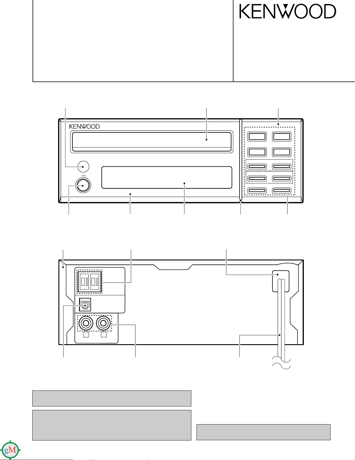
Indicator
(B12-0318-04)
Knob
(K29-6744-04)
Metallic cabinet
(A01-3321-01)
Panel *
(A60-)
Rectangular receptacle
(E08-0312-05)
Panel
(A29-0872-03)
Front glass
(B10-2372-03)
Escutcheon
(B07-2363-04)
Power cord bushing
(J42-0083-05)
Panel *
(A60-)
Knob
(K29-6743-03)
Oscillating module
(W02-1114-05)
Phono jack
(E63-0122-05)
In compliance with Federal Regulations, following are reproductions of
labels on, or inside the product relating to laser product safety.
KENWOOD-Crop. certifies this equipment conforms to DHHS Regulations
No. 21 DFR 1040. 10, Chapter 1, Subchapter J.
DANGER : Laser radiation when open and interlock defeated.
AVOID DIRECT EXPOSURE TO BEAM
AC power cord *
(E30-)
Illustration is DP-SE7Mtype.
* Refer to parts list on page 17.
Refer to DP-SA7 service manual (B51-5243-00) if you require
Disassembly for repair in detail.
DP-SE7/SE7(G)/SE9
CONTENTS / EXTERNAL VIEW
Contents
CONTENTS / EXTERNAL VIEW............................... 2
CIRCUIT DESCRIPTION............................................3
ADJUSTMENT............................................................6
PC BOARD ................................................................ 7
SCHEMATIC DIAGRAM............................................ 9
EXPLODED VIEW ....................................................15
PARTS LIST..............................................................17
SPECIFICATIONS ......................................Back cover
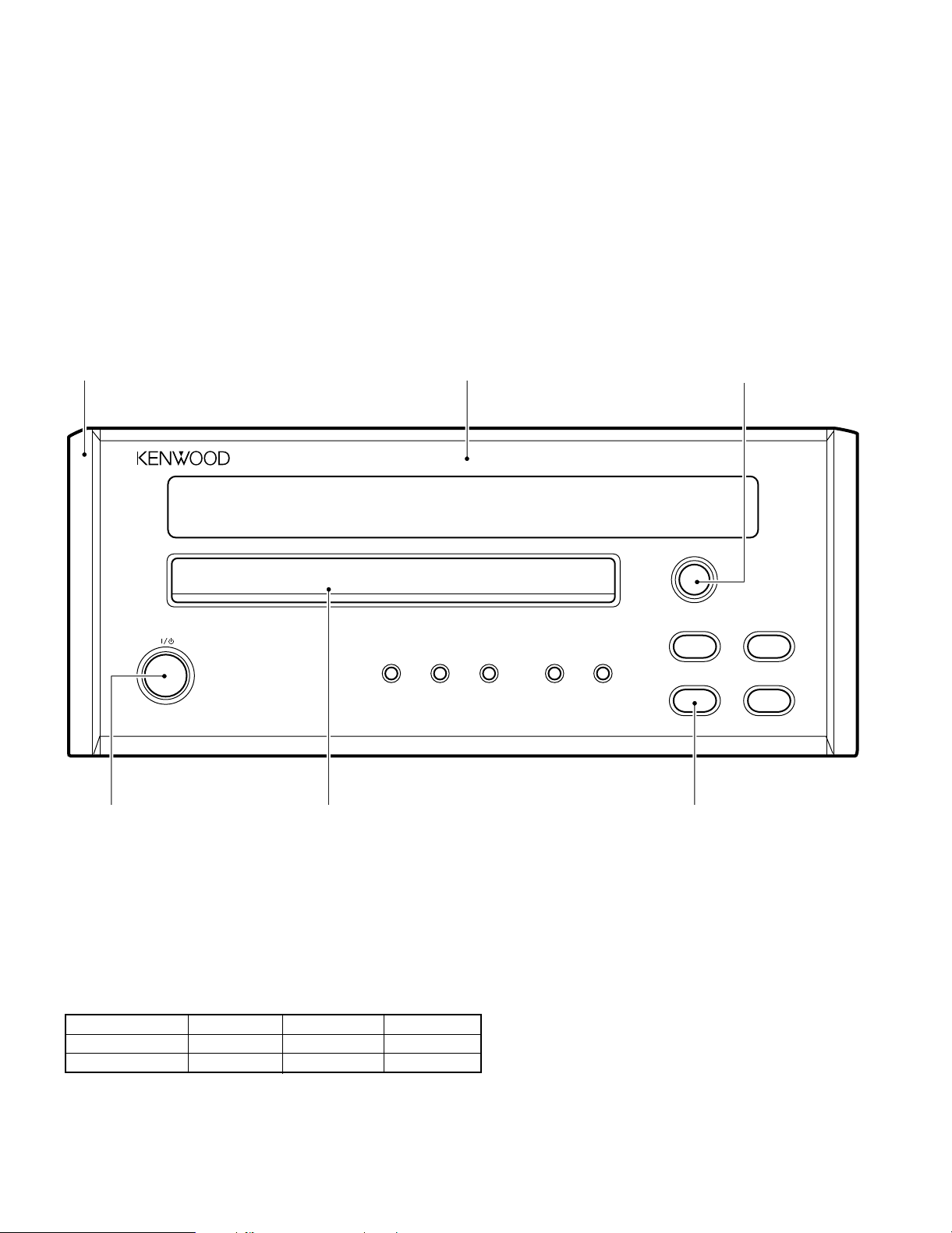
Side plate
(A50-1303-12)
on/standby
compact disc player
Panel
(A60-1266-02)
DP-SE9
'
time space repeat 1 ¡
D.R.I.V.E. with 24 bit D/A conversion
24 bit fine D.R.I.V.E.
Knob
(K29-6742-04)
0
7
4 ¢
6
Knob
(K29-6741-04)
Panel
(A29-0871-03)
System configuration
SYSTEM NAME RECEIVER CD PLAYER SPEAKER
HM-701 R-SE7 DP-SE7 LS-SE7
HM-901 R-SE9 DP-SE9 LS-SE9
2
Knob
(K29-6766-04)
Illustration is DP-SE9.
CIRCUIT DESCRIPTION
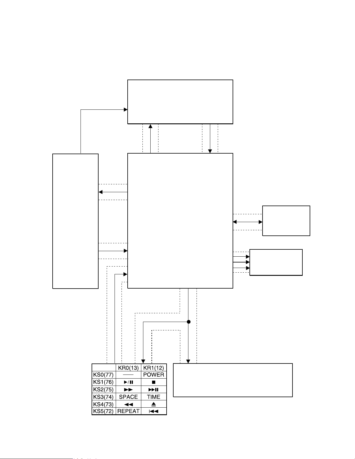
(X32) IC2
KAN03
213BGN
8-BT-207GK
µPD78044FGF
SDATA
SBUSY
(X25) IC5
CLK, DTA, LAT
S. CLK M. ON
MUTE XLON
SENSE
SCOR
SUBQ
(SLTSW)
(FOK , GFS)
SGATE
SCK
SDT
KR0,KR1
SLT SW
Seg key scm pin
KSL-
CD mecha
MOTOR CONTROL
TERMINAL
SWITCH INPUT
X 2
KEY INPUT
X 2
GRID X 8
SEGMENT X 12
SYSTEM
SERIAL
SIGNAL
D.S.P.
CXD 2507AQ
6
KEY MATRIX
1. Microprocessor
1-1. Microprocessor periphery block diagram
DP-SE7/SE7(G)/SE9
3

DP-SE7/SE7(G)/SE9
CIRCUIT DESCRIPTION
1-2 Pin description
(uPD78044FGF-071 : X25, IC4)
PIN No. PIN NAME I/O DESCRIPTION
1~7 Grid 2G~8G O FL Digit control (Grid 2G~8G)
8 Vdd O Power supply (+5)
9 SQCK O Q-data read clock output.
10 STBY O Not use (OPEN)
11 SUBQ I Q-data (or SLT SW) input
12 KR 1 I Key return input 1
13 KR 0 I Key return input 0
14~16 NC I Not use (PULL DOWN)
17 RESET I Reset input
18, 19 NC I Not use (PULL DOWN)
20 AVss – Not use (GND)
21~24 NC I Not use (PULL DOWN)
25 SDT O Enable output to KAN03
26 SCK O Clock output to KAN03
27 S GATE O Data output for KAN03
28 NC I Not use
29 AVdd – Not use (+5V)
30 AVref – Not use (GND)
31 DEFECT I Scratch disk compel sat
32 XT2 – Not use (OPEN)
33 Vss – GND
34 X1 I System clock
35 X2 – System clock
36 RMUTE O Analog mute
37 CLK O CXD2507AQ clock output
38 LATCH O CXD2507AQ latch output
39 DATA O CXD2507AQ data output
40 SENSE I SENSE/GFS/F.OK input
41 D.S O Not use
42 S.DATA I/O Serial DATA I/O
43 S.BUSY I/O Serial BUSY I/O
44 SCOR I Sub-code synch detect
45 NC I Not use (PULL DOWN)
46 M.ON O Focus lock compensation
47 REMOCON I REMOCON
48 Vpp – GND
49 CLOSE SW I Tray close (L : close)
50 OPEN SW I Tray open (L : open)
51 NC I Not use (PULL DOWN)
52 Vdd – Power supply (+5V)
53 OPEN MOTOR O Motor [OPEN] (H : OPEN/T.U.DOWN)
54 CLOSE MOTOR O Motor [CLOSE] (H : CLOSE/T.U.UP)
55~64 NC O Not use (OPEN)
65~70 Sa~Sf O FL Segment (SEG Sa~Sf)
71 Vlord – FL driver power supply (-30V)
72~77 SEG Sg~Sl/KS 5~0 O FL Segment Sg~Sl and key scan (KS5~KS0)
78, 79 NC O Not use (open)
80 GRID 1G O FL digit (Grid 1G)
4
DP-SE7/SE7(G)/SE9
CIRCUIT DESCRIPTION
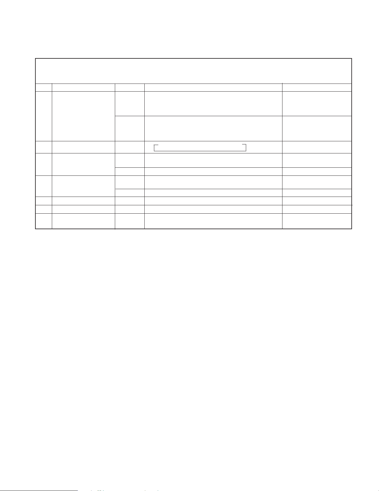
2. Test mode
MODE "0 0" : Use for Test or alignment
Setting the test mode : While pressing the "REPEAT" key, plug the AC cord
into wall output.
No. Key Display Operation Remarks
(1)Focus servo.........................................ON
03 (2) Tracking servo ....................................OFF
1 PLAY/ PAUSE (3) Feed servo .........................................OFF
6 (1) Focus servo.........................................ON
05 (2) Tracking servo.....................................ON
(3) Feed servo..........................................ON
2 UP ¢
3 FB 1
4 FF ¡ 01 Pick manual feed(inside = outside)
5 STOP 7 01 Pick-up initialize
6 OPEN / CLOSE 0 Tray open / close
7 DOWN 4 01
01 Pick manual feed (outside = inside)
05 FB operation is available
05 FF operation is available
All display ON = All display OFF
Cancel the test mode, and
return to normal mode.
TE-adjustment
F-GAIN / T-GAIN
FE-B adjustment
Stop mode only
Time display goes off
Stop mode only
Time display goes off
Play track No.01
5
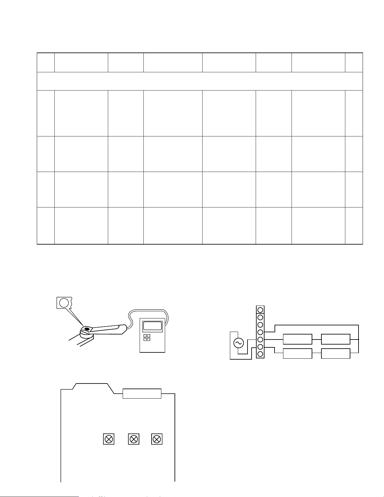
DP-SE7/SE7(G)/SE9
ADJUSTMENT
No. ITEM
While pressing the "REPEAT" key, turn the AC ON.
{ Refer to test mode (MODE 0 0) }
1 LASER POWER
FOCUS ERROR
2
3
Note:
Type 4 disc : SONY YEDS-18 Test Disc or equivalent.(KTD-0
LPF: Around 47 kΩ+ 390 pF or so.
Step 1~4 are in Test Mode.
BIAS
TRACKING ERROR
BALANCE
INPUT
SETTINGS
−
Test disc
Type 4
Test disc
Type 4
Test disc
Type 4
Apply signal of
1.2 kHz,
50mVrms to
CN3 pin 5-6.
OUTPUT
SETTINGS
Apply the sensor section
of optical power meter
on the pickup lens.
Connect an oscilloscope
as follows.
CH1 : RF (CN3 pin 1)
CH2 : TE (CN3 pin 6)
Connect an oscilloscope
as follows.
CH1 : RF (CN3 pin 1)
CH2 : TE (CN3 pin 6)
Connect a LPF to CN3
pin 5-6 to which you
connect an oscilloscope
or AC voltmeters.
✽)
PLAYER
SETTINGS
Press the
PLAY/PAUSE key,
then confirm that the
LED is "03".
Press the
/PAUSE
PLAY
then confirm that the
LED is "05".
Press the
PLAY/PAUSE key,
then confirm that the
LED
Press the
PLAY/PAUSE key,
then confirm that the
LED
key,
is "03".
is "05".
ALIGNMENT
POINTS
−
FE BIAS
VR2
TE BALANCE
VR1
TRACKING
GAIN
VR3
ALIGN
FOR
On the power from
0.08 to 0.15 mW,
when the diffraction
grating is correctly
aligned with the RF
level of 0.6 Vp-p or
more.
Optimum eye pattern
Symmetry between
upper and lower
patterns
Two VTVMs should
read the same value.
FIG.
(a)
(e)4 TRACKING GAIN
Pickup
ALIGNMENT POINTS
T-GAIN
VR3 VR1 VR2
0.08 ~ 0.15 mW
Optical power meter
CN1
TE-B FE-B
(e)Tracking gainn(a)Laser power
1.2 kHz
50 mVrms
CN3
1
RF
2
FE1
FE2
3
_
+
VC
4
TE2
5
TE1
6
7
S.S
L.P.F.
L.P.F.
VC
+
VTVM
+
VTVM
6
 Loading...