

Page 1
Model 2015
THD Multimeter
Service Manual
SHIFT
LOCAL
POWER
SCAN
STEP CH2 CH3 CH4 CH5 CH6 CH7 CH8 CH9 CH10
TALK
LSTN
SRQ
SHIFT
TIMER
MATH
DCV
EX TRIG
SAVE SETUP
SOURCE
CH1REM
HOLD TRIG FAST MED SLOW AUTO ERR
THD
ACV
HOLD
TRIG
MEAS
THD
dBm
DCI
LIMITS ON/OFFDELAY
STORE
RECALL
CONFIG HALT
STEP SCAN
dB
ACI
REL FILT
CONT
Ω2 Ω4
TEST
GPIB
DIGITS RATE
Contains Servicing Information
CAL
RELFILTER
RS232
MATH
REAR
4W
BUFFER
STAT
2015 THD MULTIMETER
PERIOD TCOUPL
FREQ
TEMP
EXIT ENTER
RANGE
AUTO
RANGE
Ω 4 WIRE
350V
PEAK
F
FRONT/REAR
SENSE
INPUTS
INPUT
HI
1000V
!
PEAK
LO
500V
PEAK
R
3A 250V
AMPS
Page 2

W ARRANTY
Keithley Instruments, Inc. warrants this product to be free from defects in material and workmanship for a
period of 3 years from date of shipment.
Keithley Instruments, Inc. warrants the following items for 90 days from the date of shipment: probes,
cables, rechargeable batteries, diskettes, and documentation.
During the warranty period, we will, at our option, either repair or replace any product that proves to be
defective.
T o e xercise this w arranty, write or call your local Keithle y representati v e, or contact K eithle y headquarters in
Cleveland, Ohio. You will be given prompt assistance and return instructions. Send the product, transportation prepaid, to the indicated service facility. Repairs will be made and the product returned, transportation
prepaid. Repaired or replaced products are warranted for the balance of the original warranty period, or at
least 90 days.
LIMIT A TION OF W ARRANTY
This warranty does not apply to defects resulting from product modification without Keithley’s express written consent, or misuse of any product or part. This warranty also does not apply to fuses, software, nonrechargeable batteries, damage from battery leakage, or problems arising from normal wear or failure to follow instructions.
THIS WARRANTY IS IN LIEU OF ALL OTHER WARRANTIES, EXPRESSED OR IMPLIED,
INCLUDING ANY IMPLIED WARRANTY OF MERCHANTABILITY OR FITNESS FOR A PARTICULAR USE. THE REMEDIES PROVIDED HEREIN ARE BUYER’S SOLE AND EXCLUSIVE REMEDIES.
NEITHER KEITHLEY INSTRUMENTS, INC. NOR ANY OF ITS EMPLOYEES SHALL BE LIABLE
FOR ANY DIRECT, INDIRECT, SPECIAL, INCIDENTAL OR CONSEQUENTIAL DAMAGES ARISING OUT OF THE USE OF ITS INSTRUMENTS AND SOFTWARE EVEN IF KEITHLEY INSTRUMENTS, INC., HAS BEEN ADVISED IN ADVANCE OF THE POSSIBILITY OF SUCH DAMAGES.
SUCH EXCLUDED DAMAGES SHALL INCLUDE, BUT ARE NOT LIMITED TO: COSTS OF
REMOVAL AND INSTALLATION, LOSSES SUSTAINED AS THE RESULT OF INJURY TO ANY PERSON, OR DAMAGE TO PROPERTY.
1/99
Page 3

Model 2015 THD Multimeter
Service Manual
©1998, Keithley Instruments, Inc.
All rights reserved.
Cleveland, Ohio, U.S.A.
Third Printing, June 1999
Document Number: 2015-902-01 Rev. C
Page 4

Manual Print History
The print history shown below lists the printing dates of all Revisions and Addenda created
for this manual. The Revision Le vel letter increases alphabetically as the manual under goes subsequent updates. Addenda, which are released between Revisions, contain important change information that the user should incorporate immediately into the manual. Addenda are numbered
sequentially. When a new Re vision is created, all Addenda associated with the previous Re vision
of the manual are incorporated into the new Revision of the manual. Each ne w Revision includes
a revised copy of this print history page.
Revision A (Document Number 2015-902-01).................................................................May 1998
Revision B (Document Number 2015-902-01)..................................................................July 1998
Revision C (Document Number 2015-902-01)................................................................. June 1999
All Keithley product names are trademarks or registered trademarks of Keithley Instruments, Inc.
Other brand names are trademarks or registered trademarks of their respective holders.
Page 5

Safety Precautions
The following safety precautions should be observed before using this product and any associated instrumentation. Although some instruments and accessories would normally be used with non-hazardous v oltages, there
are situations where hazardous conditions may be present.
This product is intended for use by qualified personnel who recognize shock hazards and are familiar with the
safety precautions required to avoid possible injury. Read the operating information carefully before using the
product.
The types of product users are:
Responsible body is the individual or group responsible for the use and maintenance of equipment, for ensuring
that the equipment is operated within its specifications and operating limits, and for ensuring that operators are
adequately trained.
Operators use the product for its intended function. They must be trained in electrical safety procedures and
proper use of the instrument. They must be protected from electric shock and contact with hazardous live circuits.
Maintenance personnel perform routine procedures on the product to keep it operating, for example, setting
the line voltage or replacing consumable materials. Maintenance procedures are described in the manual. The
procedures explicitly state if the operator may perform them. Otherwise, they should be performed only by service personnel.
Service personnel are trained to work on live circuits, and perform safe installations and repairs of products.
Only properly trained service personnel may perform installation and service procedures.
Exercise extreme caution when a shock hazard is present. Lethal voltage may be present on cable connector
jacks or test fixtures. The American National Standards Institute (ANSI) states that a shock hazard e xists when
voltage levels greater than 30V RMS, 42.4V peak, or 60VDC are present. A good safety practice is to expect
that hazardous voltage is present in any unknown circuit before measuring.
Users of this product must be protected from electric shock at all times. The responsible body must ensure that
users are prevented access and/or insulated from every connection point. In some cases, connections must be
exposed to potential human contact. Product users in these circumstances must be trained to protect themselves
from the risk of electric shock. If the circuit is capable of operating at or above 1000 volts, no conductive part
of the circuit may be exposed.
As described in the International Electrotechnical Commission (IEC) Standard IEC 664, digital multimeter
measuring circuits (e.g., Keithley Models 175A, 199, 2000, 2001, 2002, and 2010) are Installation Category II.
All other instruments’ signal terminals are Installation Category I and must not be connected to mains.
Do not connect switching cards directly to unlimited power circuits. They are intended to be used with impedance limited sources. NEVER connect switching cards directly to AC mains. When connecting sources to
switching cards, install protective devices to limit fault current and voltage to the card.
Before operating an instrument, make sure the line cord is connected to a properly grounded power receptacle.
Inspect the connecting cables, test leads, and jumpers for possible wear, cracks, or breaks before each use.
For maximum safety, do not touch the product, test cables, or any other instruments while power is applied to
the circuit under test. ALWAYS remove power from the entire test system and discharge an y capacitors before:
connecting or disconnecting cables or jumpers, installing or removing switching cards, or making internal
changes, such as installing or removing jumpers.
Do not touch any object that could provide a current path to the common side of the circuit under test or power
line (earth) ground. Always make measurements with dry hands while standing on a dry, insulated surface capable of withstanding the voltage being measured.
Page 6

The instrument and accessories must be used in accordance with its specifications and operating instructions or
the safety of the equipment may be impaired.
Do not exceed the maximum signal levels of the instruments and accessories, as defined in the specifications
and operating information, and as shown on the instrument or test fixture panels, or switching card.
When fuses are used in a product, replace with same type and rating for continued protection against fire hazard.
Chassis connections must only be used as shield connections for measuring circuits, NOT as safety earth ground
connections.
If you are using a test fixture, keep the lid closed while power is applied to the device under test. Safe operation
requires the use of a lid interlock.
If a screw is present, connect it to safety earth ground using the wire recommended in the user documentation.
!
The symbol on an instrument indicates that the user should refer to the operating instructions located in
the manual.
The symbol on an instrument shows that it can source or measure 1000 volts or more, including the combined effect of normal and common mode voltages. Use standard safety precautions to avoid personal contact
with these voltages.
The WARNING heading in a manual explains dangers that might result in personal injury or death. Always
read the associated information very carefully before performing the indicated procedure.
The CAUTION heading in a manual explains hazards that could damage the instrument. Such damage may
invalidate the warranty.
Instrumentation and accessories shall not be connected to humans.
Before performing any maintenance, disconnect the line cord and all test cables.
To maintain protection from electric shock and fire, replacement components in mains circuits, including the
power transformer, test leads, and input jacks, must be purchased from Keithley Instruments. Standard fuses,
with applicable national safety approvals, may be used if the rating and type are the same. Other components
that are not safety related may be purchased from other suppliers as long as they are equivalent to the original
component. (Note that selected parts should be purchased only through Keithley Instruments to maintain accuracy and functionality of the product.) If you are unsure about the applicability of a replacement component,
call a Keithley Instruments office for information.
T o clean an instrument, use a damp cloth or mild, water based cleaner . Clean the e xterior of the instrument only .
Do not apply cleaner directly to the instrument or allow liquids to enter or spill on the instrument. Products that
consist of a circuit board with no case or chassis (e.g., data acquisition board for installation into a computer)
should never require cleaning if handled according to instructions. If the board becomes contaminated and operation is affected, the board should be returned to the factory for proper cleaning/servicing.
Rev. 2/99
Page 7

T able of Contents
1
Performance Verification
Introduction ........................................................................................ 1-2
Verification test requirements ............................................................ 1-3
Environmental conditions .............................................................. 1-3
Warm-up period ............................................................................. 1-3
Line power ..................................................................................... 1-3
Recommended test equipment ........................................................... 1-4
Verification limits ............................................................................... 1-5
Example reading limit calculation ................................................. 1-5
Calculating resistance reading limits ............................................. 1-5
Restoring factory defaults .................................................................. 1-6
Performing the verification test procedures ....................................... 1-7
Test summary ................................................................................. 1-7
Test considerations ......................................................................... 1-7
Verifying DC voltage ......................................................................... 1-8
Verifying AC voltage ....................................................................... 1-10
Verifying DC current ....................................................................... 1-12
Verifying AC current ........................................................................ 1-13
Verifying resistance ......................................................................... 1-14
Verifying temperature ...................................................................... 1-16
Verifying frequency ......................................................................... 1-17
Verifying total harmonic distortion .................................................. 1-18
Verifying function generator amplitude ........................................... 1-19
2
Calibration
Introduction ........................................................................................ 2-2
Environmental conditions .................................................................. 2-3
Warm-up period ............................................................................. 2-3
Line power ..................................................................................... 2-3
Calibration considerations ................................................................. 2-4
Calibration code ................................................................................. 2-5
Front panel calibration code ........................................................... 2-5
Remote calibration code ................................................................. 2-5
Comprehensive calibration ................................................................ 2-6
Calibration cycle ............................................................................ 2-6
Recommended equipment .............................................................. 2-6
Aborting calibration ....................................................................... 2-7
Front panel calibration ................................................................... 2-7
Preparing the Model 2015 for calibration ...................................... 2-7
Front panel short and open calibration ........................................... 2-8
DC volts calibration ....................................................................... 2-9
Page 8

Resistance calibration .................................................................. 2-11
DC current calibration ................................................................. 2-12
AC voltage calibration ................................................................. 2-13
AC current calibration ................................................................. 2-14
Distortion calibration ................................................................... 2-14
Function generator calibration ..................................................... 2-15
Setting calibration dates and saving calibration .......................... 2-16
Remote calibration ....................................................................... 2-16
Preparing the Model 2015 for calibration .................................... 2-17
Short and open calibration ........................................................... 2-17
DC volts calibration ..................................................................... 2-18
Resistance calibration .................................................................. 2-19
DC current calibration ................................................................. 2-20
AC voltage calibration ................................................................. 2-21
AC current calibration ................................................................. 2-22
Distortion calibration ................................................................... 2-22
Function generator calibration ..................................................... 2-23
Programming calibration dates .................................................... 2-23
Saving calibration constants ........................................................ 2-23
Locking out calibration ................................................................ 2-23
Manufacturing calibration ............................................................... 2-24
Recommended test equipment ..................................................... 2-24
Unlocking manufacturing calibration .......................................... 2-24
Measuring synthesizer signal amplitude ...................................... 2-24
Front panel manufacturing calibration ......................................... 2-25
Remote manufacturing calibration .............................................. 2-26
3
Routine Maintenance
Introduction ....................................................................................... 3-2
Setting the line voltage and replacing the line fuse ....................... 3-2
Replacing the AMPS fuse .............................................................. 3-3
4
T roubleshooting
Introduction ....................................................................................... 4-2
Repair considerations ........................................................................ 4-3
Power-on self-test .............................................................................. 4-4
Front panel tests ................................................................................ 4-5
KEY test ......................................................................................... 4-5
DISP test ........................................................................................ 4-5
Principles of operation ...................................................................... 4-6
Power supply ................................................................................. 4-6
Display board ................................................................................. 4-8
Digital circuitry .............................................................................. 4-9
Page 9

Analog circuitry ........................................................................... 4-11
Distortion digital circuitry ............................................................ 4-13
Distortion analog circuitry ........................................................... 4-15
Sine generator circuitry ................................................................ 4-16
Troubleshooting ............................................................................... 4-18
Display board checks ................................................................... 4-18
Power supply checks .................................................................... 4-19
Digital circuitry checks ................................................................ 4-20
Analog signal switching states ..................................................... 4-21
Disassembly
5
Introduction ........................................................................................ 5-2
Handling and cleaning ....................................................................... 5-3
Handling PC boards ....................................................................... 5-3
Solder repairs ................................................................................. 5-3
Static sensitive devices ................................................................... 5-4
Assembly drawings ............................................................................ 5-5
Disassembly procedures .................................................................... 5-6
Case cover removal ........................................................................ 5-6
DMM board removal ...................................................................... 5-6
DSP board removal ........................................................................ 5-7
Front panel disassembly ................................................................. 5-8
Removing power components ........................................................ 5-8
Instrument reassembly ....................................................................... 5-9
Input terminal wire connections ..................................................... 5-9
Power module wire connections .................................................... 5-9
Changing trigger link lines .............................................................. 5-10
Main CPU firmware replacement .................................................... 5-11
6
Replaceable Parts
Introduction ........................................................................................ 6-2
Parts lists ............................................................................................ 6-2
Ordering information ......................................................................... 6-2
Factory service ................................................................................... 6-2
Component layouts ............................................................................ 6-2
A
Specifications
Accuracy calculations ....................................................................... A-9
Calculating DC characteristics accuracy ....................................... A-9
Calculating AC characteristics accuracy ....................................... A-9
Calculating dBm characteristics accuracy .................................. A-10
Calculating dB characteristics accuracy ...................................... A-10
Distortion characteristics ............................................................. A-11
Page 10

Calculating generator amplitude accuracy .................................. A-12
Additional derating factors ......................................................... A-12
Optimizing measurement accuracy ................................................ A-13
DC voltage, DC current, and resistance ...................................... A-13
AC voltage and AC current ......................................................... A-13
Temperature ................................................................................ A-13
Optimizing measurement speed ..................................................... A-14
DC voltage, DC current, and resistance ...................................... A-14
AC voltage and AC current ......................................................... A-14
Temperature ................................................................................ A-14
B
Calibration Reference
Introduction ...................................................................................... B-2
Command summary ......................................................................... B-3
Miscellaneous calibration commands .............................................. B-5
:CODE .......................................................................................... B-5
:COUNt? ....................................................................................... B-5
:INIT ............................................................................................. B-6
:LOCK .......................................................................................... B-6
:LOCK? ........................................................................................ B-7
:SAVE ........................................................................................... B-7
:DATE ........................................................................................... B-8
:NDUE .......................................................................................... B-8
DC calibration commands ................................................................ B-9
:STEP1 .......................................................................................... B-9
:STEP2 ........................................................................................ B-10
:STEP3 ........................................................................................ B-10
:STEP4 ........................................................................................ B-10
:STEP5 ........................................................................................ B-11
:STEP6 ........................................................................................ B-11
:STEP7 ........................................................................................ B-11
:STEP8 ........................................................................................ B-12
:STEP9 ........................................................................................ B-12
:STEP10 ...................................................................................... B-12
:STEP11 ...................................................................................... B-13
:STEP12 ...................................................................................... B-13
AC calibration commands .............................................................. B-14
:AC:STEP<n> ............................................................................. B-15
Distortion and function generator calibration commands ............. B-16
:DIST:STEP1 .............................................................................. B-16
:DIST:STEP2 .............................................................................. B-16
:FGEN:STEP1 ............................................................................ B-16
Page 11

Manufacturing calibration commands ............................................ B-17
:AC:STEP<14|15> ...................................................................... B-17
:DC:STEP0 .................................................................................. B-17
Remote error reporting ................................................................... B-18
Error summary ............................................................................ B-18
Error queue .................................................................................. B-20
Status byte EAV (Error Available) bit ......................................... B-20
Generating an SRQ on error ........................................................ B-20
Detecting calibration step completion ............................................ B-21
Using the *OPC? query ............................................................... B-21
Using the *OPC command .......................................................... B-21
Generating an SRQ on calibration complete ............................... B-22
Calibration Program
C
Introduction ....................................................................................... C-2
Computer hardware requirements ..................................................... C-2
Software requirements ...................................................................... C-2
Calibration equipment ...................................................................... C-2
General program instructions ........................................................... C-3
Page 12

List of Illustrations
1
Performance Verification
Connections for DC volts verification .............................................. 1-8
Connections for AC volts verification ............................................. 1-10
Connections for DC current verification ......................................... 1-12
Connections for AC current verification ......................................... 1-13
Connections for resistance verification (100 Ω -10M Ω range) ........ 1-14
Connections for resistance verification (100M Ω range) ................. 1-15
Connections for frequency verification ........................................... 1-17
Connections for total harmonic distortion verification ................... 1-18
Connections for function generator amplitude verification ............ 1-19
2
Calibration
Low-thermal short connections ......................................................... 2-8
Connections for DC volts and ohms calibration ............................... 2-9
Connections for DC and AC amps calibration ................................ 2-12
Connections for AC volts calibration .............................................. 2-13
Connections for distortion calibration ............................................. 2-15
Connections for function generator calibration ............................... 2-15
Synthesizer connections for manufacturing calibration .................. 2-25
Routine Maintenance
3
Power module .................................................................................... 3-3
T roubleshooting
4
Power supply block diagram ............................................................. 4-6
Digital circuitry block diagram ......................................................... 4-8
Analog circuitry block diagram ....................................................... 4-11
Distortion digital circuitry block diagram ....................................... 4-13
Distortion analog circuitry block diagram ...................................... 4-15
Sine generator circuitry block diagram ........................................... 4-16
5
Disassembly
Trigger link line connections ........................................................... 5-10
Page 13

List of T ables
1
Performance Verification
Recommended verification equipment ........................................... 1-4
DCV reading limits ........................................................................ 1-9
ACV reading limits ....................................................................... 1-11
DCI limits ..................................................................................... 1-12
ACI limits ..................................................................................... 1-13
Limits for resistance verification .................................................. 1-15
Thermocouple temperature verification reading limits ................ 1-16
Calibration
2
Recommended equipment for comprehensive calibration ............. 2-6
Comprehensive calibration procedures .......................................... 2-8
DC volts calibration summary ...................................................... 2-10
Ohms calibration summary .......................................................... 2-11
DC current calibration summary .................................................. 2-12
AC voltage calibration summary .................................................. 2-13
AC current calibration summary .................................................. 2-14
Distortion and function generator calibration summary .............. 2-15
DC voltage calibration programming steps .................................. 2-18
Resistance calibration programming steps ................................... 2-19
DC current calibration programming steps .................................. 2-20
AC voltage calibration programming steps .................................. 2-21
AC current calibration programming steps .................................. 2-22
Distortion and function generator calibration steps ..................... 2-22
Recommended equipment for manufacturing calibration ............ 2-24
Ω
Ω
Ω 2/ Ω
Routine Maintenance
3
Power line fuse ............................................................................... 3-3
T roubleshooting
4
Power supply components .............................................................. 4-7
Display board checks ................................................................... 4-18
Power supply checks .................................................................... 4-19
Digital circuitry checks ................................................................ 4-20
DCV signal switching .................................................................. 4-21
ACV and FREQ signal switching ................................................. 4-21
2 signal switching ...................................................................... 4-22
4 signal switching ...................................................................... 4-22
4 reference switching .......................................................... 4-22
DCA signal switching .................................................................. 4-23
Page 14

ACA signal switching .................................................................. 4-23
DCV signal multiplexing and gain .............................................. 4-23
ACV and ACA signal multiplexing and gain ............................... 4-23
DCA signal multiplexing and gain .............................................. 4-24
2 signal multiplexing and gain .................................................. 4-24
4 signal multiplexing and gain .................................................. 4-24
Switching device locations ............................................................ 4-25
5
Disassembly
Input terminal wire colors .............................................................. 5-9
Power module wire colors .............................................................. 5-9
6
Replaceable Parts
DMM (mother) board parts list ...................................................... 6-3
Display board parts list .................................................................. 6-9
Distortion (DSP) board parts list .................................................. 6-10
Mechanical parts list .................................................................... 6-14
Ω
Ω
B
Calibration Reference
Remote calibration command summary ....................................... B-3
DC calibration commands ............................................................. B-9
AC calibration commands ........................................................... B-14
Distortion and function generator calibration commands ........... B-16
Calibration error summary .......................................................... B-18
Page 15

1
Performance
V erification
Page 16

1-2 Performance Verification
Introduction
the limits stated in the instrument’s one-year accurac y specifications. Y ou can perform these ver ification procedures:
WARNING The information in this section is intended only for qualified service per-
Use the procedures in this section to verify that Model 2015 Multimeter accuracy is within
• When you first receive the instrument to make sure that it w as not damaged during shipment, and that the unit meets factory specifications.
• If the instrument’s accuracy is questionable.
• Following calibration.
sonnel. Do not attempt these procedures unless you are qualified to do so.
NOTE If the instrument is still under warranty and its performance is outside specified
limits, contact your Keithley representative or the factory to determine the correct
course of action.
Page 17

Performance Verification 1-3
V erification test requirements
Be sure that you perform the verification tests:
• Under the proper environmental conditions.
• After the specified warm-up period.
• Using the correct line voltage.
• Using the proper calibration equipment.
• Using the specified reading limits.
Environmental conditions
Conduct your performance verification procedures in a test environment that has:
• An ambient temperature of 18˚ to 28°C (65˚ to 82°F).
• A relative humidity of less than 80% unless otherwise noted.
W arm-up period
Allow the Model 2015 Multimeter to warm up for at least one hour before conducting the v er-
ification procedures.
If the instrument has been subjected to temperature extremes (those outside the ranges stated
above), allow additional time for the instrument’s internal temperature to stabilize. Typically,
allow one extra hour to stabilize a unit that is 10°C (18°F) outside the specified temperature
range.
Also, allow the test equipment to warm up for the minimum time specified by the
manufacturer.
Line power
The Model 2015 Multimeter requires a line voltage of 100V/120V/220V/240V, ±10% and a
line frequency of 45Hz to 66Hz and 360Hz to 440Hz.
Page 18

Ω
Ω
Ω
1-4 Performance Verification
Recommended test equipment
T able 1-1 summarizes recommended verification equipment. You can use alternate equipment
as long as that equipment has specifications at least as good as those listed in Table 1-1. Keep in
mind, however, that the calibrator will add to the uncertainty of each measurement.
Table 1-1
Recommended verification equipment
Fluke 5700A Calibrator:
AC voltage
DC voltage
100mV:±14ppm
1.0V:±7ppm
10V:±5ppm
100V:±7ppm
1000V:±9ppm
Fluke 5725A Amplifier:
AC Voltage, 50kHz: 700V, ±375ppm
Keithley 3930A or 3940 Frequency Synthesizer:
1V RMS, 1kHz, ±5ppm
Stanford Research Systems DS-360 Ultra Low Distortion Function Generator:
1kHz, .0.95V RMS sine wave, -100dB THD
Miscellaneous Equipment:
Double banana plug to double banana plug shielded cable
BNC to double banana plug shielded cable
(1kHz, 50kHz) DC current
100mV:±200ppm
1.0V:±82ppm
10V:±82ppm
100V:±90ppm
700V:±85ppm
10mA:±60ppm
100mA:±70ppm
1A:±110ppm
2.2A:±94ppm
AC current
(1kHZ) Resistance
1A:±690ppm
2.2A:±682ppm
100
:±17ppm
1k
:±12ppm
10k
:±11ppm
100k Ω :±13ppm
1M Ω :±18ppm
10M Ω :±37ppm
100M Ω :±120ppm
NOTE: The Fluke 5725A amplifier is necessary only if you wish to verify the 750V AC range at 50kHz.
Verification at 220V, 50kHz using only the 5700A calibrator is adequate for most applications.
Page 19

×
V erification limits
The verification limits stated in this section have been calculated using only the Model 2015
one-year accuracy specifications, and they do not include test equipment uncertainty. If a particular measurement falls slightly outside the allowable range, recalculate new limits based on
both Model 2015 specifications and pertinent calibration equipment specifications.
Example reading limit calculation
The following is an example of how reading limits have been calculated:
Assume you are testing the 10V DC range using a 10V input value. Using the Model 2015
one-year accuracy specification for 10V DC of ± (30ppm of reading + 5ppm of range), the calculated limits are:
Performance Verification 1-5
Reading limits = 10V ± [(10V
Reading limits = 10V ± (.0003 + .00005)
Reading limits = 10V ± .00035V
Reading limits = 9.99965V to 10.00035V
30ppm) + (10V × 5ppm)]
Calculating resistance reading limits
Resistance reading limits must be recalculated based on the actual calibration resistance values supplied by the equipment manufacturer . Calculations are performed in the same manner as
shown in the preceding example, except, of course, that you should use the actual calibration
resistance values instead of the nominal values when performing your calculations.
Page 20

1-6 Performance Verification
Restoring factory defaults
Before performing the verification procedures, restore the instrument to its factory defaults
as follows:
1. Press
2. Using either range key , select FACT , then restore the factory def ault conditions by press-
3. Factory defaults will be set as follows:
SHIFT and then SETUP . The instrument will display the following prompt:
RESTORE: FACT.
ing
ENTER .
Speed: medium
Filter: 10 readings
Page 21

Performance Verification 1-7
Performing the verification test procedures
T est summary
Verification test procedures include:
• DC volts
• AC volts
• DC current
• AC current
• Resistance
• Temperature
• Frequency
• Total harmonic distortion
• Function generator amplitude
If the Model 2015 is not within specifications and not under warranty , see the calibration procedures in Section 2.
T est considerations
When performing the verification procedures:
• Be sure to restore factory defaults as outlined above.
• After restoring factory defaults and selecting the measuring function, select the SLOW
integration rate with the RATE key.
• Make sure that the equipment is properly warmed up and connected to the front panel
input jacks. Also mak e sure that the front panel input jacks are selected with the INPUTS
switch.
• Do not use autoranging for any verification tests because autorange hysteresis may cause
the Model 2015 to be on an incorrect range. For each test signal, you must manually set
the correct range for the Model 2015 using the range keys.
• Make sure the calibrator is in operate before you verify each measurement.
• Always let the source signal settle before taking a reading.
• Do not connect test equipment to the Model 2015 through a scanner or other switching
equipment.
WARNING The maximum common-mode voltage (voltage between INPUT LO and
chassis ground) is 500V peak. Exceeding this value may cause a breakdown
in insulation, creating a shock hazard. Some of the procedures in this section may expose you to dangerous voltages. Use standard safety precautions when such dangerous voltages are encountered to avoid personal
injury caused by electric shock.
Page 22
1-8 Performance Verification
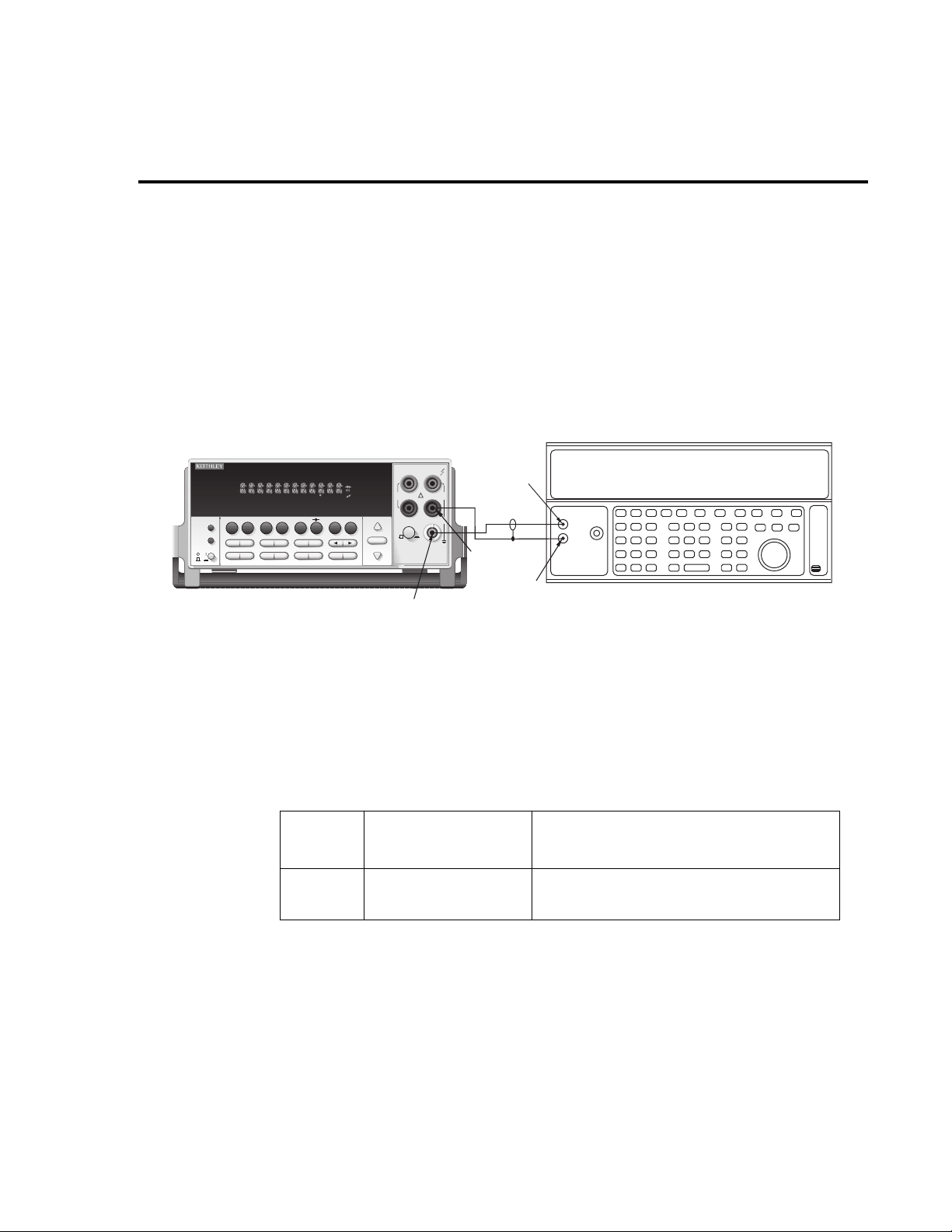
V erifying DC voltage
Check DC voltage accuracy by applying accurate v oltages from the DC v oltage calibrator to
the Model 2015 INPUT jacks and verifying that the displayed readings fall within specified
limits.
CAUTION Do not exceed 1100V peak between INPUT HI and INPUT LO because
instrument damage may occur.
Follow these steps to verify DC voltage accuracy:
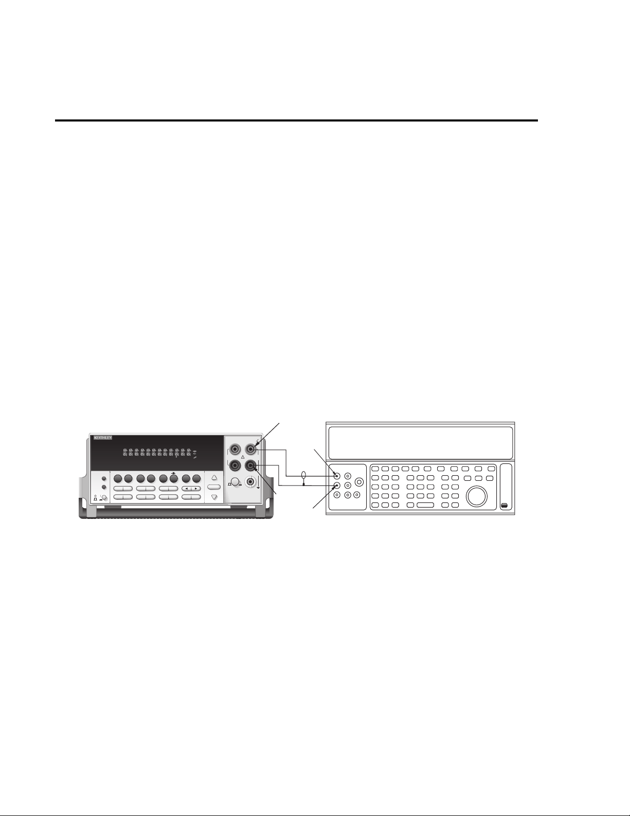
1. Connect the Model 2015 HI and LO INPUT jacks to the DC voltage calibrator as sho wn
in Figure 1-1.
NOTE Use shielded, low-thermal connections when testing the 100mV and 1V ranges to
avoid errors caused by noise or thermal ef fects. Connect the shield to the calibrator’ s
output LO terminal.
Figure 1-1
Connections for DC volts verification
Model 2015
LOCAL
POWER
TALK
LSTN
SRQ
SHIFT
TIMER
MATH
SHIFT
DCV
EX TRIG
SAVE SETUP
SOURCE
THD
SCAN
CH1REM
STEP CH2 CH3 CH4 CH5 CH6 CH7 CH8 CH9 CH10
HOLD TRIG FAST MED SLOW AUTO ERR
REL FILT
dBm
dB
DCI
LIMITS ON/OFFDELAY
STORE
CONFIG HALT
STEP SCAN
RECALL
CONT
ACI
DIGITS RATE
THD
ACV
HOLD
TRIG
MEAS
Ω2 Ω4
TEST
GPIB
CAL
RELFILTER
RS232
MATH
REAR
4W
BUFFER
STAT
2015 THD MULTIMETER
PERIOD TCOUPL
FREQ
TEMP
EXIT ENTER
RANGE
RANGE
AUTO
350V
PEAK
SENSE
Ω 4 WIRE
INPUTS
F
FRONT/REAR
Input HI
INPUT
HI
!
LO
R
3A 250V
AMPS
1000V
PEAK
500V
PEAK
Output HI
Input
DC Voltage Calibrator
LO
Output
LO
Note: Use shielded, low-thermal cables
for 100mV and 1V ranges.
Page 23

Performance Verification 1-9
2. Select the DC volts function by pressing the DCV key, and set the Model 2015 to the
100mV range. Select the SLOW integration rate with the RATE key.
3. Set the calibrator output to 0.00000mV DC, and allow the reading to settle.
4. Enable the Model 2015 REL mode. Leave REL enabled for the remainder of the DC
volts verification tests.
5. Source positive and negative and full-scale voltages for each of the ranges listed in
Table 1-2. For each voltage setting, be sure that the reading is within stated limits.
Table 1-2
DCV reading limits
Range Applied DC voltage* Reading limits (1 year, 18°-28°C)
100mV
1V
10V
100V
1000V
* Source positive and negative values for each range.
100.0000mV
1.000000V
10.00000V
100.0000V
1000.000V
99.9915 to 100.0085mV
0.999963 to 1.000037V
9.99965 to 10.00035V
99.9949 to 100.0051V
999.949 to 1000.051V
Page 24
1-10 Performance Verification
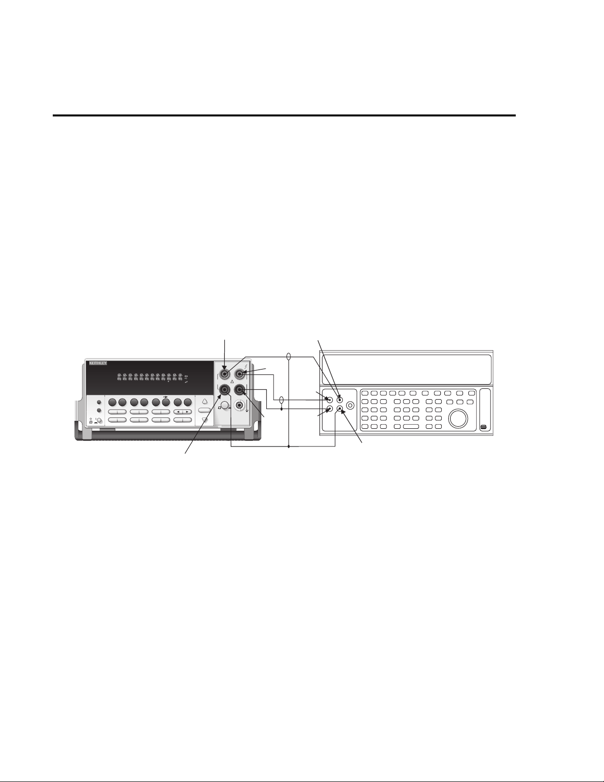
V erifying AC voltage
Check AC voltage accuracy by applying accurate AC voltages at specific frequencies from
the A C v oltage calibrator to the Model 2015 inputs and verifying that the displayed readings f all
within specified ranges.
CAUTION Do not exceed 1100 V peak between INPUT HI and INPUT LO, or 8 × 10
V•Hz input, because instrument damage may occur.
Follow these steps to verify AC voltage accuracy:
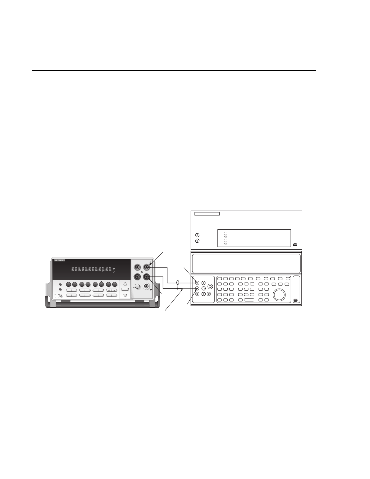
1. Connect the Model 2015 HI and LO INPUT jacks to the A C voltage calibrator as sho wn
in Figure 1-2.
7
Figure 1-2
Connections for AC volts verification
Note: Amplifier required only
for 700V, 50kHz output.
Model 2015
LOCAL
POWER
TALK
LSTN
SRQ
SHIFT
TIMER
MATH
SHIFT
DCV
EX TRIG
SAVE SETUP
SOURCE
THD
SCAN
CH1REM
STEP CH2 CH3 CH4 CH5 CH6 CH7 CH8 CH9 CH10
REL FILT
HOLD TRIG FAST MED SLOW AUTO ERR
dBm
dB
DCI
LIMITS ON/OFFDELAY
STORE
CONFIG HALT
STEP SCAN
RECALL
CONT
ACI
Ω2 Ω4
TEST
GPIB
DIGITS RATE
THD
ACV
HOLD
TRIG
MEAS
RELFILTER
RS232
CAL
BUFFER
STAT
2015 THD MULTIMETER
PERIOD TCOUPL
FREQ
EXIT ENTER
MATH
REAR
4W
TEMP
RANGE
AUTO
RANGE
SENSE
INPUT
Ω 4 WIRE
HI
350V
1000V
!
PEAK
PEAK
LO
500V
PEAK
INPUTS
F
R
FRONT/REAR
3A 250V
AMPS
Shielded cable
Input HI
Output HI
Input
LO
Output
LO
AC Voltage Amplifier
AC Voltage Calibrator
Page 25

Performance Verification 1-11
2. Select the AC volts function by pressing the ACV key, then choose the SLOW integration rate with the RATE key.
3. Set the Model 2015 for the 100mV range; make sure that REL is disabled.
4. Source 1kHz and 50kHz AC voltages for each of the ranges summarized in Table
1-3, and make sure that the respective Model 2015 readings fall within stated limits.
Table 1-3
ACV reading limits
ACV
range
100mV
1V
10V
100V
750V
* If the 5725A amplifier is not available, change the 700V @ 50kHz step to 220V @
50kHz. Reading limits for 220V @ 50kHz = 219.36 to 220.64V.
Applied AC
voltage
100.0000mV
1.000000V
10.00000V
100.0000V
700.000V*
1kHz reading limits
(1 year, 18°C-28°C)
99.910 to 100.090mV
0.99910 to 1.00090V
9.9910 to 10.0090V
99.910 to 100.090V
699.36 to 700.64V
50kHz reading limits
(1 year, 18°C-28°C)
99.830 to 100.170mV
0.99830 to 1.00170V
9.98300 to 10.0170V
99.830 to 100.170V
698.79 to 701.21V
Page 26
1-12 Performance Verification
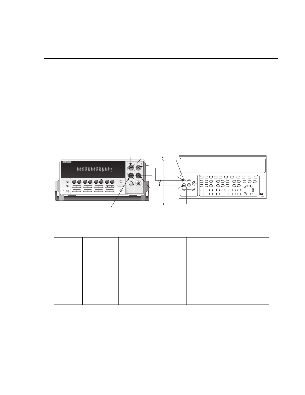
V erifying DC current
Check DC current accuracy by applying accurate DC currents from the DC current calibrator
to the AMPS input of the Model 2015 and v erifying that the displayed readings f all within specified limits.
Follow these steps to verify DC current accuracy:
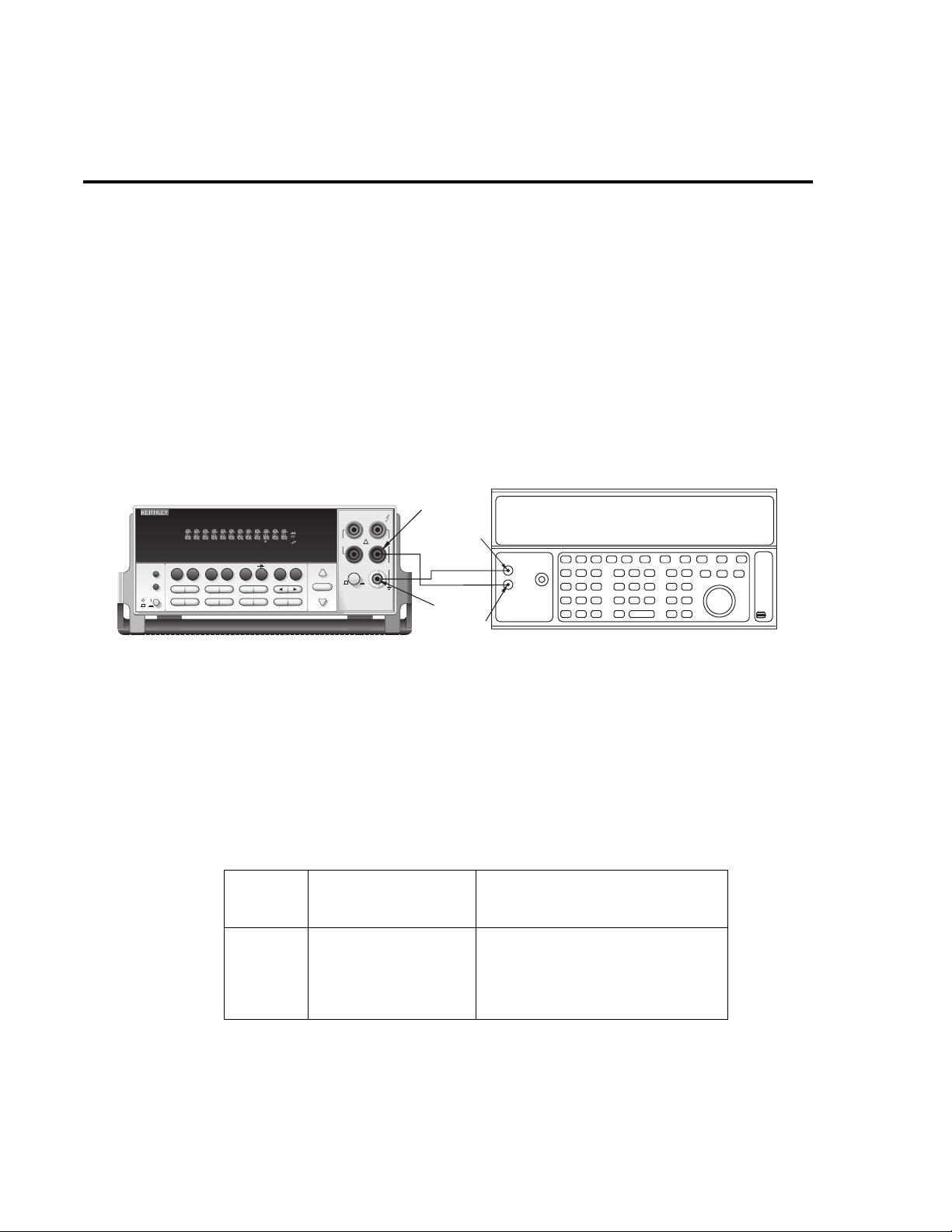
1. Connect the Model 2015 AMPS and INPUT LO jacks to the calibrator as shown in
Figure 1-3.
Figure 1-3
Connections for DC current verification
LOCAL
POWER
STEP CH2 CH3 CH4 CH5 CH6 CH7 CH8 CH9 CH10
TALK
LSTN
SRQ
SHIFT
TIMER
HOLD TRIG FAST MED SLOW AUTO ERR
MATH
DCV
EX TRIG
SAVE SETUP
SOURCE
THD
ACV
HOLD
TRIG
MEAS
THD
SHIFT
DC Current Calibrator
Model 2015
SCAN
CH1REM
REL FILT
dBm
dB
ACI
DCI
LIMITS ON/OFFDELAY
STORE
RECALL
CONFIG HALT
STEP SCAN
CONT
Ω2 Ω4
TEST
GPIB
DIGITS RATE
CAL
RELFILTER
RS232
MATH
REAR
4W
BUFFER
STAT
2015 THD MULTIMETER
PERIOD TCOUPL
FREQ
TEMP
EXIT ENTER
RANGE
RANGE
SENSE
INPUT
Ω 4 WIRE
HI
350V
!
PEAK
LO
INPUTS
F
R
AUTO
FRONT/REAR
3A 250V
AMPS
1000V
PEAK
500V
PEAK
Input
LO
Output HI
Amps
Output
LO
Note: Be sure calibrator is set for
normal current output.
2. Select the DC current measurement function by pressing the DCI key, then choose the
SLOW integration rate with the RATE key.
3. Set the Model 2015 for the 10mA range.
4. Source positive and negati ve full-scale currents for each of the ranges listed in Table
1-4, and verify that the readings for each range are within stated limits.
Table 1-4
DCI limits
DCI
range Applied DC current* Reading limits (1 year, 18°C-28°C)
10mA
100mA
1A
3A
10.0000mA
100.0000mA
1.000000A
2.20000A
9.99460 to 10.00540mA
99.9100 to 100.0900mA
0.999160 to 1.000840A
2.197315 to 2.202685A
*Source positive and negative currents with values shown.
Page 27
V erifying AC current
Check AC current accuracy by applying accurate AC voltage current at specific frequencies
from the A C current calibrator to the Model 2015 input and v erifying that the displayed readings
fall within specified limits. Follow these steps to verify AC current:
1. Connect the Model 2015 AMPS and INPUT LO jacks to the calibrator as shown in
Figure 1-4.
Figure 1-4
Connections for AC current verification
Model 2015
SENSE
SHIFT
LOCAL
POWER
MATH
DCV
EX TRIG
SOURCE
TALK
LSTN
SRQ
SHIFT
TIMER
SAVE SETUP
THD
SCAN
CH1REM
STEP CH2 CH3 CH4 CH5 CH6 CH7 CH8 CH9 CH10
HOLD TRIG FAST MED SLOW AUTO ERR
dBm
THD
ACV
DCI
HOLD
LIMITS ON/OFFDELAY
TRIG
STORE
RECALL
CONFIG HALT
MEAS
STEP SCAN
BUFFER
REL FILT
dB
CONT
ACI
Ω2 Ω4
TEST
CAL
RELFILTER
RS232
GPIB
DIGITS RATE
MATH
REAR
4W
STAT
2015 THD MULTIMETER
PERIOD TCOUPL
FREQ
TEMP
EXIT ENTER
RANGE
RANGE
Ω 4 WIRE
350V
PEAK
INPUTS
F
AUTO
FRONT/REAR
Amps
Performance Verification 1-13
INPUT
HI
!
LO
R
3A 250V
AMPS
1000V
PEAK
500V
PEAK
Output HI
Input
LO
Output
LO
AC Current Calibrator
2. Select the AC current function by pressing the ACI key , then choose the SLOW integration rate with the RATE key.
3. Set the Model 2015 for the 1A range.
4. Source 1A and 2.2A, 1kHz full-scale AC currents as summarized in Table 1-5, and
verify that the readings are within stated limits.
Table 1-5
ACI limits
ACV
range Applied AC voltage Reading limits @ 1kHz (1 year, 18°C-28°C)
1A
3A
1.000000A
2.20000A
0.99860 to 1.00140A
2.1949 to 2.2051A
Page 28
1-14 Performance Verification
V erifying resistance
Check resistance by connecting accurate resistance values to the Model 2015 and verifying
that its resistance readings are within the specified limits.
CAUTION Do not apply more than 1100V peak between INPUT HI and LO or more
than 350V peak between SENSE HI and LO, or instrument damage could
occur
Follow these steps to verify resistance accuracy:
1. Using shielded 4-wire connections, connect the Model 2015 INPUT and SENSE jacks
to the calibrator as shown in Figure 1-5.
.
Ω
Ω
Figure 1-5
Connections for resistance verification (100
Sense HI
Model 2015
SENSE
LOCAL
POWER
STEP CH2 CH3 CH4 CH5 CH6 CH7 CH8 CH9 CH10
TALK
LSTN
SRQ
SHIFT
TIMER
HOLD TRIG FAST MED SLOW AUTO ERR
MATH
DCV
EX TRIG
SAVE SETUP
SOURCE
THD
ACV
HOLD
TRIG
MEAS
THD
SHIFT
SCAN
CH1REM
REL FILT
dBm
dB
CONT
ACI
Ω2 Ω4
DCI
LIMITS ON/OFFDELAY
STORE
RECALL
CONFIG HALT
STEP SCAN
DIGITS RATE
MATH
REAR
4W
BUFFER
STAT
2015 THD MULTIMETER
PERIOD TCOUPL
FREQ
TEMP
TEST
CAL
RELFILTER
RS232
GPIB
EXIT ENTER
RANGE
RANGE
Ω 4 WIRE
350V
PEAK
INPUTS
F
AUTO
FRONT/REAR
Sense LO
2. Set the calibrator for 4-wire resistance with external sense on.
3. Select the Model 2015 4-wire resistance function by pressing the
the SLOW integration rate with the RATE key.
4. Set the Model 2015 for the 100
5. Recalculate reading limits based on actual calibrator resistance values.
Ω
-10M
Ω
ranges)
Sense HI
INPUT
HI
!
LO
R
3A 250V
AMPS
Input
HI
1000V
PEAK
500V
PEAK
Input
LO
Output
HI
Output
LO
Resistance Calibrator
Sense LO
Note: Use shielded low-thermal cables to
minimize noise. Enable or disable
calibrator external sense as indicated
in procedure.
4 key, then choose
range, and make sure the FILTER is on.
Page 29
6. Source the nominal full-scale resistance values for the 100 Ω -10M Ω ranges summarized
in Table 1-6, and verify that the readings are within calculated limits.
7. Connect the Model 2015 INPUT and SENSE jacks to the calibrator as shown in
Figure 1-6.
8. Disable external sense on the calibrator.
9. Set the Model 2015 for the 100M
10. Source a nominal 100M Ω resistance value, and verify that the reading is within calculated limits for the 100M Ω range.
Figure 1-6
Connections for resistance verification (100M
Ω
range)
range.
Performance Verification 1-15
Ω
Ω
1k Ω
Model 2015
Ω2 Ω4
TEST
GPIB
CAL
RELFILTER
RS232
MATH
REAR
BUFFER
STAT
2015 THD MULTIMETER
PERIOD TCOUPL
FREQ
EXIT ENTER
4W
TEMP
POWER
TALK
LSTN
SRQ
SHIFT
TIMER
MATH
SHIFT
DCV
LOCAL
EX TRIG
SAVE SETUP
SOURCE
THD
SCAN
CH1REM
STEP CH2 CH3 CH4 CH5 CH6 CH7 CH8 CH9 CH10
HOLD TRIG FAST MED SLOW AUTO ERR
REL FILT
dBm
dB
DCI
LIMITS ON/OFFDELAY
STORE
CONFIG HALT
STEP SCAN
RECALL
CONT
ACI
DIGITS RATE
THD
ACV
HOLD
TRIG
MEAS
Sense LO
Table 1-6
Limits for resistance verification
Nominal
Range
100 Ω
resistance
100Ω
1kΩ
10k Ω
100kΩ
1MΩ
10MΩ
100MΩ
10kΩ
100kΩ
1MΩ
10MΩ
100MΩ
Sense HI
RANGE
AUTO
RANGE
SENSE
INPUT
Ω 4 WIRE
HI
350V
!
PEAK
LO
INPUTS
F
R
FRONT/REAR
3A 250V
AMPS
Input
HI
1000V
PEAK
500V
PEAK
Input
LO
Output
HI
Output
LO
Resistance Calibrator
Note: Use shielded cables to minimize noise.
Disable calibrator external sense mode.
Nominal reading limits
(1 year, 18°C-28°C) Recalculated limits*
99.9860 to 100.0140Ω
0.999890 to 1.000110kΩ
9.99890 to 10.00110kΩ
99.9890 to 100.0110kΩ
0.999890 to 1.000110MΩ
9.99590 to 10.00410MΩ
99.8470 to 100.1530MΩ
__________ to __________ Ω
__________ to __________ kΩ
__________ to __________ kΩ
__________ to __________ kΩ
__________ to __________ MΩ
__________ to __________ MΩ
__________ to __________ MΩ
* Calculate limits based on actual calibration resistance values and Model 2015 one-year accuracy
specifications. See Verification limits.
Page 30

1-16 Performance Verification
V erifying temperature
Thermocouple temperature readings are derived from DC volts measurements. For that reason, it is not necessary to independently verify the accuracy of temperature measurements. As
long as the DC volts function meets or exceed its specifications, temperature function accuracy
is automatically verified. Howe ver, temperature verification procedures are provided below for
those who wish to separately verify temperature accuracy.
1. Connect the DC voltage calibrator output terminals to the Model 2015 INPUT jacks
using low-thermal shielded connections. (Use 2-wire connections similar to those sho wn
in Figure 1-1.)
2. Configure the Model 2015 for °C units, type J temperature sensor, and 0°C simulated reference junction as follows:
A. Press SHIFT then SENSOR, and note the unit displays the temperature units:
UNITS: C. (If necessary, use the cursor and range keys to select °C units.)
B. Press ENTER. The unit then displays the thermocouple type: TYPE: J.
C. Select a type J temperature sensor, then press ENTER. The unit then displays the
reference junction type: JUNC: SIM.
D. Make certain that the simulated reference junction type is selected, then press
ENTER. The unit then displays the current simulated reference junction tempera-
ture: SIM: 023.
E. Using the cursor and range keys, set the reference junction temperature to 0°C, then
press ENTER to complete the temperature configuration process.
3. Select the temperature function by pressing the TEMP key.
4. Source each of the voltages summarized in Table 1-7, and verify that the temperature readings are within limits. Be sure to select the appropriate thermocouple type
for each group of readings. (See step 2 above.)
Table 1-7
Thermocouple temperature verification reading limits
Thermocouple
type
J
K
* Voltages shown are based on ITS-90 standard using 0°C reference
junction temperature. See text for procedure to set reference junction
temperature.
Applied DC
voltage*
-7.659mV
0mV
42.280mV
-5.730mV
0mV
54.138mV
Reading limits
(1 year, 18°C-28°C)
-190.6 to -189.4°C
-0.5 to +0.5°C
749.5 to 750.5°C
-190.6 to -189.4°C
-0.5 to +0.5°C
1349.2 to 1350.8°C
Page 31

V erifying frequency
Follow the steps below to verify the Model 2015 frequency function:
1. Connect the frequency synthesizer to the Model 2015 INPUT jacks. (See Figure 1-7.)
2. Set the synthesizer to output a 1kHz, 1V RMS sine wave.
3. Select the Model 2015 frequency function by pressing the FREQ key.
4. Verify that the Model 2015 frequency reading is between 0.9999kHz and 1.0001kHz.
Figure 1-7
Connections for frequency verification
Performance Verification 1-17
SHIFT
LOCAL
POWER
TALK
LSTN
SRQ
SHIFT
TIMER
MATH
DCV
EX TRIG
SAVE SETUP
SOURCE
THD
Model 2015
SCAN
CH1REM
STEP CH2 CH3 CH4 CH5 CH6 CH7 CH8 CH9 CH10
REL FILT
CONT
Ω2 Ω4
TEST
GPIB
DIGITS RATE
BUFFER
PERIOD TCOUPL
FREQ
CAL
RELFILTER
RS232
HOLD TRIG FAST MED SLOW AUTO ERR
dBm
dB
THD
ACI
ACV
DCI
HOLD
LIMITS ON/OFFDELAY
TRIG
STORE
RECALL
CONFIG HALT
MEAS
STEP SCAN
MATH
REAR
4W
STAT
2015 THD MULTIMETER
TEMP
EXIT ENTER
RANGE
RANGE
BNC-to-Dual
Banana Plug
Frequency Synthesizer
Adapter
SENSE
INPUT
Ω 4 WIRE
HI
350V
1000V
!
PEAK
PEAK
LO
500V
PEAK
INPUTS
F
R
AUTO
FRONT/REAR
3A 250V
AMPS
Main
Function
Output
50Ω BNC Coaxial Cable
Page 32

1-18 Performance Verification
V erifying total harmonic distortion
Follow the steps below to verify the Model 2015 total harmonic distortion function.
1. Connect the low-distortion function generator to the Model 2015 INPUT jacks. (See
Figure 1-8.)
Figure 1-8
Connections for total harmonic distortion verification
BNC-to-Dual
Banana Plug
Adapter
INPUT
HI
1000V
!
PEAK
LO
500V
PEAK
R
3A 250V
AMPS
SHIFT
LOCAL
POWER
TALK
LSTN
SRQ
SHIFT
TIMER
MATH
DCV
EX TRIG
SAVE SETUP
SOURCE
THD
Model 2015
SCAN
CH1REM
STEP CH2 CH3 CH4 CH5 CH6 CH7 CH8 CH9 CH10
REL FILT
HOLD TRIG FAST MED SLOW AUTO ERR
dBm
THD
ACV
DCI
HOLD
LIMITS ON/OFFDELAY
TRIG
STORE
RECALL
CONFIG HALT
MEAS
STEP SCAN
BUFFER
dB
CONT
PERIOD TCOUPL
Ω2 Ω4
TEST
GPIB
DIGITS RATE
FREQ
CAL
RELFILTER
RS232
ACI
MATH
REAR
4W
STAT
2015THD MULTIMETER
TEMP
EXIT ENTER
RANGE
RANGE
SENSE
Ω 4 WIRE
350V
PEAK
INPUTS
F
AUTO
FRONT/REAR
Low Distortion Function Generator
Output
Coaxial Cable
2. Set the function generator to output a 1kHz, 0.95V RMS sine wave with an unbalanced,
high-impedance output.
3. Using the MEAS key, set the following operating modes:
TYPE: THD
FREQ: AUT O
UPR HARM: 10
UNITS: PERC
SFIL: NONE
4. Select the Model 2015 THD function by pressing SHIFT then THD.
5. Use the down RANGE key to select the 1V range.
6. Verify that the Model 2015 THD reading is <0.004%.
Page 33

V erifying function generator amplitude
Follow the steps below to verify Model 2015 function generator amplitude:
1. Connect the rear panel SOURCE OUTPUT jack to the front panel INPUT jacks. (See
Figure 1-9.)
Figure 1-9
Connections for function generator amplitude verification
Performance Verification 1-19
POWER
TALK
LSTN
SRQ
SHIFT
TIMER
MATH
SHIFT
DCV
LOCAL
EX TRIG
SAVE SETUP
SOURCE
THD
Model 2015
SCAN
CH1REM
STEP CH2 CH3 CH4 CH5 CH6 CH7 CH8 CH9 CH10
REL FILT
HOLD TRIG FAST MED SLOW AUTO ERR
dBm
THD
ACV
DCI
HOLD
LIMITS ON/OFFDELAY
TRIG
STORE
RECALL
CONFIG HALT
MEAS
STEP SCAN
BUFFER
dB
CONT
Ω2 Ω4
TEST
GPIB
DIGITS RATE
RS232
RELFILTER
PERIOD TCOUPL
CAL
ACI
MATH
REAR
4W
STAT
2015 THD MULTIMETER
FREQ
TEMP
EXIT ENTER
RANGE
RANGE
SENSE
INPUT
Ω 4 WIRE
HI
350V
1000V
!
PEAK
PEAK
LO
500V
PEAK
INPUTS
F
R
AUTO
FRONT/REAR
3A 250V
AMPS
Connect INPUT jacks to
rear panel SOURCE OUTPUT
2. Use the SOURCE key to set the function generator operating modes as follows:
SINE OUT: ON
FREQ: 1kHz
IMPEDANCE: HIZ
AMPL: 4.0000V
3. Press the ACV key to select the AC voltage function, and choose the 10V range.
4. Verify that the AC voltage reading is between 3.986V and 4.014V.
Page 34

2
Calibration
Page 35

2-2 Calibration
Introduction
Use the procedures in this section to calibrate the Model 2015. Calibration procedures
include:
• Comprehensive calibration: Usually the only calibration required in the field.
• Manufacturing calibration: Usually only performed at the factory (unless the unit has
been repaired).
WARNING This information in this section is intended only for qualified service per-
sonnel. Do not attempt these procedures unless you are qualified to do so.
All the procedures require accurate calibration equipment to supply precise DC and AC voltages, DC and A C currents, and resistance values. Comprehensi ve AC, DC, distortion, or function
generator calibration can be performed any time by an operator either from the front panel, or
by using the SCPI commands sent either over the IEEE-488 bus or the RS-232 port. DC-only,
distortion, and function generator calibration may be performed individually, if desired.
Page 36

Calibration 2-3
Environmental conditions
Conduct the calibration procedures in a location that has:
• An ambient temperature of 18° to 28°C (65° to 82°F)
• A relative humidity of less than 80% unless otherwise noted
W arm-up period
Allow the Model 2015 Multimeter to warm up for at least one hour before performing
calibration.
If the instrument has been subjected to temperature extremes (those outside the ranges stated
in the above section) allow e xtra time for the instrument’s internal temperature to stabilize. Typically, allow one extra hour to stabilize a unit that is 10°C (18°F) outside the specified temperature range.
Also, allow the test equipment to warm up for the minimum time specified by the
manufacturer.
Line power
The Model 2015 Multimeter requires a line voltage of 100V/120V/220V/240V, ±10% and a
line frequency of 45Hz to 66Hz, or 360Hz to 440Hz.
Page 37

2-4 Calibration
Calibration considerations
When performing the calibration procedures:
• Make sure that the equipment is properly warmed up and connected to the appropriate
input jacks. Also make sure that the correct input jacks are selected with the INPUTS
switch.
• Make sure the calibrator is in operate before you complete each calibration step.
• Always let the source signal settle before calibrating each point.
• Do not connect test equipment to the Model 2015 through a scanner or other switching
equipment.
• If an error occurs during calibration, the Model 2015 will generate an appropriate error
message. See
Appendix B for more information.
WARNING The maximum common-mode voltage (voltage between INPUT LO and
chassis ground) is 500 V peak. Exceeding this value may cause a breakdown in insulation, creating a shock hazard. Some of the procedures in this
section may expose you to dangerous voltages. Use standard safety precautions when such dangerous voltages are encountered to avoid personal
injury caused by electric shock.
CAUTION Do not exceed 1100V peak between INPUT HI and INPUT LO or 350V
peak between SENSE HI and SENSE LO. Exceeding these values may
result in instrument damage.
Page 38

Calibration code
Before performing comprehensive calibration, you must first unlock calibration by entering
the appropriate calibration code.
Front panel calibration code
For front panel calibration, follow these steps:
1. Access the calibration menu by pressing SHIFT CAL, and note that the instrument displays the following:
CAL: DATES
2. Use the up or down range key to scroll through the a v ailable calibration parameters until
the unit displays RUN, then press ENTER.
3. The Model 2015 then prompts you to enter a code:
CODE? 000000
(The factory default code is 002015.) Use the left and right arrow keys to move among
the digits; use the up range key to increment numbers, and press the down range key to
specify alphabetic letters. Confirm the code by pressing ENTER.
4. The Model 2015 allows you to define a new calibration code. Use the up and do wn range
keys to toggle between yes and no. Choose N if you do not want to change the code.
Choose Y if you want to change the code. The unit then prompts you to enter a new code.
Enter the code, and press ENTER.
Calibration 2-5
Remote calibration code
If you are performing calibration over the IEEE-488 bus or the RS-232 port, send this com-
mand to unlock calibration:
:CAL:PROT:CODE '<8-character string>'.
The default code command is:
:CAL:PROT:CODE 'KI002015'.
Page 39

Ω
Ω
Ω
Ω
2-6 Calibration
Comprehensive calibration
The comprehensive calibration procedure calibrates the DCV, DCI, ACV, ACI, ohms, and
generator functions You can also choose to calibrate only the DCV/DCI and resistance, ACV/
ACI, distortion, or generator functions.
These procedures are usually the only ones required in the field. Manufacturing calibration is
normally done only at the factory, but it should also be done in the field if the unit has been
repaired. See
Calibration cycle
Perform comprehensive calibration at least once a year, or every 90 days to ensure the unit
meets the corresponding specifications.
Manufacturing calibration at the end of this section for more information.
Recommended equipment
T able 2-1 lists the recommended equipment you need for comprehensive, DC only, A C only,
distortion, and generator calibration procedures. You can use alternate equipment, such as a DC
transfer standard and characterized resistors, as long that equipment has specifications at least
as good as those listed in the table.
Table 2-1
Recommended equipment for comprehensive calibration
Fluke 5700A Calibrator:
AC voltage
DC voltage
10V:±5ppm
100V: ±ppm
Stanford Research Systems DS-360 Ultra Low Distortion Function Generator:
1V RMS sine wave @ 137Hz, -100dB THD
1V RMS sine wave @ 844Hz, -100dB THD
Miscellaneous equipment:
Keithley 8610 low-thermal shorting plug
Double banana plug to double banana plug shielded cable
BNC to double banana plug shielded cable
(1kHz, 50kHz)* DC current
10mV:±710ppm
100mV:±200ppm
1V:±82ppm
10V:±82ppm
100V:±90ppm
700V:±85ppm
10mA:±60ppm
100mA:±70ppm
1A:±110ppm
AC current
(1kHz) Resistance
100mA:±190ppm
1A:±690ppm
2A:±670ppm
1k
10k
100k
1M
:±12ppm
:±11ppm
:±13ppm
:±18ppm
* 1kHz specifications. 10mV and 700V points require 1kHz only.
All calibrator specifications are 90-day, 23°C ±5°C specifications and indicate total absolute uncertainty at
specified output.
Page 40

Aborting calibration
You can abort the front panel calibration process at any time by pressing EXIT. The instru-
ment will then ask you to confirm your decision to abort with the following message:
ABORT CAL?
Press EXIT to abort calibration at this point, or press any other key to return to the calibration
process.
NOTE The Model 2015 will not respond to any remote programming commands while the
ABORT CAL? message is displayed.
Calibration 2-7
Front panel calibration
Follow the steps in the following paragraphs for comprehensive, DC only, AC only, distor-
tion, and function generator calibration procedures.
The procedures for front panel calibration include:
• Preparing the Model 2015 for calibration
• Front panel short and open calibration
• DC voltage calibration
• Resistance calibration
• DC current calibration
• AC voltage calibration
• AC current calibration
• Distortion calibration
• Function generator calibration
• Setting calibration dates
Preparing the Model 2015 for calibration
1. Turn on the Model 2015, and allo w it to warm up for at least one hour before performing
calibration procedure.
2. Select the DCV function, and choose SLOW as the RATE (integration time = 10 PLC).
3. Start the calibration process as follows:
A. Access the calibration menu by pressing SHIFT then CAL.
B. Use the up and down range keys to scroll through the available calibration menu
items until the unit displays RUN, then press ENTER.
C. At the prompt, enter the calibration code. (The default code is 002015.) Use the left
and right arrow keys to move among the digits; use the up range key to increment
numbers, and press the down range key to specify alphabetic letters. Confirm the
code by pressing ENTER.
D. Choose N at the prompt to proceed without changing the code, then press ENTER.
Page 41

2-8 Calibration
4. Choose which of the calibration tests summarized in Table 2-2 you want to run at the
CAL: RUN prompt. Use the up and do wn range keys to scroll through the options; select
your choice by pressing ENTER.
Table 2-2
Comprehensive calibration procedures
Procedure Menu choice Procedures
Full calibration
DCV, DCI, and ohms
ACV and ACI
Distortion
Function generator*
ALL
DC
AC
DIST
FGEN
All comprehensive calibration steps. (DC, AC, DIST, FGEN)
DC voltage, DC current, and resistance calibration.
AC voltage and AC current.
Calibrate distortion.
Calibrate function generator.
*Perform AC calibration first if distortion or function generator calibration is done separately.
Front panel short and open calibration
At the Model 2015 prompt for a front panel short, do the following:
1. Connect the Model 8610 low-thermal short to the instrument front panel INPUT and
SENSE terminals as shown in Figure 2-1. Make sure the INPUTS b utton is not pressed
in so that the front inputs are selected. Wait at least three minutes before proceeding to
allow for thermal equilibrium.
Figure 2-1
Low-thermal short connections
HI
INPUT
HI
1000V
!
PEAK
LO
500V
PEAK
R
3A 250V
AMPS
Model 8610
Low-thermal
short
LOCAL
POWER
TALK
LSTN
SRQ
SHIFT
TIMER
MATH
SHIFT
DCV
EX TRIG
SAVE SETUP
SOURCE
THD
Model 2015
SCAN
CH1REM
STEP CH2 CH3 CH4 CH5 CH6 CH7 CH8 CH9 CH10
HOLD TRIG FAST MED SLOW AUTO ERR
dBm
THD
ACI
ACV
DCI
HOLD
LIMITS ON/OFFDELAY
TRIG
STORE
RECALL
CONFIG HALT
MEAS
STEP SCAN
BUFFER
REL FILT
dB
CONT
PERIOD TCOUPL
FREQ
Ω2 Ω4
TEST
CAL
RELFILTER
RS232
GPIB
DIGITS RATE
MATH
REAR
4W
STAT
2015 THD MULTIMETER
TEMP
EXIT ENTER
RANGE
RANGE
S+
SENSE
Ω 4 WIRE
350V
PEAK
INPUTS
F
AUTO
FRONT/REAR
S-
LO
NOTE Be sure to connect the low-thermal short properly to the HI, LO, and SENSE termi-
nals. Keep drafts away from low-thermal connections to avoid thermal drift, which
could affect calibration accuracy.
Page 42

2. Press ENTER to start short-circuit calibration. While the unit is calibrating, it will
display:
CALIBRATING
3. When the unit is done calibrating, it will display the following prompt:
OPEN CIRCUIT
4. Remove the calibration short, and press ENTER. During this phase, the CALIBRATING message will be displayed.
DC volts calibration
After the front panel short and open procedure, the unit will prompt you for the first DC volt-
age: +10V. Do the following:
Calibration 2-9
1. Connect the calibrator to the Model 2015 as shown in Figure 2-2. Wait three minutes to
allow for thermal equilibrium before proceeding.
Figure 2-2
Connections for DC volts and ohms calibration
Sense HI
Model 2015
SENSE
INPUT
Ω 4 WIRE
HI
350V
!
PEAK
LO
INPUTS
F
R
FRONT/REAR
3A 250V
AMPS
LOCAL
POWER
TALK
LSTN
SRQ
SHIFT
TIMER
MATH
SHIFT
DCV
EX TRIG
SAVE SETUP
SOURCE
THD
SCAN
CH1REM
STEP CH2 CH3 CH4 CH5 CH6 CH7 CH8 CH9 CH10
HOLD TRIG FAST MED SLOW AUTO ERR
dBm
THD
ACI
ACV
DCI
HOLD
LIMITS ON/OFFDELAY
TRIG
STORE
RECALL
CONFIG HALT
MEAS
STEP SCAN
BUFFER
REL FILT
dB
CONT
PERIOD TCOUPL
Ω2 Ω4
TEST
CAL
RELFILTER
RS232
GPIB
DIGITS RATE
MATH
REAR
4W
STAT
2015 THD MULTIMETER
FREQ
TEMP
EXIT ENTER
RANGE
RANGE
AUTO
Sense LO
NOTE Although 4-wire connections are shown, the sense leads are connected and discon-
nected at various points in this procedure by turning calibrator external sense on or
off as appropriate. If your calibrator does not have provisions for turning external
sense on and off, disconnect the sense leads when external sensing is to be turned of f,
and connect the sense leads when external sensing is to be turned on.
Sense HI
DC Voltage Calibrator
Input
HI
1000V
PEAK
500V
PEAK
Input
LO
Output
HI
Output
LO
Sense LO
Note: Use shielded low-thermal cables to
minimize noise. Enable or disable
calibrator external sense as indicated
in procedure.
2. Set the calibrator to output DC volts, and turn external sense off.
Page 43

2-10 Calibration
3. Perform the steps listed in Table 2-3 to complete DC volts calibration. For each calibration step:
• Set the calibrator to the indicated value, and make sure it is in operate.
• Press the ENTER key to calibrate that step.
• Wait until the Model 2015 finishes each step. (The unit will display the CALI-
BRATING message while calibrating.)
NOTE If your calibrator cannot output the values recommended in T able 2-3, use the left and
right arrow ke ys, and the up and down rang e keys to set the Model 2015 display value
to match the calibrator output voltage.
Table 2-3
DC volts calibration summary
Calibration
step
+10V
-10V
100V
Calibrator
voltage Allowable range
+10.00000V
-10.00000V
+100.0000V
+9V to +11V
-9V to -11V
+90V to +110V
Page 44

Resistance calibration
Completing the 100V DC calibration step ends the DC voltage calibration procedure. The
Model 2015 will then prompt you to connect 1k
1. Set the calibrator output for resistance, and turn on external sense.
Ω
1k Ω
1M Ω 1k Ω
1M Ω
9k Ω
Calibration 2-11
. Follow these steps for resistance calibration:
NOTE Use external sense (4-wire
calibrator external sense mode is turned on.
2. Perform the calibration steps summarized in Table 2-4. For each step:
• Set the calibrator to the indicated value, and place the unit in operate. (If the calibrator cannot output the exact resistance value, use the Model 2015 left and right
arrow keys and the range keys to adjust the Model 2015 display to agree with the
calibrator resistance.)
• Press the ENTER key to calibrate each point.
• Wait for the Model 2015 to complete each step before continuing.
Table 2-4
Ohms calibration summary
Calibration
step
Calibrator
resistance* Allowable range
Ω
) when calibrating all resistance r anges. Be sur e that the
0.9k Ω to 1.1k Ω
10k Ω
100k Ω
10k Ω
100k Ω
to 11k Ω
90k Ω to 110k Ω
0.9M Ω to 1.1M Ω
* Nominal resistance. Adjust Model 2015 calibration
parameter to agree with actual value.
Page 45

2-12 Calibration
DC current calibration
After the 1M Ω resistance point has been calibrated, the unit will prompt you for 10mA. Fol-
low these steps for DC current calibration:
1. Connect the calibrator to the AMPS and INPUT LO terminals of the Model 2015 as
shown in Figure 2-3.
Figure 2-3
Connections for DC and AC amps calibration
Model 2015
SENSE
Ω 4 WIRE
HI
350V
!
PEAK
LO
INPUTS
F
R
AUTO
FRONT/REAR
LOCAL
POWER
STEP CH2 CH3 CH4 CH5 CH6 CH7 CH8 CH9 CH10
TALK
LSTN
SRQ
SHIFT
TIMER
HOLD TRIG FAST MED SLOW AUTO ERR
MATH
THD
SHIFT
DCV
ACV
HOLD
TRIG
EX TRIG
SAVE SETUP
SOURCE
MEAS
THD
SCAN
CH1REM
REL FILT
dBm
dB
CONT
ACI
Ω2 Ω4
DCI
LIMITS ON/OFFDELAY
STORE
RECALL
CONFIG HALT
STEP SCAN
DIGITS RATE
MATH
REAR
4W
BUFFER
STAT
2015 THD MULTIMETER
PERIOD TCOUPL
FREQ
TEMP
EXIT ENTER
RANGE
RANGE
TEST
CAL
RELFILTER
RS232
GPIB
Current Calibrator
Input
1000V
PEAK
500V
PEAK
LO
Output HI
INPUT
3A 250V
AMPS
Amps
Output
LO
Note: Be sure calibrator is set for
normal current output.
2. Calibrate each current step summarized in Table 2-5. For each step:
• Set the calibrator to the indicated DC current, and make sure the unit is in operate.
• Make sure the Model 2015 display indicates the correct calibration current.
• Press ENTER to complete each step.
• Allow the Model 2015 to finish each step.
NOTE If you are performing DC-only calibration, proceed to Setting calibration dates.
Table 2-5
DC current calibration summary
Calibrator
Calibration step
10mA
100mA
1A
current Allowable range
10.00000mA
100.0000mA
1.000000A
9mA to 11mA
90mA to 110mA
0.9A to 1.1A
Page 46

AC voltage calibration
Follow these steps for AC voltage calibration:
1. Connect the calibrator to the Model 2015 INPUT HI and LO terminals as shown in
Figure 2-4.
Figure 2-4
Connections for AC volts calibration
Model 2015
LOCAL
POWER
TALK
LSTN
SRQ
SHIFT
TIMER
MATH
SHIFT
DCV
EX TRIG
SAVE SETUP
SOURCE
THD
SCAN
CH1REM
STEP CH2 CH3 CH4 CH5 CH6 CH7 CH8 CH9 CH10
HOLD TRIG FAST MED SLOW AUTO ERR
REL FILT
dBm
dB
DCI
LIMITS ON/OFFDELAY
STORE
CONFIG HALT
STEP SCAN
RECALL
CONT
ACI
DIGITS RATE
THD
ACV
HOLD
TRIG
MEAS
Ω2 Ω4
TEST
GPIB
CAL
RELFILTER
RS232
MATH
REAR
BUFFER
STAT
2015 THD MULTIMETER
PERIOD TCOUPL
FREQ
TEMP
EXIT ENTER
4W
RANGE
AUTO
RANGE
Calibration 2-13
Input HI
SENSE
INPUT
Ω 4 WIRE
HI
350V
!
PEAK
LO
INPUTS
F
R
FRONT/REAR
3A 250V
AMPS
1000V
PEAK
500V
PEAK
Output HI
Input
AC Voltage Calibrator
LO
Output
LO
2. Perform the calibration steps summarized in Table 2-6. For each step:
• Set the calibrator to the indicated value, and make sure the calibrator is in operate.
• Press ENTER to complete each step.
• Wait until the Model 2015 completes each step.
Table 2-6
AC voltage calibration summary
Calibration step Calibrator voltage, frequency
10mV AC at 1kHz
100mV AC at 1kHz
100mV AC at 50kHz
1V AC at 1kHz
1V AC at 50kHz
10V AC at 1kHz
10V AC at 50kHz
100V AC at 1kHz
100V AC at 50kHz
700V AC at 1kHz
10.00000mV, 1kHz
100.0000mV, 1kHz
100.0000mV, 50kHz
1.000000V, 1kHz
1.000000V, 50kHz
10.00000V, 1kHz
10.00000V, 50kHz
100.0000V, 1kHz
100.0000V, 50kHz
700.000V, 1kHz
Page 47

2-14 Calibration
AC current calibration
After the 700VAC at 1kHz point has been calibrated, the unit will prompt you for 100mA at
1kHz. Follow these steps for AC current calibration:
1. Connect the calibrator to the AMPS and INPUT LO terminals of the Model 2015 as
shown in Figure 2-3.
2. Perform the calibration steps summarized in Table 2-7. For each step:
• Set the calibrator to the indicated current and frequency, and make sure the unit is
in operate.
• Press ENTER to complete each calibration step.
• Allow the unit to complete each step before continuing.
Table 2-7
AC current calibration summary
Calibration step Calibrator current, frequency
100mA at 1kHz
1A at 1kHz
2A at 1kHz
Distortion calibration
1. Following A C current calibration, the Model 2015 will prompt you for the first distortion
calibration point (see Table 2-8):
1V AT 137 HZ
2. Connect the low-distortion function generator to the front panel INPUT jacks (see Figure
2-5).
3. Set the function generator to output a 1V RMS sine wave at a frequency of 137Hz.
4. Press the Model 2015 ENTER key to complete the 137Hz calibration step. The unit will
prompt you for the second distortion calibration point:
1V AT 844 HZ
5. Set the function generator to output a 1V RMS sine wave at a frequency of 844Hz.
6. Press ENTER to complete the 844Hz calibration step.
100.0000mA, 1kHz
1.000000A, 1kHz
2.000000A, 1kHz
Page 48

Figure 2-5
Connections for distortion calibration
Calibration 2-15
Model 2015
SENSE
LOCAL
POWER
STEP CH2 CH3 CH4 CH5 CH6 CH7 CH8 CH9 CH10
TALK
LSTN
SRQ
SHIFT
TIMER
HOLD TRIG FAST MED SLOW AUTO ERR
MATH
THD
SHIFT
DCV
ACV
HOLD
EX TRIG
TRIG
SAVE SETUP
SOURCE
MEAS
THD
Ω2 Ω4
TEST
GPIB
CAL
RELFILTER
RS232
MATH
REAR
BUFFER
STAT
2015 THD MULTIMETER
PERIOD TCOUPL
FREQ
EXIT ENTER
4W
TEMP
SCAN
CH1REM
REL FILT
dBm
dB
CONT
ACI
DCI
LIMITS ON/OFFDELAY
STORE
RECALL
CONFIG HALT
STEP SCAN
DIGITS RATE
RANGE
RANGE
Ω 4 WIRE
350V
PEAK
INPUTS
F
AUTO
FRONT/REAR
Table 2-8
Distortion and function generator calibration summary
Calibration step Calibration signal or connections
Distortion, 1V at 137Hz
Distortion, 1V at 844Hz
Function generator
Function generator calibration
1. Following distortion calibration, the Model 2015 will prompt you to connect the
SOURCE OUTPUT jack to the INPUT jacks:
INPUT FGEN
2. Connect the rear panel SOURCE OUTPUT jack to the front panel INPUT jacks (See
Figure 2-6.)
3. Press the ENTER key to complete function generator calibration.
INPUT
HI
!
LO
R
3A 250V
AMPS
BNC-to-Dual
Banana Plug
Adapter
1000V
PEAK
500V
PEAK
Low Distortion Function Generator
Output
Coaxial Cable
1V RMS, 137Hz sine wave
1V RMS, 844Hz sine wave
SOURCE OUTPUT to INPUT
Figure 2-6
Connections for function generator calibration
Model 2015
Ω2 Ω4
TEST
GPIB
CAL
RELFILTER
RS232
MATH
REAR
4W
BUFFER
STAT
2015 THD MULTIMETER
PERIOD TCOUPL
FREQ
TEMP
EXIT ENTER
POWER
TALK
LSTN
SRQ
SHIFT
TIMER
MATH
SHIFT
DCV
LOCAL
EX TRIG
SAVE SETUP
SOURCE
THD
SCAN
CH1REM
STEP CH2 CH3 CH4 CH5 CH6 CH7 CH8 CH9 CH10
HOLD TRIG FAST MED SLOW AUTO ERR
REL FILT
dBm
dB
DCI
LIMITS ON/OFFDELAY
STORE
CONFIG HALT
STEP SCAN
RECALL
CONT
ACI
DIGITS RATE
THD
ACV
HOLD
TRIG
MEAS
RANGE
RANGE
Connect INPUT jacks to
SENSE
INPUT
Ω 4 WIRE
HI
350V
1000V
!
PEAK
PEAK
LO
500V
PEAK
INPUTS
F
R
AUTO
FRONT/REAR
3A 250V
AMPS
rear panel SOURCE OUTPUT
Page 49

2-16 Calibration
Setting calibration dates and saving calibration
Remote calibration
At the end of the calibration procedure, the instrument will display the CALIBRATION
COMPLETE message. Press ENTER to continue, and the Model 2015 will prompt you to enter
the calibration date and the calibration due date. Set these dates as follows:
1. At the CAL DATE: mm/dd/yy prompt, use the left and right arrow keys, and the range
keys to set the calibration date, then press ENTER.
2. The unit will then prompt you to enter the next calibration due date with this prompt:
CAL NDUE: mm/dd/yy . Use the left and right arrow keys, and the range keys to set the
calibration due date, then press ENTER.
3. The unit will prompt you to save new calibration constants with this message: SAVE
CAL? YES. To save the new constants, press ENTER. If you do not want to save the
new constants, press the down range key to toggle to NO, then press ENTER.
NOTE Calibration constants calculated during the curr ent calibr ation procedur e will not be
saved unless you choose the YES option. Previous calibration constants will be
retained if you select NO.
Follow the steps in this section to perform comprehensi ve procedures via remote. See Appen-
dix B for a detailed list and description of remote calibration commands.
When sending calibration commands, be sure that the Model 2015 completes each step before
sending the next command. You can do so either by observing the front panel CALIBRATING
message, or by detecting the completion of each step over the bus. (See Detecting calibration
step completion in Appendix B.)
The procedures for calibrating the Model 2015 via remote include:
• Preparing the Model 2015 for calibration
• Front panel short and open calibration
• DC volts calibration
• Resistance calibration
• DC current calibration
• AC volts calibration
• AC current calibration
• Distortion calibration
• Function generator calibration
• Programming calibration dates
• Saving calibration constants
• Locking out calibration
NOTE As with fr ont panel calibr ation, you can c hoose to perform comprehensive, DC-only,
AC-only, distortion, or function generator calibration. Be sure to include a space
character between each command and parameter.
Page 50

Preparing the Model 2015 for calibration
1. Connect the Model 2015 to the IEEE-488 bus of the computer using a shielded
IEEE-488 cable, such as the Keithley Model 7007, or connect the unit to a computer
through the RS-232 port using a straight-through 9-pin to 9-pin cable (use a 9-25-pin
adapter if necessary).
2. Turn on the Model 2015, and allow it to warm up for an hour before performing
calibration.
3. Select the DCV function, and choose SLOW as the rate (integration time = 10PLC).
4. Make sure the primary address of the Model 2015 is the same as the address specified in
the program that you will be using to send commands. (Use the GPIB key.)
5. Unlock the calibration function by sending this command:
:CAL:PROT:CODE 'KI002015'
(The above command shows the default code, KI002015. Substitute the correct code if
changed.)
6. Send the following command to initiate calibration:
:CAL:PROT:INIT
Short and open calibration
Calibration 2-17
1. Connect the Model 8610 low-thermal short to the instrument INPUT and SENSE terminals as shown in Figure 2-1. Make sure the INPUTS b utton is not pressed in so that the
front inputs are active. W ait at least three minutes before proceeding to allo w for thermal
equilibrium.
NOTE Be sure to connect the low-thermal short properly to the HI, LO, and SENSE termi-
nals. Keep drafts away from low-thermal connections to avoid thermal drift, which
could affect calibration accuracy.
2. Send the following command:
:CAL:PROT:DC:STEP1
3. After the Model 2015 completes this step, remove the low-thermal short, and send this
command:
:CAL:PROT:DC:STEP2
Page 51

2-18 Calibration
DC volts calibration
After front panel short and open steps, do the following:
1. Connect the calibrator to the Model 2015 as shown in Figure 2-2. Allow three minutes
for thermal equilibrium.
NOTE Although 4-wire connections are shown, the sense leads are connected and discon-
nected at various points in this procedure by turning calibrator external sense on or
off as appropriate. If your calibrator does not have provisions for turning external
sense on and off, disconnect the sense leads when external sensing is to be turned of f,
and connect the sense leads when external sensing is to be turned on.
2. Perform the calibration steps summarized in Table 2-9. For each step:
• Set the calibrator to the indicated voltage, and make sure the unit is in operate. (Use
the recommended voltage if possible.)
• Send the indicated programming command. (Change the voltage parameter if you
are using a different calibration voltage.)
• Wait until the Model 2015 completes each step before continuing.
Table 2-9
DC voltage calibration programming steps
Calibration
step
+10V
-10V
100V
* Use recommended value where possible. Change parameter accordingly if using a
different calibrator voltage.
Calibrator
voltage Calibration command* Parameter range
+10.00000V
-10.00000V
100.0000V
:CAL:PROT:DC:STEP3 10
:CAL:PROT:DC:STEP4 10
:CAL:PROT:DC:STEP5 100
9 to 11
-9 to -11
90 to 110
Page 52

Resistance calibration
Follow these steps for resistance calibration:
1. Set the calibrator to the resistance mode, and turn on external sensing.
Calibration 2-19
NOTE Use external sense (4-wir e
calibrator external sense mode is turned on.
2. Perform the calibration steps summarized in Table 2-10. For each step:
• Set the calibrator to the indicated resistance, and make sure the unit is in operate.
(Use the recommended resistance or the closest available value.)
• Send the indicated programming command. (Change the command parameter if
you are using a different calibration resistance than that shown.)
• Wait until the Model 2015 completes each step before continuing.
Table 2-10
Resistance calibration programming steps
Calibration
step
1kΩ
10kΩ
100kΩ
1MΩ
* Use exact calibrator resistance value for parameter.
Calibrator
resistance Calibration command* Parameter range
1kΩ
10kΩ
100kΩ
1MΩ
Ω
) when calibrating all resistance r anges. Be sur e that the
:CAL:PROT:DC:STEP6 1E3
:CAL:PROT:DC:STEP7 10E3
:CAL:PROT:DC:STEP8 100E3
:CAL:PROT:DC:STEP9 1E6
900 to 1.1E3
9E3 to 11E3
90E3 to 110E3
900E3 to 1.1E6
Page 53

2-20 Calibration
DC current calibration
After the 1MΩ resistance point has been calibrated, follow these steps for DC current
calibration:
1. Connect the calibrator to the AMPS and INPUT LO terminals of the Model 2015 as
shown in Figure 2-3.
2. Perform the calibration steps listed in Table 2-11. For each step:
• Set the calibrator to the indicated current, and make sure the unit is in operate. (Use
the recommended current if possible.)
• Send the indicated programming command. (Change the current parameter if you
are using a different calibration current.)
• Wait until the Model 2015 completes each step before continuing.
NOTE If you are performing DC-only calibration, proceed to Programming calibration
dates.
Table 2-11
DC current calibration programming steps
Calibration
step
10mA
100mA
1A
* Change parameter if using different current.
Calibrator
current Calibration command* Parameter range
10.00000mA
100.00000mA
1.000000A
:CAL:PROT:DC:STEP10 10E-3
:CAL:PROT:DC:STEP11 100E-3
:CAL:PROT:DC:STEP12 1
9E-3 to 11E-3
90E-3 to 110E-3
0.9 to 1.1
Page 54

AC voltage calibration
Follow these steps for AC voltage calibration:
1. Connect the calibrator to the Model 2015 INPUT HI and LO terminals as shown in
Figure 2-4.
2. Perform the calibration steps summarized in Table 2-12. For each step:
• Set the calibrator to the indicated voltage and frequency, and make sure the unit is
in operate. (You must use the stated voltage and frequency.)
• Send the indicated programming command.
• Wait until the Model 2015 completes each step before continuing.
Table 2-12
AC voltage calibration programming steps
Calibration step
Calibration 2-21
Calibrator voltage,
frequency Calibration command
10mV AC at 1kHz
100mV AC at 1kHz
100mV AC at 50kHz
1VAC at 1kHz
1VAC at 50kHz
10VAC at 1kHz
10VAC at 50kHz
100VAC at 1kHz
100VAC at 50kHz
700VAC at 1kHz
10.00000mV, 1kHz
100.0000mV, 1kHZ
100.0000mV, 50kHz
1.000000V, 1kHz
1.000000V, 50kHz
10.00000V, 1kHz
10.00000V, 50kHz
100.0000V, 1kHz
100.0000V, 50kHz
700.000V, 1kHz
:CAL:PROT:AC:STEP1
:CAL:PROT:AC:STEP2
:CAL:PROT:AC:STEP3
:CAL:PROT:AC:STEP4
:CAL:PROT:AC:STEP5
:CAL:PROT:AC:STEP6
:CAL:PROT:AC:STEP7
:CAL:PROT:AC:STEP8
:CAL:PROT:AC:STEP9
:CAL:PROT:AC:STEP10
Page 55

2-22 Calibration
AC current calibration
Follow these steps for AC current calibration:
1. Connect the calibrator to the AMPS and INPUT LO terminals of the Model 2015 as
shown in Figure 2-3.
2. Perform the calibration steps summarized in Table 2-13. For each step:
• Set the calibrator to the indicated current and frequency, and make sure the unit is
in operate. (You must use the stated current and frequency.)
• Send the indicated programming command.
• Wait until the Model 2015 completes each step before continuing.
Table 2-13
AC current calibration programming steps
Calibration step Calibrator current, frequency Calibration command
100mA at 1kHz
1A at 1kHz
2A at 1kHz
Distortion calibration
1. Connect the low-distortion function generator to the front panel INPUT jacks (see Figure
2-5).
2. Set the function generator to output a 1V RMS sine wave at a frequency of 137Hz.
3. Send the following command to perform the 137Hz calibration step (see also Table
2-14):
:CAL:PROT:DIST:STEP1
4. Set the function generator to output a 1V RMS sine wave at a frequency of 844Hz.
5. Send the following command to perform the 844Hz calibration step:
:CAL:PROT:DIST:STEP2
Table 2-14
Distortion and function generator calibration steps
Calibration step Calibration signal or connections Calibration command
Distortion, 1V at 137Hz
Distortion, 1V at 844Hz
Function generator
100.0000mA, 1kHz
1.000000A, 1kHz
2.000000A, 1kHz
1V RMS, 137Hz sine wave
1V RMS, 844Hz sine wave
SOURCE OUTPUT to INPUT
:CAL:PROT:AC:STEP11
:CAL:PROT:AC:STEP12
:CAL:PROT:AC:STEP13
:CAL:PROT:DIST:STEP1
:CAL:PROT:DIST:STEP2
:CAL:PROT:FGEN:STEP1
Page 56

Function generator calibration
1. Connect the rear panel SOURCE OUTPUT jack to the front panel INPUT jacks (see Figure 2-6.)
2. Send the following command to complete function generator calibration:
:CAL:PROT:FGEN:STEP1
Programming calibration dates
Program the present calibration date and calibration due date by sending the following
commands:
:CAL:PROT:DATE <year>, <month>, <day>
:CAL:PROT:NDUE <year>, <month>, <day>
For example, the following commands assume calibration dates of 12/15/97 and 3/14/98
respectively:
:CAL:PROT:DATE 1997, 12, 15
:CAL:PROT:NDUE 1998, 3, 14
Calibration 2-23
Saving calibration constants
After completing the calibration procedure, send the following command to sa ve the ne w cal-
ibration constants:
:CAL:PROT:SAVE
NOTE Calibration constants will not be saved unless the :SAVE command is sent.
Locking out calibration
After saving calibration, send the following command to lock out calibration:
:CAL:PROT:LOCK
Page 57

2-24 Calibration
Manufacturing calibration
The manufacturing procedure is normally performed only at the factory, but the necessary
steps are included here in case the unit is repaired, and the unit requires these calibration
procedures.
NOTE If the unit has been repaired, the entire comprehensive calibration procedure should
also be performed in addition to the manufacturing calibration procedure.
Recommended test equipment
Table 2-15 summarizes the test equipment required for the manufacturing calibration steps.
In addition, you will need the calibrator and signal generator (see Table 2-1) to complete the
comprehensive calibration steps.
Table 2-15
Recommended equipment for manufacturing calibration
Keithley 3930A or 3940 Frequency Synthesizer:
1V RMS, 3Hz, ±5ppm
1V RMS, 1kHz, ±5ppm
Keithley Model 2001 or 2002 Digital Multimeter:
1V, 3Hz AC, ±0.13%
Keithley Model 8610 Low-thermal short
Unlocking manufacturing calibration
To unlock manufacturing calibration, press and hold in the SOURCE key while turning on
the power.
Measuring synthesizer signal amplitude
The 3Hz synthesizer signal amplitude must be accurately measured using the digital multimeter listed in Table 2-15. Proceed as follows:
1. Connect the synthesizer output to the digital multimeter INPUT jacks. (See Figure 2-7
for typical connections.)
2. Turn on the synthesizer and multimeter, and allow a one-hour warm-up period before
measuring.
3. Set the synthesizer to output a 1V RMS sine wave at 3Hz; measure and record the signal
amplitude.
Page 58

Front panel manufacturing calibration
1. Connect the low-thermal short to the rear panel input jacks, and select the rear inputs
with the INPUTS switch. Allow three minutes for thermal equilibrium.
2. Press in and hold the SOURCE key while turning on the power.
3. Press SHIFT then CAL, select RUN, then enter the appropriate calibration code (def ault:
002015).
4. Select ALL at the CAL:RUN prompt.
5. Press ENTER.
6. Perform the entire front panel comprehensive calibration procedure discussed earlier in
this section. (See Comprehensive calibration.)
7. Connect the synthesizer to the Model 2015 front panel INPUT jacks as shown in Figure
2-7. Select the front input jacks with the INPUTS switch.
Figure 2-7
Synthesizer connections for manufacturing calibration
BNC-to-Dual
Banana Plug
Adapter
INPUT
HI
1000V
!
PEAK
LO
500V
PEAK
R
3A 250V
AMPS
POWER
TALK
LSTN
SRQ
SHIFT
TIMER
MATH
SHIFT
DCV
LOCAL
EX TRIG
SAVE SETUP
SOURCE
THD
Model 2015
SCAN
CH1REM
STEP CH2 CH3 CH4 CH5 CH6 CH7 CH8 CH9 CH10
REL FILT
HOLD TRIG FAST MED SLOW AUTO ERR
dBm
THD
ACV
DCI
HOLD
LIMITS ON/OFFDELAY
TRIG
STORE
RECALL
CONFIG HALT
MEAS
STEP SCAN
BUFFER
dB
CONT
PERIOD TCOUPL
Ω2 Ω4
TEST
GPIB
DIGITS RATE
FREQ
CAL
RELFILTER
RS232
ACI
MATH
REAR
4W
STAT
2015 THD MULTIMETER
TEMP
EXIT ENTER
RANGE
RANGE
SENSE
Ω 4 WIRE
350V
PEAK
INPUTS
F
AUTO
FRONT/REAR
Calibration 2-25
Model 3930A or 3940 Synthesizer
Main
Function
Output
50Ω BNC Coaxial Cable
Note: Synthesizer output voltage
must be accurately measured.
(See text)
8. After the last A C current calibration step, the instrument will prompt you to enter 3Hz at
1V RMS and 1kHz with the following prompts:
• Low-frequency cal: Set the synthesizer to output a 1V RMS, 3Hz sine wave. Use
the left and right arrow keys, and the range k eys to adjust the display to agree with
the synthesizer amplitude you measured previously, then press ENTER.
• Frequency cal: Set the synthesizer to output a 1V RMS, 1kHz sine wave. Enter
1.000000kHz at the prompt, then press ENTER.
9. Set the calibration dates, then save calibration to complete the process.
Page 59

2-26 Calibration
Remote manufacturing calibration
1. Connect the low-thermal short to the rear panel input jacks, and select the rear inputs
with the INPUTS switch. Allow three minutes for thermal equilibrium.
2. Press in and hold the SOURCE key while turning on the power.
3. Enable calibration by sending the :CODE command. For example, the default command
is:
:CAL:PROT:CODE 'KI002015'
4. Initiate calibration by sending the following command:
:CAL:PROT:INIT
5. Calibrate step 0 with the following command:
:CAL:PROT:AC:STEP0
6. Perform the entire remote comprehensive calibration procedure discussed earlier in this
section. (See Comprehensive calibration.)
7. Connect the synthesizer to the Model 2015 INPUT jacks as shown in Figure 2-7. Select
the front input jacks with the INPUTS switch.
8. Set the synthesizer to output a 1V RMS, 3Hz sine wave, then send the following
command:
:CAL:PROT:AC:STEP14 <Cal_voltage>
Here <Cal_voltage> is the actual 3Hz synthesizer signal amplitude you measured
previously.
9. Set the synthesizer to output a 1V RMS, 1kHz sine wave, then send the following
command:
:CAL:PROT:AC:STEP15 1E3
10. Send the following commands to set calibration dates, save calibration, and lock out
calibration:
:CAL:PROT:DATE <year>, <month>, <day>
:CAL:PROT:NDUE <year>, <month>, <day>
:CAL:PROT:SAVE
:CAL:PROT:LOCK
Page 60

3
Routine
Maintenance
Page 61

3-2 Routine Maintenance
Introduction
Setting the line voltage and replacing the line fuse
The information in this section deals with routine type maintenance that can be performed by
the operator and includes procedures for replacing both the line fuse and the amps fuse.
WARNING Disconnect the line cord at the rear panel, and remove all test leads con-
nected to the instrument (front and rear) before replacing the line fuse.
The power line fuse is located in the power module next to the AC power receptacle (see
Figure 3-1). If the line voltage must be changed, or if the line fuse requires replacement, perform
the following steps:
1. Place the tip of a flat-blade screwdriv er into the po wer module by the fuse holder assembly (see Figure 3-1). Gently push in and to the left. Release pressure on the assembly,
and its internal spring will push it out of the power module.
2. Remove the fuse, and replace it with the type listed in Table 3-1.
CAUTION For continued protection against fire or instrument damage, replace the
fuse only with the type and rating listed. If the instrument repeatedly blows
fuses, locate and correct the cause of the trouble before replacing the fuse.
3. If configuring the instrument for a different line voltage, remo ve the line voltage selector
from the assembly , and rotate it to the proper position. When the selector is installed into
the fuse holder assembly, the correct line voltage appears inverted in the window.
4. Install the fuse holder assembly into the power module by pushing it in until it locks in
place.
Page 62

WARNING:NO INTERNAL OPERATOR SERVICABLE PARTS,SERVICE BY QUALIFIED PERSONNEL ONLY.
WARNING:NO INTERNAL OPERATOR SERVICABLE PARTS,SERVICE BY QUALIFIED PERSONNEL ONLY.
CAUTION:FOR CONTINUED PROTECTION AGAINST FIRE HAZARD,REPLACE FUSE WITH SAME TYPE AND RATING.
CAUTION:FOR CONTINUED PROTECTION AGAINST FIRE HAZARD,REPLACE FUSE WITH SAME TYPE AND RATING.
Routine Maintenance 3-3
Figure 3-1
Power module
Model 2015
350V
PEAK
SOURCE
OUTPUT
HI
1000V
TRIGGER
PEAK
!
500V
PEAK
LO
INPUT
SENSE
Ω 4W
42V PEAK
INV/PULSE
SOURCE
OUTPUT
3 5
1
4 6
2
!
!
FUSE LINE
100 VAC
500 mAT
120 VAC
(SB)
220 VAC
250 mAT
240 VAC
(SB)
LINK
!
VMC
EXT TRIG
LINE RATING
50, 60Hz
40VA MAX
MADE IN
U.S.A.
RS232
IEEE-488
(CHANGE IEEE ADDRESS
FROM FRONT PANEL)
120
Fuse
Spring
Table 3-1
Power line fuse
Line Voltage Rating Keithley Part No.
100/120V 1/2A, 250V, 5 × 20 mm, slow-blow FU-71
200/240V 1/4A, 250V, 5 × 20 mm, slow-blow FU-96-4
Replacing the AMPS fuse
The AMPS fuse protects the current input from an over-current condition. Follow the steps
below to replace the AMPS fuse.
WARNING Make sure the instrument is disconnected from the power line and other
equipment before replacing the AMPS fuse.
1. Turn off the power, and disconnect the power line and test leads.
2. From the front panel, gently push in the AMPS jack with your thumb, and rotate the fuse
carrier one-quarter turn counterclockwise. Release pressure on the jack, and its internal
spring will push the fuse carrier out of the socket.
3. Remove the fuse, and replace it with the same type: 3A, 250V, fast blow, Keithley
part number FU-99-1.
120
Line Voltage Selector
Window
Fuse Holder Assembly
Page 63

3-4 Routine Maintenance
CAUTION Do not use a fuse with a higher current rating than specified, or instrument
4. Install the new fuse by reversing the above procedure.
damage may occur . If the instrument repeatedly blows fuses, locate and correct the cause of the trouble before replacing the fuse.
Page 64

4
Troubleshooting
Page 65

4-2 Troubleshooting
Introduction
This section of the manual will assist you in troubleshooting and repairing the Model 2015.
Included are self-tests, test procedures, troubleshooting tables, and circuit descriptions. It is left
to the discretion of the repair technician to select the appropriate tests and documentation needed
to troubleshoot the instrument.
WARNING The information in this section is intended only for qualified service person-
nel. Do not perform these procedures unless you are qualified to do so. Some
of these procedures may expose you to hazardous voltages that could cause
personal injury or death. Use caution when working with hazardous
voltages.
Page 66

Troubleshooting 4-3
Repair considerations
Before making any repairs to the Model 2015, be sure to read the following considerations.
CAUTION The PC-boards are built using surface mount techniques and require spe-
cialized equipment and skills for repair. If you are not equipped and/or
qualified, it is strongly recommended that you send the unit back to the factory for repairs or limit repairs to the PC-board replacement level. Without
proper equipment and training, you could damage a PC-board beyond
repair.
• Repairs will require various degrees of disassembly. However, it is recommended that
the Front Panel Tests be performed prior to any disassembly. The disassembly instructions for the Model 2015 are contained in
• Do not make repairs to surface mount PC-boards unless equipped and qualified to do so
(see previous CAUTION).
• When working inside the unit and replacing parts, be sure to adhere to the handling precautions and cleaning procedures explained in
• Many CMOS devices are installed in the Model 2015. These static-sensitive devices
require special handling as explained in
• Whenever a circuit board is removed or a component is replaced, the Model 2015 must
be recalibrated. See
Section 2 for details on calibrating the unit.
Section 5 of this manual.
Section 5 .
Section 5 .
Page 67

4-4 Troubleshooting
Power-on self-test
During the power-on sequence, the Model 2015 will perform a checksum test on its EPROM
(U156 and U157) and test its RAM (U151 and U152). If one of these tests fails, the instrument
will lock up.
Page 68

Front panel tests
There are two front panel tests: one to test the functionality of the front panel keys and one to
test the display. In the event of a test failure, refer to
bleshooting the display board.
KEY test
The KEY test allows you to check the functionality of each front panel key. Perform the following steps to run the KEY test:
1. Press SHIFT and then TEST to access the self-test options.
2. Use the up or down RANGE key to display “TEST: KEY”.
3. Press ENTER to start the test. When a ke y is pressed, the label name for that key is displayed to indicate that it is functioning properly. When the key is released, the message
“NO KEY PRESS” is displayed.
4. Pressing EXIT tests the EXIT key. However, the second consecutive press of EXIT
aborts the test and returns the instrument to normal operation.
Troubleshooting 4-5
Display board checks for details on trou-
DISP test
rescent display is working properly. Perform the following steps to run the display test:
The display test allows you to verify that each segment and annunciator in the vacuum fluo-
1. Press SHIFT and then TEST to access the self-test options.
2. Use the up or down RANGE key to display “TEST: DISP”.
3. Press ENTER to start the test. There are four parts to the display test. Each time ENTER
is pressed, the next part of the test sequence is selected. The four parts of the test
sequence are as follows:
A. All annunciators are displayed.
B. The segments of each digit are sequentially displayed.
C. The 12 digits (and annunciators) are sequentially displayed.
D. The annunciators located at either end of the display are sequentially displayed.
4. When finished, abort the display test by pressing EXIT . The instrument returns to normal
operation.
Page 69

4-6 Troubleshooting
Principles of operation
The following information is provided to support the troubleshooting tests and procedures
covered in this section of the manual. Refer to the following block diagrams:
Figure 4-1 — Power supply block diagram
Figure 4-2 — Digital circuitry block diagram
Figure 4-3 — Analog circuitry block diagram
Figure 4-4 — Distortion digital circuitry block diagram
Figure 4-5 — Distortion analog circuitry block diagram
Figure 4-6 — Sine generator circuitry block diagram
Power supply
The following information provides some basic circuit theory that can be used as an aid to
troubleshoot the power supply. A block diagram of the power supply is shown in Figure 4-1.
Figure 4-1
Power supply block diagram
Fuse
Power
Switch
Line
Voltage
Switch
Power
Transformer
Power
Transformer
CR104
C128, C156
U144
CR116, CR117
C104, C108
U101
CR102
C131, C148
U119, U125
CR103
C146
U124
CR301
C350
U331
CR330
CR331
C562
C565
C568
U348
U349
U350
+5VD
D Common
+37V
D Common
+15V
A Common
-15V
+5V, +5VRL
A Common
+5VD2
D Common
+15VF
F Common
-15VF
+5VF
Page 70

Troubleshooting 4-7
AC power is applied to the AC power module receptacle (J1009). Power is routed through the
line fuse and line voltage selection switch of the power module to the power transformer. The
power transformer has a total of four secondary windings for the various supplies.
AC voltage for the display fi laments is taken from a power transformer secondary at F1 and
F2, and then routed to the display board.
Each DC supply uses a rectifier and a capacitive filter , and man y supplies use an IC regulator .
Table 4-1 summarizes rectifier, filter, and regulator circuits for the various DC supplies.
Table 4-1
Power supply components
Supply Rectifier Filter Regulator
+5VD
+37V
+15V
-15V
+5V, +5VRL
+5VD2
+15VF
-15VF
+5VF
CR104
CR116, CR117
CR102
CR102
CR103
CR301
CR330
CR330
CR331
C128, C156
C104, C106
C148
C131
C146
C350
C562
C565
C568
U144
U101
U125
U119
U124
U331
U348
U349
U350
Page 71

4-8 Troubleshooting
Display board
Display board components are shown in the digital circuitry block diagram in Figure 4-2.
Figure 4-2
Digital circuitry block diagram
Analog
Circuitry
(See Figure 4-3)
Scan Control
XADTX
XADCLK
XADTS
XADRX
Trigger
U146, U164
Trigger
Link
NVRAM
O
P
T
O
I
S
O
AT101
U150
U155
U136
ADTX
ADCLK
ADTS
ADRXB
TRIG IN
TRIG OUT
ROM
U156, U157
68306
µP
U135
ROM
U156, U157
IN
OUT
IN
OUT
TDTX
TDCLK
TDTS
XTDRX
Display Board
Controller
U401
XTAL
Y101
RS-232
U159
GPIB
U158, U160,
U161
Distortion
Digital Circuit
(See Figure 4-4)
Keypad
Display
DS401
RS-232
Port
IEEE-488
Bus
Microcontroller
U401 is the display board microcontroller that controls the display and interprets key data.
The microcontroller uses three internal peripheral I/O ports for the various control and read
functions.
Display data is serially transmitted to the microcontroller from the digital section via the TXB
line to the microcontroller RDI terminal. In a similar manner, key data is serially sent back to
the digital section through the RXB line via TDO. The 4MHz clock for the microcontroller is
generated by crystal Y401.
Page 72

Troubleshooting 4-9
Display
DS401 is the display module, which can display up to 12 alpha-numeric characters and
includes the various annunciators.
The display uses a common multiplexing scheme with each character refreshed in sequence.
U402 and U403 are the drivers for the display characters and annunciators. Note that data for
the drivers are serially transmitted from the microcontroller (MOSI and PC1).
Filament voltage for the display is derived from the power supply transformer (F1 and F2).
The display drivers require +37VDC and +5VDC, which are supplied by U144 (+5VD) and
U101 (+37V).
Key matrix
The front panel keys (S401-S430) are organized into a row-column matrix to minimize the
number of microcontroller peripheral lines required to read the keyboard. A k ey is read by strobing the columns and reading all rows for each strobed column. K ey-down data is interpreted by
the display microcontroller and sent back to the main microprocessor using proprietary encoding schemes.
Digital circuitry
Refer to Figure 4-2 for the following discussion on digital circuitry.
Microprocessor
U135 is a 68306 microprocessor that oversees all operating aspects of the instrument. The
MPU has a 16-bit data bus and provides an 18-bit address b us. It also has parallel and serial ports
for controlling various circuits. For example, the RXDA, TXDA, RXDB and TXDB lines are
used for the RS-232 interface.
The MPU clock frequency of 14.7456MHz is controlled by crystal Y101. MPU RESET is
performed momentarily (through C241) on power-up by the +5VD power supply.
Memory circuits
ROMs U156 and U157 store the firmware code for instrument operation. U157 stores the D0D7 bits of each data word, and U156 stores the D8-D15 bits.
RAMs U151 and U152 provide temporary operating storage. U152 stores the D0-D7 bits of
each data word, and U151 stores the D8-D15 bits.
Semi-permanent storage facilities include NVRAM U136. This IC stores such information as
instrument setup and calibration constants. Data transmission from this device is done in a serial
fashion.
Page 73

4-10 Troubleshooting
RS-232 interface
Serial data transmission and reception is performed by the TXDB and RXDB lines of the
MPU. U159 provides the necessary voltage level conversion for the RS-232 interface port.
IEEE-488 interface
U158, U160, and U161 make up the IEEE-488 interface. U158, a 9914A GPIA, takes care of
routine bus overhead such as handshaking, while U160 and U161 provide the necessary buffering and drive capabilities.
T rigger circuits
Buffering for Trigger Link input and output is performed by U146. T rigger input and output
is controlled by the IRQ4 and PB3 lines of the MPU. U164 provides additional logic for the trigger input to minimize MPU control overhead.
At the factory, trigger output is connected to line 1 of the Trigger Link connector (resistor
R267 installed). Trigger input is connected to line 2 of the T rigger Link connector (resistor R270
installed).
Page 74

Analog circuitry
Refer to Figure 4-3 for the following discussion on analog circuitry.
Figure 4-3
Analog circuitry block diagram
AMPS
Troubleshooting 4-11
INPUT
HI
R117, Q109,
Q114, Q136
SENSE
HI
SENSE
LO
Current
Shunts
K103, R158, R205
ACV,
FREQ
SSP*
Q101,
Q102
DCV
Divider
* Solid State Protection
Ohms I-Source
U133, Q123,
Q125, Q124,
Q126, Q119,
Q120, U123
DCV/100
X1 Buffer
Q121, U126
DCA
ACA
AC Switching
&
DCV
OHMS
Gain
DCV & Ohms
Switching
K101, Q104,
Q105, Q108,
Q113, U115
K102, U102, U103, U105,
U112, U118, U111, U110
X1
Buffer
U113
BUFCOM
Scanner
Output
Scanner
Inputs
A/D
MUX &
Gain
U163, U166
U129, U132
Scanner
Option
ADC
U165
Scanner Control
Distortion
Analog
Circuitry
(See Figure 4-5)
Digital
Circuitry
(See Figure 4-2)
INPUT HI
INPUT HI protection is provided by the SSP (solid state protection) circuit. The SSP is primarily made up of Q101 and Q102. An overload condition opens Q101 and Q102, which disconnects the analog input signal from the rest of the analog circuit.
Note that for the 100VDC and 1000VDC ranges, Q101 and Q102 of the SSP are open. The
DC voltage signal is routed through the DCV Divider (Q114 and Q136 on) to the DCV switching circuit.
Page 75

4-12 Troubleshooting
AMPS input
The ACA or DCA input signal is applied to the Current Shunt circuit, which is made up of
K103, R158, and R205. For the 10mA DC range, 10.1
input. Relay K103 is energized (on) to select the shunts. For all other DCA ranges, and all ACA
ranges, 0.1
The ACA signal is then sent to the AC Switching & Gain circuit, while the DCA signal is
routed directly to the A/D MUX & Gain circuit.
Signal switching
Signal switching for DCV and OHMS is done by the DCV & Ohms Switching circuit. FETs
Q113, Q105, Q104, and Q108 connect the DCV or ohms signal to the X1 buffer (U113).
Ω
Ω
(R158 + R205) is shunted across the
(R158) is shunted across the input (K103 off).
Note that the reference current for OHMS is generated by the Ohms I-Source circuit. For
4-wire ohms measurements, SENSE LO is connected to the circuit by turning on Q121.
Signal switching and gain for ACV, FREQ and ACA is done by the AC Switching & Gain
circuit, which is primarily made up of K102, U102, U103, U105, U112, U118, U111, and U110.
Note that U111 is used for frequency adjustment. The states of these analog switches v ary from
unit to unit.
Multiplexer and A/D converter
All input signals, except FREQ, are routed to the A/D MUX & Gain circuit. The multiplexer
(U163) switches the various signals for measurement. In addition to the input signal, the multiplexer also switches among reference and zero signals at various phases of the measurement
cycle.
When the input signal is selected by the MUX, it is amplified by U132 and U166. Gain is
controlled by switches in U129 and associated resistors.
The multiplexed signals of the measurement cycle are routed to the A/D Converter (U165)
where it converts the analog signals to digital form. The digital signals are then routed through
an opto-isolator to the MPU to calculate a reading.
Page 76

Distortion digital circuitry
Refer to Figure 4-4 for the following discussion on the distortion digital circuitry.
Figure 4-4
Distortion digital circuitry block diagram
OSC
Troubleshooting 4-13
ROM
U330
J
T
A
G
J3
DSP
U329
DIGITAL
(See Figure 4-2)
FPGA
U327
TDTX
TDCLK
TDTS
TDVAL
U312, U313, U316, U317, U318, U319
OPTO ISO
XTDTS
XTDVAL
DISTORTION
ANALOG
CIRCUITRY
(See Figure 4-5)
XTDCLK
XTDTX
FDTS
XFDTS
FDTX
FDCLK
OPTO ISO
XFDCLK
XFDTX
SINEGEN
CIRUITRY
(See Figure 4-6)
EEPROM
U326
Page 77

4-14 Troubleshooting
DSP
U329 is a ADSP21061 digital signal processor that acquires ADC data, performs all distortion and noise calculations, and communicates the results to the microprocessor . The DSP has a
48-bit data bus and provides a 32-bit address bus. It has serial ports for communicating with
serial peripherals such as the ADC and D A C conv erters. The DSP also has 1Mb of internal RAM
for temporary data storage.
The DSP clock frequency of 33.0 MHz is controlled by oscillator Y303. DSP reset is performed by U333 through U327 and U326.
ROM U330 stores the firmware code for the DSP.
JTAG interface
J3 is the JTAG interface, and it is used for monitoring and debugging DSP code.
FPGA
U327 is an FPGA that provides all interface functions among the DSP, sine generator optoisolators, distortion analog circuitry , and the microprocessor. Upon power-up, the FPGA is configured by U326, an EEPROM.
Opto-isolators
U312, U313, U317, and U322 are drivers for the opto-isolators U316, U317, U318, U319,
U320, U321, and U304. These isolators eliminate leakage currents and ground currents among
the analog, digital, and sine wave generator circuits.
Page 78
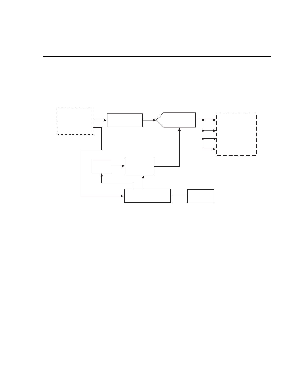
Distortion analog circuitry
Refer to Figure 4-5 for the following discussion on distortion analog circuitry.
Figure 4-5
Distortion analog circuitry block diagram
Troubleshooting 4-15
Analog
Circuitry
(See Figure 4-3)
ADC Converter
U311
Distortion
Digital
Circuitry
(See Figure 4-4)
EEPROM
U315
OSC
Y301
Amplifier Filter
U309, U310
ADC Clock
Generator
U325
FPGA U314
Amplifier filter
The buffered and scaled AC waveform from the analog circuitry (Figure 4-3) is fed to U309
and U310. U309 and U310 form an amplifier, antialiasing filter, and DC shifting circuit to condition the AC waveform for the distortion measurement ADC converter.
ADC converter
The distortion measurement circuitry uses a separate ADC converter from the rest of the
DMM measurements (see U165 in Figure 4-3). This ADC is a high-speed, high-resolution, lowdistortion sigma delta type. The ADC digital output is sent to the DSP through opto-isolators
shown in Figure 4-5.
ADC clock
Y301 is a fixed frequency clock that forms the input to U325, an adjustable frequenc y clock
generator. The output of this generator clocks the ADC, setting the acquisition rate. The clock
generator frequency is set by the microprocessor and is communicated through U314, the
FPGA. The FPGA, U314, is configured by U315, an EEPROM, upon power-up.
Page 79

4-16 Troubleshooting
Sine generator circuitry
Refer to Figure 4-6 for the following discussion on the sine generator circuitry.
Figure 4-6
Sine generator circuitry block diagram
OSC
Sine Generator
U301
Distortion Digital Circuitry
(see Figure 4-4)
Attenuator
U303, U334
U335
FPGA
Inv-Sine/pulse
Filter
U307
EEPROM
-1
Comparator
+1
U305
U306
U307
U308
K301
50/600 Ohm
Inv Sine/
Pulse
Out
Source
Output
Sine generator
Y302 is a fixed frequency clock that forms the input to U301, the adjustable frequency sine
wave generator. The sine wave generator' s frequency is set by the microprocessor through the
FPGA, U334, and the opto-isolators U304, U320, and U321.
Attenuator
U303, U334, U335, and U302 form the adjustable attenuator that adjusts the sine wav e output
amplitude. The output amplitude is set by the microprocessor through the FPGA, U334, and the
opto-isolators U304, U320, and U321.
Page 80

Ω
Troubleshooting 4-17
Filter
U307, U336, and U337 form a low pass filter with a software-selectable cutoff frequency.
This filter is used to reduce spurious noise in the sine wave output. The filter cutof f frequency is
set by the microprocessor through the FPGA, U334, and opto-isolators U304, U320, and U321.
Outputs
The Model 2015 has two outputs. U305, U306, U307, and U308 form the main sine wave
output stage.
The secondary output may be either an inverted sine wave of the same magnitude and frequency as the main sine wave output, or a 5V pulse output of the same frequency as the main
sine wave. One IC is a comparator that squares up the main sine w ave output. Another IC selects
whether the sinewave or the comparator is fed to the output.
K301 selects between either 50
or 600 Ω output impedance.
Page 81

4-18 Troubleshooting
T roubleshooting
Troubleshooting information for the v arious circuits is summarized below . See Principles of
operation for circuit theory.
Display board checks
If the front panel DISP test indicates that there is a problem on the display board, use Table
4-2.
Table 4-2
Display board checks
Step Item/component Required condition Remarks
1
2
3
4
5
6
7
Front panel DISP test.
P1005, PIN 5
P1005, PIN 9
U401, PIN 1
U401, PIN43
U401, PIN 32
U401, PIN 33
Verify that all segments operate.
+5V ±5%
+37V ±5%
Goes low briefly on power up,
then goes high.
4MHz square wave.
Pulse train every 1msec.
Brief pulse train when front
panel key is pressed.
Use front panel display test.
Digital +5V supply.
Display +37V supply.
Microcontroller RESET.
Controller 4MHz clock.
Control from main processor.
Key down data sent to main
processor.
Page 82

Power supply checks
Power supply problems can be checked out using Table 4-3.
Table 4-3
Power supply checks
Step Item/component Required condition Remarks
Troubleshooting 4-19
1
2
3
4
5
6
7
8
9
10
11
12
Line fuse
Line voltage
Line power
U144, pin 2
U101, pin 7
U125, pin 3
U119, pin 3
U124, pin 3
U331, pin 2
U348, pin 3
U349, pin 3
U350, pin 3
Check continuity.
120V/240V as required.
Plugged into live receptacle,
power on.
+5V ±5%
+37V ±5%
+15V ±5%
-15V ±5%
+5V ±5%
+5V, ±3%
+15V, ±5%
-15V, ±5%
+5V, ±5%
Remove to check.
Check power module position.
Check for correct power-up
sequence.
+5VD, referenced to Common D.
+37V, referenced to Common D.
+15V, referenced to Common A.
-15V, referenced to Common A.
+5VRL, referenced to Common A.
+5VD2, referenced to Common D.
+15VA, referenced to Common F.
-15VA, referenced to Common F.
+5VA, referenced to Common F.
Page 83

4-20 Troubleshooting
Digital circuitry checks
Digital circuit problems can be checked out using Table 4-4.
Table 4-4
Digital circuitry checks
Step Item/component Required condition Remarks
1
2
3
4
5
6
7
8
9
10
11
12
13
14
15
16
17
Power-on test
U152 pin 14
U152 pin 28
U135 pin 48
U135, lines A1-A23
U135, lines D1-D15
U135 pin 44
U159 pin 13
U159 pin 14
U158 pins 34-42
U158 pins 26-31
U158 pin 24
U158 pin 25
U135 pin 84
U135 pin 91
U135 pin 90
U135 pin 89
RAM OK, ROM OK.
Digital common.
+5V
Low on power-up, then goes
high.
Check for stuck bits.
Check for stuck bits.
14.7456MHz
Pulse train during RS-232 I/O.
Pulse train during RS-232 I/O.
Pulse train during
IEEE-488
I/O.
Pulses during IEEE-488 I/O.
Low with remote enabled.
Low during interface clear.
Pulse train.
Pulse train.
Pulse train.
Pulse train.
Verify that RAM and ROM are
functional.
All signals referenced to digital
common.
Digital logic supply.
MPU RESET line.
MPU address bus.
MPU data bus.
MPU clock.
RS-232 RX line.
RS-232 TX line.
IEEE-488 data bus.
IEEE-488 command lines.
IEEE-488 REN line.
IEEE-488 IFC line.
ADRXB
ADTX
ADCLK
ADTS
Page 84

Troubleshooting 4-21
Analog signal switching states
Tables 4-5 through 4-11 provide switching states of the various relays, FETs, and analog
switches for the basic measurement functions and ranges. These tables can be used to assist in
tracing an analog signal from the input to the A/D multiplexer.
Table 4-5
DCV signal switching
Range Q101 Q102 Q114 Q136 Q109 K101* Q113 Q105 Q104 Q108 Q121
100mV
1V
10V
100V
1000V
* K101 set states:
Table 4-6
ACV and FREQ signal switching
ON
ON
ON
OFF
OFF
ON
ON
ON
OFF
OFF
OFF
OFF
OFF
ON
ON
Pin 8 switched to Pin 7
Pin 3 switched to Pin 4
OFF
OFF
OFF
ON
ON
Range Q101 Q102 K101* K102*
100mV
1V
10V
100V
750V
* K101 and K102 reset states:
ON
ON
ON
ON
ON
ON
ON
ON
ON
ON
RESET
RESET
RESET
RESET
RESET
K101 and K102 set states:
RESET
RESET
SET
SET
SET
Pin 8 switched to Pin 9
Pin 3 switched to Pin 2
Pin 8 switched to Pin 7
Pin 3 switched to Pin 4
U103
pin 8
ON
ON
OFF
OFF
OFF
OFF
OFF
OFF
OFF
OFF
U103
pin 9
ON
ON
OFF
OFF
OFF
SET
SET
SET
SET
SET
U105
pin 9
OFF
OFF
ON
ON
ON
OFF
OFF
OFF
OFF
OFF
U105
pin 8
OFF
OFF
OFF
OFF
ON
OFF
OFF
OFF
OFF
OFF
U103
pin 16
OFF
ON
OFF
ON
OFF
ON
ON
ON
OFF
OFF
U103
pin 1
ON
OFF
ON
OFF
OFF
OFF
OFF
OFF
ON
ON
U105
pin 1
ON
OFF
ON
OFF
OFF
ON
ON
ON
ON
ON
U111
pin 16
OFF
OFF
OFF
OFF
OFF
Page 85

4-22 Troubleshooting
Table 4-7
Ω
2 signal switching
Range Q101 Q102 Q114 Q136 Q109 K101* K102* Q113 Q105 Q104 Q108 Q121
1k Ω
1M
100 Ω
10k Ω
100k Ω
10MΩ
100MΩ
* K101 set states:
Table 4-8
Ω
ON
ON
ON
ON
Ω
ON
ON
ON
K102 reset states:
4 signal switching
ON
ON
ON
ON
ON
ON
ON
OFF
OFF
OFF
OFF
OFF
OFF
OFF
OFF
OFF
OFF
OFF
OFF
OFF
OFF
Pin 8 switched to Pin 7
Pin 3 switched to Pin 4
Pin 8 switched to Pin 9
Pin 3 switched to Pin 2
OFF
OFF
OFF
OFF
OFF
ON
ON
SET
SET
SET
SET
SET
SET
SET
RESET
RESET
RESET
RESET
RESET
RESET
RESET
OFF
OFF
OFF
OFF
OFF
OFF
OFF
ON
ON
ON
ON
ON
ON
ON
OFF
OFF
OFF
OFF
OFF
OFF
OFF
OFF
OFF
OFF
OFF
OFF
OFF
OFF
ON
ON
ON
ON
ON
ON
ON
Range Q101 Q102 Q114 Q136 Q109 K101* Q113 Q105 Q104 Q108 Q121
100Ω
1kΩ
10kΩ
100kΩ
1MΩ
10MΩ
100MΩ
ON
ON
ON
ON
ON
ON
ON
ON
ON
ON
ON
ON
ON
ON
OFF
OFF
OFF
OFF
OFF
OFF
OFF
OFF
OFF
OFF
OFF
OFF
OFF
OFF
OFF
OFF
OFF
OFF
OFF
ON
ON
SET
SET
SET
SET
SET
SET
SET
ON
ON
ON
ON
ON
OFF
OFF
OFF
OFF
OFF
OFF
OFF
ON
ON
OFF
OFF
OFF
OFF
OFF
OFF
OFF
OFF
OFF
OFF
OFF
OFF
OFF
OFF
ON
ON
ON
ON
ON
ON
ON
*K101 set states:
Table 4-9
Ω
2/
Ω
4 reference switching
Pin 8 switched to Pin 7
Pin 3 switched to Pin 4
Range U133/0.7 U133/7V Q123 Q125 Q124 Q126 Q120
100Ω
1kΩ
10kΩ
100kΩ
1MΩ
10MΩ
100MΩ
OFF
OFF
OFF
ON
ON
OFF
OFF
ON
ON
ON
OFF
OFF
ON
ON
ON
ON
OFF
OFF
OFF
OFF
OFF
ON
ON
OFF
OFF
OFF
OFF
OFF
OFF
OFF
ON
ON
ON
ON
ON
OFF
OFF
ON
ON
ON
ON
ON
ON
ON
ON
ON
ON
OFF
OFF
Page 86

Table 4-10
DCA signal switching
Range K103
Troubleshooting 4-23
10mA
100mA
1A
3A
Table 4-11
ACA signal switching
Range K103
1A
3A
Table 4-12
DCV signal multiplexing and gain
Range
ON
OFF
OFF
OFF
U105
pin 16
OFF
OFFONON
T ables 4-12 through 4-16 can be used to trace the analog signal through the A/D multiplexer
(U163) to the final amplifier stage. These tables show the MUX lines (S3, S4, S6, S7) that are
selected for measurement during the SIGNAL phase of the multiplexing cycle. Also included
are switching states of analog switches (U129) that set up the gain for the final amplifier stage
(U166).
Signal
(U163)
U105
pin 1
ON
ON
U129
pin 1
U111
pin 16
OFFONOFF
U129
pin 8
U129
pin 9
U105
pin 8
OFF
U103
pin 16
OFF
OFF
Gain
(U166)
U103
pin 1
OFF
OFF
100mV
1V
10V
100V
1000V
Table 4-13
ACV and ACA signal multiplexing and gain
Range
S4
S4
S4
S4
S4
Signal
(U163)
OFF
OFF
ON
OFF
ON
U129
pin 1
OFF
ON
OFF
ON
OFF
U129
pin 8
ON
OFF
OFF
OFF
OFF
U129
pin 9
All S3 ON OFF OFF ×1
×100
×10
×1
×10
×1
Gain
(U166)
Page 87

4-24 Troubleshooting
Table 4-14
DCA signal multiplexing and gain
Signal
Range
10mA
100mA
1A
3A
Table 4-15
Ω
2 signal multiplexing and gain
(U163)
S6
S6
S6
S6
Signal
Range
100Ω
1kΩ
10kΩ
100kΩ
1MΩ
10MΩ
100MΩ
Table 4-16
Ω
4 signal multiplexing and gain
(U163)
S4
S4
S4
S4
S4
S4
S4
U129
pin 1
OFF
OFF
OFF
OFF
U129
pin 1
OFF
OFF
OFF
OFF
ON
ON
ON
U129
pin 8
OFF
OFF
OFF
ON
U129
pin 8
OFF
ON
ON
ON
OFF
OFF
OFF
U129
pin 9
ON
ON
ON
OFF
U129
pin 9
ON
OFF
OFF
OFF
OFF
OFF
OFF
Gain
(U166)
×100
×100
×100
×10
Gain
(U166)
×100
×10
×10
×10
×1
×1
×1
Range
100Ω
1kΩ
10kΩ
100kΩ
1MΩ
10MΩ
100MΩ
Signal
(U163)
S4 then S7
S4 then S7
S4 then S7
S4 then S7
S4 then S7
S4 then S7
S4 then S7
U129
pin 1
OFF
OFF
OFF
OFF
ON
ON
ON
U129
pin 8
OFF
ON
ON
ON
OFF
OFF
OFF
U129
pin 9
ON
OFF
OFF
OFF
OFF
OFF
OFF
Gain
(U166)
×100
×10
×10
×10
×1
×1
×1
Page 88

Troubleshooting 4-25
Figure 4-3 provides a block diagram of the analog circuitry. Table 4-17 shows where the various switching devices are located in the block diagram.
Table 4-17
Switching device locations
Switching devices Analog circuit section (see Figure 4-3)
Q101, Q102
Q114, Q136, Q109
K101, Q113, Q105, Q104, Q108
Q121
K102, U103, U105, U111
U133, Q120, Q123, Q124, Q125, Q126
K103
U129, U163
SSP (Solid State Protection)
DCV Divider
DCV and Ohms Switching
Sense LO
AC switching and Gain
Ohms I-Source
Current Shunts
A/D Mux and Gain
Page 89

5
Disassembly
Page 90

5-2 Disassembly
Introduction
This section explains how to handle, clean, and disassemble the Model 2015 Multimeter. Dis-
assembly drawings are located at the end of this section.
Page 91

Disassembly 5-3
Handling and cleaning
T o avoid contaminating PC board traces with body oil or other foreign matter, avoid touching
the PC board traces while you are repairing the instrument. Motherboard areas covered by the
shield have high-impedance devices or sensitive circuitry where contamination could cause
degraded performance.
Handling PC boards
Observe the following precautions when handling PC boards:
• Wear cotton gloves.
• Only handle PC boards by the edges and shields.
• Do not touch any board traces or components not associated with repair.
• Do not touch areas adjacent to electrical contacts.
• Use dry nitrogen gas to clean dust off PC boards.
Solder repairs
Observe the following precautions when soldering a circuit board:
• Use an OA-based (organic activated) flux, and take care not to spread the flux to other
areas of the circuit board.
• Remove the flux from the work area when you have finished the repair by using pure
water with clean, foam-tipped swabs or a clean, soft brush.
• Once you have remov ed the flux, swab only the repair area with methanol, then blo w dry
the board with dry nitrogen gas.
• After cleaning, allow the board to dry in a 50°C, low-humidity environment for several
hours.
Page 92

5-4 Disassembly
Static sensitive devices
you or your clothing may be sufficient to destroy these de vices if the y are not handled properly.
Use the following precautions to avoid damaging them:
CAUTION Many CMOS devices are installed in the Model 2015. Handle all semicon-
CMOS devices operate at very high impedance le vels. Therefore, an y static that builds up on
ductor devices as being static sensitive.
• Transport and handle ICs only in containers specially designed to prevent static buildup. Typically, you will receive these parts in anti-static containers made of plastic or
foam. Keep these devices in their original containers until ready for installation.
• Remove the devices from their protective containers only at a properly grounded work
station. Also, ground yourself with a suitable wrist strap.
• Handle the devices only by the body; do not touch the pins.
• Ground any printed circuit board into which a semiconductor device is to be inserted to
the bench or table.
• Use only anti-static type desoldering tools.
• Use only grounded-tip solder irons.
• Once the device is installed in the PC board, it is normally adequately protected, and you
can handle the boards normally.
Page 93

Assembly drawings
Use the following assembly drawings to assist you as you disassemble and re-assemble the
Model 2015. Also, refer to these drawings for information about the Keithley part numbers of
most mechanical parts in the unit. The drawings are located at the end of this section of the
manual.
• Front Panel Assembly — 2015-040
• Chassis/Transformer Power Module Assembly — 2015-050
• Front Panel/Chassis Assembly — 2015-051
• Chassis Assembly — 2015-052, 2015-053
• Final Inspection — 2015-080
Disassembly 5-5
Page 94

5-6 Disassembly
Disassembly procedures
Case cover removal
Follow the steps below to remove the case cover to gain access to internal parts.
WARNING Before removing the case cover, disconnect the line cord and any test leads
from the instrument.
1. Remove Handle — The handle serves as an adjustable tilt-bail. Adjust its position by
gently pulling it away from the sides of the instrument case and swinging it up or do wn.
To remove the handle, swing the handle below the bottom surface of the case and back
until the orientation arrows on the handles line up with the orientation arrows on the
mounting ears. W ith the arro ws lined up, pull the ends of the handle a way from the case.
2. Remove Mounting Ears — Remov e the screw that secures each mounting ear . Pull do wn
and out on each mounting ear.
NOTE When re-installing the mounting ears, make sure to mount the right ear to the right
side of the chassis, and the left ear to the left side of the chassis. Eac h ear is marked
“RIGHT” or “LEFT” on its inside surface.
3. Remove Rear Bezel — To remove the rear bezel, loosen the two captive screws that secure the rear bezel to the chassis. Pull the bezel away from the case.
4. Removing Grounding Screws — Remov e the two grounding scre ws that secure the case
to the chassis. They are located on the bottom of the case at the back.
5. Remove Cover — T o remove the case, grasp the front bezel of the instrument, and carefully slide the chassis forward. Slide the chassis out of the metal case.
NOTE To gain access to the components under the DMM board shield, remove the shield,
which is secured to the DMM board by a single screw.
DMM board removal
Perform the following steps to remove the DMM (106) board. This procedure assumes that
the case cover is already removed.
1. Remove the IEEE-488 and RS-232 fasteners.
The IEEE-488 and the RS-232 connectors each have two nuts that secure the connectors
to the rear panel. Remove these nuts.
2. Remove the front/rear switch rod.
At the switch, place the edge of a flat-blade screw driver in the notch on the pushrod.
Gently twist the screw driver while pulling the rod from the shaft.
Page 95

Disassembly 5-7
3. Disconnect the front and rear input terminals.
You must disconnect these input terminal connections for both the front and rear inputs:
• INPUT HI and LO
• SENSE HI and LO
• AMPS
Remove all the connections except the front AMPS connection by pulling the wires off
the pin connectors. T o remo ve the front panel AMPS input wire (white), first remove the
AMPS fuse holder, then use needle-nose pliers to grasp the AMPS wire near fuse housing. Push the wire forward and down to snap the spring out of the fuse housing. Carefully
pull the spring and contact tip out of the housing.
4. Unplug cables:
• Unplug the display board ribbon cable from connector J1014.
• Unplug the transformer cables from connectors J1016 and J1015.
• Unplug the OPTION SLOT ribbon cable from connector J1017.
5. Remove the fastening screw that secures the DMM board to the chassis. One of these
screws is located along the left side of the unit tow ards the rear , and it also secures U114.
The other screw is located at the right front of the chassis near the front/rear switch,
S101.
During re-assembly, replace the board, and start the IEEE-488 and RS-232 connector
nuts and the mounting screw. Tighten all the fasteners once they are all in place and the
board is correctly aligned.
6. Remove the DMM board, which is held in place by edge guides on each side, by sliding
it forward until the board edges clear the guides. Carefully pull the DMM board from the
chassis.
DSP board removal
Perform the following steps to remove the DSP (136) board. This procedure assumes that the
case cover and the DMM board have been removed.
1. Remove the nuts from the two BNC jacks on the rear panel.
2. Unplug cables:
• Unplug the power entry module cable, J1021.
• Unplug the transformer primary connections, J1018 and J1019.
• Unplug the transformer cable from J1020.
• Unplug the DMM board connectors, J1022, J1024, and J1026.
• Unplug the transformer cable, J1031.
3. Remove all seven screws that secure the DSP board to the chassis.
4. Slide the board toward the front of the chassis until the BNC jacks ha ve cleared the chassis and the board is clear of the guide pins, then remove the board.
During re-assembly, replace the board by lining up the guide pins over the slots, then
slide the board toward the rear. Loosely install all screws, then install and tighten the
BNC jack nuts. Tighten all screws.
Page 96

5-8 Disassembly
Front panel disassembly
NOTE You must first remove the case cover, the front/rear input switch, and the front input
Use the following procedures to remov e the display board and/or the pushbutton switch pad:
terminal wires as described earlier in this section.
1. Unplug the display board ribbon cable from connector J1014.
2. Remove the front panel assembly.
This assembly has four retaining clips that snap onto the chassis over four pem nut studs.
Two retaining clips are located on each side of the front panel. Pull the retaining clips
outward and, at the same time, pull the front panel assembly forward until it separates
from the chassis.
3. Using a thin-bladed screw driv er , pry the plastic PC board stop (located at the bottom of
the display board) until the bar separates from the casing. Pull the display board from the
front panel.
4. Remove the switch pad by pulling it from the front panel.
Removing power components
The following procedures to remove the po wer transformer and/or po wer module require that
the case cover and motherboard be removed, as previously explained.
Power transformer removal
Perform the following steps to remove the power transformer:
1. Remove the DMM board.
2. Unplug the transformer wires that attach to the DSP board:
• For TR-332, unplug J1018 and J1020.
• For TR-328, unplug J1019 and J1031.
3. Remove the two nuts that secure the transformer to the bottom of the chassis.
4. Pull the black ground wire off the threaded stud, and remov e the power transformer from
the chassis.
Power module removal
Perform the following steps to remove the power module:
1. Remove the DMM board.
2. Unplug connector J1021 from the DSP board.
3. Disconnect the power module's ground wire. This green and yellow wire connects to a
threaded stud on the chassis with a kep nut.
4. Squeeze the latches on either side of the power module while pushing the module from
the access hole.
Page 97

Instrument reassembly
Reassemble the instrument by reversing the pre vious disassembly procedures. Make sure that
all parts are properly seated and secured, and that all connections are properly made. To ensure
proper operation, replace and securely fasten the shield.
WARNING To ensure continued protection against electrical shock, verify that power
line ground (green and yellow wire attached to the power module) and the
power transformer ground (black wire) are connected to the chassis. When
installing the power transformer, be sure to re-connect the black ground
wire to the mounting stud on bottom of the chassis. Be sure to install the
bottom case screws to assure a good case-to-chassis ground connection.
Disassembly 5-9
Input terminal wire connections
During reassembly, use the information in Table 5-1 to connect input terminal wires.
Table 5-1
Input terminal wire colors
Input terminal Front wire color Rear wire color
INPUT HI
INPUT LO
SENSE HI
SENSE LO
AMPS
Red
Black
Yellow
Gray
White
Power module wire connections
Use the information in T able 5-2 and DETAIL B of drawing 2015-050 to connect power module wires.
Table 5-2
Power module wire colors
Location Wire color
White/Red
White/Black
White/Yellow
White/Gray
—
Top wire
Right top
Right bottom
Left top
Left bottom
Gray
Violet
White
Red
Blue
Page 98

5-10 Disassembly
Changing trigger link lines
The Model 2015 uses two lines of the T rigger Link rear panel connector as External Trigger
(EXT TRIG) input and Voltmeter Complete (VMC) output. At the factory, line 1 is configured
as VMC and line 2 as EXT TRIG.
NOTE Line 1, 3, or 5 of the T rigger Link can be confi gur ed as VMC, while line 2, 4, or 6 can
be configured as EXT TRIG.
You can change trigger link line configurations by moving the position of resistors inside the
unit. Perform the following steps to change trigger link lines:
WARNING Make sure the instrument is disconnected from the power line and other
equipment before performing the following procedure.
1. Remove the cover from the instrument as explained in Case cover removal.
2. The resistors used to select the trigger link lines are located next to the Trigger Link
connector as shown in Figure 5-1. The “resistors” are actually solder beads that bridge
PC-board pads. If the factory default lines are selected, the solder beads will be located
at R270 (line 2, EXT TRIG) and R267 (line 1, VMC).
3. To change a trigger link line:
• Use a soldering iron and solder sucker to remove the appropriate solder bead.
• Using a solder with OA-based flux, apply a solder bead to the appropriate resistor
• Replace the cover on the instrument.
Figure 5-1
Trigger link line connections
Trigger Link Lines
Line 1 = VMC (R267)
Line 2 = EXT TRIG (R270)
Line 3 = VMC (R266)
Line 4 = EXT TRIG (R268)
Line 5 = VMC (R265)
Line 6 = EXT TRIG (R269)
location.
DMM Board
(View from top)
R270
R269
R268
R270
R269
R268
Rear Panel
Solder Bead
Trigger
Link
Connector
(Factory Default Configured)
Page 99

Main CPU firmware replacement
Changing the firmware may be necessary as upgrades become available. The firmware revision levels for the main and front panel CPUs are displayed during the po wer-on sequence. (The
main firmware revision level is displayed on the left; the front panel firmware revision level is
displayed on the right.) For example: REV: A01 A02 indicates a main firmware revision level
of A01 and a front panel firmware revision level of A02.
The firmware for the main CPU is located in the EPROMs U156 (EVEN) and U157 (ODD),
leadless ICs that resides in chip carriers on the PC board. To replace the CPU firmware, do the
following:
WARNING Disconnect the instrument from the power lines, and remove the test leads
before changing the firmware.
Disassembly 5-11
1. Remove the case cover as described earlier in this section.
2. Locate U156 EVEN and U157 ODD (EPROMs) on the DMM (106) board. They are the
only devices installed in chip carriers (sockets).
CAUTION EPROMs U156 and U157 are static-sensitive devices. Be sure to follow the
handling precautions explained in Static sensitive devices.
3. Using an appropriate chip extractor, remove U156 from its chip carrier.
4. Position the new U156 EPROM on the appropriate chip carrier. Make sure the notched
corner of the chip is aligned with the notch in the chip carrier.
NOTE Be sure to install the correct EPROMs at the ODD and EVEN locations. The instru-
ment will not function if the EPROMs are installed in the wrong sockets.
5. With the EPROM properly positioned, push down on the chip until it completely seats
into the chip carrier.
6. Repeat steps 3 through 5 for EPROM U157.
7. After installation, make sure the instrument powers up normally before replacing the
cover.
Page 100

5-12 Disassembly
 Loading...