

Page 1

Model 2010
Multimeter
Service Manual
Contains Calibrating and Servicing Information
Page 2

W ARRANTY
Keithley Instruments, Inc. warrants this product to be free from defects in material and workmanship for a
period of 3 years from date of shipment.
Keithley Instruments, Inc. warrants the following items for 90 days from the date of shipment: probes,
cables, rechargeable batteries, diskettes, and documentation.
During the warranty period, we will, at our option, either repair or replace any product that proves to be
defective.
T o e xercise this w arranty, write or call your local K eithley representati v e, or contact K eithle y headquarters in
Cleveland, Ohio. You will be given prompt assistance and return instructions. Send the product, transportation prepaid, to the indicated service facility. Repairs will be made and the product returned, transportation
prepaid. Repaired or replaced products are warranted for the balance of the original warranty period, or at
least 90 days.
LIMIT A TION OF W ARRANTY
This warranty does not apply to defects resulting from product modification without Keithley’s express written consent, or misuse of any product or part. This warranty also does not apply to fuses, software, nonrechargeable batteries, damage from battery leakage, or problems arising from normal wear or failure to follow instructions.
THIS WARRANTY IS IN LIEU OF ALL OTHER WARRANTIES, EXPRESSED OR IMPLIED, INCLUDING ANY IMPLIED WARRANTY OF MERCHANTABILITY OR FITNESS FOR A PARTICULAR USE.
THE REMEDIES PROVIDED HEREIN ARE B UYER’S SOLE AND EXCLUSIVE REMEDIES.
NEITHER KEITHLEY INSTRUMENTS, INC. NOR ANY OF ITS EMPLOYEES SHALL BE LIABLE
FOR ANY DIRECT, INDIRECT, SPECIAL, INCIDENTAL OR CONSEQUENTIAL DAMAGES ARISING OUT OF THE USE OF ITS INSTRUMENTS AND SOFTWARE EVEN IF KEITHLEY INSTRUMENTS, INC., HAS BEEN ADVISED IN ADVANCE OF THE POSSIBILITY OF SUCH DAMAGES.
SUCH EXCLUDED DAMAGES SHALL INCLUDE, BUT ARE NOT LIMITED TO: COSTS OF
REMOVAL AND INSTALLATION, LOSSES SUSTAINED AS THE RESULT OF INJURY TO ANY PERSON, OR DAMAGE TO PROPERTY.
Keithley Instruments, Inc. • 28775 Aurora Road • Cleveland, OH 44139 • 440-248-0400 • Fax: 440-248-6168 • http://www.k eithley.com
BELGIUM: Keithley Instruments B.V. Bergensesteenweg 709 • B-1600 Sint-Pieters-Leeuw • 02/363 00 40 • Fax: 02/363 00 64
CHINA: Keithley Instruments China Y uan Chen Xin Building, Room 705 • 12 Yumin Road, Dewai, Madian • Beijing 100029 • 8610-62022886 • Fax: 8610-62022892
FRANCE: Keithley Instruments Sarl B.P. 60 • 3, allée des Garays • 91122 Palaiseau Cédex • 01 64 53 20 20 • Fax: 01 60 11 77 26
GERMANY: Keithley Instruments GmbH Landsberger Strasse 65 • D-82110 Germering • 089/84 93 07-40 • Fax: 089/84 93 07-34
GREAT BRITAIN: Keithley Instruments Ltd The Minster • 58 Portman Road • Reading, Berkshire RG30 1EA • 0118-9 57 56 66 • Fax: 0118-9 59 64 69
INDIA: Keithley Instruments GmbH Flat 2B, WILOCRISSA • 14, Rest House Crescent • Bangalore 560 001 • 91-80-509-1320/21 • Fax: 91-80-509-1322
ITALY: Keithley Instruments s.r.l. Viale S. Gimignano, 38 • 20146 Milano • 02/48 30 30 08 • Fax: 02/48 30 22 74
NETHERLANDS: Keithley Instruments B.V. Postbus 559 • 4200 AN Gorinchem • 0183-635333 • Fax: 0183-630821
SWITZERLAND: Keithley Instruments SA Kriesbachstrasse 4 • 8600 Dübendorf • 01-821 94 44 • Fax: 01-820 30 81
TAIWAN: Keithley Instruments Taiwan 1 Fl. 85 Po Ai Street • Hsinchu, Taiwan, R.O.C. • 886-3572-9077• Fax: 886-3572-9031
6/99
Page 3

Model 2010 Multimeter
Service Manual
©1996, Keithley Instruments, Inc.
All rights reserved.
Cleveland, Ohio, U.S.A.
Third Printing, September 1999
Document Number: 2010-902-01 Rev. C
Page 4

Manual Print History
The print history shown below lists the printing dates of all Revisions and Addenda created
for this manual. The Revision Le vel letter increases alphabetically as the manual under goes subsequent updates. Addenda, which are released between Revisions, contain important change information that the user should incorporate immediately into the manual. Addenda are numbered
sequentially . When a new Re vision is created, all Addenda associated with the previous Re vision
of the manual are incorporated into the new Revision of the manual. Each ne w Revision includes
a revised copy of this print history page.
Revision A (Document Number 2010-902-01)............................................................January 1996
Revision B (Document Number 2010-902-01)................................................................. June 1999
Addendum B (Document Number 2010-902-02).................................................... September 1999
Revision C (Document Number 2010-902-01)....................................................... September 1999
All Keithley product names are trademarks or registered trademarks of Keithley Instruments, Inc.
Other brand names are trademarks or registered trademarks of their respective holders.
Page 5

Safety Precautions
The following safety precautions should be observed before using this product and any associated instrumentation. Although some instruments and accessories would normally be used with non-hazardous v oltages, there
are situations where hazardous conditions may be present.
This product is intended for use by qualified personnel who recognize shock hazards and are familiar with the
safety precautions required to avoid possible injury. Read the operating information carefully before using the
product.
The types of product users are:
Responsible body is the individual or group responsible for the use and maintenance of equipment, for ensuring
that the equipment is operated within its specifications and operating limits, and for ensuring that operators are
adequately trained.
Operators use the product for its intended function. They must be trained in electrical safety procedures and
proper use of the instrument. They must be protected from electric shock and contact with hazardous live circuits.
Maintenance personnel perform routine procedures on the product to keep it operating, for example, setting
the line voltage or replacing consumable materials. Maintenance procedures are described in the manual. The
procedures explicitly state if the operator may perform them. Otherwise, they should be performed only by service personnel.
Service personnel are trained to work on live circuits, and perform safe installations and repairs of products.
Only properly trained service personnel may perform installation and service procedures.
Exercise extreme caution when a shock hazard is present. Lethal voltage may be present on cable connector
jacks or test fixtures. The American National Standards Institute (ANSI) states that a shock hazard exists when
voltage levels greater than 30V RMS, 42.4V peak, or 60VDC are present.
expect that hazardous voltage is present in any unknown circuit before measuring.
Users of this product must be protected from electric shock at all times. The responsible body must ensure that
users are prevented access and/or insulated from every connection point. In some cases, connections must be
exposed to potential human contact. Product users in these circumstances must be trained to protect themselves
from the risk of electric shock. If the circuit is capable of operating at or above 1000 volts,
of the circuit may be exposed.
As described in the International Electrotechnical Commission (IEC) Standard IEC 664, digital multimeter
measuring circuits (e.g., Keithley Models 175A, 199, 2000, 2001, 2002, and 2010) are Installation Category II.
All other instruments’ signal terminals are Installation Category I and must not be connected to mains.
Do not connect switching cards directly to unlimited power circuits. They are intended to be used with impedance limited sources. NEVER connect switching cards directly to AC mains. When connecting sources to
switching cards, install protective devices to limit fault current and voltage to the card.
Before operating an instrument, make sure the line cord is connected to a properly grounded power receptacle.
Inspect the connecting cables, test leads, and jumpers for possible wear, cracks, or breaks before each use.
For maximum safety, do not touch the product, test cables, or any other instruments while power is applied to
the circuit under test. ALWAYS remove power from the entire test system and discharge an y capacitors before:
connecting or disconnecting cables or jumpers, installing or removing switching cards, or making internal
changes, such as installing or removing jumpers.
A good safety practice is to
no conductive part
Do not touch any object that could provide a current path to the common side of the circuit under test or power
line (earth) ground. Always make measurements with dry hands while standing on a dry, insulated surface capable of withstanding the voltage being measured.
Page 6

The instrument and accessories must be used in accordance with its specifications and operating instructions or
the safety of the equipment may be impaired.
Do not exceed the maximum signal levels of the instruments and accessories, as defined in the specifications
and operating information, and as shown on the instrument or test fixture panels, or switching card.
When fuses are used in a product, replace with same type and rating for continued protection against fire hazard.
Chassis connections must only be used as shield connections for measuring circuits, NOT as safety earth ground
connections.
If you are using a test fixture, keep the lid closed while power is applied to the device under test. Safe operation
requires the use of a lid interlock.
If a screw is present, connect it to safety earth ground using the wire recommended in the user documentation.
!
The symbol on an instrument indicates that the user should refer to the operating instructions located in
the manual.
The symbol on an instrument shows that it can source or measure 1000 volts or more, including the combined effect of normal and common mode voltages. Use standard safety precautions to avoid personal contact
with these voltages.
The
WARNING heading in a manual explains dangers that might result in personal injury or death. Always
read the associated information very carefully before performing the indicated procedure.
The
CAUTION heading in a manual explains hazards that could damage the instrument. Such damage may
invalidate the warranty.
Instrumentation and accessories shall not be connected to humans.
Before performing any maintenance, disconnect the line cord and all test cables.
To maintain protection from electric shock and fire, replacement components in mains circuits, including the
power transformer, test leads, and input jacks, must be purchased from Keithley Instruments. Standard fuses,
with applicable national safety approvals, may be used if the rating and type are the same. Other components
that are not safety related may be purchased from other suppliers as long as they are equivalent to the original
component. (Note that selected parts should be purchased only through Keithley Instruments to maintain accuracy and functionality of the product.) If you are unsure about the applicability of a replacement component,
call a Keithley Instruments office for information.
T o clean an instrument, use a damp cloth or mild, water based cleaner . Clean the e xterior of the instrument only .
Do not apply cleaner directly to the instrument or allow liquids to enter or spill on the instrument. Products that
consist of a circuit board with no case or chassis (e.g., data acquisition board for installation into a computer)
should never require cleaning if handled according to instructions. If the board becomes contaminated and operation is affected, the board should be returned to the factory for proper cleaning/servicing.
Rev. 2/99
Page 7

T able of Contents
1
Performance Verification
Introduction......................................................................................... 1-2
Verification test requirements.............................................................. 1-3
Performing the verification test procedure..........................................1-6
Verifying DC voltage .......................................................................... 1-7
V erifying A C voltage........................................................................... 1-8
Verifying DC current......................................................................... 1-10
V erifying A C current.........................................................................1-11
Verifying resistance........................................................................... 1-12
Verifying temperature ....................................................................... 1-14
Verifying frequency........................................................................... 1-17
Verifying ratio ................................................................................... 1-18
2
Calibration
Introduction......................................................................................... 2-2
Environmental conditions...................................................................2-3
Calibration considerations................................................................... 2-4
Calibration code..................................................................................2-5
Comprehensive calibration..................................................................2-6
Front panel calibration........................................................................2-8
Remote calibration............................................................................2-16
Manufacturing calibration................................................................. 2-24
Routine Maintenance
3
Introduction......................................................................................... 3-2
Setting the line voltage and replacing the line fuse.............................3-2
Replacing the AMPS fuse................................................................... 3-4
T roubleshooting
4
Introduction......................................................................................... 4-2
Repair considerations.......................................................................... 4-2
Power-on self-test................................................................................4-2
Front panel tests..................................................................................4-3
Principles of operation........................................................................4-4
Troubleshooting................................................................................4-10
Analog signal switching states.......................................................... 4-13
No comm link error........................................................................... 4-18
Page 8

Disassembly
5
Introduction.........................................................................................5-2
Handling and cleaning.........................................................................5-2
Static sensitive devices........................................................................5-3
Assembly drawings .............................................................................5-4
Case cover removal .............................................................................5-5
Changing trigger link lines..................................................................5-6
Motherboard removal..........................................................................5-7
Front panel disassembly......................................................................5-8
Main CPU firmware replacement........................................................5-9
Removing power components...........................................................5-10
Instrument re-assembly .....................................................................5-12
6
Replaceable Parts
Introduction.........................................................................................6-2
Parts lists..............................................................................................6-2
Ordering information...........................................................................6-2
Factory service ....................................................................................6-3
Component layouts..............................................................................6-3
Specifications
A
Accuracy calculations.........................................................................A-7
Calibration Command Reference
B
Introduction........................................................................................B-2
Command summary ........................................................................... B-2
Miscellaneous calibration commands ................................................ B-4
DC calibration commands.................................................................. B-8
AC calibration commands................................................................ B-14
Manufacturing calibration commands.............................................. B-16
Remote error reporting..................................................................... B-18
Detecting calibration step completion.............................................. B-21
Calibration Program
C
Introduction........................................................................................C-2
Computer hardware requirements...................................................... C-2
Software requirements........................................................................ C-2
Calibration equipment........................................................................ C-3
General program instructions............................................................. C-3
Page 9

List of Illustrations
1
Performance Verification
Connections for DC volts verification.................................................1-7
Connections for AC volts verification................................................. 1-8
Connections for DC current verification........................................... 1-10
Connections for AC current verification...........................................1-11
Connections for resistance verification (10 Ω -10M Ω ranges)........... 1-12
Connections for resistance verification (100M Ω range)................... 1-13
Connections for frequency verification.............................................1-17
Verifying ratio ................................................................................... 1-18
2
Calibration
Low-thermal short connections........................................................... 2-9
Calibrator connections for DC volts and ohms portion
of comprehensive calibration........................................................ 2-10
Connections for DC and AC amps comprehensive calibration......... 2-12
Connections for AC volts calibration................................................ 2-13
Synthesizer connections for manufacturing calibration....................2-25
Routine Maintenance
3
Power module......................................................................................3-3
T roubleshooting
4
Power supply block diagram............................................................... 4-5
Digital circuitry block diagram........................................................... 4-7
Analog circuitry block diagram .......................................................... 4-8
5
Disassembly
Trigger link connectors.......................................................................5-6
Page 10

List of T ables
1
Performance Verification
Recommended verification equipment................................................1-4
DCV reading limits .............................................................................1-7
ACV reading limits..............................................................................1-9
DCI limits..........................................................................................1-10
ACI limits..........................................................................................1-11
Limits for resistance verification.......................................................1-13
Thermocouple temperature verification reading limits.....................1-15
Four-wire RTD temperature verification reading limits....................1-16
2
Calibration
Recommended equipment for comprehensive, DC-only,
or AC-only calibration......................................................................2-6
Comprehensive calibration procedures...............................................2-8
DC volts calibration summary...........................................................2-11
Ohms calibration summary ...............................................................2-11
DC current calibration summary.......................................................2-12
AC voltage calibration summary.......................................................2-13
AC current calibration summary.......................................................2-14
DC voltage calibration programming steps.......................................2-18
Resistance calibration programming steps........................................2-19
DC current calibration programming steps.......................................2-20
AC voltage calibration programming steps.......................................2-21
AC current calibration programming steps.......................................2-22
Recommended equipment for manufacturing calibration.................2-24
3
Routine Maintenance
Power line fuse....................................................................................3-3
4
T roubleshooting
Power supply components...................................................................4-4
Display board checks ........................................................................ 4-10
Power supply checks.........................................................................4-11
Digital circuitry checks .....................................................................4-12
DCV signal switching .......................................................................4-13
ACV and FREQ signal switching......................................................4-13
Ω
2 signal switching...........................................................................4-14
Ω 4 signal switching...........................................................................4-14
2/ Ω 4 reference switching...............................................................4-15
Ω
DCA signal switching .......................................................................4-15
Page 11

ACA signal switching........................................................................4-15
DCV signal multiplexing and gain....................................................4-16
ACV and ACA signal multiplexing and gain.....................................4-16
DCA signal multiplexing and gain....................................................4-16
Ω 2 signal multiplexing and gain........................................................4-17
Ω 4 signal multiplexing and gain........................................................4-17
Circuit section locations for switching devices.................................4-17
6
Replaceable Parts
Mother board parts list.........................................................................6-4
Display board parts list......................................................................6-11
Connector board parts list..................................................................6-11
Mechanical parts list..........................................................................6-12
B
Calibration Command Reference
Remote calibration command summary.............................................B-2
DC calibration commands ..................................................................B-8
AC calibration commands ................................................................B-14
Calibration error summary................................................................B-18
Page 12

1
Performance
V erification
Page 13

1-2 Performance Verification
Introduction
Use the procedures in this section to verify that the Model 2010 Multimeter accuracy is within
the limits stated in the instrument’s one-year accuracy specifications. You can perform verification procedures:
• When you first receive the instrument to make sure that it w as not damaged during shipment, and that the unit meets factory specifications.
• If the instrument’s accuracy is questionable.
• Following calibration.
WARNING The information in this section is intended only for qualified service person-
nel. Do not attempt these procedures unless you are qualified to do so.
NOTE
If the instrument is still under warranty and its performance is outside specified limits, contact your Keithle y repr esentative or the factory to determine the corr ect course
of action.
Page 14

Performance Verification 1-3
V erification test requirements
Be sure that you perform the verification tests:
• Under the proper environmental conditions.
• After the specified warm-up period.
• Using the correct line voltage.
• Using the proper calibration equipment.
• Using the specified reading limits.
Environmental conditions
Conduct your performance verification procedures in a test environment that has:
• An ambient temperature of 18-28°C (65-82°F).
• A relative humidity of less than 80% unless otherwise noted.
W arm-up period
Allow the Model 2010 Multimeter to warm up for at least two hours before conducting the
verification procedures.
If the instrument has been subjected to temperature extremes (those outside the ranges stated
above), allow additional time for the instrument’s internal temperature to stabilize. T ypically , allow one extra hour to stabilize a unit that is 10°C (18°F) outside the specifi ed temperature range.
Also, allow the test equipment to warm up for the minimum time specified by the manufacturer.
Line power
The Model 2010 Multimeter requires a line voltage of 100V/120V/220V/240V, ±10% and a
line frequency of 45Hz to 66Hz and 360Hz to 440Hz.
Page 15
1-4 Performance Verification
Recommended test equipment
Table 1-1 summarizes recommended verification equipment. Use the Fluke Model 5700A
Calibrator (or the equivalent) to v erify Model 2010 Multimeter measurement accurac y. You can
use alternate equipment as long as that equipment has specifications at least as good as those
listed in T able 1-1. K eep in mind, ho wev er , that the calibrator will add to the uncertainty of each
measurement. Table 1-1 lists the uncertainties of the recommended Fluke 5700A at each source
value.
Table 1-1
Recommended verification equipment
Fluke 5700A Calibrator:
DC voltage
100mV:±14ppm
1.0V:±7ppm
10V:±5ppm
100V:±7ppm
1000V:±9ppm
Fluke 5725A Amplifier:
AC Voltage, 50kHz: 700V, ±375ppm
Keithley 3930A or 3940 Frequency Synthesizer:
1V RMS, 1kHz, ±5ppm
General Radio 1433-T Precision Decade Resistance Box:
10 Ω -400 Ω , ±0.02%
*1kHz specifications shown. 5725A amplifier required to source 700V at 50kHz.
NOTE: The Fluke 5725A amplifier is necessary only if you wish to verify the 750V AC range at 50kHz. Verification at 220V, 50kHz using only the 5700A calibrator is adequate for most applications.
AC voltage
(1kHz, 50kHz)*
100mV:±200ppm
1.0V:±82ppm
10V:±82ppm
100V:±90ppm
700V:±85ppm
DC current
10mA:±60ppm
100mA:±70ppm
1A:±110ppm
2.2A:±94ppm
AC current
(1kHz)
1A:±690ppm
2.2A:±682ppm
Resistance
10
Ω :±28ppm
100
Ω :±17ppm
1k
Ω :±12ppm
10k
Ω :±11ppm
100k
Ω :±13ppm
1M
Ω :±18ppm
10M
Ω :±37ppm
100M
Ω :±120ppm
Page 16

V erification limits
The verification limits stated in this section have been calculated using only the Model 2010
one-year accuracy specifications. All ranges do not include the verification equipment’s uncertainty. If a particular measurement falls slightly outside the allowable range, recalculate new
limits based on both Model 2010 specifications and pertinent calibration equipment specifications.
Example reading limit calculation
The following is an example of how reading limits have been calculated:
Assume you are testing the 10V DC range using a 10V input value. Using the Model 2010
one-year accuracy specification for 10V DC of ± (24ppm of reading + 4ppm of range), the calculated limits are:
Performance Verification 1-5
Reading limits = 10V ± [(10V
Reading limits = 10V ± (.00024 + .00004)
Reading limits = 10V ± .00028V
Reading limits = 9.99972V to 10.00028V
Calculating resistance reading limits
Resistance reading limits must be recalculated based on the actual calibration resistance values supplied by the equipment manufacturer . Calculations are performed in the same manner as
shown in the preceding example, except you should use the actual calibration resistance values
instead of the nominal values when performing your calculations.
Restoring factory defaults
Before performing the verification procedures, restore the instrument to its factory defaults
as follows:
1. Press SHIFT and then SETUP. The instrument will display the following prompt:
RESTORE: FACT
NOTE Pressing either range key toggles the RESTORE selection between USER and FACT.
2. Select FACT, and then restore the factory default conditions by pressing ENTER.
3. Factory defaults will be set as follows:
Speed: medium
Filter: 10 readings
× 24ppm) + (10V × 4ppm)]
Page 17

1-6 Performance Verification
Performing the verification test procedures
T est summary
Verification test procedures include:
• DC volts
• AC volts
• DC current
• AC current
• Resistance
• Temperature
• Frequency
• Ratio
If the Model 2010 is not within specifications and not under warranty , see the calibration pro-
cedures in Section 2.
T est considerations
When performing the verification procedures:
• Be sure to restore factory defaults as outlined above.
• Restore factory defaults and choose the measurement function to be tested.
• Make sure that the equipment is properly warmed up and connected to the front panel
input jacks. Also mak e sure that the front panel input jacks are selected with the INPUTS
switch.
• Do not use autoranging for any verification tests because autorange hysteresis may cause
the Model 2010 to be on an incorrect range. For each test signal, you must manually set
the correct range for the Model 2010 using the range keys.
• Make sure the calibrator is in operate before you verify each measurement.
• Always let the source signal settle before taking a reading.
• Do not connect test equipment to the Model 2010 through a scanner or other switching
equipment.
W ARNING The maximum common-mode voltage (voltage between INPUT LO and chas-
sis ground) is 500V peak. Exceeding this value may cause a breakdown in insulation, creating a shock hazard. Some of the procedures in this section may
expose you to dangerous voltages. Use standard safety precautions when
such dangerous voltages are encountered to avoid personal injury caused by
electric shock.
Page 18
V erifying DC voltage
Check DC voltage accuracy by applying accurate v oltages from the DC v oltage calibrator to
the Model 2010 INPUT jacks and verifying that the displayed readings fall within specified limits. Follow these steps to verify the DC voltage:
CAUTION Do not exceed 1000V peak between INPUT HI and INPUT LO because in-
strument damage may occur.
1. Connect the Model 2010 HI and LO INPUT jacks to the DC voltage calibrator as sho wn
in Figure 1-1.
NOTE Use shielded, low-thermal connections when testing the 100mV and 1V ranges to
avoid errors caused by noise or thermal ef fects. Connect the shield to the calibr ator’s
output LO terminal.
Performance Verification 1-7
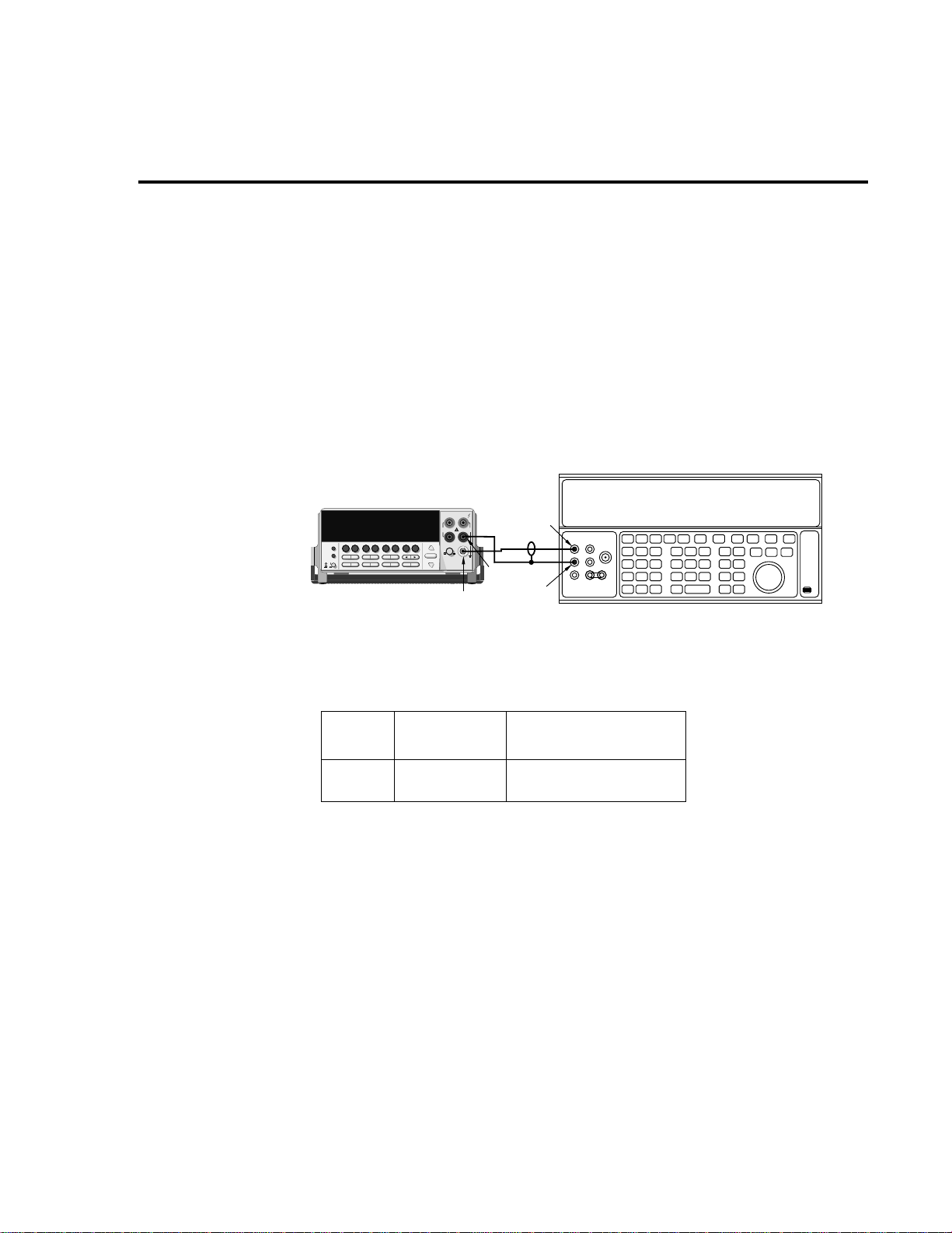
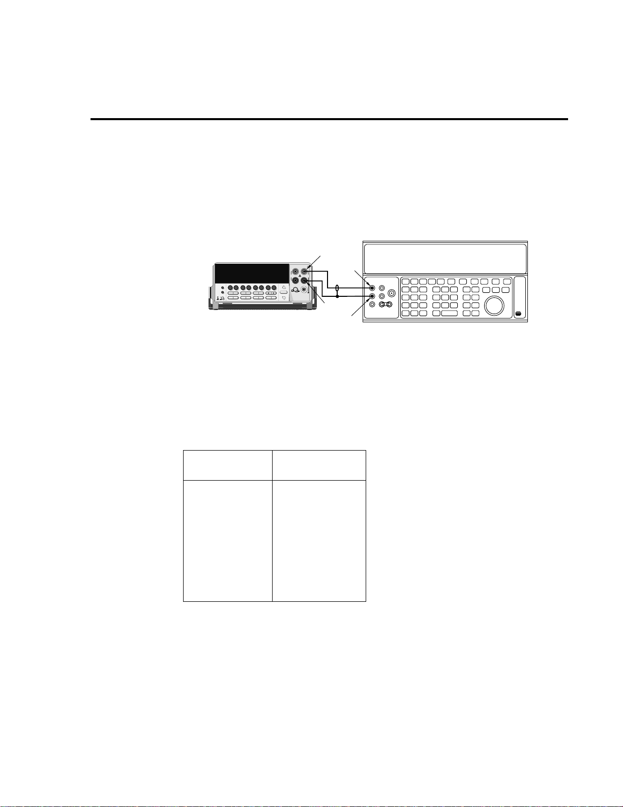
Figure 1-1
Connections for
DC volts verification
5700A Calibrator (Output DC Voltage)
Model 2010
2000 MULTIMETER
Input HI
Output HI
!
R
Input
LO
Output
LO
Note : Use shielded, low-thermal cables
for 100mV and 1V ranges.
2. Select the DC volts function by pressing the DCV key, and set the Model 2010 to the
100mV range.
3. Set the calibrator output to 0.00000mV DC, and allow the reading to settle.
4. Enable the Model 2010 REL mode. Leave REL enabled for the remainder of the DC
volts verification tests.
5. Source positive and negative full-scale voltages for each of the ranges listed in Table 1-
2. For each voltage setting, be sure that the reading is within stated limits.
Table 1-2
DCV reading limits
Range
100mV
1V
10V
100V
1000V
* Source positive and negative values for each range.
Applied DC
voltage*
100.0000mV
1.000000V
10.00000V
100.0000V
1000.000V
Reading limits
(1 year, 18°C–28°C)
99.99540 to 100.00460mV
0.9999730 to 1.0000270V
9.999720 to 10.000280V
99.99600 to 100.00400V
999.9530 to 1000.0470V
Page 19
1-8 Performance Verification
V erifying AC voltage
Check AC voltage accuracy by applying accurate AC voltages at specific frequencies from
the A C v oltage calibrator to the Model 2010 inputs and verifying that the displayed readings f all
within specified ranges.
Figure 1-2
Connections for
AC volts verification
CAUTION Do not exceed 1000V peak between INPUT HI and INPUT LO, or 8
V•Hz input, because instrument damage may occur.
Follow these steps to verify AC voltage accuracy:
1. Connect the Model 2010 HI and LO INPUT jacks to the A C voltage calibrator as sho wn
in Figure 1-2.
5725 Amplifier (Connect to calibrator)
Note: 5725 Amplifier required only
for 700V, 50kHz output.
Model 2010
2000 MULTIMETER
Input HI
Output HI
!
R
Input
LO
Shielded cable
Output
LO
5700A Calibrator (Output AC Voltage)
2. Select the AC volts function by pressing the ACV key.
3. Set the Model 2010 for the 100mV range; make sure that REL is disabled.
4. Source 1kHz and 50kHz AC voltages for each of the ranges summarized in Table 1-3,
and make sure that the respective Model 2010 readings fall within stated limits.
7
×
10
Page 20

Table 1-3
ACV reading limits
Performance Verification 1-9
ACV
range
Applied
AC voltage
(1 year, 18°C–28°C)
1kHz 50kHz
Reading limits
100mV
1V
10V
100V
750V
*If the 5725A amplifier is not available, change the 700V at 50kHz step to 220V at 50kHz.
(Reading limits for 220V at 50kHz = 219.361 to 220.639V).
100.0000mV
1.000000V
10.00000V
100.0000V
700.000V*
99.910 to 100.090mV
0.99910 to 1.00090V
9.9910 to 10.0090V
99.910 to 100.090V
699.36 to 700.64V
99.830 to 100.170mV
0.99830 to 1.00170V
9.98300 to 10.0170V
99.830 to 100.170V
698.79 to 701.21V
Page 21
1-10 Performance Verification
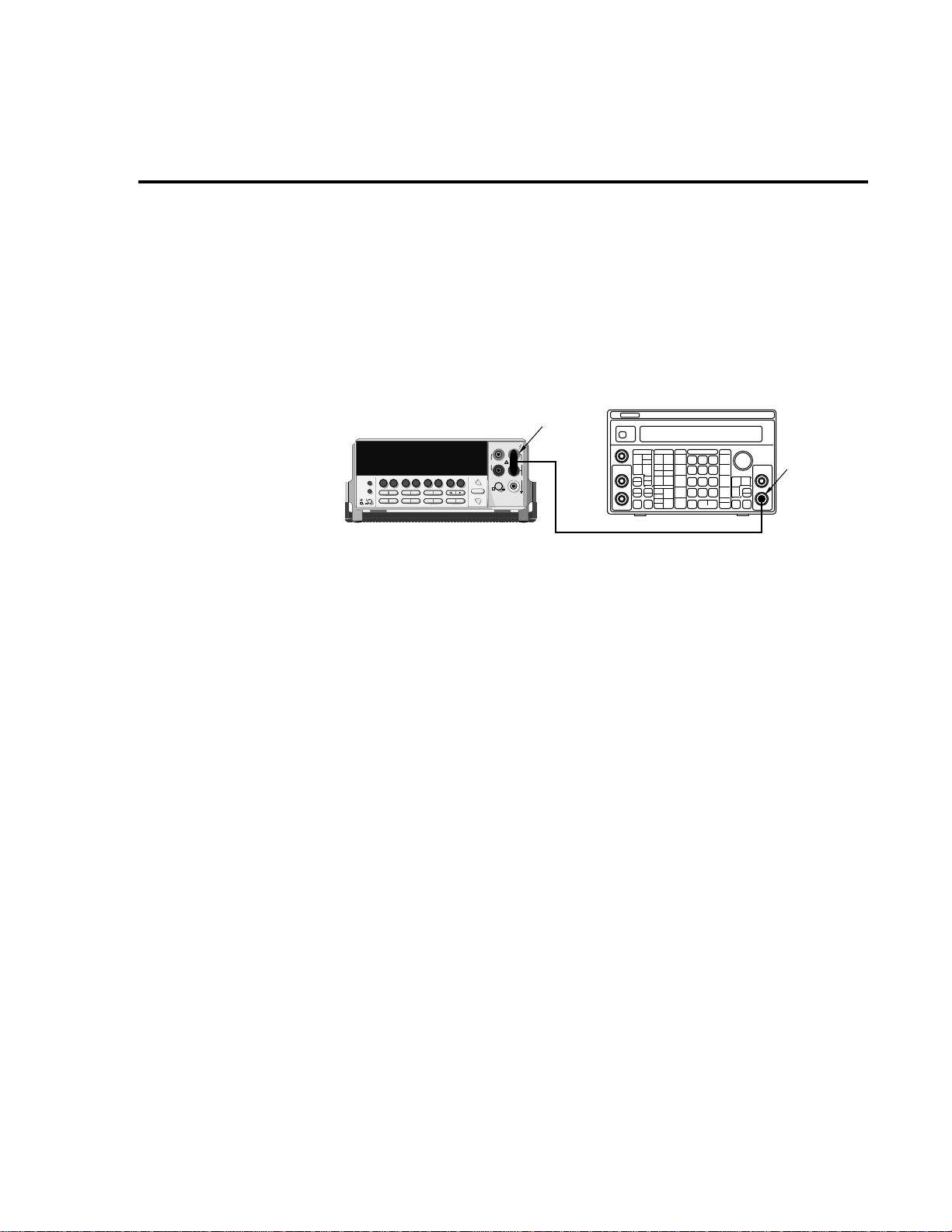
V erifying DC current
Check DC current accuracy by applying accurate DC currents from the DC current calibrator
to the AMPS input of the Model 2010 and v erifying that the displayed readings f all within specified limits. Follow these steps to verify DC current accuracy:
1. Connect the Model 2010 AMPS and INPUT LO jacks to the calibrator as shown in Figure 1-3.
2. Select the DC current measurement function by pressing the DCI key.
3. Set the Model 2010 for the 10mA range.
4. Source positive and negati v e full-scale currents for each of the ranges listed in Table 1-4,
and verify that the readings for each range are within stated limits.
Figure 1-3
Connections for
DC current verification
5700A Calibrator (Output DC Current)
Model 2010
2000 MULTIMETER
Input
LO
Output HI
!
R
Amps
Output
LO
Note: Be sure calibrator is set for
normal current output.
Table 1-4
DCI limits
DCI
range
10mA
100mA
1A
3A
*Source positive and negative currents with values shown.
Applied DC
current*
10.0000mA
100.0000mA
1.000000A
2.20000A
Reading limits
(1 year, 18°C–28°C)
9.994600 to 10.005400mA
99.94600 to 100.05400mA
0.9991600 to 1.0008400A
2.197315 to 2.202685A
Page 22
V erifying AC current
Check A C current accurac y by applying accurate AC current at specific frequencies from the
AC current calibrator to the Model 2010 input and verifying that the displayed readings fall
within specified limits. Follow these steps to verify AC current:
1. Connect the Model 2010 AMPS and INPUT LO jacks to the calibrator as shown in Figure 1-4.
2. Select the AC current function by pressing the ACI key.
3. Set the Model 2010 for the 1A range.
4. Source 1A and 2.2A, 1kHz full-scale AC currents as summarized in T able 1-5, and verify
that the readings are within stated limits.
Performance Verification 1-11
Figure 1-4
Connections for
AC current verification
Model 2010
Table 1-5
ACI limits
ACI
range
1A
3A
!
2000 MULTIMETER
R
Amps
Applied DC
voltage
1.000000A
2.20000A
Output HI
Input
LO
Output
LO
5700A Calibrator (Output AC Current)
Reading limits
(1 year, 18°C–28°C) 1kHz
0.99860 to 1.00140A
2.1949 to 2.2051A
Page 23

1-12 Performance Verification
V erifying resistance
Check resistance by connecting accurate resistance values to the Model 2010 and verifying
that its resistance readings are within the specified limits.
CAUTION Do not apply more 1000V peak between INPUT HI and LO or more than
350V peak between SENSE HI and LO, or instrument damage could occur.
Follow these steps to verify resistance accuracy:
1. Using shielded 4-wire connections, connect the Model 2010 INPUT and SENSE jacks
to the calibrator as shown in Figure 1-5.
Figure 1-5
Connections for
resistance verifi-
Ω
cation (10
-
10MΩ ranges)
5700A Calibrator
Sense LO
Model 2010
2000 MULTIMETER
Sense LO
Sense HI
!
R
Sense HI
Input
HI
Output
HI
InputLOOutput
LO
Note : Use shielded low-thermal cables to
minimize noise. Enable or disable
calibrator external sense as indicated
in procedure.
2. Set the calibrator for 4-wire resistance with external sense on.
3. Select the Model 2010 4-wire resistance function by pressing the
4. Set the Model 2010 for the 10
calibrator output to 0
Ω , then enable Model 2010 REL.
Ω range, and make sure the FILTER is on. Set the
Ω 4 key.
5. Recalculate reading limits based on actual calibrator resistance values.
6. Source the nominal full-scale resistance values for the 10
Ω -10M Ω ranges summarized
in Table 1-6, and verify that the readings are within calculated limits.
7. Connect the Model 2010 INPUT and SENSE jacks to the calibrator as shown in Figure
1-6.
8. Disable external sense on the calibrator.
9. Set the Model 2010 for the 100M
10. Source a nominal 100M
lated limits for the 100M
Ω resistance value, and verify that the reading is within calcu-
Ω range.
Ω range.
Page 24
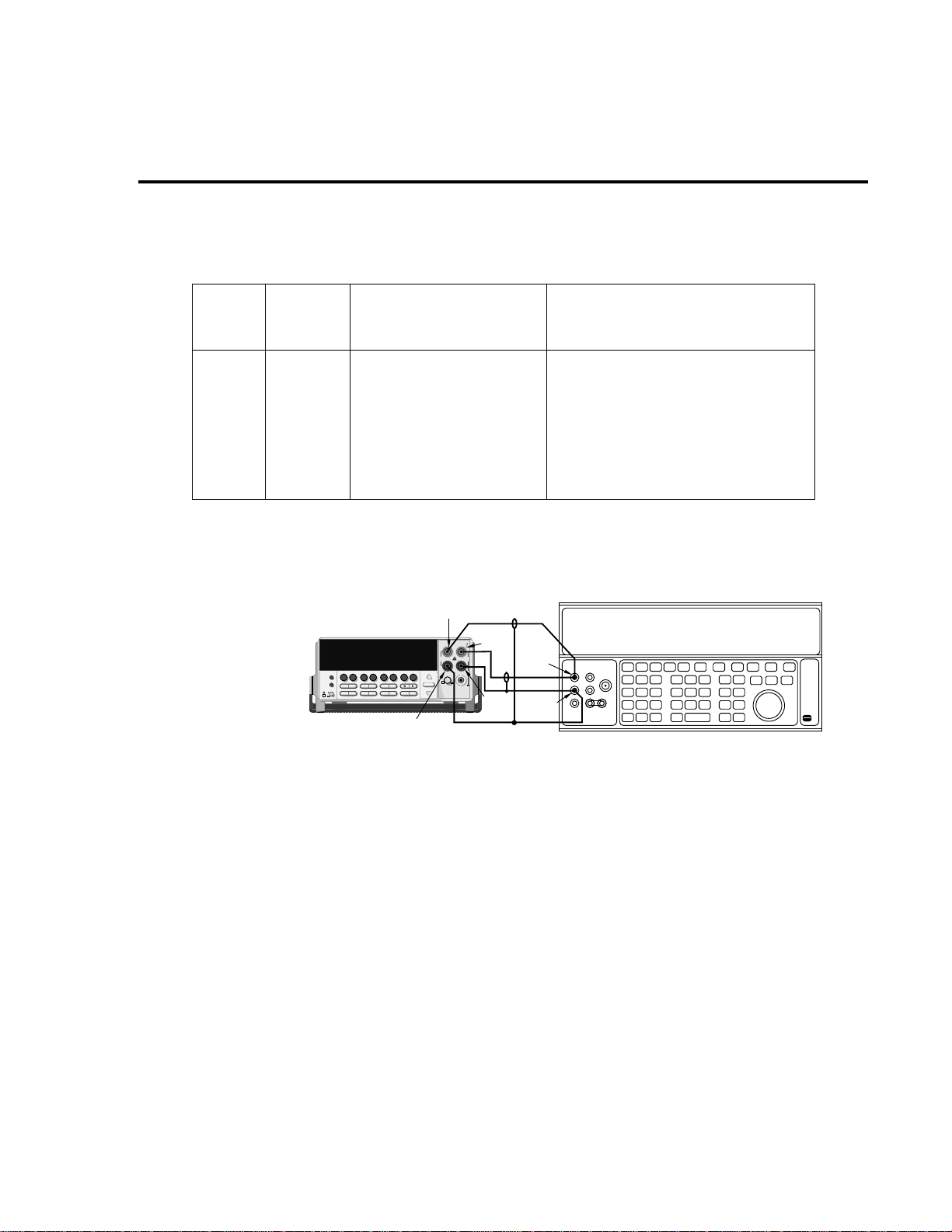
Table 1-6
Limits for resistance verification
Nominal
Ω range
applied
resistance
Nominal reading limits
Performance Verification 1-13
(1 year, 18°C–28°C) Recalculated limits*
10 Ω
100 Ω
1k Ω
10k Ω
100k Ω
1M Ω
10M Ω
100M Ω
* See verification limits.
Figure 1-6
Connections for
resistance verifi-
Ω
cation (100M
range)
10 Ω
100 Ω
1k Ω
10k Ω
100k Ω
1MΩ
10MΩ
100MΩ
9.999310 to 10.000690Ω
99.99390 to 100.00610Ω
0.9999480 to 1.0000520kΩ
9.999480 to 10.000520kΩ
99.99080 to 100.00920kΩ
0.9999260 to 1.0000740MΩ
9.995960 to 10.004040MΩ
99.84960 to 100.15040MΩ
Sense HI
Model 2010
2000 MULTIMETER
Sense LO
!
R
Input
HI
InputLOOutput
______________to_____________ Ω
______________to_____________ Ω
______________to_____________ kΩ
______________to_____________ kΩ
______________to_____________ kΩ
______________to_____________ MΩ
______________to_____________ MΩ
______________to_____________ MΩ
5700A Calibrator (Output 2-wire Resistance)
Output
HI
LO
Note : Use shielded cables to minimize noise.
Disable calibrator external sense mode.
Page 25

1-14 Performance Verification
V erifying temperature
Thermocouple and RTD temperature readings are derived from DC volts and ohms readings
respectively. For this reason, it is not necessary to independently verify the accuracy of temperature measurements. As long as the DC v olts and ohms functions meet or exceed their respecti ve
specifications, temperature function accuracy is automatically verified. However, temperature
verification procedures are provided belo w for those who wish to separately v erify temperature
accuracy.
Thermocouple temperature
1. Connect the DC voltage calibrator output terminals to the Model 2010 INPUT jacks using low-thermal shielded connections. (Use 2-wire connections similar to those shown
in Figure 1-1.)
2. Configure the Model 2010 for °C units, type J temperature sensor, and 0°C simulated reference junction as follows:
A. Press SHIFT then SENSOR, and note the unit displays the temperature units:
UNITS: C. (If necessary, use the cursor and range keys to select °C units.)
B. Press ENTER, and note the unit displays the sensor type: SENS: TCOUPLE. (Use
the cursor and range keys to select a thermocouple type temperature sensor.)
C. Press ENTER. The unit then displays the thermocouple type: TYPE: J.
D. Select a type J temperature sensor, and then press ENTER. The unit displays the ref-
erence junction type: JUNC: SIM.
E. Make sure the simulated reference junction type is selected, and then press ENTER.
The unit displays the current simulated reference junction temperature: SIM: 023.
F . Using the cursor and range keys, set the reference junction temperature to 0°C, and
then press ENTER to complete the temperature configuration process.
Page 26

Performance Verification 1-15
3. Select the temperature function by pressing the TEMP key.
4. Source each of the voltages summarized in Table 1-7, and verify that the temperature
readings are within limits. Be sure to select the appropriate thermocouple type for each
group of readings. (See step 2.)
Table 1-7
Thermocouple temperature verification reading limits
Thermocouple
type
J
K
* Voltages shown are based on ITS-90 standard using 0°C reference
junction temperature. See text for procedure to set reference junction
temperature.
Applied DC
voltage*
-7.659mV
0mV
42.281mV
-5.730mV
0mV
54.138mV
Reading limits
(1 year, 18°C–28°C)
-190.60 to -189.40°C
-0.50 to +0.50°C
749.50 to 750.50°C
-190.60 to -189.40°C
-0.50 to +0.50°C
1349.20 to 1350.80°C
Page 27

1-16 Performance Verification
RTD temperature
1. Connect the precision decade resistance box (listed in Table 1-1) to the Model 2010
INPUT and SENSE jacks using 4-wire connections. (See Figure 1-1 for a similar
connecting scheme.)
2. Configure the Model 2010 temperature function for °C units and RTD temperature sensor (α=0.00385) as follows:
A. Press SHIFT then SENSOR, and note the unit displays the temperature units:
UNITS: C.
B. Press ENTER, and note the unit displays the sensor type: SENS: TCOUPLE.
C. Using the cursor and range keys, set the display as follows: SENS: 4W-RTD.
D. Press ENTER, and note the unit displays: TYPE: PT100.
E. Using the cursor and range keys, set the unit for the following display: TYPE:
PT385.
F. Press ENTER to complete the temperature configuration process.
3. Select the temperature function by pressing the TEMP key.
4. Set the decade resistance box to each of the values shown in Table 1-8, and verify that
the temperature readings are within the required limits.
Table 1-8
Four-wire RTD temperature verification reading limits
Applied
resistance*
22.80Ω
100.00Ω
313.59Ω
* Based on a = 0.00385. See text.
Reading limits (°C)
(1 year, 18°C–28°C)
-190.14 to -189.86°C
-0.08 to +0.08°C
599.86 to 600.14°C
Page 28
V erifying frequency
Follow the steps below to verify the Model 2010 frequency function.
1. Connect the frequency synthesizer to the Model 2010 INPUT jacks. See Figure 1-7.
2. Set the synthesizer to output a 1kHz, 1V RMS sine wave.
3. Select the Model 2010 frequency function by pressing the FREQ key.
4. Verify that the Model 2010 frequency reading is between 999.9000Hz and 1.000100kHz.
Performance Verification 1-17
Figure 1-7
Connections for
frequency verification
Model 2010
2000 MULTIMETER
!
R
BNC-to-Dual
Banana Plug
Adapter
50Ω BNC Coaxial Cable
Model 3930A or 3940 Synthesizer
Main
Function
Output
Page 29
1-18 Performance Verification
V erifying ratio
CAUTION When verifying ratio or using sense volts, the SENSE LO terminal must be
1. Connect SENSE HI to INPUT HI, and connect SENSE LO to INPUT LO.
2. Connect the DC calibrator output HI and LO terminals to the Model 2010 HI and LO
terminals respectively, as shown in Figure 1-8.
3. Select the Model 2010 DCV function, and select the 1V range.
4. Set the DC calibrator output to +1.000000V DC, and turn on its output.
5. Press SHIFT then RATIO, then select and enable both RATIO:ON and SENSEIN:ON.
6. Verify that the ratio reading is between 0.9999460 and 1.0000540.
referenced to INPUT LO. Exceeding 350V DC from SENSE HI to SENSE
LO will cause instrument damage.
Figure 1-8
Verifying ratio
STEP CH2 CH3 CH4 CH5 CH6 CH7 CH8 CH9 CH10
TALK
LSTN
SRQ
SHIFT
TIMER
HOLD TRIG FAST MED SLOW AUTO ERR
MX+B
SHIFT
DCV
LOCAL
EX TRIG
POWER
SAVE SETUP
OPEN CLOSE
Model 2010
CH1REM
SCAN
REL FILT
dBm
%
dB
ACI
ACV
DCI
HOLD
LIMITS ON/OFFDELAY
TRIG
STORE
RECALL
CONFIG HALT
STEP SCAN
CONT
DIGITS RATE
Ω2 Ω4
TYPE
GPIB
BUFFER
RATIO
RELFILTER
RS232
SENSE HI
MATH
REAR
4W
STAT
2010 MULTIMETER
PERIOD SENSOR
FREQ
TEMP
DRYCKT O COMP
CAL TEST
EXIT ENTER
Model 5700A
HI
SENSE
INPUT
Ω 4 WIRE
HI
350V
1000V
!
PEAK
PEAK
LO
500V
PEAK
INPUTS
F
R
RANGE
AUTO
FRONT/REAR
3A 250V
AMPS
RANGE
Short SENSE HI to INPUT HI
Short SENSE LO to INPUT LO
LOSENSE LO
Page 30

2
Calibration
Page 31

2-2 Calibration
Introduction
Use the procedures in this section to calibrate the Model 2010. Calibration procedures in-
clude:
• Comprehensive calibration: calibrate DC and AC voltages, DC and AC currents, and resistance values.
• Manufacturing calibration: usually only performed at the factory
WARNING The information in this section is intended for qualified service personnel
only. Do not attempt these procedures unless you are qualified to do so.
All the procedures require accurate calibration equipment to supply precise DC and AC voltages, DC and A C currents, and resistance v alues. Comprehensi v e A C and DC calibration can be
performed any time by an operator either from the front panel, or by using the SCPI commands
sent either over the IEEE-488 bus or the RS-232 port. DC-only and AC-only calibration may be
performed individually, if desired.
NOTE Manufacturing calibration is normally requir ed in the field only if the Model 2010 has
been repaired.
Page 32

Calibration 2-3
Environmental conditions
Conduct the calibration procedures in a location that has:
• An ambient temperature of 18-28°C (65-82°F)
• A relative humidity of less than 80% unless otherwise noted
W arm-up period
Allow the Model 2010 Multimeter to warm up for at least tw o hours before performing cali-
bration.
If the instrument has been subjected to temperature extremes (those outside the ranges stated
in the above section), allow e xtra time for the instrument’ s internal temperature to stabilize. Typically, allow one extra hour to stabilize a unit that is 10°C (18°F) outside the specified temperature range.
Also, allow the test equipment to warm up for the minimum time specified by the manufacturer.
Line power
The Model 2010 Multimeter requires a line voltage of 100V/120V/220V/240V, ±10% and a
line frequency of 45Hz to 66Hz, or 360Hz to 440Hz.
Page 33

2-4 Calibration
Calibration considerations
When performing the calibration procedures:
• Make sure that the equipment is properly warmed up and connected to the appropriate
input jacks. Also make sure that the correct input jacks are selected with the INPUTS
switch.
• Make sure the calibrator is in operate before you complete each calibration step.
• Always let the source signal settle before calibrating each point.
• Do not connect test equipment to the Model 2010 through a scanner or other switching
equipment.
• If an error occurs during calibration, the Model 2010 will generate an appropriate error
message. See Appendix B for more information.
• Always allow the calibrator to settle before pressing ENTER to complete each step.
(There is a “u” on the display of the 5700A Calibrator that is the settle annunciator).
W ARNING The maximum common-mode voltage (voltage between INPUT LO and chas-
sis ground) is 500V peak. Exceeding this value may cause a breakdown in insulation, creating a shock hazard. Some of the procedures in this section may
expose you to dangerous voltages. Use standard safety precautions when
such dangerous voltages are encountered to avoid personal injury caused by
electric shock.
Page 34

Calibration code
Before performing comprehensive calibration, you must first unlock calibration by entering
the appropriate calibration code.
Front panel code
For front panel calibration, follow these steps:
1. Access the calibration menu by pressing SHIFT CAL, and note that the instrument dis-
Calibration 2-5
plays the following:
CAL: DATES
2. Use the up or down range key to scroll through the a v ailable calibration parameters until
the unit displays RUN, and then press ENTER.
3. The Model 2010 then prompts you to enter a code:
CODE? 000000
The factory default code is 002010. Use the left and right arro w keys to mo ve among the
digits, use the up range key to increment numbers, and press the do wn range key to specify alphabetic letters. Confirm the code by pressing ENTER.
4. The Model 2010 lets you define a new calibration code. Use the up and do wn range keys
to toggle between yes and no. Choose N if you do not want to change the code. Choose
Y if you want to change the code. The unit then prompts you to enter a ne w code. Enter
the code, and press ENTER.
Remote command code
If you are performing calibration over the IEEE-488 b us or the RS-232 port, send the follo w-
ing command to unlock calibration:
CAL:PROT:CODE '<8-character string>'.
The default code command is:
CAL:PROT:CODE 'KI002010'.
NOTE If the first two characters ar e anything other than “KI”, you will not be able to unloc k
cal from the front panel.
Page 35

2-6 Calibration
Comprehensive calibration
The comprehensive calibration procedure calibrates the DCV, DCI, ACV, ACI, and ohms
functions. You can also choose to calibrate only the DCV/DCI and resistance, or the ACV/ACI
functions.
These procedures are usually the only ones required in the field. Manufacturing calibration is
done at the factory and can be done in the field if the unit has been repaired. See Manufacturing
calibration at the end of this section for more information.
Calibration cycle
Perform comprehensive calibration at least e v ery other year, once a year, or e v ery 90 days to
ensure the unit meets the corresponding specifications.
Recommended equipment
Table 2-1 lists the recommended equipment you need for comprehensive, DC only, and AC
only calibration procedures. You can use alternate equipment, such as a DC transfer standard and
characterized resistors, as long as that equipment has specifications at least as good as those listed in the table.
Table 2-1
Recommended equipment for comprehensive, DC-only, or AC-only calibration
Fluke 5700A calibrator:
DC voltage
±10V:±5ppm
100V:±7ppm
AC voltage
(1kHz, 50kHz)*
10mV:±710ppm
100mV:±200ppm
1.0V:±82ppm
10V:±82ppm
100V:±90ppm
700V:±85ppm
DC current
10mA:±60ppm
100mA:±70ppm
1A:±110ppm
AC current
(1kHz)
100mA:±190ppm
1A:±690ppm
2A:±670ppm
Resistance
10
Ω :±28ppm
1k
Ω :±12ppm
10k
Ω :±11ppm
100k
Ω :±13ppm
1M
Ω :±18ppm
Keithley 8610 Low-thermal shorting plug
* 1kHz specifications. 10mV and 700V points require 1kHz only. All calibrator specifications are 90-
day, 23°C ±5°C specifications and indicate total absolute uncertainty at specified output.
Page 36

Aborting calibration
You can abort the front panel calibration process at any time by pressing EXIT. The instru-
ment will then ask you to confirm your decision to abort with the following message:
ABORT CAL?
Press EXIT to abort calibration at this point, or press any other key to return to the calibration
process.
NOTE The Model 2010 will not respond to any remote programming commands while the
ABORT CAL? message is displayed.
Calibration 2-7
Page 37

2-8 Calibration
Front panel calibration
Use the following steps for comprehensive, DC-only, and AC-only calibration procedures.
The procedures for front panel calibration include:
• Preparing the Model 2010 for calibration
• Front panel short and open calibration
• DC voltage calibration
• Resistance calibration
• DC current calibration
• AC voltage calibration
• AC current calibration
• Setting calibration dates
Preparing the Model 2010 for calibration
1. Turn on the Model 2010, and allo w it to warm up for at least two hours before performing
calibration procedure.
2. Start the calibration process as follows:
A. Access the calibration menu by pressing SHIFT then CAL.
B. Use the up and down range keys to scroll through the available calibration menu
items until the unit displays RUN, and then press ENTER.
C. At the prompt, enter the calibration code. (The default code is 002010.) Use the left
and right arrow keys to move among the digits, use the up range key to increment
numbers, and press the down range key to specify alphabetic letters. Confirm the
code by pressing ENTER.
D. Choose N at the prompt to proceed without changing the code, and then press EN-
TER.
3. Choose which of the calibration tests summarized in Table 2-2 you want to run at the
CAL: RUN prompt. Use the up and do wn range keys to scroll through the options; select
your choice by pressing ENTER.
Table 2-2
Comprehensive calibration procedures
Procedure
Full calibration
DCV, DCI, and ohms
ACV and ACI
Menu
choice Procedures
ALL
DC
AC
All comprehensive calibration steps.
DC voltage, DC current, and resistance calibration.
AC voltage and AC current.
Page 38

Front panel short and open calibration
At the Model 2010 prompt for a front panel short, perform the following:
1. Connect the Model 8610 low-thermal short to the instrument front panel INPUT and
SENSE terminals as shown in Figure 2-1. Make sure the INPUTS button is not pressed
in so that the front inputs are selected. Wait at least three minutes before proceeding to
allow for thermal equilibrium.
NOTE Be sure to connect the low-thermal short properly to the HI, LO, and SENSE termi-
nals. Keep drafts away from low-thermal connections to avoid thermal drift, which
could affect calibration accuracy.
Calibration 2-9
Figure 2-1
Low-thermal
short connections
Model 2010
S+ HI
2000 MULTIMETER
!
R
Model 8610
low-thermal
short
LOS-
2. Press ENTER to start short-circuit calibration. While the unit is calibrating, the unit will
display:
CALIBRATING
3. When the unit is done calibrating, it will display the following prompt:
OPEN CIRCUIT
4. Remove the calibration short, and press ENTER. During this phase, the CALIBRATING
message will be displayed.
Page 39

2-10 Calibration
DC volts calibration
After the front panel short and open procedure, the unit will prompt you for the first DC volt-
age: +10V. Perform the following:
1. Connect the calibrator to the Model 2010 as shown in Figure 2-2. Wait three minutes to
allow for thermal equilibrium before proceeding.
NOTE Although 4-wire connections are shown, the sense leads are connected and discon-
nected at various points in this procedure by turning calibrator external sense on or
off as appropriate. If your calibrator does not have provisions for turning external
sense on and off, disconnect the sense leads when external sensing is to be turned of f ,
and connect the sense leads when external sensing is to be turned on. Do not exceed
±15V peak on sense LO to LO. This will cause erroneous r eadings to be stored during
calibration.
Figure 2-2
Calibrator connections for DC
volts and ohms
portion of comprehensive calibration
5700A Calibrator
Sense LO
Model 2010
2000
Sense LO
Sense HI
MULTIMETER
!
R
Sense HI
Input
HI
Output
HI
InputLOOutput
LO
Note : Use shielded low-thermal cables to
minimize noise. Enable or disable
calibrator external sense as indicated
in procedure.
2. Set the calibrator to output DC volts, and turn external sense off.
3. Perform the steps listed in Table 2-3 to complete DC volts calibration. For each calibration step:
• Set the calibrator to the indicated value, and make sure it is in operate.
• Press the ENTER key to calibrate that step.
• Wait until the Model 2010 finishes each step. The unit will display the CALIBRATING message while calibrating.
Page 40

NOTE If your calibrator cannot output the values recommended in T able 2-3, use the left and
right arrow ke ys, and the up and down rang e keys to set the Model 2010 display value
to match the calibrator output voltage.
Table 2-3
DC volts calibration summary
Calibration 2-11
Calibration
step
+10V
-10V
100V
Calibrator
voltage
+10.00000V
-10.00000V
+100.0000V
Resistance calibration
Completing the 100V DC calibration step ends the DC voltage calibration procedure. The
Model 2010 will then prompt you to connect 10
1. Set the calibrator output for resistance, and turn on external sense.
NOTE Use external sense (4-wire
calibrator external sense mode is turned on.
2. Perform the calibration steps summarized in Table 2-4. For each step:
• Set the calibrator to the indicated value, and place the unit in operate. (If the calibrator
cannot output the exact resistance value, use the Model 2010 left and right arro w ke ys
and the range keys to adjust the Model 2010 display to agree with the calibrator resistance.)
• Press the ENTER key to calibrate each point.
• Wait for the Model 2010 to complete each step before continuing.
Allowable
range
+9V to +11V
-9V to -11V
+90V to +110V
Ω . Follow these steps for resistance calibration:
Ω
) when calibrating all resistance r anges. Be sur e that the
Table 2-4
Ohms calibration summary
Calibration
step
10 Ω
1k Ω
10k Ω
100k Ω
1M Ω
* Nominal resistance. Adjust Model 2010 calibration
parameter to agree with actual value.
Calibrator
resistance*
10 Ω
1k Ω
10k Ω
100k Ω
1M Ω
Allowable range
9 Ω to 11 Ω
0.9k Ω to 1.1k Ω
9k Ω to 11k Ω
90k Ω to 110k Ω
0.9M Ω to 1.1M Ω
Page 41

2-12 Calibration
DC current calibration
After the 1M Ω resistance point has been calibrated, the unit will prompt you for 10mA. Fol-
low these steps for DC current calibration:
1. Connect the calibrator to the AMPS and INPUT LO terminals of the Model 2010 as
shown in Figure 2-3.
Figure 2-3
Connections for
DC and AC amps
comprehensive
calibration
5700A Calibrator
Model 2010
2000
MULTIMETER
Input
LO
Output HI
!
R
Amps
Output
LO
Note: Be sure calibrator is set for
normal current output.
2. Calibrate each current step summarized in Table 2-5. For each step:
• Set the calibrator to the indicated DC current, and make sure the unit is in operate.
• Make sure the Model 2010 display indicates the correct calibration current.
• Press ENTER to complete each step.
• Allow the Model 2010 to finish each step.
NOTE If you are performing DC-only calibration, proceed to Setting calibration dates.
Table 2-5
DC current calibration summary
Calibration
step
Calibrator
current
Allowable
range
10mA
100mA
1A
10.00000mA
100.0000mA
1.000000A
9mA to 11mA
90mA to 110mA
0.9A to 1.1A
Page 42
AC voltage calibration
Follow these steps for AC voltage calibration:
1. Connect the calibrator to the Model 2010 INPUT HI and LO terminals as shown in Figure 2-4.
Calibration 2-13
Figure 2-4
Connections for
AC volts calibration
5700A Calibrator
R
!
Input HI
Output HI
Input
LO
Output
LO
Model 2010
2000 MULTIMETER
2. Perform the calibration steps summarized in Table 2-6. For each step:
• Set the calibrator to the indicated value, and make sure the calibrator is in operate.
• Press ENTER to complete each step.
• Wait until the Model 2010 completes each step.
Table 2-6
AC voltage calibration summary
Calibration step
10mV AC at 1kHz
100mV AC at 1kHz
100mV AC at 50kHz
1V AC at 1kHz
1V AC at 50kHz
10V AC at 1kHz
10V AC at 50kHz
100V AC at 1kHz
100V AC at 50kHz
700V AC at 1kHz
Calibrator voltage,
frequency
10.00000mV, 1kHz
100.0000mV, 1kHz
100.0000mV, 50kHz
1.000000V, 1kHz
1.000000V, 50kHz
10.00000V, 1kHz
10.00000V, 50kHz
100.0000V, 1kHz
100.0000V, 50kHz
700.000V, 1kHz
NOTE Do not exceed ±15V peak between sense LO and LO. You may have to remove the ex-
ternal sense leads before calibrating AC volts. Even though some calibr ators can turn
off their external sense, the AC voltage can still cause excess voltage to appear between sense LO and LO.
Page 43

2-14 Calibration
AC current calibration
After the 700V AC at 1kHz point has been calibrated, the unit will prompt you for 100mA at
1kHz. Follow these steps for AC current calibration:
1. Connect the calibrator to the AMPS and INPUT LO terminals of the Model 2010 as
shown in Figure 2-3.
2. Perform the calibration steps summarized in Table 2-7. For each step:
• Set the calibrator to the indicated current and frequency, and make sure the unit is in
operate.
• Press ENTER to complete each calibration step.
• Allow the unit to complete each step before continuing.
Table 2-7
AC current calibration summary
Calibration
step
100mA at 1kHz
1A at 1kHz
2A at 1kHz
Calibrator current,
frequency
100.0000mA, 1kHz
1.000000A, 1kHz
2.000000A, 1kHz
Page 44

Setting calibration dates
At the end of the calibration procedure, the instrument will display the CALIBRATION
COMPLETE message. Press ENTER to continue, and the Model 2010 will prompt you to enter
the calibration date and the calibration due date. Set these dates as follows:
1. At the CAL DATE: mm/dd/yy prompt, use the left and right arrow keys and the range
keys to set the calibration date, and then press ENTER.
2. The unit will then prompt you to enter the next calibration due date with this prompt:
CAL NDUE: mm/dd/yy. Use the left and right arrow keys and the range keys to set the
calibration due date, and then press ENTER.
3. The unit will prompt you to save new calibration constants with this message: SAVE
CAL? YES. To save the new constants, press ENTER. If you do not want to sa ve the ne w
constants, press the down range key to toggle to NO, and then press ENTER.
Calibration 2-15
NOTE Calibration constants calculated during the curr ent calibration pr ocedur e will not be
saved unless you choose the YES option. Previous calibration constants will be retained if you select NO.
If an incorrect date is enter ed, the “INVALID DATE” message will be displayed. The
menu will remain until a valid date is entered.
Page 45

2-16 Calibration
Remote calibration
Use the following steps to perform comprehensi ve, DC-only, and AC-only calibration procedures by remote. See Appendix B for a detailed list and description of SCPI calibration commands.
When sending calibration commands, be sure that the Model 2010 completes each step before
sending the next command. You can do so by observing the front panel CALIBRATING message or by detecting the completion of each step over the bus.
The procedures for calibrating the Model 2010 using SCPI commands include:
• Preparing the Model 2010 for calibration
• Front panel short and open calibration
• DC volts calibration
• Resistance calibration
• DC current calibration
• AC volts calibration
• AC current calibration
• Programming calibration dates
• Saving calibration constants
• Locking out calibration
NOTE As with front panel calibr ation, you can c hoose to perform comprehensive, DC-only ,
or AC-only calibr ation. Be sur e to include a space char acter between each command
and parameter.
Page 46

Preparing the Model 2010 for calibration
1. Connect the Model 2010 to the IEEE-488 bus of the computer using a shielded IEEE488 cable, such as the Keithley Model 7007, or connect the unit to a computer through
the RS-232 port using a straight-through 9-pin to 9-pin cable (use a 9-25-pin adapter if
necessary).
2. Turn on the Model 2010, and allow it to warm up for two hours before performing calibration.
3. Select the DCV function, and choose SLOW as the rate (integration time = 5PLC).
4. Make sure the primary address of the Model 2010 is the same as the address specified in
the program that you will be using to send commands. Use the GPIB key.
5. Unlock the calibration function by sending this command:
:CAL:PROT:CODE 'KI002010'
Calibration 2-17
(The above command shows the default code, KI002010. Substitute the correct code if
changed.)
6. Send the following command to initiate calibration:
:CAL:PROT:INIT
Short and open calibration
1. Connect the Model 8610 low-thermal short to the instrument INPUT and SENSE terminals as shown in Figure 2-1. Make sure the INPUTS b utton is not pressed in so that the
front inputs are active. W ait at least three minutes before proceeding to allo w for thermal
equilibrium.
NOTE Be sure to connect the low-thermal short properly to the HI, LO, and SENSE termi-
nals. Keep drafts away from low-thermal connections to avoid thermal drift, which
could affect calibration accuracy.
2. Send the following command:
:CAL:PROT:DC:STEP1
3. After the Model 2010 completes this step, remove the low-thermal short and send this
command:
:CAL:PROT:DC:STEP2
Page 47

2-18 Calibration
DC volts calibration
After front panel short and open steps, perform the following:
1. Connect the calibrator to the Model 2010 as shown in Figure 2-2. Allow three minutes
for thermal equilibrium.
NOTE Although 4-wire connections are shown, the sense leads are connected and discon-
nected at various points in this procedure by turning calibrator external sense on or
off as appropriate. If your calibrator does not have provisions for turning external
sense on and off, disconnect the sense leads when external sensing is to be turned of f ,
and connect the sense leads when external sensing is to be turned on. Disconnect
sense leads when calibrating and verifying AC volts.
NOTE Disconnect sense leads when calibrating and verifying AC volts.
2. Perform the calibration steps summarized in Table 2-8. For each step:
• Set the calibrator to the indicated voltage, and make sure the unit is in operate. (Use
the recommended voltage if possible.)
• Send the indicated programming command. (Change the voltage parameter if you are
using a different calibration voltage.)
• Wait until the Model 2010 completes each step before continuing.
Table 2-8
DC voltage calibration programming steps
Calibration
step
+10V
-10V
100V
* Change parameter accordingly if using a different calibrator voltage.
Calibrator
voltage
+10.00000V
-10.00000V
100.0000V
Calibration command*
:CAL:PROT:DC:STEP3 10
:CAL:PROT:DC:STEP4 -10
:CAL:PROT:DC:STEP5 100
Parameter
range
9 to 11
-9 to -11
90 to 110
Page 48

Resistance calibration
Follow these steps for resistance calibration:
1. Set the calibrator to the resistance mode, and turn on external sensing.
Calibration 2-19
NOTE Use external sense (4-wire
calibrator external sense mode is turned on,
2. Perform the calibration steps summarized in Table 2-9. For each step:
• Set the calibrator to the indicated resistance, and make sure the unit is in operate.
(Use the recommended resistance or the closest available value.)
• Send the indicated programming command. (Change the command parameter if you
are using a different calibration resistance than that shown.)
• Wait until the Model 2010 completes each step before continuing.
Table 2-9
Resistance calibration programming steps
Calibration
step
10Ω
1kΩ
10kΩ
100kΩ
1MΩ
* Use exact calibrator resistance value for parameter.
Calibrator
resistance
10Ω
1kΩ
10kΩ
100kΩ
1MΩ
Calibration command* Parameter range
:CAL:PROT:DC:STEP6 10
:CAL:PROT:DC:STEP7 1E3
:CAL:PROT:DC:STEP8 10E3
:CAL:PROT:DC:STEP9 100E3
:CAL:PROT:DC:STEP10 1E6
Ω
) when calibrating all resistance r anges. Be sur e that the
9 to 11
900 to 1.1E3
9E3 to 11E3
90E3 to 110E3
900E3 to 1.1E6
Page 49

2-20 Calibration
DC current calibration
After the 1MΩ resistance point has been calibrated, follow these steps for DC current cali-
bration:
1. Connect the calibrator to the AMPS and INPUT LO terminals of the Model 2010 as
shown in Figure 2-3.
2. Perform the calibration steps listed in Table 2-10. For each step:
• Set the calibrator to the indicated current, and make sure the unit is in operate. (Use
the recommended current if possible.)
• Send the indicated programming command. (Change the current parameter if you are
using a different calibration current.)
• Wait until the Model 2010 completes each step before continuing.
NOTE If you are performing DC-only calibration, proceed to Programming calibration
dates.
Table 2-10
DC current calibration programming steps
Calibration
step
10mA
100mA
1A
* Change parameter if using different current.
Calibrator
current
10.00000mA
100.00000mA
1.000000A
Calibration command* Parameter range
:CAL:PROT:DC:STEP11 10E-3
:CAL:PROT:DC:STEP12 100E-3
:CAL:PROT:DC:STEP13 1
9E-3 to 11E-3
90E-3 to 110E-3
0.9 to 1.1
Page 50

AC voltage calibration
Follow these steps for AC voltage calibration:
1. Connect the calibrator to the Model 2010 INPUT HI and LO terminals as shown in Figure 2-4.
NOTE Disconnect any sense leads from the calibrator to the Model 2010 when calibrating
or verifying AC volts. Even though some calibr ators pr ovide an external sense enable/
disable function, excessive voltage (±15V peak) may be applied and will corrupt the
calibration or verify.
2. Perform the calibration steps summarized in Table 2-11. For each step:
• Set the calibrator to the indicated v oltage and frequenc y, and make sure the unit is in
operate. (You must use the stated voltage and frequency.)
• Send the indicated programming command.
• Wait until the Model 2010 completes each step before continuing.
Table 2-11
AC voltage calibration programming steps
Calibration 2-21
Calibration step
10mV AC at 1kHz
100mV AC at 1kHz
100mV AC at 50kHz
1V AC at 1kHz
1V AC at 50kHz
10V AC at 1kHz
10V AC at 50kHz
100V AC at 1kHz
100V AC at 50kHz
700V AC at 1kHz
Calibrator voltage,
frequency
10.00000mV, 1kHz
100.0000mV, 1kHz
100.0000mV, 50kHz
1.000000V, 1kHz
1.000000V, 50kHz
10.00000V, 1kHz
10.00000V, 50kHz
100.0000V, 1kHz
100.0000V, 50kHz
700.000V, 1kHz
Calibration command
:CAL:PROT:AC:STEP1
:CAL:PROT:AC:STEP2
:CAL:PROT:AC:STEP3
:CAL:PROT:AC:STEP4
:CAL:PROT:AC:STEP5
:CAL:PROT:AC:STEP6
:CAL:PROT:AC:STEP7
:CAL:PROT:AC:STEP8
:CAL:PROT:AC:STEP9
:CAL:PROT:AC:STEP10
Page 51

2-22 Calibration
AC current calibration
Follow these steps for AC current calibration:
1. Connect the calibrator to the AMPS and INPUT LO terminals of the Model 2010 as
shown in Figure 2-3.
2. Perform the calibration steps summarized in Table 2-12. For each step:
• Set the calibrator to the indicated current and frequency, and make sure the unit is in
operate. (You must use the stated current and frequency.)
• Send the indicated programming command.
• Wait until the Model 2010 completes each step before continuing.
Table 2-12
AC current calibration programming steps
Calibration
step
100mA at 1kHz
1A at 1kHz
2A at 1kHz
Calibrator current,
frequency
100.0000mA, 1kHz
1.000000A, 1kHz
2.000000A, 1kHz
Programming calibration dates
Program the present calibration date and calibration due date by sending the following com-
mands:
:CAL:PROT:DATE <year>, <month>, <day>
:CAL:PROT:NDUE <year>, <month>, <day>
For example, the following commands assume calibration dates of 12/15/95 and 3/14/96 re-
spectively:
:CAL:PROT:DATE 1995, 12, 15
:CAL:PROT:NDUE 1996, 3, 14
NOTE If an incorrect date is sent, an error will be generated.
Calibration command
:CAL:PROT:AC:STEP11
:CAL:PROT:AC:STEP12
:CAL:PROT:AC:STEP13
Page 52

Saving calibration constants
After completing the calibration procedure, send the following command to sa ve the ne w cal-
ibration constants:
:CAL:PROT:SAVE
NOTE Calibration constants will not be saved unless the :SAVE command is sent.
Locking out calibration
After saving calibration, send the following command to lock out calibration:
:CAL:PROT:LOCK
Calibration 2-23
Page 53

2-24 Calibration
Manufacturing calibration
The manufacturing procedure is normally performed only at the factory, but the necessary
steps are included here in case the unit is repaired, and the unit requires these calibration procedures.
NOTE If the unit has been repaired, the entire comprehensive calibration procedure should
also be performed in addition to the manufacturing calibration procedure.
Recommended test equipment
Table 2-13 summarizes the test equipment required for the manufacturing calibration steps.
In addition, you will need the Fluke 5700A Calibrator (see Table 2-1) to complete the comprehensive calibration steps.
Table 2-13
Recommended equipment for manufacturing calibration
Keithley 3930A or 3940 Frequency Synthesizer:
1V RMS, 3Hz, ±5ppm
1V RMS, 1kHz, ±5ppm
Keithley Model 2001 or 2002 Digital Multimeter:
1V, 3Hz AC, ±0.13%
Keithley Model 8610 Low-thermal short
Unlocking manufacturing calibration
To unlock manufacturing calibration, press and hold in the OPEN key while turning on the
power.
Measuring synthesizer signal amplitude
The 3Hz synthesizer signal amplitude must be accurately measured using the digital multimeter listed in Table 2-13. Proceed as follows:
1. Connect the synthesizer output to the Model 2001/2002 Digital Multimeter INPUT
jacks. (See Figure 2-5 for typical connections.)
2. Turn on the synthesizer and multimeter, and allow a two-hour warm-up period before
measuring.
3. Set the synthesizer to output a 1V RMS sine wave at 3Hz; measure and record the signal
amplitude.
Page 54
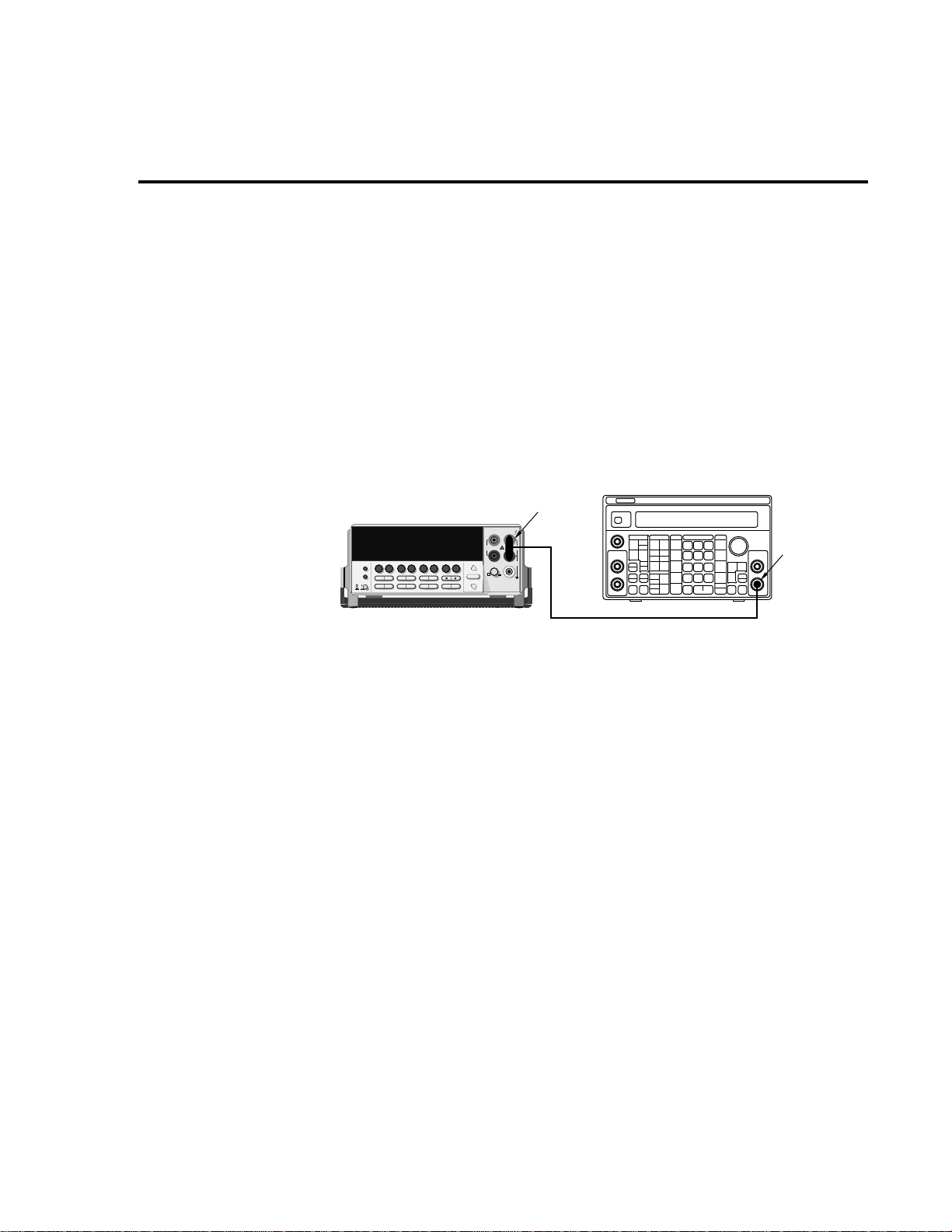
Front panel manufacturing calibration
1. Press in and hold the OPEN key while turning on the power.
2. Connect the low-thermal short to the rear panel input jacks, and select the rear inputs
with the INPUTS switch. Allow three minutes for thermal equilibrium.
3. Press SHIFT then CAL, select RUN, and then enter the appropriate calibration code (default: 002010).
4. Select ALL at the CAL:RUN prompt.
5. Press ENTER.
6. Perform the entire front panel comprehensive calibration procedure discussed earlier in
this section. (See Comprehensive calibration.)
7. Connect the synthesizer to the Model 2010 front panel INPUT jacks as shown in Figure
2-5. Select the front input jacks with the INPUTS switch.
Calibration 2-25
Figure 2-5
Synthesizer connections for manufacturing
calibration
Model 3930A or 3940 Synthesizer
50Ω BNC Coaxial Cable
Note: Synthesizer output voltage
must be accurately measured.
(See text).
Main
Function
Output
Model 2010
2000 MULTIMETER
!
R
BNC-to-Dual
Banana Plug
Adapter
8. After the last A C current calibration step, the instrument will prompt you to enter 3Hz at
1V RMS and 1kHz with the following prompts:
• Low-frequency cal: Set the synthesizer to output a 1V RMS, 3Hz sine w ave. Use the left
and right arrow keys and the range k eys to adjust the display to agree with the synthesizer
amplitude you measured previously, and then press ENTER.
• Frequency cal: Set the synthesizer to output a 1V RMS, 1kHz sine wave. Enter
1.000000kHz at the prompt, and then press ENTER.
9. Set the calibration dates, and then save calibration to complete the process.
Page 55

2-26 Calibration
Remote manufacturing calibration
1. Connect the low-thermal short to the rear panel input jacks, and select the rear inputs
with the INPUTS switch. Allow three minutes for thermal equilibrium.
2. Press in and hold the OPEN key while turning on the power.
3. Enable calibration by sending the :CODE command. For example, the def ault command
is:
:CAL:PROT:CODE 'KI002010'
4. Initiate calibration by sending the following command:
:CAL:PROT:INIT
5. Calibrate step 0 with the following command:
:CAL:PROT:AC:STEP0
6. Perform the entire SCPI command comprehensive calibration procedure discussed earlier in this section. (See Comprehensive calibration.)
7. Connect the synthesizer to the Model 2010 INPUT jacks as shown in Figure 2-5. Select
the front input jacks with the INPUTS switch.
8. Set the synthesizer to output a 1V RMS, 3Hz sine wave, and then send the following
command:
:CAL:PROT:AC:STEP14 <Cal_voltage>
<Cal_voltage> is the actual 3Hz synthesizer signal amplitude you measured pre viously.
9. Set the synthesizer to output a 1V RMS, 1kHz sine wave, and then send the following
command:
:CAL:PROT:AC:STEP15 1E3
10. Send the following commands to set calibration dates, sav e calibration, and lock out calibration:
:CAL:PROT:DATE <year>, <month>, <day>
:CAL:PROT:NDUE <year>, <month>,<day>
:CAL:PROT:SAVE
:CAL:PROT:LOCK
Page 56

3
Routine
Maintenance
Page 57

3-2 Routine Maintenance
Introduction
This section describes routine type maintenance that can be performed by the operator and
includes procedures for replacing both the line fuse and the amps fuse.
Setting the line voltage and replacing the line fuse
W ARNING Disconnect the line cord at the rear panel, and remove all test leads connect-
ed to the instrument (front and rear) before replacing the line fuse.
The power line fuse is located in the power module ne xt to the AC power receptacle (see Figure 3-1). If the line voltage must be changed or if the line fuse requires replacement, perform the
following steps:
1. Place the tip of a flat-blade screwdriv er into the po wer module by the fuse holder assembly (see Figure 3-1). Gently push in and turn to the left. Release pressure on the assembly, and its internal spring will push it out of the power module.
2. Remove the fuse, and replace it with the type listed in Table 3-1.
CAUTION For continued protection against fire or instrument damage, replace the fuse
only with the type and rating listed. If the instrument repeatedly blows fuses,
locate and correct the cause of the trouble before replacing the fuse.
3. If configuring the instrument for a different line voltage, remo ve the line voltage selector
from the assembly , and rotate it to the proper position. When the selector is installed into
the fuse holder assembly, the correct line voltage appears inverted in the window.
4. Install the fuse holder assembly into the power module by pushing it in until it locks in
place.
Page 58

WARNING:NO INTERNAL OPERATOR SERVICABLE PARTS,SERVICE BY QUALIFIED PERSONNEL ONLY.
WARNING:NO INTERNAL OPERATOR SERVICABLE PARTS,SERVICE BY QUALIFIED PERSONNEL ONLY.
CAUTION:FOR CONTINUED PROTECTION AGAINST FIRE HAZARD,REPLACE FUSE WITH SAME TYPE AND RATING.
CAUTION:FOR CONTINUED PROTECTION AGAINST FIRE HAZARD,REPLACE FUSE WITH SAME TYPE AND RATING.
Routine Maintenance 3-3
Figure 3-1
Power module
HI
350V
!
PEAK
LO
SENSE
Ω 4W
!
Table 3-1
Power line fuse
Line voltage Rating
Model 2010
MADE IN
TRIGGER
U.S.A.
LINK
RS232
!
VMC
EXT TRIG
!
FUSE LINE
250mAT
100 VAC
(SB)
120 VAC
220 VAC
125mAT
240 VAC
(SB)
1000V
PEAK
500V
3 5
1
PEAK
INPUT
4 6
2
IEEE-488
(CHANGE IEEE ADDRESS
FROM FRONT PANEL)
120
LINE RATING
50, 60
400HZ
17 VA MAX
Line Voltage Selector
Fuse
220
240
120
100
Spring
Window
Fuse Holder Assembly
Keithley part
no.
100/120V
220/240V
0.25A, slow-blow
0.125A, slow-blow
Note: 5 × 20mm fuses required
FU-96-4
FU-91
Page 59

3-4 Routine Maintenance
Replacing the AMPS fuse
The AMPS fuse protects the current input from an over-current condition. Follow the steps
below to replace the AMPS fuse.
WARNING Make sure the instrument is disconnected from the power line and other
equipment before replacing the AMPS fuse.
1. Turn off the power, and disconnect the power line and test leads.
2. From the front panel, gently push in the AMPS jack with your thumb, and rotate the fuse
carrier one-quarter turn counter-clockwise. Release pressure on the jack, and its internal
spring will push the fuse carrier out of the socket.
3. Remove the fuse, and replace it with the same type: 3A, 250V, fast blow, Keithley part
number FU-99-1.
CAUTION Do not use a fuse with a higher current rating than specified, or instrument
damage may occur. If the instrument repeatedly blows fuses, locate and correct the cause of the trouble before replacing the fuse.
4. Install the new fuse by reversing the above procedure.
Page 60

4
Troubleshooting
Page 61

4-2 Troubleshooting
Introduction
This section of the manual will assist you in troubleshooting and repairing the Model 2010.
Included are self-tests, test procedures, troubleshooting tables, and circuit descriptions. It is left
to the discretion of the repair technician to select the appropriate tests and documentation needed
to troubleshoot the instrument.
WARNING The information in this section is intended for qualified service personnel
only . Do not perform these procedures unless you are qualified to do so. Some
of these procedures may expose you to hazardous voltages that could cause
personal injury or death. Use caution when working with hazardous voltages.
Repair considerations
Before making any repairs to the Model 2010, be sure to read the following considerations.
CAUTION The PC boards are built using surface mount techniques and require special-
ized equipment and skills for repair. If you are not equipped and/or qualified,
it is strongly recommended that you send the unit back to the factory for repairs or limit repairs to the PC board replacement level. Without proper
equipment and training, you could damage a PC board beyond repair.
• Repairs will require various degrees of disassembly. However, it is recommended that
the Front Panel Tests be performed prior to any disassembly. The disassembly instructions for the Model 2010 are contained in Section 5 of this manual.
• Do not make repairs to surface mount PC boards unless equipped and qualified to do so
(see previous CAUTION).
• When working inside the unit and replacing parts, be sure to adhere to the handling precautions and cleaning procedures explained in Section 5.
• Many CMOS devices are installed in the Model 2010. These static-sensitive devices require special handling as explained in Section 5.
• Whenever a circuit board is removed or a component is replaced, the Model 2010 must
be recalibrated. See Section 2 for details on calibrating the unit.
Power-on self-test
During the power-on sequence, the Model 2010 will perform a checksum test on its EPROM
(U156 and U157) and test its RAM (U151 and U152). If one of these tests fails, the instrument
will lock up.
Page 62

Troubleshooting 4-3
Front panel tests
There are two front panel tests: one to test the functionality of the front panel keys and one to
test the display. In the event of a test failure, refer to Display board checks for details on troubleshooting the display board.
KEY test
The KEY test allows you to check the functionality of each front panel key. Perform the following steps to run the KEY test:
1. Press SHIFT and then TEST to access the self-test options.
2. Use the up or down RANGE key to display TEST: KEY.
3. Press ENTER to start the test. When a key is pressed, the label name for that key is displayed to indicate that it is functioning properly . When the ke y is released, the “NO KEY
PRESS” message is displayed.
4. Pressing EXIT tests the EXIT key. However, the second consecutive press of EXIT
aborts the test and returns the instrument to normal operation.
DISP test
rescent display is working properly. Perform the following steps to run the display test:
The display test allows you to verify that each segment and annunciator in the vacuum fluo-
1. Press SHIFT and then TEST to access the self-test options.
2. Use the up or down RANGE key to display TEST: DISP.
3. Press ENTER to start the test. There are four parts to the display test. Each time ENTER is pressed, the next part of the test sequence is selected. The four parts of the
test sequence are:
• All annunciators are displayed.
• The segments of each digit are sequentially displayed.
• The 12 digits (and annunciators) are sequentially displayed.
• The annunciators located at either end of the display are sequentially displayed.
4. When finished, abort the display test by pressing EXIT . The instrument returns to normal
operation.
Page 63

4-4 Troubleshooting
Principles of operation
The following information is provided to support the troubleshooting tests and procedures
covered in this section of the manual. Refer to the following block diagrams:
Figure 4-1 — Power supply block diagram
Figure 4-2 — Digital circuitry block diagram
Figure 4-3 — Analog circuitry block diagram
Power supply
The following information provides some basic circuit theory that can be used as an aid to
troubleshoot the power supply. A block diagram of the power supply is shown in Figure 4-1.
AC power is applied to the AC power module receptacle (J1009). Power is routed through the
line fuse and line voltage selection switch of the power module to the power transformer. The
power transformer has a total of four secondary windings for the various supplies.
AC voltage for the display fi laments is taken from a power transformer secondary at F1 and
F2, and then routed to the display board.
Each DC supply uses a rectifier and a capacitive filter , and man y supplies use an IC regulator .
Table 4-1 summarizes rectifier, filter, and regulator circuits for the various DC supplies.
Table 4-1
Power supply components
Supply Rectifier Filter Regulator
+5VD
+37V
+15V
-15V
+5V, +5VRL
+25V
-25V
+18V
-18V
+20V
CR104
CR116, CR117
CR102
CR102
CR103
CR136, CR140, CR141
CR137, CR138, CR139
CR102
CR102
–
C156, C175
C104
C148
C131
C146
C281
C284
–
–
C279, C281
U144
U101
U180
U179
U124
–
–
–
–
U187
Page 64

Troubleshooting 4-5
Figure 4-1
Power supply
block diagram
Fuse
Power
Switch
Line
Voltage
Switch
Power
Transformer
CR104
C175, C156
U144
CR116, CR117
C108
U101
CR102
C131, C148
U179, U180
CR103
C146
U124
CR102, CR136
CR137, CR138
CR139, CR140
CR141, C281
C284
+5VD
D Common
+37V
D Common
+15V
A Common
-15V
+5V, +5VRL
A Common
+18V
A Common
-18V
-25V
A Common
+25V
U187
C279
C281
+20V
A Common
Page 65

4-6 Troubleshooting
Display board
Display board components are shown in the digital circuitry block diagram in Figure 4-2.
Microcontroller
U401 is the display board microcontroller that controls the display and interprets key data.
The microcontroller uses three internal peripheral I/O ports for the various control and read
functions. Display data is serially transmitted to the microcontroller from the digital section via
the TXB line to the microcontroller RDI terminal. In a similar manner, key data is serially sent
back to the digital section through the RXB line via TDO. The 4MHz clock for the microcontroller is generated by crystal Y401.
Display
DS401 is the display module, which can display up to 12 alphanumeric characters and includes the various annunciators.
The display uses a common multiplexing scheme with each character refreshed in sequence.
U402 and U403 are the drivers for the display characters and annunciators. Note that data for
the drivers is serially transmitted from the microcontroller (MOSI and PC1).
Filament voltage for the display is derived from the power supply transformer (F1 and F2).
The display drivers require +37VDC and +5VDC, which are supplied by U144 (+5VD) and
U101 (+37V).
Key matrix
The front panel keys (S401-S430) are organized into a row-column matrix to minimize the
number of microcontroller peripheral lines required to read the keyboard. A k ey is read by strobing the columns and reading all rows for each strobed column. K e y-do wn data is interpreted by
the display microcontroller and sent back to the main microprocessor using proprietary encoding schemes.
Digital circuitry
Refer to Figure 4-2 for the following discussion on digital circuitry.
Microprocessor
U135 is a 68306 microprocessor that oversees all operating aspects of the instrument. The
MPU has a 16-bit data bus and provides an 18-bit address b us. It also has parallel and serial ports
for controlling various circuits. For example, the RXDA, TXDA, RXDB and TXDB lines are
used for the RS-232 interface.
The MPU clock frequency of 14.7456MHz is controlled by crystal Y101.
Page 66

Troubleshooting 4-7
Figure 4-2
Digital circuitry
block diagram
Analog
Circuitry
(See Figure 4-3)
XADTX
XADCLK
XADTS
XADRX
Scan Control
Memory circuits
O
O
O
AT101
U150
U155
Trigger
U146, U164
Trigger
Link
P
T
I
S
NVRAM
U136
ADTX
ADCLK
ADTS
ADRXB
TRIG IN
TRIG OUT
ROM
U156, U157
68306
µP
U135
U151, U152
IN
OUT
Data IN
Data OUT
RAM
RS-232
U158, U160,
Display Board
Controller
U401
XTAL
Y101
U159
GPIB
U161
Keypad
Display
DS401
RS-232
Port
IEEE-488
Bus
ROMs U156 and U157 store the firmware code for instrument operation. U157 stores the D0-
D7 bits of each data word, and U156 stores the D8-D15 bits.
RAMs U151 and U152 provide temporary operating storage. U152 stores the D0-D7 bits of
each data word, and U151 stores the D8-D15 bits.
Semi-permanent storage facilities include NVRAM U136. This IC stores such information as
instrument setup and calibration constants. Data transmission from this device is performed serially.
RS-232 interface
Serial data transmission and reception is performed by the TXDB and RXDB lines of the
MPU. U159 provides the necessary voltage level conversion for the RS-232 interface port.
IEEE-488 interface
U158, U160, and U161 make up the IEEE-488 interface. U158, a 9914A GPIA, takes care of
routine bus overhead such as handshaking, while U160 and U161 provide the necessary buffering and drive capabilities.
Page 67

4-8 Troubleshooting
T rigger circuits
Buffering for Trigger Link input and output is performed by U146. T rigger input and output
is controlled by the IRQ4 and PB3 lines of the MPU. U164 provides additional logic for the trigger input to minimize MPU control overhead.
At the factory, trigger output is connected to line 1 of the Trigger Link connector (resistor
R267 installed). Trigger input is connected to line 2 of the T rigger Link connector (resistor R270
installed).
Analog circuitry
Refer to Figure 4-3 for the following discussion on analog circuitry.
Figure 4-3
Analog circuitry
block diagram
AMPS
INPUT
HI
R117, Q109,
Q114, Q136
SENSE
HI
SENSE
LO
Scanner Output
Scanner
Inputs
Current Shunts
Q165, Q164, K103,
R158, R205, R386,
Q101, Q102
DCV
Divider
DCV/100
R373, Q121, Q135
Scanner
Option
*Solid State Protection
R450
K101
SSP*
Protection
DCA
ACA
AC Switching
&
Gain
K102, U102, U103, U105,
U112, U118, U111, U110
ACV,
FREQ
DCV
OHMS
SSP
Q153, CR132
Ohms I-Source
U133, Q123, Q125,
Q124, Q126, Q119,
Q166, U123
Scanner Control
DCV & Ohms
Switching
Q104, Q105,
Q108, Q113
X1
Buffer
Q137,
Q138,
U166,
U167
BUFCOM
A/D
MUX &
Gain
U163, U177,
U176, Q156
ADC
U165
Digital
Circuitry
(See Figure 4-2)
INPUT HI
INPUT HI protection is provided by the SSP (solid state protection) circuit. The SSP is primarily made up of Q101 and Q102. An overload condition opens Q101 and Q102, which disconnects the analog input signal from the rest of the analog circuit.
Note that for the 100VDC and 1000VDC ranges, Q101 and Q102 of the SSP are open. The
DC voltage signal is routed through the DCV Divider (Q114 and Q136) to the DCV switching
circuit.
Page 68

Troubleshooting 4-9
AMPS input
The ACA or DCA input signal is applied to the Current Shunt circuit, which is made up of
K103, Q165, Q164, R205, R450, R386, and R158. U178 controls if either Q164 or Q165 is
turned on. For the 3A and 1A DCA ranges and all ACA ranges, 0.1
the input (K103 off). For the 100mA DCA range, K103 is ener gized (on). Q164 (both) are turned
on with the LOAMP control line set high. 1.01
the 10mA DCA range, K103 is energized (on). Q165 (both) are turned on with the LO AMP control line set low. 10.1
The A CA signal is then sent to the A C Switching & Gain circuit, while the DCA signal is routed directly to the A/D MUX & Gain circuit.
Ω (R205//R450 + R386 + R158) is shunted across the input.
Ω (R386 + R158) is shunted across the input. For
Ω (R158) is shunted across
Signal switching
Signal switching for DCV and OHMS is done by the DCV & Ohms Switching circuit. FETs
Q113, Q105, Q104, and Q108 connect the DCV or ohms signal to the X1 buf fer (Q137, U167,
and U166). (See Analog signal switching states at the end of this section for a summary of
switching states of these FETs for the various DCV and OHMS ranges.)
Note that the reference current for OHMS is generated by the Ohms I-Source circuit. For 4wire ohms measurements, SENSE LO is connected to the circuit by controlling U163.
Signal switching and gain for ACV, FREQ, and ACA is done by the AC Switching & Gain
circuit, which is primarily made up of K102, U102, U103, U105, U112, U118, U111, and U110.
(See Analog signal switching states.) Note that U111 is used for frequency adjustment. The
states of these analog switches vary from range to range.
Multiplexer and A/D converter
All input signals, except FREQ, are routed to the A/D MUX & Gain circuit. The multiplexer
(U163) switches the various signals for measurement. In addition to the input signal, the multiplexer also switches among reference and zero signals at v arious phases of the measurement c ycle.
When the input signal is selected by the MUX, it is amplified by a composite operational amplifier made up of Q156 and U177. Tables in Analog signal switching states at the end of this
section provide the switch states of U176, which determine the gain for Q156 and U177.
The multiplexed signals of the measurement cycle are routed to the A/D Converter (U165),
where it converts the analog signals to digital form. The digital signals are then routed through
an opto-isolator to the MPU to calculate a reading.
Page 69

4-10 Troubleshooting
T roubleshooting
Troubleshooting information for the v arious circuits is summarized below. See Analog signal
switching states for additional information regarding the analog circuitry.
Display board checks
If the front panel DISP test indicates that there is a problem on the display board, use Table
4-2. See Principles of operation for display circuit theory.
Table 4-2
Display board checks
Step Item/component Required condition Remarks
1
Front panel DISP test.
2
P1005, pin 5
3
P1005, pin 9
4
U401, pin 1
5
U401, pin 43
6
U401, pin 32
7
U401, pin 33
Verify that all segments operate.
+5V ±5%
+37V ±5%
Goes low briefly on power up,
then goes high.
4MHz square wave.
Pulse train every 1ms.
Brief pulse train when front
panel key is pressed.
Use front panel display test.
Digital +5V supply.
Display +37V supply.
Microcontroller RESET.
Controller 4MHz clock.
Control from main processor.
Key down data sent to main
processor.
Page 70

Power supply checks
Power supply problems can be checked using Table 4-3. See Principles of operation for circuit theory on the power supply.
Table 4-3
Power supply checks
Step Item/component Required condition Remarks
Troubleshooting 4-11
Line fuse
1
Line voltage
2
Line power
3
U144, pin 2
4
U101, pin 7
5
U180, pin 3
6
U179, pin 3
7
U124, pin 3
8
CR141 cathode
9
CR139 anode
10
U180, pin 1
11
U179, pin 2
12
Q183, emitter
13
Check continuity.
120V/240V as required.
Plugged into live receptacle, power on.
+5V ±5%
+37V ±5%
+15V ±5%
-15.7V ±5%
+5V ±5%
+25V ± 20%
-25V ±20%
+18V ±20%
-18V ±20%
+21V ±5%
Remove to check.
Check power module position.
Check for correct power-up
sequence.
+5VD, referenced to Common D.
+37V, referenced to Common D.
+15V, referenced to Common A.
-15V, referenced to Common A.
+5VRL, referenced to Common A.
+25V, referenced to Common A.
-25V, referenced to Common A.
+18V, referenced to Common A.
-18V, referenced to Common A.
+20V, referenced to Common A.
Page 71

4-12 Troubleshooting
Digital circuitry checks
Digital circuit problems can be checked using Table 4-4. See Principles of operation for a dig-
ital circuit description.
Table 4-4
Digital circuitry checks
Step Item/component Required condition Remarks
Power-on test
1
U157 pin 16
2
U157 pin 32
3
U135 pin 48
4
U135, lines A1-A23
5
U135, lines D1-D15
6
U135 pin 44
7
U159 pin 13
8
U159 pin 14
9
U158 pins 34-42
10
U158 pins 26-31
11
U158 pin 24
12
U158 pin 25
13
U135 pin 84
14
U135 pin 91
15
U135 pin 90
16
U135 pin 89
17
RAM OK, ROM OK.
Digital common.
+5V
Low on power-up, then goes
high.
Check for stuck bits.
Check for stuck bits.
14.7456MHz
Pulse train during RS-232 I/O.
Pulse train during RS-232 I/O.
Pulse train during IEEE-488 I/O.
Pulses during IEEE-488 I/O.
Low with remote enabled.
Low during interface clear.
Pulse train.
Pulse train.
Pulse train.
Pulse train.
Verify that RAM and ROM are
functional.
All signals referenced to digital
common.
Digital logic supply.
MPU RESET line.
MPU address bus.
MPU data bus.
MPU clock.
RS-232 RX line.
RS-232 TX line.
IEEE-488 data bus.
IEEE-488 command lines.
IEEE-488 REN line.
IEEE-488 IFC line.
ADRXB
ADTX
ADCLK
ADTS
Page 72

Analog signal switching states
Tables 4-5 through 4-11 provide switching states of the various relays, FETs, and analog
switches for the basic measurement functions and ranges. These tables can be used to assist in
tracing an analog signal from the input to the A/D multiplexer.
Table 4-5
DCV signal switching
Range Q101 Q102 Q114 Q136 Q109 K101* Q113 Q105 Q104 Q108
OFF
OFF
OFF
ON
100mV
1V
10V
100V
1000V
ON
ON
ON
OFF
OFF
ON
ON
OFF
OFF
OFF
OFF
ON
ON
OFF
OFF
ON
ON
OFF
OFF
OFF
OFF
SET
SET
SET
SET
SET
Troubleshooting 4-13
OFF
ON
ON
OFF
OFF
ON
ON
OFF
OFF
ON
OFF
OFF
ON
OFF
OFF
OFF
ON
OFF
OFF
OFF
Sense
volts Q154 Q153
100mV
1V
10V
*K101 SET states: Pin 8 switched to Pin 7
OFF
OFF
OFF
OFF
OFF
OFF
OFF
OFF
OFF
Pin 3 switched to Pin 4
OFF
OFF
OFF
OFF
OFF
OFF
SET
SET
SET
ON
ON
ON
OFF
OFF
OFF
OFF
OFF
OFF
ON
ON
ON
OFF
OFF
OFF
Table 4-6
ACV and FREQ signal switching
Range Q101 Q102 K101* K102*
100mV
1V
10V
100V
750V
*K101 and K102 RESET states: Pin 8 switched to Pin 9
K101 and K102 SET states: Pin 8 switched to Pin 7
ON
ON
ON
ON
ON
ON
ON
ON
ON
ON
RESET
RESET
RESET
RESET
RESET
RESET
RESET
SET
SET
SET
Pin 3 switched to Pin 2
Pin 3 switched to Pin 4
U103
pin 8
ON
ON
OFF
OFF
OFF
U103
pin 9
ON
ON
OFF
OFF
OFF
U105
pin 9
OFF
OFF
ON
ON
ON
U105
pin 8
OFF
OFF
OFF
OFF
ON
U103
pin 16
OFF
ON
OFF
ON
OFF
U103
pin 1
ON
OFF
ON
OFF
OFF
U105
pin 1
ON
OFF
ON
OFF
OFF
ON
ON
ON
U111
pin 16
OFF
OFF
OFF
OFF
OFF
Page 73

4-14 Troubleshooting
Table 4-7
Ω
2 signal switching
Range K104 Q101 Q102 Q114 Q136 Q109 K101* K102* Q113 Q105 Q104 Q108 Q153 Q167
OFF
ON
OFF
OFF
ON
10 Ω
100 Ω
1k Ω
10k Ω
100k Ω
1M Ω
10M Ω
100M Ω
*K101 set states: Pin 8 switched to Pin 7
K102 reset states: Pin 8 switched to Pin 9
RESET
RESET
RESET
RESET
RESET
RESET
RESET
RESET
ON
OFF
ON
ON
OFF
ON
ON
OFF
ON
ON
OFF
ON
ON
OFF
ON
ON
OFF
ON
ON
OFF
ON
ON
Pin 3 switched to Pin 4
Pin 3 switched to Pin 2
OFF
ON
OFF
OFF
OFF
OFF
OFF
OFF
OFF
OFF
OFF
OFF
OFF
OFF
OFF
OFF
ON
ON
SET
SET
SET
SET
SET
SET
SET
SET
RESET
RESET
RESET
RESET
RESET
RESET
SET
SET
OFF
OFF
OFF
OFF
OFF
OFF
OFF
OFF
ON
ON
ON
ON
ON
ON
ON
OFF
OFF
OFF
OFF
OFF
OFF
OFF
OFF
OFF
OFF
OFF
OFF
OFF
OFF
ON
ON
ON
ON
ON
OFF
OFF
OFF
OFF
OFF
OFF
OFF
OFF
OFF
Table 4-8
Ω
4 signal switching
Range K104
10 Ω
100 Ω
1k Ω
10k Ω
100k Ω
1M Ω
10M Ω
100M Ω
RESET
RESET
RESET
RESET
RESET
RESET
RESET
RESET
Q101Q102Q114Q136Q10
OFF
OFF
OFF
OFF
OFF
OFF
OFF
OFF
OFF
OFF
OFF
OFF
OFF
OFF
OFF
OFF
OFF
OFF
OFF
ON
ON
OFF
ON
ON
Dry
circuit
10 Ω
100 Ω
*K101 set states: Pin 8 switched to Pin 7
SET
SET
K102 reset states: Pin 8 switched to Pin 9
OFF
OFF
OFF
OFFONONONON
Pin 3 switched to Pin 4
Pin 3 switched to Pin 2
OFF
OFF
OFF
OFF
OFF
OFF
OFF
OFF
9
OFF
OFF
OFF
OFF
OFF
OFF
ON
ON
OFF
OFF
K101* K102*
SET
SET
SET
SET
SET
SET
SET
SET
RESET
RESET
RESET
RESET
RESET
RESET
RESET
RESET
SET
SET
RESET
RESETONON
Q113Q105Q104Q108Q153Q16
7
OFF
ON
OFF
OFF
OFF
ON
OFF
ON
OFF
OFF
OFF
ON
OFF
ON
OFF
OFF
OFF
ON
OFF
ON
OFF
OFF
OFF
ON
OFF
ON
OFF
OFF
OFF
ON
OFF
ON
OFF
OFF
OFF
ON
OFF
OFF
OFF
OFF
ON
OFF
OFF
OFF
OFF
OFF
ON
OFF
OFF
OFF
OFF
OFF
OFF
OFFONONONON
Page 74

Table 4-9
Ω
2/
Ω
4 reference switching
Range U133 pin 8 U133 pin 1 Q123 Q125 Q124 Q126
Troubleshooting 4-15
10 Ω
100 Ω
1k Ω
10k Ω
100k Ω
1M Ω
10M Ω
100M Ω
Dry
circuit
10 Ω
100 Ω
Table 4-10
DCA signal switching
Range K103 Q165 Q164
10mA
100mA
1A
3A
OFF
ON
ON
OFF
ON
ON
OFF
OFF
ON
OFF
ON
ON
OFF
OFF
ON
OFF
OFF
ON
OFF
OFF
ON
ON
OFF
ON
ON
OFF
OFF
OFF
ON
ON
ON
OFF
OFF
OFF
OFF
OFF
ON
OFFONOFF
OFF
ON
ON
ON
ON
ON
ON
OFF
OFF
OFF
OFF
OFF
OFF
OFF
OFF
ON
ON
ON
ON
ON
OFFONOFF
OFF
OFF
OFF
ON
ON
ON
ON
ON
ON
Table 4-11
ACA signal switching
Range K103
1A
3A
(U163) to the final amplifier stage. These tables show the MUX lines (S3, S4, S6, S7) that are
selected for measurement during the SIGNAL phase of the multiplexing cycle. Also included
are switching states of analog switches (U176) that set up the gain for the final amplifier stage
(U177).
OFF
OFFONONONON
T ables 4-12 through 4-16 can be used to trace the analog signal through the A/D multiplexer
U105
pin 16
U105
pin 1
U111
pin 16
OFFONOFF
U105
pin 8
OFF
U103
pin 16
OFF
OFF
U103
pin 1
OFF
OFF
Page 75

4-16 Troubleshooting
Table 4-12
DCV signal multiplexing and gain
Range
100mV
1V
10V
100V
1000V
Table 4-13
ACV and ACA signal multiplexing and gain
Range
All ON ON OFF X1 OFF
Table 4-14
DCA signal multiplexing and gain
Range
10mA
100mA
1A
3A
Signal
(U163)
S4
S4
S4
S4
S4
U176
pin 1
Signal
(U163)
S6
S6
S6
S6
U176
pin 1
OFF
OFF
OFF
OFF
OFF
U176
pin 8
U176
pin 1
OFF
OFF
OFF
OFF
U176
pin 8
OFF
OFF
ON
OFF
ON
U176
pin 9
U176
pin 8
OFF
OFF
OFF
OFF
U176
pin 9
OFF
ON
OFF
ON
OFF
Gain
(U177)
U176
pin 9
OFF
OFF
OFF
ON
Gain
(U177)
X100
X10
X1
X10
X1
U129
pin 1
Gain
(U177)
X100
X100
X100
X10
U129
pin 16
ON
OFF
OFF
OFF
OFF
U176
pin 16
ON
ON
ON
OFF
Page 76

Table 4-15
Ω
2 signal multiplexing and gain
Troubleshooting 4-17
Range
10Ω
100Ω
1kΩ
10kΩ
100kΩ
1MΩ
10MΩ
100MΩ
Signal
(U163)
S4
S4
S4
S4
S4
S4
S4
S4
U176
pin 1
OFF
OFF
OFF
OFF
OFF
OFF
OFF
OFF
Table 4-16
Ω
4 signal multiplexing and gain
Range
10Ω
100Ω
1kΩ
10kΩ
100kΩ
1MΩ
10MΩ
100MΩ
Signal
(U163)
S4 then S7
S4 then S7
S4 then S7
S4 then S7
S4 then S7
S4 then S7
S4 then S7
S4 then S7
U176
pin 1
OFF
OFF
OFF
OFF
OFF
OFF
OFF
OFF
U176
pin 8
OFF
OFF
OFF
OFF
OFF
ON
ON
ON
U176
pin 8
OFF
OFF
OFF
OFF
OFF
ON
ON
ON
U176
pin 9
OFF
OFF
ON
ON
ON
OFF
OFF
OFF
U176
pin 9
OFF
OFF
ON
ON
ON
OFF
OFF
OFF
Gain
(U177)
X100
X100
X10
X10
X10
X1
X1
X1
Gain
(U177)
X100
X100
X10
X10
X10
X1
X1
X1
U176
pin 16
ON
ON
OFF
OFF
OFF
OFF
OFF
OFF
U176
pin 16
ON
ON
OFF
OFF
OFF
OFF
OFF
OFF
Figure 4-3 provides a block diagram of the analog circuitry. Table 4-17 is provided to show
where the various switching devices are located in the block diagram.
Table 4-17
Circuit section locations for switching devices
Switching devices
Q101, Q102, Q153
Q114, Q136, Q109
K101, Q113, Q105, Q104, Q108, Q167
K102, U103, U105, U111
U133, Q123, Q125, Q124, Q126, Q120
K103, Q164, Q165
U163, U177, U176
Analog circuit section
(see Figure 4-3)
SSP (Solid State Protection)
DCV Divider
DCV & Ohms Switching
AC Switching & Gain
Ohms I-Source
Current Shunts
A/D Mux & Gain
Page 77

4-18 Troubleshooting
No comm link error
A “No Comm Link” error indicates that the front panel processor has ceased communication
with the main processor, which is located on the mother board. This error indicates that there
may be a problem with the cable connection from the front panel display or one of the main processor ROMs may require re-seating in its socket. Check to be sure there is a proper cable connection from the front panel display. ROMs may be reseated as follows:
1. Turn of f the po wer, and disconnect the line cord and all other test leads and cables from
the instrument.
2. Remove the case cover as outlined in Section 5.
3. Find the two firmware ROMs, U156 and U157, located on the mother board. These are
the only ICs installed in sockets. (Refer to the component layout drawing at the end of
Section 6 for exact locations.)
4. Carefully push down on each ROM IC to make sure it is properly seated in its socket.
CAUTION Be careful not to push down excessively, or you might crack the mother
board.
5. Connect the line cord, and turn on the power. If the problem persists, additional troubleshooting will be required.
Page 78

5
Disassembly
Page 79

5-2 Disassembly
Introduction
This section explains how to handle, clean, and disassemble the Model 2010 Multimeter. Dis-
assembly drawings are located at the end of this section.
Handling and cleaning
T o av oid contaminating PC board traces with body oil or other foreign matter , av oid touching
the PC board traces while you are repairing the instrument. Motherboard areas covered by the
shields have high-impedance de vices or sensitiv e circuitry where contamination could cause degraded performance.
Handling PC boards
Observe the following precautions when handling PC boards:
• Wear cotton gloves.
• Only handle PC boards by the edges and shields.
• Do not touch any board traces or components not associated with repair.
• Do not touch areas adjacent to electrical contacts.
• Use dry nitrogen gas to clean dust off PC boards.
Solder repairs
Observe the following precautions when soldering a circuit board:
• Use an OA-based (organic activated) flux, and take care not to spread the flux to other
areas of the circuit board.
• Remove the flux from the work area when you ha ve finished the repair by using pure water with clean, foam-tipped swabs or a clean, soft brush.
• Once you have removed the flux, swab only the repair area with methanol, then blowdry the board with dry nitrogen gas.
• After cleaning, allow the board to dry in a 50°C, lo w-humidity environment for several
hours.
Page 80

Disassembly 5-3
Static sensitive devices
CMOS devices operate at very high impedance le vels. Therefore, an y static that b uilds up on
you or your clothing may be sufficient to destroy these de vices if the y are not handled properly.
Use the following precautions to avoid damaging them.
CAUTION Many CMOS devices are installed in the Model 2010. Handle all semicon-
ductor devices as being static sensitive.
• Transport and handle ICs only in containers specially designed to prevent static buildup. Typically, you will receive these parts in anti-static containers made of plastic or
foam. Keep these devices in their original containers until ready for installation.
• Remove the devices from their protective containers only at a properly grounded work
station. Also, ground yourself with a suitable wrist strap.
• Handle the devices only by the body; do not touch the pins.
• Ground any printed circuit board into which a semiconductor device is to be inserted to
the bench or table.
• Use only anti-static type desoldering tools.
• Use only grounded-tip solder irons.
• Once the device is installed in the PC board, it is normally adequately protected, and you
can handle the boards normally.
Page 81

5-4 Disassembly
Assembly drawings
Use the following assembly drawings to assist you as you disassemble and re-assemble the
Model 2010. Also, refer to these drawings for information about the Keithley part numbers of
most mechanical parts in the unit. The drawings are located at the end of this section.
• Front Panel Assembly — 2010-040
• Chassis/Transformer Power Module Assembly — 2010-050
• Front Panel/Chassis Assembly — 2010-051
• Chassis Assembly — 2010-052
Page 82

Case cover removal
Follow the steps below to remove the case cover to gain access to internal parts.
WARNING Before removing the case cover, disconnect the line cord and any test leads
1. Remove Handle — The handle serves as an adjustable tilt-bail. Adjust its position by
gently pulling it away from the sides of the instrument case and swinging it up or do wn.
To remove the handle, swing the handle below the bottom surface of the case and back
until the orientation arrows on the handles line up with the orientation arrows on the
mounting ears. W ith the arro ws lined up, pull the ends of the handle a way from the case.
2. Remove Mounting Ears — Remov e the screw that secures each mounting ear . Pull do wn
and out on each mounting ear.
Disassembly 5-5
from the instrument.
NOTE When re-installing the mounting ears, make sure to mount the right ear to the right
side of the chassis, and the left ear to the left side of the chassis. Eac h ear is marked
“RIGHT” or “LEFT” on its inside surface.
3. Remove Rear Bezel — To remove the rear bezel, loosen the two captive screws that secure the rear bezel to the chassis. Pull the bezel away from the case.
4. Removing Grounding Screws — Remo ve the two grounding scre ws that secure the case
to the chassis. They are located on the bottom of the case at the back.
5. Remove Cover — To remove the case, grasp the front bezel of the instrument, and carefully slide the chassis forward. Slide the chassis out of the metal case.
NOTE T o gain access to the components under the motherboar d shields, r emo ve the shields,
which are secured to the motherboard by their appropriate screw.
Page 83
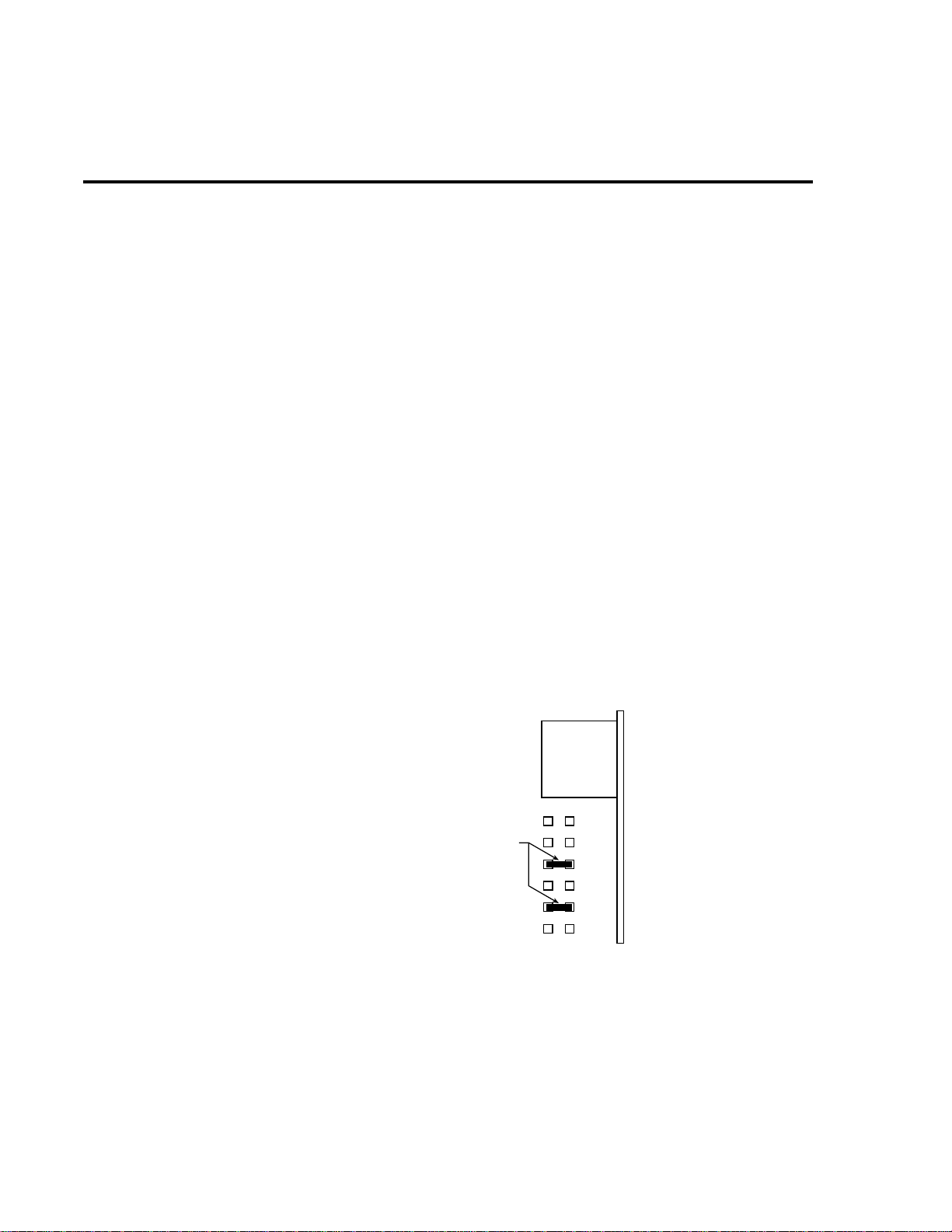
5-6 Disassembly
Changing trigger link lines
The Model 2010 uses two lines of the T rigger Link rear panel connector as External Trigger
(EXT TRIG) input and Voltmeter Complete (VMC) output. At the factory, line 1 is configured
as VMC and line 2 as EXT TRIG.
NOTE Line 1, 3, or 5 of the T rigger Link can be confi gur ed as VMC, while line 2, 4, or 6 can
be configured as EXT TRIG.
You can change trigger link line configurations by moving the position of resistors inside the
unit. Perform the following steps to change trigger link lines:
WARNING Make sure the instrument is disconnected from the power line and other
equipment before performing the following procedure.
Figure 5-1
Trigger link connectors
1. Remove the cover from the instrument as explained in Case cover removal.
2. The resistors used to select the trigger link lines are located next to the T rigger Link connector as shown in Figure 5-1. The “resistors” are actually solder beads that bridge pcboard pads. If the factory default lines are selected, the solder beads will be located at
R270 (line 2, EXT TRIG) and R267 (line 1, VMC).
3. To change a trigger link line:
• Use a hot air pencil to remove the appropriate solder bead.
• Using a solder with OA-based flux, apply a solder bead to the appropriate resistor
location.
• Replace the cover on the instrument.
Mother Board
(view from top)
Trigger Link Lines
Line 1 = VMC (R267)
Line 2 = EXT TRIG (R270)
Line 3 = VMC (R266)
Line 4 = EXT TRIG (R268)
Line 5 = VMC (R265)
Line 6 = EXT TRIG (R269)
Solder
Bead
Trigger Link
Connector
R269
R268
R270
R265
R267
R266
Rear Panel
Page 84

Motherboard removal
Perform the following steps to remov e the motherboard. This procedure assumes that the case
cover is already removed.
1. Remove the IEEE-488 and RS-232 fasteners.
The IEEE-488 and the RS-232 connectors each have two nuts that secure the connectors
to the rear panel. Remove these nuts.
2. Remove the front/rear switch rod.
At the switch, place the edge of a flat-blade screw driver in the notch on the pushrod.
Gently twist the screw driver while pulling the rod from the shaft.
3. Disconnect the front and rear input terminals.
You must disconnect these input terminal connections for both the front and rear inputs:
• INPUT HI and LO
• SENSE HI and LO
• AMPS
Disassembly 5-7
Remove all the connections except the front AMPS connection by pulling the wires off the
pin connectors. T o remov e the front panel AMPS input wire (white), first remove the AMPS fuse
holder, and then use needle-nose pliers to grasp the AMP wire near fuse housing. Push the wire
forward and down to snap the spring out of the fuse housing. Carefully pull the spring and contact tip out of housing.
During re-assembly, use the following table to identify input terminals:
Input terminals Front wire color Rear wire color
INPUT HI
INPUT LO
SENSE HI
SENSE LO
AMPS
4. Unplug cables:
• Unplug the display board ribbon cable from connector J1014.
• Unplug the transformer cables from connectors J1016 and J1015.
• Unplug the OPTION SLOT ribbon cable from connector J1017.
5. Remove the fastening scre w that secures the main PC board to the chassis. This scre w is
located along the left side of the unit towards the rear. It also holds down U144.
During re-assembly, replace the board, and start the IEEE-488 and RS-232 connector
nuts and the mounting screw. T ighten all the f asteners once they are all in place and the
board is correctly aligned.
6. Remove the motherboard, which is held in place by edge guides on each side, by sliding
it forward until the board edges clear the guides. Carefully pull the motherboard from
the chassis.
Red
Black
Yellow
Gray
White
White/Red
White/Black
White/Yellow
White/Gray
—
Page 85

5-8 Disassembly
Front panel disassembly
Use the following procedures to remov e the display board and/or the pushbutton switch pad:
NOTE You must first remove the case cover, the front/rear input switch, and the front input
terminal wires as described in earlier in this section.
1. Unplug the display board ribbon cable from connector J1014.
2. Remove the front panel assembly.
This assembly has four retaining clips that snap onto the chassis over four pem nut studs.
Two retaining clips are located on each side of the front panel. Pull the retaining clips
outward and at the same time pull the front panel assembly forward until it separates
from the chassis.
3. Using a thin-bladed screw driv er , pry the plastic PC board stop (located at the bottom of
the display board) until the bar separates from the casing. Pull the display board from the
front panel.
4. Remove the switch pad by pulling it from the front panel.
Page 86

Main CPU firmware replacement
Changing the firmware may be necessary as upgrades become available. The firmware revision levels for the main and front panel CPUs are displayed during the po wer-on sequence. (The
main firmware revision level is displayed on the left; the front panel firmware revision level is
displayed on the right.) For example, REV: A01 A02 indicates a main firmw are revision le v el of
A01 and a front panel firmware revision level of A02.
The firmware for the main CPU is located in the EPROMs U156 (EVEN) and U157 (ODD),
leadless ICs that reside in chip carriers on the PC board. To replace the CPU firmware, perform
the following:
WARNING Disconnect the instrument from the power lines, and remove the test leads
before changing the firmware.
Disassembly 5-9
1. Remove the case cover as described earlier in this section.
2. Locate U156 EVEN and U157 ODD (EPROMs) on the main PC board. They are the
only devices installed in chip carriers (sockets).
CAUTION EPROMs U156 and U157 are static-sensitive devices. Be sure to follow the
handling precautions explained in Static sensitive devices.
3. Using an appropriate chip extractor, remove U156 from its chip carrier.
4. Position the new U156 EPROM on the appropriate chip carrier. Make sure the notched
corner of the chip is aligned with the notch in the chip carrier.
NOTE Be sure to install the correct EPROMs at the ODD and EVEN locations. The instru-
ment will not function if the EPROMs are installed in the wrong sockets.
5. With the EPROM properly positioned, push down on the chip until it completely seats
into the chip carrier.
6. Repeat steps 3 through 5 for EPROM U157.
7. After installation, make sure the instrument powers up normally before replacing the
cover.
Page 87

5-10 Disassembly
Removing power components
The following procedures for removing the po wer transformer and/or power module require
that the case cover and motherboard be removed, as previously explained.
Power transformer removal
Perform the following steps to remove the power transformer:
1. Remove motherboard.
2. Unplug the transformer wires that attach to the power module at the rear panel.
During re-assembly, use drawing 2010-050 as a reference and replace the wires as fol-
lows:
Top wire: Gray
Right top: Violet
Right bottom: White
Left top: Red
Left bottom: Blue
3. Remove the two nuts that secure the transformer to the bottom of the chassis.
4. Pull the black ground wire off the threaded stud, and remov e the power transformer from
the chassis.
WARNING To avoid electrical shock, which could result in injury or death, the black
ground wire of the transformer must be connected to chassis ground. When
installing the power transformer , be sure to re-connect the black ground wire
to the mounting stud on bottom of the chassis.
Page 88

Power module removal
Perform the following steps to remove the power module:
1. Remove motherboard.
2. Unplug the transformer wires that attach to the power module at the rear panel.
During re-assembly, use drawing 2010-050 as a reference, and replace the wires as fol-
lows:
Top wire: Gray
Right top: Violet
Right bottom: White
Left top: Red
Left bottom: Blue
Disassembly 5-11
3. Disconnect the power module's ground wire. This green and yellow wire connects to a
threaded stud on the chassis with a kep nut.
4. Squeeze the latches on either side of the power module while pushing the module from
the access hole.
WARNING To avoid electrical shock, which could result in injury or death, the ground
wire of the power module must be connected to chassis ground. When installing the power module, be sure to re-connect the green and yellow ground wire
to the threaded stud on the chassis.
Page 89

5-12 Disassembly
Instrument re-assembly
Re-assemble the instrument by reversing the previous disassembly procedures. Make sure
that all parts are properly seated and secured and that all connections are properly made. To ensure proper operation, replace and securely fasten the shield.
WARNING To ensure continued protection against electrical shock, verify that power
line ground (green and yellow wire attached to the power module) and the
power transformer ground (black wire) are connected to the chassis.
Page 90

6
Replaceable
Parts
Page 91

6-2 Replaceable Parts
Introduction
This section contains replacement parts information and component layout drawings for the
Model 2010.
Parts lists
The electrical parts lists for the Model 2010 are shown in Tables 4-1 to 4-3. For part numbers
to the various mechanical parts and assemblies, use the Miscellaneous parts list and the assembly drawings provided at the end of Section 5 and Tables 6-1 through 6-4.
Ordering information
T o place an order, or to obtain information concerning replacement parts, contact your Keithley
representative or the factory (see inside front co v er for addresses). When ordering parts, be sure to
include the following information:
• Instrument model number (Model 2010)
• Instrument serial number
• Part description
• Component designation (if applicable)
• Keithley part number
Page 92

Replaceable Parts 6-3
Factory service
If the instrument is to be returned to Keithley Instruments for repair, perform the following:
• Call the Repair Department at 1-800-552-1115 for a Return Material Authorization
(RMA) number.
• Complete the service form at the back of this manual, and include it with the instrument.
• Carefully pack the instrument in the original packing carton.
• Write ATTENTION REP AIR DEPARTMENT and the RMA number on the shipping label.
Component layouts
The component layouts are provided in the following pages:
• Motherboard: 2010-250, pages 1 and 2
• Connector board: 2010-250, pages 1 and 2
• Display board: 2010-110, pages 1 and 2
Page 93

6-4 Replaceable Parts
Table 6-1
Mother board parts list
Circuit desig. Description Keithley part no.
AT101
C101,103,111,116,118,122,124,
128,133,135,136,138,139,142,
149,152,153,159-163,167-170,
173,174,178,180,183,186,187,
190,193,197,198,201-208,210,
212-218,221,223,225,227,230,
232,233,249,250,290,299
C102
C104
C105
C106
C107,117,147,151,182,185,191,
194,199,234,237,259,261-263,
279,280,282,283,285-287,291,
293,294
C109
C110,141,150,158,176,219,220,
222,224,226,272-275,278,289
C112,248
C113,114,119,123,126,245-247
C115
C120
C131,148
C132,140
C137
C145,240,260,300
C146
C156
C171,177
C175
C179,308,312
C209
C241,242,243,270
C251,258,295
C252,257,264,266,267,268,271
C253-256
C276,277,281,284
C288
IC, DUAL HIGH CMR/SPEED OPTO, HCPL-2631
CAP, .1UF, 10%, 25V, CERAMIC
CAP, .01UF, 10%,1000V,CERAMIC
CAP, 100UF, 20%, 63V, ALUM ELEC
CAP, .22UF, 20%, 400V FILM
CAP, 15P, 1%, 100V, CERAMIC
CAP, .1UF, 20%,50V, CERAMIC
CAP, 2.2UF, 20%, 63V, POLYCARB
CAP, 47P, 5%, 100V, CERAMIC
CAP, .01, 5%, 50V, NPO
CAP, 1000P, 10%, 100V, CERAMIC
CAP, .33UF, 20%, 63V, POLYCARBONATE
CAP, 270PF, 5%, 100V, CERAMIC
CAP, 1000UF, 20%, 50V, ALUM ELEC
CAP, 220PF, 10%, 100V, CERAMIC
CAP, 33PF, 5%, 100V, CERAMIC
CAP, 1000PF, 20%, 50V, CERAMIC
CAP, 2200UF, 20%, 16V, ALUM ELEC
CAP, 6800UF, -20+100%, 16V, ALUMINUM
CAP, 2200P, 10%, 100V, CERAMIC
CAP, 10UF,20%, 25V, TANTALUM
CAP, 100PF, 5%, 100V, CERAMIC
CAP, 22UF, 20%, 25V, TANTALUM
CAP, .01UF, 10%, 50V, CERAMIC
CAP, 100PF, 5%, 100V, CERAMIC
CAP, 47PF, 10%, 100V, CERAMIC
CAP, .15UF, 20%, 50V, CERAMIC
CAP, 470UF, 20%, 63V, ALUM ELEC
CAP, .1UF, 10%, 1000V, CERAMIC
IC-588
C-495-.1
C-64-.01
C-403-100
C-513-.22
C-512-15P
C-418-.1
C-480-2.2
C-465-47P
C-514-.01
C-451-1000P
C-482-.33
C-465-270P
C-469-1000
C-451-220P
C-465-33P
C-418-1000P
C-473-2200
C-313-6800
C-430-2200P
C-440-10
C-465-100P
C-440-22
C-491-.01
C-465-100P
C-451-47P
C-418-.15
C-477-470
C-64-.1
Page 94

Replaceable Parts 6-5
Table 6-1 (cont.)
Mother board parts list
Circuit desig. Description Keithley part no.
C296,297
C298
C306,307
CR102,103
CR104
CR106
CR110,118
CR111,112,116,117,119,126,133
,134,142,143
CR120,122
CR121,123,127,128,131
CR132
CR135-141
E101,102
J1006
J1007
J1008
J1014
J1015
J1016
J1017
J1034
CAP, 47UF, ±20%, 25V, ALUM ELEC
CAP, 100PF, 2.5%, 630V, POLYPROPYLENE
CAP, 680PF, 10%, 1000V, CERAMIC
DIODE, BRIDGE, VM18
DIODE, SILICON, W04M
DIODE, BRIDGE PE05
DIODE, DUAL HSM-2822T31
DIODE, DUAL SWITCHING, BAV99L
DIODE, DUAL COMMON ANODE BAW56LT2
DIODE, SWITCHING, MMBD914
DIODE, HI-VOLTAGE, HV-15
DIODE, SWITCHING, MMSD914T19
SURGE ARRESTOR, CG3-1.5L
CONN, MICRODIN W/GND FINGERS
CONN, RT ANGLE, MALE, 9 PIN
CONN, RIGHT ANGLE, 24 PIN
CONN, HEADER STRAIGHT SOLDER PIN
CONNECTOR, HEADER
CONN, MALE, 5-PIN (MOLEX 42491)
CONNECTOR, HEADER STRAIGHT SOLDER PIN
CONN, MALE RT ANGLE, 32 PIN
C-314-47
C-405-100P
C-64-680P
RF-52
RF-46
RF-48
RF-95
RF-82
RF-98
RF-83
RF-76
RF-112
SA-4
CS-792
CS-761-9
CS-501
CS-368-16
CS-784-4
CS-784-5
CS-368-14
CS-456
K101,102,104
K103
L101-106
L107,108
L109,111
L110
LS101
Q101,102,153
Q103,112,128,130, 147,171,183
Q104,105,108,109,113,114,121,
123,124,126,135,136,159,167,
185,186,195
Q119
RELAY, MINATURE (DPDT) TQ2E-L2-5V
RELAY, MINI SIGNAL REL
FERRITE CHIP 600 OHM BLM32A07
CHOKE
CHOKE, 22UH
CHOKE, 100UH
BEEPER, 5V, 30MA, BRT1209P-06-C
TRANS, N-CHAN MOSFET, 2SK1412
TRANS, NPN, MMBT3904
TRANS, N CHANNEL JFET, SNJ132199
TRANS, P CHANNEL JFET, J270
RL-155
RL-163
CH-62
CH-61
CH-66-22
CH-14
EM-5
TG-276
TG-238
TG-294
TG-166
Page 95

6-6 Replaceable Parts
Table 6-1 (cont.)
Mother board parts list
Circuit desig. Description Keithley part no.
Q125
Q129,141,166,172
Q137,138
Q140,188
Q142,148
Q143,149
Q144,150
Q145,146
Q151,168,169,175-178
Q154,155
Q156
Q160
Q162
Q163,189,191,192,196
Q164,165
Q184
Q187
R101,102
R104,105
R106
R109,134,329,382
R110,133
R111,122,140,165,182,190,200,
256,272,279,284,288,290,296,
298,299,358,380,391,398,408,
415,426
R112
R115
R117
R118,175,224,263,276,282, 295
R123
R127,135
R129
R130,164,183,186,191,193,315,
340
R137,143,152,154,177,230,343,
349,361-364, 402,424
R142
R145,156,161,178,184,187,213,2
48,257,321,322,351
R146
TRANS, SELECTED TG-128
TRANS, PNP, MMBT3906L
SELECTION, TG-225
TRANS, N-CHAN JFET, SST4393
TRANS, NPN COMP SILICON AMP, MPS8099
TRANS, PNP COMP SILICON AMP, MPS8599
TRANS, NPN SILICON, BC846BL
TRANS, PNP, BC 856BL
TRANS, N-MOSFET, VN0605T
TRANS, N-CHAN MOSFET, TN254ON8
TRANS, DUAL N-CHAN JFET, SNJ450H99
TRANS, NPN PAIR, LM394
TRANS, DUAL PNP, LS352
TRANS, PNP, BC860C
TRANS, N-CHAN MOSFET, IRF7101
TRANS, N CHANNEL FET, 2N4392
TRANS, P-CHAN, MMBFJ175
RES, 1M, 5%, 125MW, METAL FILM
RES, 549K, .1%, 1/4W, METAL FILM
RES, 11K, .1%, 1/10W, METAL FILM
RES, 1K, 1%, 125mW, METAL FILM
RES NET, 9K-1K, MICRO DIVIDER
RES, 1K, 1%, 100MW, THICK FILM
RES, 100K, 1%, 125mW, METAL FILM
RES, 1K, .1%, 1W, WIREWOUND
RES NET, 100K, 9.9M, METAL FILM
RES, 10K, 1%, 100MW, THICK FILM
RES, 73.2K, 1%, 100MW, THICK FILM
RES, 33.2K, 1%, 100MW, THICK FILM
RES, 215, 1%, 100MW, THICK FILM
RES, 100K, 1%, 100MW, THICK FILM
RES, 49.9K, 1%, 100MW, THICK FILM
RES, 10, 5%, 125MW, METAL FILM
RES, 100, 1%, 100MW, THICK FILM
RES, 1.1M, 5%, 125MW, METAL FILM
31841A
TG-244
182-600B
TG-263
TG-157
TG-158
TG-278
TG-287
TG-243
TG-274
TG-326
TG-142
TG-322
TG-323
TG-312
TG-128-1
TG-311
R-375-1M
R-315-549K
R-263-11K
R-391-1K
TF-246-2
R-418-1K
R-391-100K
R-249-1K
TF-251
R-418-10K
R-418-73.2K
R-418-33.2K
R-418-215
R-418-100K
R-418-49.9K
R-375-10
R-418-100
R-375-1.1M
Page 96

Replaceable Parts 6-7
Table 6-1 (cont.)
Mother board parts list
Circuit desig. Description Keithley part no.
R147
R153
R155,169,339,387,388,427
R157,342
R158
R172
R185,372,385,398
R189
R194
R195
R196,212,217,220,221,264
R201,204,229,231,233, 238,244
R202,319,327,328,337,338,389,
390,433,445
R205
R214,218,422,441
R215
R216
R225,283
R226,228,235,237,245, 250,252,
255
R234
R241
R243,259,317,320
R246
R249
R261
R267,270
R271
R277
R278,281,297
R280,294
R287,459
R291,292
R300
R304
R318
R324,367
R325
R326,370
R330
RES, 732K, 1%, 100MW, THICK FILM
RES NET, 3.6K MICRO DIVIDER
RES, 4.99K, 1%, 100MW, THICK FILM
RES, 511, 1%, 100MW, THICK FILM
RES, .1, 1%, 2W, 4-TERMINAL MOLDED
RES, 1M, 1%, 100MW, THICK FILM
RES, 1K, 1%, 125mW, METAL FILM
RES, 6.65K, 1%, 125MW, METAL FILM
RES, 644, 1%, 3W, 300V, METAL FOIL
RES, 64.4K, 1%, 3W, 300V, METAL FOIL
RES, 2.21K, 1%, 100MW, THICK FILM
RES, 4.75K, 1%, 100MW, THICK FILM
RES, 10K, 1%, 100MW, THICK FILM
RES, 10, .5%, 1/8W, METAL FILM
RES, 2K, 1%, 100MW, THICK FILM
RES, 49.9K, 1%, 125MW, METAL FILM
RES, 2.49K, 1%, 125MW, METAL FILM
RES, 470, 5%, 125MW, METAL FILM
RES, 475, 1%, 100MW, THICK FILM
RES, 5.11K, 1%, 100MW, THICK FILM
RES, 34K, 1%, 100MW, THICK FILM
RES, 10, 10%, 100MW, THICK FILM
RES, 82.5, 1%, 100MW, THICK FILM
RES, 4.02K, 1%, 100MW, THICK FILM
RES, 200, 1%, 100MW, THICK FILM
RES, .0499, 1%, 100MW, THICK FILM
RES NET (SOIC)
RES, 66.5K, 1%, 100MW, THICK FILM
RES, 357, 1%, 100MW, THICK FILM
RES, 49.9, 1%, 100MW, THICK FILM
RES, 1.28M, .1%, 1/8W, METAL FILM
RES, 47.5K, 1%, 100MW, THICK FILM
RES, 6.04K, 1%, 125MW, THIN FILM
RES, 20K,1%,125MW, METAL FILM
RES, 73.2K, 1%, 100MW, THICK FILM
RES, 4.99K, 1%, 125mW, METAL FILM
RES, 200K, 1%, 125MW, METAL FILM
RES, 499, 1%, 125MW, METAL FILM
RES, 22K, 5%, 125MW, METAL FILM
R-418-732K
TF-246-1
R-418-4.99K
R-418-511
R-342-.1
R-418-1M
R-391-1K
R-391-6.65K
R-449-644
R-449-64.4K
R-418-2.21K
R-418-4.75K
R-418-10K
R-246-10
R-418-2K
R-391-2.87K
R-391-2.49K
R-375-470
R-418-475
R-418-5.11K
R-418-34K
R-418-10
R-418-82.5
R-418-4.02K
R-418-200
R-418-.0499
TF-245
R-418-66.5K
R-418-357
R-418-49.9
R-176-1.28M
R-418-47.5K
R-423-6.04K
R-391-20K
R-418-73.2K
R-391-4.99K
R-391-200K
R-391-499
R-375-22K
Page 97

6-8 Replaceable Parts
Table 6-1 (cont.)
Mother board parts list
Circuit desig. Description Keithley part no.
R331
R332,365
R333,334,336
R335,400
R341,344
R345
R350
R353
R359
R360
R366,373
R368
R371,392,421
R384
R386
R405,407
R406
R412
R413
R414
R419
R423
R425,446
R428
R429
R430
R431
R444
R450
RES, 1.8M, 5%, 125MW, METAL FILM
RES, 499, 1%, 125MW, METAL FILM
RES, 2.49K, 1%, 125MW, METAL FILM
RES, 20, 1%, 100MW, THICK FILM
RES, 3.01K, 1%, 100MW, THICK FILM
RES, 511, 1%, 100MW, THICK FILM
RES, 75K, 1%, 100MW THICK FILM
RES, 332, 1%, 100MW, THICK FILM
RES, 3.01K, 1%, 125MW, METAL FILM
RES, 301, 1%, 100MW, THICK FILM
RES, 5K, .1%, WIREWOUND
RES, 169, .1%, 1/2W, 350V, METAL FILM
RES, 15k, 1%, 100MW, THICK FILM
RES, 24.9K, 1%, 100MW, THICK FILM
RES, .91, .1, 1/4W, WIREWOUND
RES, 560K, 5%, 250MW, METAL FILM
RES, 18.7, 1%, 125mW, METAL FILM
RES, 33, 5%, 250mW, METAL FILM
RES, 20K, 1%, 100MW, THICK FILM
RES, 2.2M, 10%, 1/2W, 1.5KV, METAL OXIDE
RES, 137, 1%, 125MW, METAL FILM
RES, 4.02K,1%,100MW, THICK FILM
RES, 49.9K, 1%, 100MW, THICK FILM
RES, 1.87K, .1%, 1/8W, METAL FILM
RES, 200, .1%, 1/10W, METAL FILM
RES, 100K, 1%, 100MW, THICK FILM
RES, 18K, .1%, 1/10W, METAL FILM
RES, 24K, 5%, 1W, 200V, THICK FILM
RES, 100, .1%, 1/10W, METAL FILM
R-375-1.8M
R-391-499
R-391-2.49K
R-418-20
R-418-3.01K
R-418-511
R-418-75K
R-418-332
R-391-3.01K
R-418-301
R-249-5K
R-94-169
R-418-15K
R-418-24.9K
R-95-.91
R-376-560K
R-391-18.7
R-376-33
R-418-20K
R-367-2.2M
R-391-121
R-418-4.02K
R-418-49.9K
R-377-1.87K
R-263-200
R-418-100K
R-263-18K
R-437-24K
R-263-100
S101
TP102-106
U101
U102,118
U103,105,111
U104,170,171
U106,109,121,130, 134,182
U107,108,172
U110
U112
SWITCH, PUSHBUTTON, 8 POLE
CONN,TEST POINT
IC, VOLTAGE REG LM317M
IC, J-FET, OP-AMP, TLE2081CD
IC, CMOS ANALOG SWITCH DG211DY
IC, MOSFET DRIVER, TLP591B
IC, 8 STAGE SHIFT/STORE, MC14094BD
IC, PHOTO, DARLINGTON TRANS
IC,TRMS TO DC CONVERTER, 637JR
IC, J-FET OP-AMP LF357M
SW-468
CS-553
IC-846
IC-967
IC-768
IC-877
IC-772
IC-911
IC-796
IC-966
Page 98

Replaceable Parts 6-9
Table 6-1 (cont.)
Mother board parts list
Circuit desig. Description Keithley part no.
U114,168,173
U115,120
U116
U117,145
U123
U124
U131,178
U133,176
U135
U136
U137,184
U138
U139,166
U141
U142
U144
U146
U147,164,192
U148,153
U149
U150,155
U151,152
U154
U156
U157
U158
U159
U160
U161
U163
U165
U167
U174,177
U179
U180
U185
U187
U188,189
U190
IC, DUAL J-FET OP-AMP, OP-282GS
IC, QUAD COMPARATOR, LM339D
IC, DARLINGTON ARRAY, ULN2003L
IC, VOLT. COMPARATOR, LM311M
IC, DUAL PICOAMP OP-AMP AD706JR
IC, +5V REGULATOR, 500mA,7805
IC, VOLT COMPARATOR LM393D
IC, CMOS ANAL SWITCH, DG444DY
IC, 16BIT MICROPROCESSOR MC68306FC16
IC, SERIAL EPROM 24LC16B
IC, OP-AMP, AD744KR
INTEGRATED CIRCUIT, OPA177GS
IC, DUAL BIPOLAR OP-AMP, LT1124CS8
IC, PRECISION REFERENCE, LM399
IC, OP-AMP, NE5534D
IC, LOW DROPOUT REGULATOR, LM295T
IC,POS NAND GATES/INVERT, 74HCT14
IC, DUAL D-TYPE F/F, 74HC74
IC, QUAD 2 IN NOR, 74HCT02
IC, NCHAN LAT DMOS QUADFET, SD5400CY
IC, OPTOCOUPLER, 2601
IC, 32KX8 STAT CMOS RAM, D43256C
IC, QUAD D FLIP FLOP W/CLK, RESET 74HC175
PROGRAMMED ROM
PROGRAMMED ROM
IC, GPIB ADAPTER, 9914A
IC, +5V RS-232 TRANSCEIVER, MAX202
IC,OCTAL INTERFACE BUS, 75160
IC,OCTAL INTER BUS TRANS, 75161
IC, 8-CHAN ANA MULTIPLEXER, DG408DY
PROGRAMMED IC
IC, OP-AMP, LTC1050CS8
IC, OP-AMP, MC34081BD
IC, NEG VOLTAGE REG -15V, 500MA, 79M15
IC, POS VOLTAGE REG +15V, 500MA, 7815
IC, AJD SHUNT REGULATOR, TL431CLP
IC, PROGRAMMABLE, PRECISION-REF TL431CD
IC, PHOTO TRANS, TLP626BV-LFI
IC, OP-AMP, AD707
IC-968
IC-774
IC-969
IC-776
IC-910
IC-93
IC-775
IC-866
LSI-154
LSI-153
IC-1068
IC-960
IC-955
196-600A
IC-802
IC-962
IC-656
IC-773
IC-809
IC-893
IC-239
LSI-93-100
IC-923
2010-804-*
2010-803-*
LSI-123
IC-952
IC-646
IC-647
IC-844
2000-802-*
IC-791
IC-1058
IC-195
IC-194
IC-677
IC-1042
IC-1006
IC-712
Page 99

6-10 Replaceable Parts
Table 6-1 (cont.)
Mother board parts list
Circuit desig. Description Keithley part no.
VR103,104
VR105,106
VR112,113
VR115,121
VR116,119
VR120,VR102
VR122
VR123,124
VR125,126
Y101
Y102
* Order same type as existing firmware revision level.
DIODE, ZENER, 6.8V, MMSZ5235BT1
DIODE, ZENER, 11V, MMSZ11T1
DIODE, ZENER, 6.2V, MMSZ6V2
DIODE, ZENER, 5.1V, BZX84C5V1
DIODE, ZENER, 3.3V, MMBZ5226BL
DIODE, ZENER, 6.2V, BZX84B6V2
DIODE, ZENER, 6.4V, IN4579
DIODE, ZENER, 12V, MMSZ11T1
DIODE, ZENER, 7.5V, BZX84C7V5
CRYSTAL, 14.7456MHZ
OSCILLATOR HIGH SPEED CMOS 12MHZ
DZ-100
DZ-103
DZ-97
DZ-88
DZ-94
DZ-87
DZ-73
DZ-112
DZ-110
CR-39
CR-37
Page 100

Replaceable Parts 6-11
Table 6-2
Display board parts list
Circuit desig. Description Keithley part no.
C413
C401,402,411
C406,408
C414
C403-405,407,409,
410,412
CR401,402
DS401
P1014
R419
R405,408,410,412
R420,421
R413
R401-404,406,409,
411,415,416
U401
U402,403
Y401
* Order current firmware revision level.
CAP, 22UF, 20%, 6.3, TANTALUM
CAP, .1UF, 20%, 50V, CERAMIC
CAP, 33PF, 10%, 100V, CERAMIC
CAP, 47PF, 10%, 100V, CERAMIC
CAP, .1UF, 10%, 25V, CERAMIC
DIODE, MBR0520LT1
DISPLAY
CABLE ASSEMBL Y
RES, 10M, 5%, 125MW, METAL FILM
RES, 12.1, 1%, 125MW, METAL FILM
RES, 10K, 1%, 100MW, THICK FILM
RES, 13K, 1%, 100MW, THICK FILM
RES, 15K, 1%, 100MW, THICK FILM
PROGRAMMED ROM
IC, LATCHED DRIVERS, UCN-5812EPF-1
IC, 8-BIT MICROCON, MC68HC705C8P(PLCC)
CRYSTAL, 4MHZ
C-417-22
C-418-.1
C-451-33P
C-451-47P
C-495-.1
RF-103
DD-52
CA-123-16A
R-375-10M
R-391-12.1
R-418-10K
R-418-13K
R-418-15K
2000-800-*
IC-732
LSI-105
CR-36-4
Table 6-3
Connector board parts list
Circuit desig. Description Keithley part no.
C101
C302-305
J1034
P1017
R196
CAP, .1UF, 10%, 25V, CERAMIC
CAP, 47P, 5%, 100V, CERAMIC
CONN, MALE RT ANGLE, 32-PIN
CABLE ASSEMBL Y
RES, 2.21K, 1%, 100MW, THICK FILM
C-495-.1
C-465-47P
CS-456
CA-123-14A
R-418-2.21K
 Loading...