

Page 1

Instruction Manual
Model
197
Autoranging Microvolt
DMM
0
Keit hley Instruments, Inc.
Cleveland,
Document Number 197-901-01
Ohio,
U.S.A.
Page 2

DC
VOLTS
RANGE LUTION RESISTANCE 22'-24"C 18"-28'C
-
200mV
2V
20
200
loo0
*Relative to calibration accuracy.
NMRR:
Greater than 6OdB at
MAXIMUM ALLOWABLE INPUT:
minute on the 200mV and 2V ranges; 300V rms continuous).
SETTLING TIME
dB
MODE
0.OldB above
TRMS
RANGE 50Hz* 1OkHz' 20kHz'
200mV
2V - 200V
~ ~~~ ~~ ~ ~ ~ ~~~
750V
'Above
1800
MAXIMUM ALLOWABLE INPUT:
minute on 200mV and 2V ranges, 300V
3dB
BANDWIDTH:
INPUT IMPEDANCE:
1.1MR
paralleled by 75pF on
SETTLING TIME:
dB
MODE
RANGE INPUT lOkHz 20kHz 50kHz 100kHz
2V - 750V 200mV to 750
200mV 20mV to 200mV 0.18
RESOLUTION:
DC
AMPS
RANGE RESOLUTION
200 uA
2mA lOnA 0.3V
20mA 100nA 0.3V
200mA
2000mA
10
"Above 5A derate
*'When properly rereod.
OVERLOAD PROTECTION: mA
10A
Input: 20A for
SETTLING TIME:
TRMS
AC
RANGE BURDEN ZOHz
200pA - 20mA 0.3V
200mA 0.3V
2ooOmA
10
*Above 1800 counts. "1kHz max. Above 5A derate
SETTLING TIME:
RESO- INPUT 24
1
V
V
v
10
100
1
rV
pV
pV
ImV
OmV
>iGR
>
1GR
iiMR
1OMR
1OMR
"When properly zeroed.
50Hz.
60Hz
lO00V
1
second to within 3 counts of final reading
(ref:
ma):
Accuracy: &(0.02dB+I count) above -78dBm. Resolution:
0.5%
of range
"OLTsACCURACY (1
2OHz-
1.00+100
1.00+700
1.25+100
*'Above
counts.
3JOkHr typical.
1MR paralleled by less than 75pF
1
second to within
(ref: 600R):
Yr.)
50Hz-
0.35+100
0.35+100
0.75+100 1.0+200 1.8+250 3+400
18000
counts.
750V
rms,
rms
200mV,
2V and 2OV ranges. Capacitively coupled.
0.1
%
20Hz- 10kHz- 20kHz- 5OkHz-
V
(-
12 to 59.8dBmj
(-32 tn -12dBmj
2mV to 20mV
(-52 to -32dBm)
1mVto 2mV 2.00 3.00
(-58 to -52dBm)
0.OldB above 0.5% of range.
1
nA
1
PA 0.3V 0.2
10
A
pA
100
pA 0.3V 0.75+15'
0.15%
rdg per amp for self-heating.
15s.
unfused.
1
second to within 3 count5 of final reading.
0.18
0.85
MAXIMUM ACCURACY
VOLTAGE 18"-28'C
BURDEN
Input: 2A fuse (250V), externally accessible.
AMPS
MAXIMUM 18'-28"c
VOLTAGE
A 0.3V
0.8V
1
second to within
-
50Hz 50Hz - lOkHz 10kHz - 30kHz
1.0+100
l.O+IOO
1
OflW
1.5+100**
0.1%
*0.1%.
dc
or
18"-28"C
lOkHz
0.6+200
0.6+200
IOOOV
continuous). lO'V*Hr maximum.
of final reading on range.
ACCURACY
0.3V
0.8V
ACCURACY
of final reading.
ACCURACY
*(%rdg+counts)
Hr.,*
0.007+2 0.016+3
0
005+2 0.011+2
0
m6+2 0.015+2
0.006+2 0.015+2
0.007+2 0.015+2
peak ac (less than
on
range.
~~
*(%rdg+counts)
20kHz - 50kHz-
-
50kHz'* 100kHz"
1.5+250 5+400
1.5+250 3+400
peak (less than
on
200V and 750V ranges.
(
+-dBm)
0.18 0.28
0.18
1.10
0.8+100
08+100
08+100
1.0+100'*
0.15%
0.28 0.65
2.00
-
*(%rdg+counts)
0.1
0.1
0.1
0.2 +I5
(1
Yr.)*
+(%rdg+counts)
rdglamp for self-heating.
10
+15'*
+I5
+I5
+I5
**
1 Yr.,
seconds per
10
seconds per
0.50
~
-
(1
Yr.)
2 + 250
-
-
-
OHMS
RANGE
200
n
2 kR*
20 kQ lOOmR 400pA 4.0V 0.014+2 0.026+2
200 kR*
2MR"
20MR"'
200MR**
'When properly zeroed.
CONFIGURATION:
MAXIMUM ALLOWABLE INPUT:
rms
continuous.
OPEN-CIRCUIT VOLTAGE:
DIODE TEST:
nominal.
SETTLING TIME:
RESO- NOMINAL ACROSS 24 HI.. 1
LUTION I-SHORT
1mR
1OmR
1
R
10
n
100
R
10
kR
'*Appropriate range selected automatically in MR.
Automatic 2-
Display reads junction voltage
2 seconds to within 3 counts of final reading on range.
OUTPUT
MAX
v
ACCURACY
~
?(%rdg+counts)
UNKNOWN 22 -24°C 18
2mA
2mA 4.0
40pA 4.0V 0.014+2 0.026+2
4
aA
400nA 4.0V
400
nA
or
4-terminal.
450V dc
+5V.
or
peak ac
05V
4.0V
5.0V
up
001
V
0.01
0.02 +2 0.035+2
0.10
2.00
10
seconds per minute. 350V
to 2.2V Test Current: 1.6mA
+2' 002 +3'
+2 0 018+2
+2 0.12 +2
+1
2.00
Yr.
-28°C
GENERAL
DISPLAY:
RANGING:
RELATIVE:
DATA LOGGER
CONVERSION RATE:
OVERRANGE INDICATION: "OL"
CREST FACTOR
MAXIMUM COMMON MODE VOLTAGE:
COMMON MODE REJECTION RATIO (1kR
TEMPERATURE COEFFICIENT (Oo-lS0C & 28 -50-C):
ENVIRONMENT:
WARMUP:
POWER:
DIMENSIONS, WEIGHT:
ACCESSORIES SUPPLIED:
ACCESSORIES AVAILABLE:
*220,oo0 count LCD.
indication.
dc amps
Model
Model 1017:
Model 1301: Temperature Probe
Model 1600A. High Voltage Probe
Model 1641
Model 1651: 50-Ampere Current Shunt
Model
Model 1682A: RF Probe
Model 1684:
Model
Model 1751: Safety Test Leads
Model 1754:
Model 1972:
Model 1973: IEEE-488 Interface
Model 1978: Rechargeable Battery Pack
Model 7008-3: IEEE-488 Digital Cable (3
Model 7008-6: IEEE-488 Digital Cable
Model 8573.
Auto
or
manual
made with respect to baseline value Front panel annunciator indicates REL mode.
six selectable rates from 3 readingslsecond to
ing. Also detects and stores maximum and minimum readings continuously while
data logger mode.
SOHr, 6OHz
accuracy specification)/'C.
linearily derate 3% RH/"C, 35"-50"c. Storage: -25' to 60-C.
50-60Hz,
in.
I'ushbutton allows zeroing of
and
MIN/MAX:
(ratio
+0.1%.
Operating: O"-5O0C; less than
1
hour to rated accuracy.
105-125V or 210-25OV (external switch selected).
12V.A. Optional 5-hour battery pack, Model 1978.
X
10%
in.). Net weight 1.8kg
Single Rack Mounting Kit
1010:
Dual Rack Mounting Kit
Kelvin Test Lead Set
:
Clip-On Test Lead Set
1681:
Hard Shell Carrying Case
1685:
Clamp-On Ac Probe
Universal Test Lead Kit
IEEE-488 with Analog Output
IEEE-488 Interface for IBM
(use with 1972l3)
0.45
in. height; polarity, function, range. and status
on
dc volts, ac volts, and ohms: manual on ac amps and
on
range readings. Allows readings to be
100
reading storage capacity: records data at one of
1
reading;hour
3 readings/second.
of
Greater than 6OdB in ac volts.
displayed.
peak value to rms value),
89mm high X 235mm wide X 275mm deep (31 2 in.
Model 1751 safety te5t leads, instruction manual.
500V
peak
unbalance): Greater than 12OdB at dc,
80%
(3
Ibs., 14
OL
1.
ft
)
(6
it.)
IT
or
by manual trigger-
AC FUNCTIONS:
*
(0.1
X
applicable one year
relative humidity up to 35'C:
90-llOV
3.
available;
+1
X
in
91
4
Specifications subject to change without notice
Page 3

TABLE
OF
CONTENTS
SECTION 1-GENERAL INFORMATION
1.1
1.2
1.3
1.4
1.5
1.6
1.7
1.8
1.9
1.10
2.1
2.2
2.3
2.3.1
2.3.2
2.3.3
2.4
2.4.1
2.4.2
2.4.3
2.4.4
2.5
2.6
2.6.1
2.6.2
2.6.3
2.7
2.7.1
2.7.2
2.7.3
2.7.4
2.7.5
2.7.6
2.7.7
2.7.8
2.7.9
2.7.10
2.7.11
2.7.12
2.8
2.8.1
2.8.2
2.8.3
2.8.4
Introduction
Features
Warranty Information
ManualAddenda
Safety Symbols and Terms.
...
Specifications
Unpacking and Inspection
Using the Model
Initial Operation
Accessories
...........
..............................................
....
......................................
..............................
.........................................
.
197
Manual
... ................................................................
......................
.............................
......................................................
......................................................
......................................................
SECTION 2-BENCH OPERATION
Introduction
High Energy Circuit Safety Precautions
Preparation For Use
LinePower
BatteryPackPower
Battery Charging.
Front Panel Familiarization
Display
Front Panel Controls
Input Terminals
Current Fuse Replace
ErrorMessages
Operating Conditions.
Environmental Conditions
Maximum Allowable Inputs
WarmUp
Basic Bench Measurements
PowerUp
Relative Mode
TRMS
Microvolt Measurement Considerations
Resistance Measurements
Current Measurements (DC or TRMS
AC Plus
dB Measurements
dB Measurements Considerations and Applicatio
MIN/MAX and
Diode Test
TRMS
AC
Voltage Offset
TRMS
CrestFactor
Extended Frequency Response
....................
...............................
.....
.........................................
..................................................................
....................................
....................
..................................
............................................
...
..............................................................
...
.............................
......................................................
...........................................................
................
......................................................
......................................................
................................
..............................
...........................................
................................
ent
..................
AC
Voltage Measurements
..............................
......................
AC)
DC
Measurements
..............
100
Point Data Logger Operatio
....................
Considerations
.............
Measurement Comparison
.........................................
..........
.
......................................................
.......................
..........
..........
.................
.........
.....................
...........................................
......................
.................................
.................
.....................
......
...........
...........................................
...............
..........................................
..........................................
.....................
..................
.....................
..................
.....................
..................
......................
......................
....................
....................
..........
........
..........
..........
..........
.........
......
1-1
1-1
1-1
1-1
1-1
1-2
1-2
1-2
1-2
2-1
2-1
2-1
2-1
2-2
2-2
2-2
2-2
2-3
2-3
2-3
2-4
2-4
2-4
2-4
2-4
2-4
2-5
2-5
2-6
2-6
2-7
2-8
2-9
2-10
2-13
2-14
2-14
2-14
2-14
i
Page 4

SECTION
3-
PERFORMANCE VERIFICATION
3.1
3.2
3.3
3.4
3.5
3.5.1
3.5.2
3.5.3
3.5.4
3.5.5
4.1
4.2
4.3
4.3.1
4.3.2
4.3.3
4.3.4
4.3.5
4.3.6
4.4
4.4.1
4.4.2
4.4.3
4.4.4
4.5
4.6
4.7
Introduction
Environment itions
Recommended Test Equipment
Initial Conditions
..
Verification Procedure
DC Voltage Accuracy Check
AC Voltage Accuracy Check
Resistance Accuracy Check
DC Current Accuracy Check
AC Current Accuracy Check
........................................................
......
..................
.............................
........
..................... ............................
...........
............
...........
.............
.................................................
..................................................
SECTION 4-THEORY OF OPERATION
Introduction
Overall Functional Description
Analog Circuitry.
Multiplexer
Input Buffer Amplifier
AC Converter
PIA
Display Board
Digital Calibration
Model
..................................................
........................................................
........................
................................................
.......
.....
.................................................
.................................................
.....
......................
1978
Battery Option
. . ......................................................
.................................................
......................................................
.......................................................
...
............................
...................
............................
.....................................
.......................
..................................
.............
.....................................
................
........................
...........................
............................
......
...........................................
........................
.................
3-1
3-1
3-1
3-1
3-2
3-2
3-3
3-5
4-1
4-1
4-1
4-1
4-1
4-1
4-1
4-4
4-5
4-5
4-5
4-6
4-6
4-6
4-7
5.1
5.2
5.3
5.4
5.5
5.5.1
5.5.2
5.6
5.6.1
5.6.2
5.6.3
5.6.4
5.6.5
5.6.6
5.6.7
5.6.8
5.7
5.7.1
5.7.2
5.7.3
-___
ii
SECTION 5-MAINTENANCE
Introduction
Top Cover Removal/Installation
Battery Pack (Model
Line Voltage Selection
Fuse Replacement
Line Fuse Replacement
Current Fuse Replacement
Front Panel Calibration
Recommended Calibration Equipment
Environmental Conditions
Calibration Jumper
DC Voltage Calibration
AC Voltage Calibration
Frequency Compensation.
Resistance Calibration
Calibration Storage
Troubleshooting
PowerUpSequence
Self Diagnostic Program
Power Supply and Battery Pack (Model
....................................
1978)
Installation
...................
.................................................
....
....................................
.
.................
...........................................
........................
............................................. ............
.................
.....................................
...............
.......................................
........................
............................... ............................
.............................................
............................
...............
........................................
......................................................
........................................
.....................
...................................
......................................
........................................
.......................................
1978)
Checks
......................................
............................
.............................
....
....................
........................
.......
...............
...................
..........
5-1
5-1
5-1
5-2
5-2
5-2
5-2
5-4
5-4
5-4
5-4
5-5
5-5
5-5
5-7
5-7
5-8
5-8
5-8
5-9
ild
Page 5

5.7.4
5.7.5
5.8
A/D Converter and Display
Signal Conditioning
.......................
Special Handling of Static Sensitive Devices
................
.....
SECTION 6-REPLACEABLE PARTS
.......
.......
.......
......................
......................
......................
...
......
......
...
....
......
5-9
5-9
5-9
6.1
6.2
6.3
6.4
6.5
Introduction
Replaceable Parts
Ordering Information
Factory Service
..............................
..........................
.......................
............................
.......
..
......
..
......
..
......
Schematic Diagrams and Component Location Drawings
......................
..
......................
..
......................
..
......................
..
.........................
...
..
...
...
...
..
........
...
......
......
......
....
6-1
6-1
6-1
6-1
6-1
...
Ill
Page 6

LIST
OF
TABLES
2-1
2-2
2-3
2-4
2-5
2-6
2-7
3-1
3-2
3-3
3-4
3-5
3-6
5-1
5-2
5-3
5-4
5-5
5-6
5-7
5-8
5-9
5-10
ErrorMessages
Model 197 Maximum Allowable Inputs
Resistance Range Output Values
dB Specification for DC Volts (600fl Ref)
dB Specification for AC Volts (600fl Ref)
Levels for Other Reference Impedances
Comparison of Average and
Recommended Test Equipment
Limits for DC Voltage Verification
Limits for AC Voltage Verification
Limits for Resistance Verification
Limits for DC Current Verification
Limits for AC Current Verification
Recommended Calibration Equipment
DC Voltage Calibration
ACVoltageCalibration
Resistance Calibration
Recommended Troubleshooting Equipment
Model 197 Troubleshooting Mode
.........................................................
.......
..........................................................
............................. ................
..................................................
...................................................
TRMS
...............................................
.................................................................
................................................
Meter Readings
...........................................................
..............
........................................................
................................................
............
........................................................
.....................................................
.................................................
.....................................
Power Supply and Battery Pack (Model 1978) Checks
DisplayBoardChecks
A/D Converter Checks
Model 197 Static Sensitive Devices
.................................................................
...............................
.......................................................
.........
.................................
......................................
......................
....
......................
........
..........
........
.......................................
..............
2-4
2-5
2-8
2-10
2-11
2-12
2-15
3-1
3-2
3-3
3-3
3-4
3-6
5-4
5-5
5-6
5-7
5-8
5-10
5-12
5-12
5-13
5-13
6-1
6-2
6-3
Model197PartsList
Display Board. Parts List
....................................................................
................................................................
Model 1978 Battery Pack. Parts List
.......................................................
6-3
6-6
6-6
iv
Page 7

LIST
OF
ILLUSTRATIONS
2-1
2-2
2-3
2 -4
2-5
2-6
2-7
2-8
2-9
3-1
3-2
3-3
3-4
3-5
3-6
3-7
3-8
4-1
4-2
4-3
4-4
4-5
4-6
Model 197 Front Panel
DC Voltage Measurements
TRMS AC Voltage Measurements
Two Terminal Resistance Measurement
Four Terminal Resistance Measurement
Four Terminal Zeroing
Current Measurements Between 2
Current Measurements up to 2000mA
Typical ACV Frequency Response
Connections for
Connections for ACV Verification
Connections for 200, 2k and 20k Range
Connections
for
Connections for DC Current Verification (200pA to 2000mA)
Connections for DC Current Verification (2000mA to 20A)
Connections for AC Current Verification (200pA to 2000mA)
Connections for AC Current Verification (2OOOmA to 10A)
Simplified Block Diagram
JFET Multiplexer
Simplified Schematic of the Input Buffer Amplifier
.......................
...................
........................................................
.................................
.................................
.... ....................
....
DCV
.........
Verification
.........................................
.........
.......................................................
...
.................................
................................
...
...............................
200k through MU Ranges Verification (2-Terminal)
..................................
...................................
..................................
...................................
....
............
........................................................
........................................................
..........................................
............................
Input Configuration During 2- and 4-Terminal Resistance Measurements
Resistance Measurement Simplified Circuit
A/D Converter
...........
.................................................
................................................
....................
..................
..................
........................
2-2
2-6
2-7
2-9
2-9
2-9
2-10
2-10
2-15
3-2
3-3
3-4
3-4
3-5
3-5
3-6
3-6
4-2
4-3
4-3
4-4
4-5
4-6
5-1
5-2
5-3
5-4
5-5
5-6
5
-7
6-1
6-2
6-3
6-4
6-5
6-6
6-7
Model
DCI
197
I<TJ~:II
ON
Miscellaneous Parts
REVISION
C
........
....
DC Voltage Calibration Configuration
AC Voltage Calibration Configuration
.................................................
................................................
...................................................
...................................................
200, 2k and 20k Four Wire Resistance Calibration
200k. 2M and 20M
Segment Identification
Display Assembly, Exploded View
Model 1978 Battery Pack, Compone
Two
Wire Resistance Calibratic
...............................
................................................
ion Drawing, Dwg
Mother Board, Component Location Drawing, Dwg
Display Board, Component Location Drawing, Dwg
Mother Board, Schematic Diagram, Dwg
Display Board, Schematic Diagram, Dwg
.
No
.
.
No
197-106
.
197-116
Model 1978 Battery Pack, Schematic Diagram, Dwg
.
.
.
No
No
No
.
197-100
.
197-110
......
.....
.
1978-106
...........
.............................
.
No
.
1978-100
............
.............................
................
.............................
......
..........
...............
. .
.................
...
.........
.......
5-3
5-5
5-5
5-7
5-7
3-7
5-9
6-1
6-7
6-11
6-13
6-15
6-17
vlvi
Page 8

SAFETY
PRECAUTIONS
The following safety precautions should be observed before operating the Model
This instrument is intended for use by qualified personnel who recognize shock hazards and are familiar with the
safety precautions required to avoid possible injury. Read over the manual carefully before operating this instrument.
Exercise extreme caution when a shock hazard is present at the instrument's input. The American National Stan-
dards Institue (ANSI) states that a shock hazard exists when voltage levels greater than 30V rms
present.
measuring.
Inspect the test leads for possible wear, cracks or breaks before each use.
leads that have the same measure of safety as those supplied with the instrument.
For optimum safety do not touch the test leads or the instrument while power is applied to the circuit under test.
Turn the power off and discharge all capacitors, before connecting or disconnecting the instrument. Always
disconnect all unused test leads from the instrument.
Do
line (earth) ground. Always make measurements with dry hands while standing on a dry, insulated surface,
capable
A
good safety practice is to expect that a hazardous voltage
not touch any object which could provide a current path to the common side of the circuit under test or power
of
withstanding the voltage being measured.
is
present in any unknown circuit before
If
any defects are found, replace with test
197.
or
42.4V peak are
Exercise extreme safety when testing high energy power circuits (AC line
tion.
Do
not exceed the instrument's maximum allowable input as defined in the specifications and operation section.
or
mains, etc). Refer to the operation sec-
Page 9
SECTION
GENERAL INFORMATION
1.1
INTRODUCTION
The Model 197 is a six function,
autoranging digital multimeter with a
(Liquid Crystal Display). This
normal +-199,999 count
5%
The
voltage from 1pV/count to
measurements are standard in the Model 197. TRMS ACV
capability ranges from IpVlcount to
measures resistance from 1mQ to 220MQ on seven resistance
ranges. The Model 197 has six current ranges that measure
current from 1nA (lO-9A) to 10A.
digit resolution allows the Model 197 to measure
A/D
A/D
used in many
1OOOV.
5?h
digit resolution
+-220,000
range is greater than the
count LCD
5?h
digit DMMs.
DC
AC
voltage and current
750V.
The Model 197
1
6.
5%
Digit Resolution-The Model 197 has a +220,000
count A/D that surpasses the more common k199,999
count A/D.
Four
7.
8.
1.3
Terminal Ohms-These terminals are used to
eliminate the voltage drop across the current carrying
leads.
Sensitivity-The Model 197 has 1pV, ImQ and 1nA sensitivity. The IpV of sensitivity allows minute levels of offset, temperature etc. A 1nA sensitivity allows low current
measurements without special equipment. Measure
leakage, bias and offset current. A ImQ sensitivity allows
easy low resistance measurements.
WARRANTY INFORMATION
The dB function makes
of readings into a much smaller scope. The Model 197 dBm
measurements are referenced to the standard
but can be modified with the use of relative
The Model 197 has two IEEE-488 interface options: The
Model 1972 and the Model 1973. These optional interfaces
enhance the capabilties of the Model 197 by allowing programmed control over the IEEE-488 bus. The Model 1972 also
includes an analog output. The bus commands are the same
for each interface and respond to IEEE-488 protocol.
1.2
FEATURES
The Model 197 includes the following features:
Six Measurement Functions-DCV, ACV, DCA, ACA,
1.
OHMS
(REL) Relative Mode-The relative mode allows offsets to
2.
be nulled out (e.g. test lead resistance for low resistance
measurements) and selects a variety of reference impedances for dB measurements.
Digital Calibration-A non-volatile
3.
tion constants and can be performed from the front panel
or
Data Logger-A data storage buffer is included to allow
4.
up to
internally stored at a user selectable rate. The buffer may
be read and controlled from the front panel
IEEE-488 bus. In the talk-only mode, the output rate can
also be programmed.
Autoranging-The Model 197 includes a fast autoranging
5.
feature for easier measurements.
and dB all built in.
over the IEEE-488 bus.
100
readings and minimum/maximum readings be
it
possible to compress a large range
600Q
impedance
(REL)
feature.
RAM
stores calibra-
or
over the
Warranty information may be found on the inside front cover
of this manual. Should
warranty, contact your Keithley representative
to determine the proper course of action. Keithley Instruments maintains service facilities in the United States,
United Kingdom and throughout Europe. Information con-
cerning the application, operation
ment may be directed to the applications engineer at any of
these locations. Check the inside front cover for addresses.
1.4
MANUAL ADDENDA
Information concerning improvements or changes to this instrument which occur after the printing
found on an addendum sheet included with this manual. Be
sure to review these changes before attempting to operate
service the instrument.
1.5
SAFETY SYMBOLS AND TERMS
The following safety symbols and terms are used in this
manual or found on the Model 197.
The symbol
refer to the operating instructions in this manual.
The symbol &n the instrument denotes that a potential
1OOOV
of
ard safety practices should be observed when such dangerous
levels are encountered.
A
or
more may be present on the terminal(s). Stand-
it
become necesary to exercise the
or
the factory
or
service of your instru-
of
this manual will be
or
on the instrument denotes the user should
1-1
Page 10

The
WARNING
that could result in personal injury
The
CAUTION
that could damage the instrument.
heading used in this manual explain dangers
heading used in this manual explain hazards
or
death.
NOTE
The Models 1973 and 1972 IEEE-488 interfaces
come supplied with their own instruction
manual.
1.9 INITIAL OPERATION
1.6 SPECIFICATIONS
Detailed Model 197 specifications may be found preceding
the table of contents of this manual.
1.7 UNPACKING AND INSPECTION
The Model 197 Autoranging Microvolt DMM was carefully
inspected, both electrically and mechanically before shipment. Upon receiving the instrument, carefully unpack all
items from the shipping carton and check for any obvious
signs of physical damage that may have occurred during transit. Report any damage to the shipping agent. Retain and use
the original packing materials in case reshipment is necessary.
The following items are shipped with every Model 197 order:
Model 197 Autoranging DMM
Model 197 Instruction Manual
Model 1751 Safety Shrouded Test Leads
Additional accessories as ordered.
If
an additional instruction manual is required, order the
manual package (Keithley Part Number 197-901-00). The
manual package includes an instruction manual and any applicable addenda.
1.8 USING THE MODEL 197 MANUAL
This manual contains information necessary for operating
and servicing the Model 197 Autoranging Microvolt DMM
and the Model 1978 Rechargeable Battery Pack. The informa-
tion is divided into the following sections.
1.
Section 2 contains detailed bench operation information
for the Model 197.
2. Section 3 contains the information needed to verify the accuracy of the Model 197. Performance verification can be
done upon receipt of the unit
curacy of the instrument is in question.
3.
Information concerning theory of operation, maintenance
and servicing is contained in Sections 4 through
or
whenever the basic ac-
6.
Perform the following steps in sequence to acquaint yourself
with the basic operation of the Model 197.
Verify that the instrument was not damaged in transit, (see
paragraph 1.7).
Carefully read over all safety information (see Section
Basic Operation).
Refer to paragraph 2.3 (Line Power) and set the line voltage
switch. Plug the power cord into a properly grounded
receptacle. If the Model 1978 is installed the charging circuit
is activated.
Acquaint yourself with the front panel controls as follows:
1.
Turn on the instrument using the ON/OFF button. All of
the zeroes are briefly displayed.
2. Connect the supplied test leads to the HI and
minals. Connect the red test lead to the HI terminal and
the black test lead to the
together.
3. Select AC volts and autoranging by pressing in the
AC/DC, V and AUTO buttons. The AC, AUTO and mV
annunciators are displayed. Pressing in any of the other
range buttons activates manual ranging. This is indicated
by the absence of the AUTO annunciator.
4. Select DC volts by releasing (out position) the AC/DC
V
button.
5.
Select the autoranging OHMS by pressing in the AUTO,
and
symbol is displayed. Press the AC/DC button in (means
select AC) and note that the "Err" message is displayed.
This indicates an invalid mode.
6.
Select AC or DC current by setting the AC/DC button ac-
cordingly and pressing in the A button. The annunciator
that reflects the selected mode
rent will not autorange. The 10A and
be used on the 10A range.
7. Select dB by selecting AC
button. The dB annunciator is now displayed. Press the dB
button to take the instrument out of the dB mode.
8.
The REL (relative) feature can be used with any measurement function: Volts, Amps, Ohms
select the ohms function and autorange. The display reads
approximately 000.1403, which is the test lead resistance.
Press the REL button. The REL annunciator is turned on
and the display reads 000.0003. The relative level of
000.143 will be subtracted from all subsequent
measurements. Press the REL button a second time to
cancel the REL level.
is still selected. The AC annunciator turns off.
3
buttons. DC must still be selected. The 3 (omega)
LO
terminal. Short the test leads
is
displayed. Note that cur-
or
DC volts and pressing the dB
or
LO
input ter-
LO
terminals must
dB. For example,
2
1-2
Page 11

9. To activate the
minimum/maximum, press and hold in the STO/CLR button. When the reading rate r=O is displayed release the
STO/CLR button. The STO annunciator turns on. Press
the RCL button and the last data point is briefly displayed
followed by the reading (data). Other data points can be
displayed by holding in the RCL button. Turn off the
DATA LOGGER by pressing the STO/CLR button again.
100
point DATA
LOGGER
with
1.10 ACCESSORIES
The following accessories can be used with the Model 197
MODEL
mount one Model 197 in a standard 5%’’
MODEL 1017 DUAL RACK MOUNTING KIT-Use to
mount two Model 197s in a standard
MODEL
temperature probe designed to allow precision temperature
measurements from -55 to 150°C.
MODEL 1600A HIGH
measurements to 40kV.
Model 1641 Kelvin Test Lead Set-Special clip leads allow
4-terminal measurements to be made while making only two
connections.
MODEL 1651 50-AMPERE CURRENT SHUNT-The external
measurements from 0 to 50A
MODEL 1681 CLIP ON TEST LEAD SET-Contains two
leads, 1.2m (48”) long terminated with banana plugs and
spring action clip probes.
1010
SINGLE RACK MOUNTING KIT-Used to
X
19” rack.
5Y4”
X
19” rack.
1301 TEMPERATURE PROBE-A rugged low cost
0.001Q
VOLTAGE
f
1 % 4-terminal shunt, permits current
PROBE-Extends
AC
or DC.
DMM
MODEL 1751 SAFETY TEST LEADS-This test lead set is
supplied with every Model 197. Finger guards and shrouded
of
banana plugs help minimize the chance
with live circuitry.
MODEL 1754 UNIVERSAL TEST LEAD KIT-A 12 piece
test lead kit, with interchangeable plug-in accessories. Included in the
lugs,
two hooks and miniature alligator clips (with boots).
MODEL 1972 ANALOG OUTPUT IEEE-488 INTERFACEThe Model 1972 is an optional IEEE-488 interface that in-
cludes all of the logic necessary to interface the Model 197 to
the IEEE-488 bus. The Model 1972 is similar to the Model
1973 however,
put is a scaled output that follows the display of the Model
197. The Model 1972 is field installable.
MODEL 1973 IEEE-488 INTERFACE-The Model 1973 is an
optional IEEE-488 interface for the Model 197. This interface
adds extra versatility to the Model 197 by allowing the
transmission of data and commands over the IEEE-488 bus.
The interface provides all the logic necessary to interface the
Model 197 to the bus using standard IEEE-488-1978 protocol.
The Model 1973 is field installable.
MODEL 1978 RECHARGEABLE BATTERY PACK-The
rechargeable battery pack allows off line or in the field operation of the Model 197. The pack provides typically five hours
operation from full charge. The battery pack contains its own
charging circuit and can be recharged within
battery pack is field installable.
MODEL 7008 IEEE-488 DIGITAL CABLE-Useful for con-
necting the 1973 to the IEEE-488 bus. The Model 7008-3 is
0.9m (3
at each end. The Model 7008-6 is 1.8m (6
a standard IEEE-488 connector at each end.
kit
is one set of test leads (1-red, 1-black), two spade
two standard banana plugs, two phone tips (.06 DIA.)
it
contains an analog output. The analog out-
ft.)
in length and has a standard IEEE-488 connector
making contact
10
hours. The
ft)
in length and has
MODEL 1682A RF PROBE-Permits voltage measurements
AC
from 100kHz to 250MHz.
+IdB from 1OOkHz to 250MHz at
calibrated in RMS of a sine wave.
MODEL 1684 HARD SHELL CARRYING CASE-Hard
vinyl case, 100mm
has a fitted foam insert with room for the Model 197, an in-
struction manual and small accessories.
MODEL 1685 CLAMP ON
rent by clamping on to a single conductor. Interruption of the
circuit is unnecessary. The Model 1685 detects currents by
sensing the changing magnetic field produced by the current
flow.
X
300mm X 350mm (4”
to DC transfer accuracy is
1V,
peak responding,
X
13”
AC
PROBE-Measures AC cur-
X
14”)
MODEL 8573 IEEE-488 INTERFACE-The Model 8573 is an
IEEE-488 standard interface designed to interface the
or
XT
computers to Keithley instrumentation over the
IEEE-488 bus. The interface system contains two distinct
parts: an interface board containing logic to perform the
necessary hardware functions and the handler software
(supplied on disk) to perform the required control functions.
These two important facets of the Model 8573 join together to
give the IBM advanced capabilities over IEEE-488 interfaceable instrumentation.
IBM
PC
1-311-4
Page 12

SECTION
2
BENCH OPERATION
2.1
INTRODUCTION
This section contains the information needed to prepare and 4. Energize the circuit using the installed connect-disconnect
operate the Model 197 as a bench
consists of using the Model 197 to perform basic voltage, cur- DMM
rent, resistance and
the data logger is covered. The capabilities of the Model 197
can be enhanced with the addition of the Model 1973 or
Model 1972 IEEE-488 interface.
the Model 1973 Instruction Manual. The optional battery
pack (Model 1978) is also covered in this section.
2.2
HIGH ENERGY CIRCUIT SAFETY
dB
measurements. Also, the operation of 5. ~~-~~~~~i~~
DMM.
IEEE
Bench operation
operation is covered in
PRECAUTIONS
To
Optimize safety
distribution circuits, read and use the directions in the following warning.
Dangerous arcs
high energy circuit can cause severe personal injury or death.
nected to a high energy circuit when set to
a current range, low resistance range or any
other low impedance range, the circuit is
virtuallv shorted. Dangerous arcing can
result even when the meter is set
range
reduced.
when
measuring
WARNING
of
an explosive nature in a
If
the meter is con-
if
the minimum voltage spacing is
in
to
voltage
high energy third-wire grounded
2. Attach the test leads to the circuit under test. Use ap-
propriate safety rated test leads for this application.
3.
Set the
device and make measurements without disconnecting the
disconnect
6,
Disconnect the
2.3
2.3.1
The Model 197 has a three-wire line cord which mates with
AC
1.
Set the LINE VOLTAGE switch on the back of the instrument to correspond to line voltage available. Ranges are
105V-125V or 210v-250V 50/60Hz
2. Plug the power cord into a properly grounded outlet.
DMM
to the proper function and range.
~~
.
the
device.
test
circuit
leads
using the installed connect-
from
the
circuit
under
PREPARATION FOR USE
Line
Power
Connect
line
power
as
follows:
CAUTION
Connect only to the line voltage selected.
Application
damage the instrument.
of
incorrect voltage can
AC.
the
instrument
test,
to
When making measurements in high energy circuits use test
leads that meet the following requirements:
Test leads should be fully insulated.
Only use test leads that can be connected to the circuit (e.g.
alligator clips, spade lugs, etc.) for hands-off measurements.
Do not use test leads that decrease voltage spacing. This
diminishes arc protection and creates a hazardous condi-
tion.
Use the following sequence when testing power circuits:
1.
De-energize the circuit using the regular installed connect-
disconnect device such as the circuit breaker, main switch,
etc.
WARNING
Ground the instrument through a properly
grounded receptacle before operation.
Failure to ground the instrument can result
in severe injury or death in event of a short
circuit or malfunction.
NOTE
Although the Model 197 is specified at 50 and
60Hz the instrument may be operated
and 440Hz.
at
400Hz
2-1
Page 13
2.3.2 Battery Pack Power
The Model 197 may be operated from rechargeable sealed
nickel-cadmium batteries contained in the optional Model
1978 Rechargeable Battery Pack. The battery pack will
operate the Model 197 for typically five hours. (NOTE: The
Model 197 uses the most power on the amps function and also
2OOQ,
in the
turns on when the charge is insufficient to maintain accurate
readings. Refer to paragraph 5.3 for installation procedures.
2kQ or 750VAC ranges). The BAT annunciator
2.3.3 Battery Charging
If the battery pack is not maintaining a charge
10
for five hours after a full
following.
A. Disconnect the Model 197 from line power.
B.
Turn on the Model 197 and leave
discharge the battery pack.
C. Connect the Model 197 to line power and charge the
10
battery pack for
D.
Repeat steps A through C three more times. The battery pack should again be good for typically five hours.
3.
When the Model 197 is in use on line power, the battery
charger maintains a trickle charge on the battery pack.
hours with power off.
hour charge cycle, do the
it
on to completely
(BAT
off)
After the Model 1978 is installed in the Model 197
charged and recharged as follows:
1.
Connect the instrument to line power as described in
paragraph 2.3.1.
2.
With the power switch off, the battery charge circuitry is
automatically energized to charge the battery at the max-
imum rate. When the battery pack is first installed, or
is completely discharged, allow
of
10
hours.
For maximum battery efficiency only charge the
battery pack after
charged (BAT annunciator on). Do not make
measurements with BAT annunciator on as the
readings may be erroneous.
it
has become completely dis-
NOTE
it
to charge for a minimum
-1
it
197
AUTORANGING
can be
if
NOTE
The
IEEE
options (Model 1972 and Model 1973)
do not run off of battery power.
2.4
FRONT
it
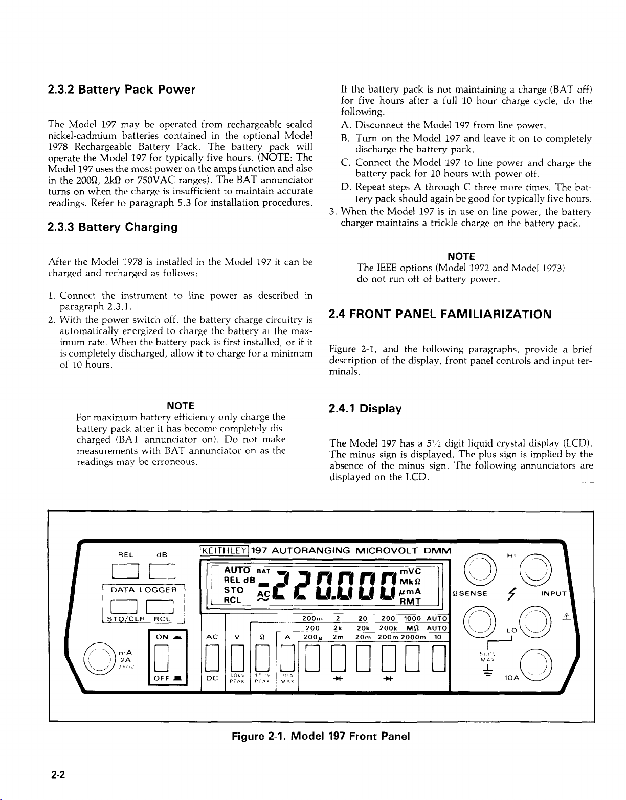
Figure
description of the display, front panel controls and input terminals.
2.4.1
The Model 197 has a
The minus sign is displayed. The plus sign is implied by the
absence of the minus sign. The following annunciators are
displayed on the
2-1,
Display
MICROVOLT
PANEL FAMILIARIZATION
and the following paragraphs, provide a brief
5%
digit liquid crystal display (LCD).
LCD.
DMM
~
I
I
2-2
w
200m
*
QSENSE
u
I
Page 14

BAT-Low battery indicator for the Model 1978.
AC-AC selected (DC implied by the absence of the AC annunciator).
AC/DC-This button is used along with the volts
(A),
rent
AC, releasing (out) this button selects
condition. See Table 2-1.
and dB functions. Depressing (in) this button selects
DC.
AC
!2
(V),
cur-
is invalid
or
mV
O,
p,
RMT
IEEE-488 bus (Model 1973
C-Model 197 in calibration mode.
AUTO-Autorange.
REL-Relative.
dB-Decibel measurement mode.
STO-Data being stored.
RCL-Data being recalled. RCL flashes when buffer is full
during logging cycle.
V-Millivolts or volts.
kO or MO-Ohms, kilohms
mA or A-Microamps, milliamps
(REMOTE)-Model 197 being controlled over the
or
megohms.
or
amps.
or
Model 1972 installed).
2.4.2 Front Panel Controls
ON/OFF-Pressing this button turns on the Model 197.
Releasing (out) this button turns the instrument off.
REL-(RELATIVE)-This button allows readings to be made
of
with respect to any baseline value. Also allows zeroing
range readings. See paragraph 2.7.2 for more detailed infor-
mation on
dB-This button selects the dB function and is used along
with the ACV or DCV function. Measurements are made in
dBm referenced to
voltage level the OdB reference point for dB measurements.
DATA LOGGER and MIN/MAX-100 reading storage
capacity; records data at one
reading/second
(r=6).
readings continuously while in the data logger mode.
REL.
600O.
REL
can be used to make any
of
seven selectable rates from
to
1
reading/hour
Also detects and stores maximum and minimum
or
by manual trigger
on
V-Depressing this button selects the volts function.
0-Depressing this button selects the ohms function. The
AC/DC button must be released (out).
A-Depressing (in) this button selects the current function.
Up to 2A on red and black input jacks and up to 10A with the
black and white input jacks. Refer to paragraph 2.4.3.
RANGE BUTTONS
1.
Depressing AUTO button allows volts and ohms to
autorange. In current,
autorange function for current.
2.
Manual ranging
propriate range button.
it
selects the 10A range. There is no
is
accomplished by depressing the ap-
2.4.3 Input Terminals
The input terminals are intended to be used with safety
shrouded test leads to help minimize the possibility
with live circuits. Safety shrouded tests leads (Model
are supplied with the Model 197. Always disconnect all un-
from
used test leads
HI
and
LO
INPUT (Red and Black)-Use this pair of ter-
minals
1OA
measuring current up to 10A (up to 20A
OHMS Sense HI and LO-Use this pair of terminals along
with HI and
3
for
all volt, ohm, milliamp and dB measurements.
and
LO
(White and Black)-Use this pair of terminals for
LO
the instrument.
for
15 seconds).
input for four wire resistance measurements.
2.4.4 Current Fuse Replacement
of
contact
1751)
1.
STO/CLR-Pressing this button initiates the logging se-
a
quence. Pressing this button
data logger. For
reading is desired, press the STO/CLR button.
2. RCL-Pressing and holding in this button scrolls the data
pointer. To read the data at a certain point, simply release
the button. The logged readings are stored in buffer locations
01
to 102. They are depicted on the front panel as
follows: Buffer location
r=6
rate (manual trigger) every time a
#1
second time turns off the
is represented
___
by n=01.
-
-
Tne current fuse protects the 200pA through 2000mA ranges
from an input current greater than 2A. To replace the current
fuse, perform the following steps:
NOTE
The front panel current fuse (F101) is rated at
2A. With a 220,000 count display, the 2A range
Page 15
can momentarily (approx. one minute) read
2.2A before the fuse will blow. This
range will not harm the instrument.
1.
Turn off the power and disconnect the power line and test
leads.
2. Place the end of a flat-blade screwdriver into the slot in the
fuse holder on the front panel. Press in slightly and rotate
the fuse carrier one quarter turn counterclockwise. Release
pressure and remove the fuse carrier and the fuse.
3. Remove the defective fuse and replace
type: 2A, 250v, 3AG, normal-blow (Keithley part number
FU-13)
or
equivalent.
10%
over-
it
with the following
of less than 80% up to
humidity 3% per "C up to 50°C.
subjected to extremes of temperature, allow sufficient time for
internal temperature
Typically,
(18°F) out of the specified temperature range.
it
takes one hour to stabilize a unit that is 10°C
35°C.
For ambient above 35°C derate
If
the instrument has been
to
reach environmental conditions.
2.6.2 Maximum Allowable Inputs
Table 2-2 lists the maximum allowable inputs for the Model
197.
CAUTION
Use only the recommended fuse type. If a
fuse with a higher current rating is installed, instrument damage may occur.
2.5
ERROR MESSAGES
Table 2-1 lists the error messages associated with basic front
panel operation. Note that the instrument has
other messages that are discussed in the appropirate sections
of the manual.
a
number of
2.6 OPERATING CONDlTlONS
2.6.1 Environmental Conditions
All
measurements should be made at an ambient temperature
within the range of 0°C to 50°C, and with a relative humidity
Table
2-1.
2.6.3 Warm Up
The Model 197 requires one hour for warm
rated accuracy.
up
2.7 BASIC BENCH MEASUREMENTS
Basic measurement techniques for using the Model 197 to
measure AC and DC volts, resistance,
and
dB
are covered in the following paragraphs.
ed is the operation of the minimum/maximum and
data logger.
WARNING
Before operating the Model
previously mentioned safety precautions.
When testing high energy power circuits
follow the instructions found in paragraph
2.2.
Failure to observe these and other safe-
Error
Messages
AC
197,
observe all
and
Also
to achieve
DC
current
includ-
100
point
2-4
3isplay
LC
Err
--
~
Message
I
~
Q11(
Invalid D Function
Comments
Model 197 locks up. See Section 5 for troubleshooting information.
Model 197 locks up, but operation can be restored by pressing
any one of the four momentary pushbuttons. If restored,
calibration is invalid as indicated by the flashing "C" annunciator.
See Section
Overrange input applied to the Model 197. Leading minus sign
indicates that input signal has a negative value.
"AC" and
(out) AC/DC Dushbutton.
5
for troubleshooting information.
"Q"
annunciators flash. Correct problem by releasing
2-3
Page 16
Table
2-2.
Model
197
Maximum Allowable Inputs
-7
Function
DCV
ACV
DCA, ACA
Q
ty precautions mentioned in this manual
could result in severe injury or death.
The
LO
terminal on the Model 197 is designed to float above
earth ground to avoid ground loop problems.
WARN I NG
Hazardous voltage may be applied to the
LO
terminal. The maximum allowable voltage between the
ground is
which could present a shock hazard, may
occur
Do not exceed the maximum input limits
shown in Table
2.7.1
Power
The software revision level of the Model 197 can
be displayed upon power up by running the
diagnostic program. See Section
ance, for more information.
Turn on the Model 197 by pressing in the
All
zeroes are briefly displayed before going into the measure-
ment mode.
If
the Model 197 does not enter the measurement
mode, refer
if
the
Up
500V.
500V
to
LO
Destruction
maximum is exceeded.
CAUTION
2-2.
NOTE
NOTE
section 5.7.1.
Ranges
200mV, 2V
20-1OOOV 1000VDC or peak AC.
i
~OO~V,
'
20-75OV
~
200p-2000mA
I
1 OA
1
terminal and chassis
All
of
5,
1
'
~
2v
insulation,
Mainten-
ON/OFF
Maximum Allowable Inputs
1000VDC or peak AC for less than 10sec per minute.
300~rms continuous.
750Vrms, 1OOOV peak for less than 10sec per
minute.
300Vrms, continuous. lO7*Hz maximum.
750Vrms, IOOOV peak. l07.H~ maximum.
2A, 250VDC or
10A continuous; 20A for 15sec (unfused).
450V peak AC
350Vrms continuous.
switch.
rrns
(fuse protected).
or
DC,
10
seconds per minute,
2.7.2
3.
Relative
When the relative mode is selected with an on-scale reading
on the display the following occurs:
1.
The REL annunciator is displayed.
2.
The next reading is stored.
This reading is algebraically subtracted from all subse-
quent readings and displayed.
A
REL level can be established for any measurement function
(Volts, Ohms, Amps and dB) and
function. Changing functions will not affect a
already established. However,
any function) the previous
ple, place the Model 197 in the ohms function and select the
200Q
range. Short the test leads and press the REL button.
Note that the REL annunciator is on. Select DCV and note
that the
REL
that the
REL
back
celled.
It
REL
braically subtracted from all subsequent readings
function.
Once a
that stored level will be the same regardless of what range the
Model 197 is on.
REL level on the 20VDC range,
other DCV ranges.
REL
level established for DCV. Switch back to ohms and note
REL
level of
to
ohms and note that the
is important to remember what the
function establishes a baseline. That baseline
REL
Mode
is
effective only on that
if
another
REL
level is cancelled.
annunciator is off, indicating that there is not a
level is still there. Again,
+lV.
The REL annunciator turns on. Switch
REL
level for ohms
REL
level is established for a measurement function,
For
example,
if
+1V is established as the
+
1V
is
I
1
I
REL
REL
level is set (on
For
exam-
go
to
DCV and set
is
function does. The
is
for
also the REL level
level
a
can-
alge-
that
for
2-5
Page 17
The dynamic range
means that
applying +1.99999V to the input displays +3.99999V.
Once the REL level is established, that level is algebraically
subtracted from the input signal.
+
1
.OOOOOV
f2.OOOOOV level displays a
if
of
the display is
a
REL
level of -2.OOOOOV is established, then
REL level is established, then applying a
+1.OOOOOV
-+400,000
For
example:
level.
counts. This
if
a
7
The instrument accepts a +220,000 count input before going
(OL).
into the overrange condition
REL
level is established and 1.50000V is applied. The instrument displays +2.500000V. If the input is 2.20000V the instrument overranges.
2.7.3
The Model 197 can make DC voltage measurements between
DC
Voltage Measurement
1pV and
1.
2. Select the DCV function.
3. Select a range consistent with the expected voltage. For
IOOOV.
Connect the test leads to the
of the Model 197.
automatic range selection, press in the
To prolong instrument life, manual ranging is
recommended for routine measurements above
200v.
The basic procedure is as follows:
NOTE
For example:
HI
and
LO
AUTO
-1.OOOOOV
INPUT
button.
terminals
CAUTION.
o/
I
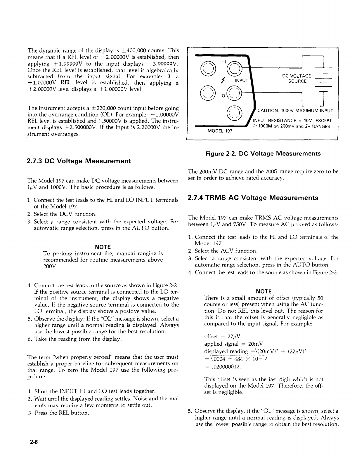
The 200mV DC range and the 2000 range require zero to be
set in order to achieve rated accuracy.
2.7.4
The Model
between
1.
2. Select the ACV function.
3.
4.
MODEL
Figure
TRMS
Connect the test leads
Model 197.
Select a range consistent with the expected voltage.
automatic range selection, press in the AUTO button.
Connect the test leads to the source as shown in Figure 2-3.
197
2-2.
AC
197
can make TRMS AC voltage measurements
1pV
and 750V. To measure AC proceed as follows:
INPUT RESISTANCE = 10M. EXCEPT
>
lOOOM
DC
Voltage Measurements
Voltage Measurements
to
the
HI
on
1OOOV
MAXIMUM INPUT
200mV
and
LO
and
2V
terminals
RANGES
of
the
For
4.
Connect the test leads to the source as shown in Figure 2-2.
If
the positive source terminal is connected to the
minal of the instrument, the display shows a negative
If
value.
LO
5. Observe the display;
higher range until a normal reading is displayed. Always
use the lowest possible range for the best resolution.
6.
Take the reading from the display.
The term "when properly zeroed" means that the user must
establish a proper baseline for subsequent measurements on
that range. To zero the Model 197 use the following pro-
cedure:
1.
Short the INPUT
2. Wait until the displayed reading settles. Noise and thermal
emfs may require a few moments
3. Press the
2-6
the negative source terminal is connected to the
terminal, the display shows a positive value.
If
the
"OL"
message is shown, select a
HI
and
LO
test leads together.
to
settle out.
REL
button.
LO
ter-
NOTE
There is a small amount of offset (typically 50
counts
tion.
this is that the offset is generally negligible as
compared to the input signal.
offset
applied signal
displayed reading =\(20mV)2
This offset is seen as the last digit which is not
displayed on the Model 197. Therefore, the offset is negligible.
5.
Observe the display,
higher range until a normal reading is displayed. Always
use the lowest possible range to obtain the best resolution.
or
less) present when using the
Do
not REL this level out. The reason for
=
22pV
=m-+484
=
.0200000121
=
20mV
x
10-iZ
if
the
AC
For
example:
+
(22pV)Z
"OL"
message is shown, select a
func-
Page 18

6. Take the reading from the display
NOTE
See paragraph
When measuring
leads from the OHMS SENSE terminals.
-INPUT
MODEL
197
2.8
for TRMS considerations.
AC
signals disconnect any test
IMPEDANCE
BY
<
75pF
=
IMR
SHUNTED
R,
=
parallel combination of source resistance and input impedance.
e, = Johnson noise of the source resistance.
on
Even
is
Thus, for an R, of
inherent 1.5pV peak to peak. Beyond
to R, becomes a limiting factor in the measurement.
Therefore, it is recommended that
ments R, be kept relatively 10~7,
As
(due to Johnson noise of the source resistance) assume that the
Model 197 is connected to a voltage source with an internal
resistance of
p-p noise voltage generated over a bandwidth
most sensitive range, the noise due to the current
not appreciable until R, reaches approximately
OQ
to
lMQ,
the noise at the input is the
1MQ
the noise due
for
sensitive measure-
if
possible below
an example of determining e, noise voltage generation
1MQ.
At
a
=
e,
e, = 6.35
room temperature
6.35
X
10-10
X
lO-lO\r(lx
\J
R
X
10m
of
20°C
of
f
1MQ.
(293K),
1Hz
will be:
lMQ.
the
Figure
2.7.5
Accuracy Considerations-For sensitive measurements, other
external considerations besides the Model
accuracy. Effects not noticeable when working with higher
voltages are significant in microvolt signals. The Model 197
reads only the signal received at its input; therefore,
portant that this signal be properly transmitted from the
source. The following paragraphs indicate factors which af-
fect accuracy, noise, source resistance, thermal emfs and
stray pick-up.
Noise and Source Resistance-The limit of resolution in
measuring voltages with the Model 197 is determined by the
noise present. The displayed noise of the Model 197 is 1.5pV
peak to peak. This noise is inherent in the Model 197 and is
the minimum amount present in all measurements. The 1.5pV
of noise is due to the instrument voltage noise. The noise at
the Model 197 input increases beyond this minimum when the
noise current passes through a resistor thus generating a
voltage noise. The total noise becomes a function of the
source resistance and is given by the equation:
2-3.
TRMS
AC
Voltage Measurements
Microvolt Measurement Considerations
197
will affect the
it
is im-
=
en2
+
n2
(inRs)2
+
er2
e, = 0.635pV
Thus
it
is clear that optimum microvolt measurements with
the Model 197 are possible with source resistances as high as
1MQ.
However, this resolution will not be realized unless
shielding is employed.
Shielding-The Model 197 is insensitive
DC
superimposed upon a
However,
with the
Therefore,
shielded and the shield connected to the Model 197 ground
(particularly for low-level sources). Improper shielding can
cause the Model 197 to behave in one
ing ways:
1. Unexpected offset voltages.
2.
Inconsistent readings between ranges.
3.
Sudden shifts in reading.
To minimize pick up, keep the voltage source and the Model
197 away from strong
duced due to magnetic flux is proportional to the area
loop formed by the input leads. Therefore, minimize the loop
area of the input leads and connect each signal at only one
point.
AC
voltages which are extremely large compared
DC
signal may erroneously produce
if
there is
AC
signal at the input terminals.
interference, the circuit should be
AC
magnetic sources. The voltage in-
to
AC
voltages
a
DC
output.
or
more of the follow-
of
the
where
n
=
total noise input.
=
input voltage noise of the Model 197.
en
in
=
input current noise.
Thermal EMFs-Thermal emfs (thermoelectric potentials) are
generated by thermal differences between two junction
dissimilar metals. These can be large compared
which the Model 197 can measure. Thermal emfs can cause
the following problems:
to
the signal
of
2-7
Page 19
1.
Instability
2. The reading is sensitive to (and responds to) temperature
changes. This can be demonstrated by touching the circuit,
by placing a heat source near the circuit
pattern of instability (corresponding to heating and airconditioning systems or changes in sunlight).
3. To minimize the drift caused by thermal emfs, use copper
leads to connect the circuit to the Model 197.
plug is generally sufficient and generates just a few
microvolts.
is about the best for the application. The leads to the input
may be shielded
Shielding.
4.
Widely varying temperatures within the circuit can also
create thermal emfs. Therefore, maintain constant temperatures to minimize these thermal emfs.
box around the circuit under test also helps by minimizing
air currents.
5. The REL control can be used to null out constant offset
voltages.
2.7.6
The Model 197 can make resistance measurements between
1m3 and 22OM3. The 2M3, 20MQ and 200MQ ranges
autorange when the
provides automatic selection of 2-terminal
resistance measurements. This means that
leads are not connected, the measurement is done &terminal.
If
the sense leads are connected the measurement is done
4-terminal. For 4-terminal measurements, rated accuracy can
be obtained as long as the maximum lead resistance does not
exceed the values listed in Table 2-3. For 2-terminal
4-terminal measurements on the 2003 range, zero must be set
by the REL function to obtain rated accuracy. For best results
on the 2003, 2k3 and 2Ok3 ranges, it is recommended that
4-terminal measurements be made to eliminate errors caused
by the voltage drop across the test leads that occurs when
2-terminal measurements are made. To make resistance
measurements, proceed as follows:
or
zero offset is much higher than expected.
A
clean copper conductor such as
or
unshielded, as necessary. Refer to
Resistance Measurements
M3
button is selected. The Model 197
or
by a regular
A
banana
#lo
bus wire
A
cardboard
or
4-terminal
if
the ohms sense
or
1.
Connect the test leads to the HI and
If four-wire measurements are to be made, connect an additional set of leads to the OHMS SENSE terminals.
NOTE
The Model 1641 Kelvin test lead kit is ideal for
low resistance 4-terminal measurements.
2. Select the ohms function.
3.
Select a range consistent with the expected resistance.
desired, use the autorange mode for automatic range selection.
4.
If
readings are to be made on the 2OOQ range, zero the instrument to obtain rated accuracy. To zero the instrument
for resistance measurements: Short the test leads together
after disconnecting them from the measured circuit:
4-wire measurements are to be made, short
leads as shown in Figure 2-6, allow the reading to settle
REL
then press the
5.
For 2-wire measurements connect the instrument as shown
in Figure 2-4. For 4-wire measurements, use the connections shown in Figure 2-5.
The maximum input voltage between the
HI
and LO INPUT terminals is
peak AC for
RMS
values or instrument damage may occur.
Table
various resistance ranges.
Incorrect readings will result if the
resistance being measured is part
circuit.
6. Take the reading from the display.
continuous. Do not exceed these
2-3
button.
CAUTION
10
seconds per minute,
shows the current output for
CAUTION
LO
450V
INPUT
all
DC or
350V
of
a live
terminals.
four test
If
if
2-8
Range
200
2k
20 k
,
200 k
200M
tesolutior
lm3
1
OmQ
1
OOmQ
1Q
10
0
100
Q
10
k3
Table
I-S
hort
2mA
2mA
400pA
40 pA
4 PA
400 nA
400 nA
2-3.
Resistance Ranges
Across
Unknown
4.0V
4.0V
5.0V
Maximum Test Lead
Resistance for
(1
Count Error
10
(Q)
32
100
320
Ik
3.2k
10k
Page 20
NOTE
It
is helpful to shield resistance greater than 106Q
(1MQ)
resistance in a shielded enclosure and electrically
connect the shield to the
the Model 197.
-
if
a stable reading is expected. Place the
LO
input terminal of
OPTIONAL SHIELD
__
RESISTANCE
2.7.7
Current Measurements
(DC
or TRMS
AC)
The Model 197 can make DC or TRMS AC current
measurements between 1nA and 10A (20A for
the expected current level is in question, make the initial
measurement on the 10A range. This helps prevent inadvertent blowing of the 2A current fuse which is located on the
front panel.
I
I
NOTE
For routine measurements above 10A
recommended that the Model 1651 50A shunt be
used.
15
seconds).
it
If
is
Figure
MODEL 197
2-4.
Two
MODEL 197
Figure
CAUTION: MAX INPUT
or PEAK AC for lOsec/min, 350V
[
RMS CONTINUOUS
=
450VDC
Terminal Resistance Measurement
OPTIONAL SHIELD
I-----
CAUTION: MAX INPUT = 450VDC
or
pk
AC for 10sec/min, 350V RMS
CONTINUOUS.
2-5.
Four Terminal Resistance
-
-
---
Measurement
1.
For current measurements between 2000mA and 20A.
to
A. Connect the test leads
the Model 197. Refer
The test leads used must be rated to handle 20A.
Twist the wires as shown in Figure 2-7
minimizing external fields which could affect the
I
I
Model 197 or other equipment. Also, keep the
test leads as short as possible
voltage drop.
B.
Select the ACA or DCA function.
C. Select the 10A range. The amps function does not
autorange.
D. Connect the test leads to the current source as shown in
Figure 2-7 and take the reading from the display.
Up to
5A
may be applied continuously without
degradation of the measurement due to self
heating effects. Above
amp for self heating, refer to specifications that
precede Section
20A, specified accuracy can only be obtained
when measurements are limited to a maximum
of
15
seconds.
1.
the 10A and
to
Figure 2-7.
NOTE
NOTE
5A
derate
For
currents between 10A and
to
0.15%
LO
terminals
to
help in
minimize
rdg per
of
INPUT
LO
OHMS SENSE LO
OHMS SENSE HI SHORT
Figure 2-6. Four Terminal Zeroing
2.
For
current measurements up to 2000mA:
A.
Connect the test leads to the INPUT
minals
B.
Select the ACA or DCA function.
C.
Select an appropriate range for the expected current.
The current function does not autorange.
of
the Model 197.
HI
and
LO
ter-
2-9
Page 21

D.
Connect the test leads to the current source as shown in
Figure 2-8.
select a higher range until a normal reading
Use the lowest possible range to obtain the best resolution.
E.
Take the reading from the display.
If
an overrange indication is displayed,
is
shown.
1.
Measure and record the
cribed in paragraph 2.7.4.
2. Measure and record the
paragraph 2.7.3.
3. Compute the rms value from the following equation:
Em,
TRMS
DC
component as described in
=UE~D~
+
AC component as des-
E~AC
-CAUTION:
MODEL
197
MAX INPUT
=
IOA
Figure 2-7. Current Measurements Between
2000mA and 20A
2.7.9
dB
Measurements
The dB function makes
of
readings into a much smaller scope. The relationship bet-
ween dB and voltage can be expressed by the following equa-
tion.
it
possible to compress a large range
VIN
dB
=
20
log-
VREF
Tables 2-4 and 2-5 list the
AC volts.
The Model 197 can make
600Q
standard
relative feature allows measurements in
impedance.
The basic procedure
mode is
button. Note that once
pressing in the
to
impedance
first select AC or DC volts and then press the
Q
or A function pushbuttons will turn
dB
specifications for DC volts and
dB
measurements referenced to the
or
to other impedances. The
dB
independent
for
placing the instrument in the dB
dB
is selected
(dB
annunciator on),
dB
dB
off.
of
Figure
2.7.8 AC
Use the Model 197 to measure TRMS on a signal which has
both AC and
2-10
2-8.
Current Measurements up to 2000mA
Plus
DC
Measurements
DC
components.
Table 2-4. dB Specifications for DC Volts
(600Q
Linear
~ Counts
10-99
100-999
1000-9999
10000-220,OOO
Ref)
Resolution Accuracy
IdBrn
0.ldBrn
0.OldBrn +O.ldBrn
0.01 d
Brn
k
2dBrn
k
-t
0.02dBrn
IdBrn
typical
Page 22

Table
dB
Range
200mV
2-5.
M
dB
de (Ref:
InDut
1mV
(-58
to
2mV
(-52
to
20mV
(-32
to
Specifications for
60001
20Hz-
10kHz
to
2mV
-52dBm)
to
20mV
-32dBm)
to
200mV
-12dBm)
2.00
0.85
0.18
AC
Volts
Accuraci
10kHz-
2OkHz
3.00
1.10
0.18
(600n
(
k
dBw
ZOkHz-
50kHz
-
2.00
0.28
Ref)
5OkHz100kHz
-
-
0.65
ZV-75OV
dBm
Measurements with
dBm is defined as decibels above
The standard reference impedance of the Model 197 is 6000.
What that means is that the Model 197 is designed to read
OdBm when the voltage needed to dissipate 1mW through a
600a
impedance is applied to the Model 197. That calculated
voltage level is 0.7746V as derived from the basic power
equation.
~~
E=h’.R
E
=q0--3
E
=
0.77456V
Thus with a 6000 reference impedance the Model 197 will
read OdBm whenever 0.7746v is applied.
Do
not confuse reference impedance with input
impedance. The input impedance
ment is not modified in the dB mode.
To
make dBm measurements referenced
follows:
-
W.6000
600a
Reference Impedance
NOTE
200mV
1-12
or
below a 1mW reference.
of
to
to
750V
to
+59.8dBm)
the instru-
6000, proceed as
0.18
dBm Measurements with Other Reference Impedances
dBm measurements can be made with other reference impedances. The most convenient method for using other
reference impedances is to algebraically subtract the
calculated dB offset for the desired reference impedance from
the reading on the display of the Model 197. Table 2-6 lists
common reference impedances and the corresponding offset
values. The following equation can be used to calculate the
offset the offset for impedances not listed in Table 2-6.
To
pedance, proceed as follows:
1.
2. Calculate
3.
0.18
make dBm measurements referenced to another im-
Choose the desired reference impedance.
desired reference impedance.
Determine dBm at the desired reference impedance as
follows:
Example: Make dBm measurements references to a 1000
reference impedance.
0.28
Offset (for dBm) = 10 log----
or
look up the offset value in Table 2-6 for the
dBm (at ref
0.50
Z)
=
197 reading - offset
New ref
600Q
Z
1.
Connect the test leads to the INPUT
of the Model 197.
2. Select the ACV
3.
Select autorange for optimum resolution.
4.
Press the dB button.
5.
Connect the test leads to the voltage source.
6. Make the dBm reading from the display.
or
DCV function.
HI
and
LO
terminals
A.
1000 not listed in Table 2-6
calculated as follows:
Offset
B.
Subtract -7.78 from all subsequent displayed readings
on the Model 197.
=
10 log
Offset = -7.78dB
so
the offset must be
(z
)
2-1 1
Page 23

dBm measurements, referenced to another impedance, can be
read directly from the display of the Model 197 by utilizing
the
REL
feature, and an accurate voltage source. The basic
procedure is as follows:
1.
Calculate
2-6) for OdBm at the desired reference impedance.
2. Input that voltage level to the Model 197.
3. With the Model 197 in the
4.
dBm measurements referenced to the desired impedance
can now be read directly from the display
197.
dBW
dBW is defined as decibels above
reference. The procedure
paragraph 2.7.9 step 2.
reference point is OdBW (1W) rather than OdBm (1mW).
dBV
Measurements
dBV is defined as decibels above or below 1V (OdBV point).
This is a voltage relationship independent of impedance. The
basic procedure is to simply subtract 2.22 dB (Table 2-6) from
all subsequent displayed readings on the Model 197.
Relative
Just about any voltage level within the measurement limit of
the Model 197 can be established as the OdB point. The basic
procedure is to establish the level as the OdB point by using
REL and make the desired dB measurements.
2.7.10
or
look up the equivalent voltage level (Table
dB
Measurements
dB
Measurements
mode, press the
or
is
the same as that found in
The only difference is that the
REL
of
the Model
below a one watt
dB Measurement Considerations and
button.
Applications
1.
Typical Instrument Performance
Typically, the Model 197 will perform better that its
published dB specification. The following example will
lustrate this point:
A.
Using the Model 197 in the dB mode (6003 ref) measure
a ImV
communications field). Typically, the Model 197 will
read -57.7dBm.
The calculated dBm level for that source is -57.8dBm.
B.
The O.1dBm error is considerably better than the
C.
+
to cover worst measurement conditions.
RMS,
1kHz source (common application in the
2dBm specification. The specifications are intended
il-
Table
2-6.
Levels for Other Reference Impedances
I
Reference 1 Reference Voltage
'
Impedance
I
~
~
Offset
Vref
Vref,
(Q2)
150
300
for
for
(for
8
50
75
OdBm
OdBW
dBm) = 10
Level for:
OdBm OdBW
0.0894 2.828
0.2236
0.2739
0.3873
0.5477
0.7746
1
.oooo
=
\
ZREF
~
log
I
'
.
Offset
(600Q
Ref)
OdBm OdBW
-
18.75 11.25
-
10.79
-
9.03
-
6.02
-
3.01
0.00
I
2.22
Cblb:!)
Offset
2. Measuring Circuit Gain/Loss
3. Measuring Bandwidth
(for
dBW) = 10
Any point in a circuit can be established as the OdB point.
Measurements in that circuit are then referenced to that
point expressed in terms of gain (+dB) or
set the OdB point:
A. Place the Model 197 in volts, autorange and dB.
B.
Connect the Model 197 to the desired location
circuit.
C. Press the
D. Gain/Loss measurements can now be made referenced
to the OdB point.
The Model 197 can be used to determine the bandwidth of
amplifier as follows:
an
Connect a signal generator to the input of the amplifier.
A.
Set the Model 197 to ACV and autorange.
B.
Connect the DMM and a frequency counter to the load
C.
of the amplifier.
Adjust the frequency of the signal generator until a
D.
peak AC voltage reading is measured on the Model
197.
Press the dB button and then press the
E.
OdB point
Increase the frequency input until the Model 197 reads
F.
-
3.00dB. The frequency measured on the frequency
counter is the high end limit of the bandwidth.
Decrease the frequency input until the dB reading again
G.
falls to -3dB. The frequency measured on the signal
generator is the low end limit of the bandwidth.
REL
is
log
(zR:ooQ
button. The display will read OdB.
now established.
)
REL
-30dB
loss
(-dB). To
button. The
in
the
I
I
2-12
Page 24

4.
Determining
The Q of a tuned circuit can be determined as follows:
A. Determine the center frequency and bandwidth as ex-
plained in paragraph 2.7.10 step
B.
Calculate Q by using the following formuala:
Q
Q
=
Center Frequency/Bandwidth
3.
The logging cycle can be terminated at any time
by pressing the STO/CLR button. This shuts off
the data logger. However, data is retained and
can be recalled at any time as long as the instrument remains on. In the
RCL and the STO/CLR button to terminate the
data logger cycle.
2.7.11 MIN/MAX and 100 Point Data Logger
Operation
The data logger can store up to
minimum and maximum readings recorded during the period
that the data logger is active. The
stored at one of seven selectable rates from three per second
to one reading per hour. Also, manual triggering is available
(r=6). In the r=6 mode, one reading is stored every time the
STO/CLR button is pressed. Readings for minimum and
maximum are sampled at the rate of three per second
regardless of the selected rate. The procedure for operating
the data logger is as follows:
Connect the desired measurement configuration to the
1.
Model 197. Make sure that the controls of the Model 197
are set appropriately. the display.
Logging Data:
2.
A. Press and hold the STO/CLR button. The following
reading rates will scroll on the display:
rate/ meaning
r
=
0
(every reading)
r=l
(1
rdg/sec)
r=2
(1
rdg/lo sec)
r=3
(1
rdg/min)
r=4
(1
rdg/lo min)
r=5
(1
rdg/hour)
r=6 (Irdg every time STO/CLR is pressed)
There is no need to select a rate
minimum/maximum readings are desired. Press
the STO/CLR button to start the logger.
NOTE
100
readings and store the
100
points of data are
if
just
In the store mode
is full
readings are continuously updated. When the store mode
turned off the minimum and maximum readings are not updated.
3.
(100
Data Retrieval-Data can be retrieved at any time, but a
flashing
number of readings
A. Press and hold in the RCL button. The display scrolls
through the data points and MIN/MAX (LO/HI). The
first data point displayed is the last stored reading. The
next two data Doints are the
during that logging cycle. Notice that the longer the
RCL
B.
Release the
note the reading (data) on the display. The data pointer
can be incremented by steps of one by momentarily
holding in the RCL button.
2.7.12 Diode Test
The 2kQ and 2OOkQ ranges can be used for testing semiconductor junctions as follows:
1.
Select the ohms function.
2.
Press the 2k and 2OOk button (diode symbols) in
simultaneously.
3.
Display reads forward V drop of a silicon diode at 1.6mA
(l.lmA for an LED), up to 2.2V. Red terminal is positive.
Accuracy is typically better than
NOTE
r=6
mode, press the
(STO
annunciator on) and when the buffer
readings stored), the minimum and maximum
is
RCL
annunciator indicates that the maximum
(100)
have been stored.
HI
and
LO
readinas made
<I
button is held in the faster the data points scroll on
RCL
button at the desired data point and
1.5%
of reading.
B.
Release the STO/CLR button when the desired reading
rate is displayed. The STO annunciator turns on and
data is logged at the selected rate.
C. In the manual trigger mode (r=6), a reading is stored
every time the STO/CLR button is pressed. The follow-
ing sequence takes place after the STO/CLR button is
pressed when in the manual trigger mode.
a. The Model
b. The buffer location number is briefly displayed. For
example: Buffer location
c. The Model 197 displays the applied signal and waits
for the next manual trigger.
197
stores the reading.
#1
is represented by n=01.
2.8 TRMS CONSIDERATIONS
Most DMMs actually measure the average value of an input
waveform but are calibrated to read its
poses no problems as long as the waveform being measured is
a pure, low distortion sine wave. For complex, nonsinusodial
waveforms, however, measurements made with an averaging
type meter can be grossly inaccurate. Because
(True Root Mean Square) measuring capabilities, the Model
197 provides accurate AC measurement for a wide variety of
AC input waveforms.
RMS
equivalent. This
of
its TRMS
2-13
Page 25

2.8.1
AC
Voltage Offset
Typically, the Model
on
AC
volts with the input shorted. This offset is caused by
amplifier noise and offset of the TRMS converter. This offset
does not affect the reading accuracy and should not be zeroed
out using the
REL
197
displays
feature. Refer to Paragraph
50
counts
or
less of offset
2.7.4
step
4.
2.8.2 TRMS Measurement Comparison
The situation changes with
wave.
As
before, the peak value of the waveform is
the average value drops to
waveform is
3.53V
A
similar situation exists
which has
Here,
(5
x
l.ll),
Other waveform comparisons can
5v,
but the average responding meter will @ve
(3.18
x
1.11>,
creating an error
an
average value of
the average responding meter gives a reading of
while the Model
the
half-wave rectified sine
3.18V.
The
of
for
the rectified square wave,
5V
and an
197
gives a
be
TRMS
found
RMS
29.4%.
RMS
lOV,
value
value
reading
in
Table
but
of
this
of
5V.
5.55V
of
5V.
2-7.
The RMS value of a pure sine wave is equal to
peak value. The average value of such a waveform is
times the peak value. Thus, for an average-responding meter,
a correction factor must be designed in. This correction fac-
tor,
K,
can
be found by dividing the
average value as follows:
0.707
K
=--
BY
applying this correction factor to an averaged reading, a
typical meter can be designed to give the
This works fine as long as the waveform is a Pure sine wave,
but the ratios between the RMS and average values of dif-
ferent waveforms is far from constant, and can vary con-
siderably.
Table
waveforms. For reference, the first waveform is an ordinary
sine wave with a peak amplitude of
of
be seen that both meters will give the same reading, resulting
in no error in the average type meter reading.
2-7
shows a comparison of common types of
this voltage is
the
l.il
correction
6.37V,
while its RMS value
factor
0.637
-
1.11
1OV.
to
the
average reading,
0.707
times its
0.637
RMS
value
by the
RMs
equivalent.
The average value
is
7.07V.
If we
it
can
2.8.3 Crest Factor
The crest factor
its RMS value. Thus, the crest factor specifies the dynamic
range of a TRMS instrument. For sinusodial waveforms, the
crest factor is
factor is unity.
The crest factor of other waveforms will,
on the waveform in question because the ratio of peak
RMS value varies.
tangular pulse is related to its duty cycle; as the duty cycle
decreases, the crest factor increases. The Model
crest factor of
TRMS measurements of rectangular waveforms with duty
cycles as low as
of
a waveform
1.414.
For a symmetrical square wave, the crest
For
3,
which means the instrument gives accurate
10%.
is
the ratio
example, the crest factor
of
its peak value to
of
course, depend
197
of
a rec-
has
2.8.4 Extended F~~~~~~~~ Response
Figure
ACV
2-9
illustrates the extended
ranges
up
to
lMHz.
frequency response
of
the
to
a
2-14
Page 26

-
E
1M
loot
10K
w
1
A
I
4
1K
100
10
t
I
t
t
~
+--
-i
-1
I
L
0
N
0
0
U
w
U
B
0
0
m
0
c
in
Page 27

Waveform
Table
2-7.
Comparison of Average and TRMS Meter Readings
Ac Coupled
Ac Coupled
Peak
Value
RMS
Value
Average
Responding
Meter Reading
TRMS
Meter
Reading
Averaging
Meter
Percent Error
Half-Wave Rectified Sine
Full-Wave Rectified Sine
+
lo-
-
0
-m-
Square
+lo-:%
Rectified Square Wave
+
10-
-
1ov
1
ov
1
ov
1
ov
1
ov
7.07V
5.00V
7.07V
1o.oov
5.00V
7.07V
3.53v
7.07V
11.1ov
5.55v
7.07V
5.00V
7.07V
1o.oov
5.00V
0%
29.4%
0%
11%
1 1
7c
00
Rectangular Pulse
+1°53L
O-N
k-trlT
ll:
'DUTY
CYCLE'
Triangular Sawtooth
2-16
1
1
ov
ov
1ov
5.77v
11.1V.
5.55v
q
1ov
5.77v
1.11
-
1)
3.8%
x
100%
Page 28
3.1 I NTR 0 D U CTI 0 N
SECTION
3
PERFORMANCE VERIFICATION
3.3
RECOMMENDED TEST EQUIPMENT
This section contains information necessary to verify that the
Model
197’s
performance is within specified accuracy. Model
197
specifications may be found at the front of this manual.
Ideally, performance verification should be performed when
the instrument is first received to ensure that no damage
change in calibration has occurred during shipment. The
verification procedure may also be performed whenever in-
or
strument accuracy is suspect
formance on any of the ranges
with specifications, calibration should be performed as
described in Section
If
the instrument does not meet specifications
and
it
months since date of shipment), contact your
Keithley representative
mine the action to be taken.
3.2
E
N
V I R
0 N M
All measurements should be made at an ambient temperature
between
humidity less than
18°C
5.
is still under warranty (less than
E
NTA L C 0 N D IT
and
28°C (65°F
80
%
.
following calibration. If per-
or
functions is inconsistent
NOTE
or
the factory to deter-
I0
N
S
to
82°F)
with a relative
or
12
Equipment for verifying the performance of the Model
listed in Table 3-1. Alternate equipment may be used as long
as equipment accuracy is at least equal to the specifications
listed in Table 3-1.
3.4
INITIAL CONDITIONS
Before performing the verification procedures, make sure the
Model
1.
2.
3.5
The following paragraphs give the basic verification procedure for the following functions
resistance and current
197
meets the following conditions:
If
the instrument has been subjected to temperature below
18°C (65°F)
the instrument to reach temperatures within the range.
Generally,
10°C
is
Turn on the Model
hour. The instrument may be operated from either line
power of battery pack power, as long as the battery pack
has been fully charged as described in paragraph
VERl FICATION PROCED U
or
above
28°C (82”F),
it
takes one hour to stabilize an instrument that
(18°F) outside of this range.
197
and allow
allow sufficient time for
it
to warm up
RE
DC
volts, AC volts,
197
for
2.3.3.
one
is
I
Mfg
Fluke
Fluke
Valhalla
Fluke
Fluke
I
Model I Description
343A
5200A
2500E
5450A
521 5A
DC Voltage Calibrator
AC Voltage Calibrator
AC-DC Current Calibrator
Resistance Calibrator
Power Amplifier
Table
3-1.
Equipment Specifications
I
Specifications
200mV, 2V, 20V, 200V, 1 OOOV ranges
200mV, 2V, 20V, 1 OOV 50Hz
200pA, 2mA, 20mA, 200mA, 2000rnA, 1 OA ranges
50.03% DC,
I
OOR,
1
range
+O.O1°/o;
&0.5%
1
OOOV range: 1 OHz-30Hz
-tO.IO%;
max
@
=.
+0.1%
ka,
1
OkR, 1 OOkn
10MQ
1
OOV max
13kHz
=
f0.005%
to
1 OkHz
+0.05%
AC to 5kHz (at full scale)
ranges
range 50.05°/o;
k0.12%;
@I
1
OOkHz = 10’VHz; 750V
1
07VHz
+0.005%; 1 MR
1
OOMQ
50kHz-l OOkHz
3-1
Page 29

-
.,?
WARNING
The following procedures require that high
voltages may be applied to the input ter-
minals of the Model 197. Use normal safety
precautions to avoid possible electrical
shock which could result in personal injury
or death.
3.5.1
DC
Voltage
1.
Select the
2. Connect the calibrator to the instrument as shown in
Figure
3. Set the calibrator to
Leave the relative mode enabled for all DCV
measurements. Check to see that the reading is 000.OOOV
+1
4.
Apply a positive 200mV to the
minals. The reading must be within the limits specified in
Table 3-2.
5. For each remaining range, apply the required voltage as
specified in Table 3-2 and verify that the reading is within
specifications.
6.
Repeat all checks with negative voltage.
DC
Do not exceed IOOOV between the input HI
and
LO
terminals or damage to the instru-
ment may occur.
3-1.
count.
Accuracy Check
volt function and autorange.
CAUTION
OV
and enable the relative mode.
HI
and
LO
INPUT
ter-
Table 3-2. Limits for DC Voltage Verification
197
DCV Range
200mV
2v
20
v
200
v
1000
v
*The limits shown do not include test equipment
tolerances.
3.5.2
AC
Voltage
Do not exceed 750V RMS, IOOOV peak
107VHz between HI and
minals or instrument damage may occur.
1.
Select the AC volts function and autorange. Do not use
REL
to zero the offset in this procedure. Refer to paragraph
2.7.4 step
2. Connect the AC calibrator to the HI and
minals of the Model 197 as shown in Figure 3-2.
3.
Set the calibrator to output 2.OOOOOV at a frequency of
50Hz. Verify that the reading is within the limits specified
in Table
4.
Repeat the 2.OOOOOV AC measurement at the other frequencies specified in Table 3-3.
5. Check the 2OV, 2OOV and 750V ranges by applying the required voltage and frequencies specified in Table
verifying that the readings are within the specified limits.
3-3.
Applied
DC Voltage
200.000mV
2.00000
20.0000
200.000
1000.00
4.
Allowable Readings*
(18OC to 28OC)
199.965
v
v
v
v
1.99976
19.9968
199.968
999.68
Accuracy Check
CA UTlO N
LO
INPUT ter-
to
200.035
to
2.00024
to
20.0032
to
200.032
to
1000.32
LO
INPUT ter-
3-3
and
I
MODEL 197
Figure 3-1. Connections for DCV Verification
3-2
I
HI
AC
CALIBRATOR
MODEL 5200A
and
10
MODEL 197
MODEL 5215A
Figure 3-2. Connections for ACV Verification
Page 30

Table
3-3.
Limits for
AC
Voltage Verification
197 AC
Range
200rnV
2v
20
200
750 V
3.5.3
Resistance Accuracy Check
Resistance verification is performed by connecting known,
precise resistance values to the
checking to see that the displayed reading is within the required limits. Measurements on the
ranges will be done using the 4-terminal configuration to
minimize errors due to the voltage drop across the test leads.
Do not exceed 450VDC
seconds per minute, 350V rms continuous
between the HI and
the instrument might be damaged.
1.
Select the ohms function (AC/DC button must be out) and
the
2003
range.
2. Use Kelvin test leads (e.g. Keithley Model
put
HI
and
LO,
and then
minals. Short the leads together. Enable the relative (REL)
mode. Check to see that the display reads
the relative mode enabled for the remaining resistance
measurements.
3.
Connect
3-3.
measurement.
4.
Check to see that the displayed reading is within the
limits specified in Table
a
1903
calibration resistor as shown in Figure
Note that the 4-terminal configuration is
Applied
AC Voltage
200.000rnV
2.00000v
20.0000v
v
200.000v
v
7 50. OOOV
HI
CAUTlO
LO
OHMS
3-4.
20Hz
197.900
to
202.100
1.97900
to
2.02100
19.7900
to
20.2100
197.900
to
202.100
739.63
to
760.37
and
LO
input terminals and
2OOQ,
2kQ
and 2Okn
N
or
peak AC
INPUT terminals or
SENSE
for
10
1641)
in the in-
HI
and
000.000.
used
50Hz
199.200
to
200.800
1.99200
to
2.00800
19.9200
to
20.0800
199.200
to
200.800
743.37
to
755.62
LO
ter-
Leave
for this
10kHz
198.600
to
201.400
1.98600
to
2.01400
19.98600
to
20.1400
199.860
to
201.400
740.50
to
759.50
5.
Connect
shown in Figure
range. Verify that the displayed reading is within the
limits specified in Table
6.
Connect a 19kO calibration resistor to the instrument as
shown in Figure 3-3. Switch the instrument to the 20k3
range. Verify that the displayed reading is within the limits
specified in Table 3-4.
7.
Connect a 190kn calibration resistor to the instrument as
shown in Figure 3-4. Switch the instrument to the 200k3
range. Verify that the displayed reading is within the limits
specified in Table 3-4. Note that the 2-terminal configuration may be used on the 2OOkn and higher ranges.
8.
Continue with each of the calibration resistance values
listed in Table 3-4. Be sure to place the Model
correct range for each measurement. The remaining
readings may be done using 2-terminal configuration.
Table
197 Range
;j:
3-4.
200
20M
200M
2OkHz
196.750
to
203.250
1.96750
to
2.03250
19.6750
to
20.3250
196.750
to
203.250
a
1.9kn
50kHz
189.600
to
210.400
1.93600
to
2.06400
19.3600
to
20.6400
193.600
to
206.400
calibration resistor
3-3.
Switch the instrument to the
100kHz
189.600
to
210.400
1.93600
to
2.06400
19.3600
to
20.6400
to
the
3-4.
Limits for Resistance Verification
k
Applied
Resistance
190.000
1.90000
19.0000
190.000
1.9OOOOMfl
19.0000Mn
190.000Mn
kQ
k!J
kQ
Allowable Readings
I
(18OC to 28OC)
n
189.959
1.89964
18.9949
189.949
1.89931
18.9770
186.199
to
to
to
to
to
to
to
instrument
197
on the
190.041
1 .go036
19.0051
190.051
1.90069
19.0230
193.801
as
2kfl
3-3
Page 31
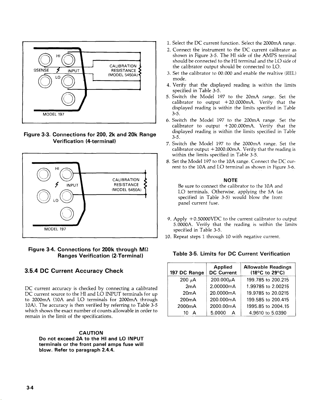
Figure
3-3.
Connections for
Verification (4-ter m i nail
HI
200,2k
1,
and
20k
CALIBRATION
RESISTANCE
(MODEL 5450A)
Range
I
1.
Select the
2. Connect the instrument to the DC current calibrator as
shown in Figure
should be connected to the HI terminal and the
the calibrator output should be connected to
3.
Set the calibrator
mode.
4.
Verify that the displayed reading is within the limits
specified in Table
5.
Switch the Model 197
calibrator to output +20.0000mA. Verify that the
displayed reading is within the limits specified in Table
DC
current function. Select the
3-5.
The HI side of the
to
00.000
and enable the realtive
3-5.
to
the 20mA range. Set the
20OOmA
AMPS
LO
LO.
range.
terminal
side of
(REL)
3-5.
6.
Switch the Model 197 to the 200mA range. Set the
calibrator to output +200.000mA. Verify that the
displayed reading is within the limits specified in Table
3-5.
7.
Switch the Model 197 to the 2000mA range. Set the
calibrator output
within the limits specified in Table
8.
Set the Model 197
rent to the 10A and
Be sure to connect the calibrator
LO
terminals. Otherwise, applying the
specified in Table
panel current fuse.
+
2000.00mA. Verify that the reading is
3-5.
to
the 10A range. Connect the DC cur-
LO
terminal as shown in Figure
NOTE
to
the 10A and
5A
(as
3-5)
would blow the front
3-6.
Figure
3-4.
Connections for
200k
through
MQ
Ranges Verification (ZTerminal)
3.5.4
DC Current Accuracy Check
DC current accuracy is checked by connecting a calibrated
DC
current source to the
to 2000mA (10A and
10A). The accuracy is then verified by referring to Table
which shows the exact number of counts allowable in order to
remain in the limit of the specifications.
Do
not exceed 2A to the
terminals or the front panel amps fuse will
blow.
Refer to paragraph 2.4.4.
HI
and
LO
INPUT
LO
terminals for 2000mA through
CAUTlO N
HI
terminals for up
and
LO
INPUT
3-5
9. Apply
5.0000A.
specified in Table
10.
Repeat steps 1 through 10 with negative current.
Table
197
+0.50000VDC
Verify that the reading
3-5.
DC Range
200 pA
2mA
20rnA
200rnA
2000mA
10 A
to the current calibrator to output
is
within the limits
3-5.
Limits for DC Current Verification
Applied
DC Current
200.000pA
2.00000rnA
20.0000rnA
200.000rnA
2000.00rnA
5.0000 A
Allowable Readings
(18OC
199.785
1.99785
19.9785
199.585
1995.85
4.9610
to
29OCI
to
200.215
to
2.00215
to
20.0215
to
200.415
to
2004.15
to
5.0390
3-4
Page 32

3.5.5
AC Current Accuracy Check
0
“10
f
INPUT
LO
\
LO OUTPUT
0)
I
MODEL
197
MODEL 343A MODEL 2500E
Figure
~~ ~~ ~
3-5.
Connections for DC Current
Verification
INPUT
DC VOLTAGE CURRENT
CALIBRATOR CALIBRATOR
INPUT
MODEL 343A MODEL 2500E
(200pA
HIOUTPUT
to
2000mA)
AC
current accuracy is checked by connecting a calibrated
AC current source to the
200pA to 2000mA, 10A and
20A, and then verifying that the displayed reading is within
the specified range.
Do
not exceed 2A between the
INPUT terminals or instrument damage
might occur. Refer to paragraph
Select the AC current function on the Model 197. Place
1.
the instrument in the 2000mA range.
Connect the AC calibrator to the Model 197 as shown in
2.
Figure 3-7. Set the calibrator frequency to
use the relative mode to zero the offset in the AC mode.
Set the calibrator to output 200.000pA and switch the
3.
Model 197 to the 200pA range. Verify that the displayed
reading is within the limits specified in Table
4.
Change the Model 197 to the 2mA range. Set the
calibrator to output 2.00000mA. Verify that the displayed
reading is within the limits specified in Table
Change the Model 197 to the 20mA range. Set the
5.
calibrator to output 20.0000mA. Verify that the displayed
reading is within the limits specified in Table
Change the Model 197 to the 200mA range. Set the
6.
calibrator to output 200.000mA. Verify that the displayed
reading is within the limits specified in Table
Change the Model 197 to the 2000mA range. Set the
7.
to
calibrator
reading is within the limits specified in Table
Connect the calibrator to the Model 197
8.
minals as shown in Figure
the 10A range.
Be sure to connect the calibrator to the 10A and
LO
specified in Table
panel current fuse.
output 2000.00mA. Verify that the displayed
terminals. Otherwise, applying the 5A (as
HI
and
LO
INPUT terminals for
LO
terminals
CAUTION
3-8.
Change the Model 197 to
NOTE
3-6)
would blow the front
for
HI
and
2.4.4.
IkHz.
IOA
2000mA
LO
Do
3-6.
3-6.
3-6.
3-6.
3-6.
and
LO
not
ter-
to
Figure
3-6.
Connections for DC Current
Verification
(2000mA
to
20A)
Set the calibrator to output 5.0000A. Verify that the
9.
displayed reading is within the limits specified in Table
3-6.
3-5
Page 33

Table
3-6.
Limits for AC Current Verification
197
AC Range
200 pA
20rnA
200rnA
2000rnA
10
*Not
to
2rnA
A
exceed
Applied
AC Current
200.000pA
2.00000rnA
20.0000rnA
200.000rnA
2000rnA
5.0000 A
1
kHz.
20Hz
197.900
to
202.100
1.97900
to
2.02100
19.7900
to
20.2100
197.900
to
202.100
1979.00
to
2021
.oo
4.9150
to
5.0850
50Hz
198.300
to
201.700
1.98300
to
2.01700
19.8300
to
20.1700
198.300
to
201.700
1983.00
to
2017.00
4.9400
to
5.0600
5kHZ
195.750
to
204.250
1.95750
to
2.04250
19.5750
to
20.4250
198.270
to
201.730
1982.70
to
2017.30
4.9400"
to
5.0600
I
,
MODEL 197
INPUT
AC VOLTAGE CUR RENT
CALIBRATOR CALIBRATOR
INPUT
MODEL 5200A MODEL 2500E
Figure
3-7.
Connections for AC Current
Verification (200pA to 2000mA)
I
0
-
Figure
f
o\
INPUT
LO
MODEL 197
-
HI
INPUT
AC VOLTAGE
CALI BRATOR CALIBRATOR
MODEL 343A
~~
3-8.
Connections for AC Current
LO
~~ ~
Verification (2000mA to 10A)
LO OUTPUT
HI
OUTPUT
CURRENT
MODEL 2500E
-
~
3-6
Page 34

SECTION
4
THEORY
4.1 INTRODUCTION
This section contains an overall functional description of the
Model 197. Information pertaining to the Model 1978 Battery
Pack option is also included. Detailed schematics and component layout drawings are located at the end of this instruction
manual.
4.2 OVERALL FUNCTIONAL DESCRIPTION
The Model 197 is a
voltage ranges, seven resistance ranges and six
current ranges. A simplified block diagram of the Model 197
is shown in Figure 4-1. The heart of the Model 197 is the A/D The Model 197 voltage and current measurements are based
converter that translates the conditioned analog input signal on comparing the unknown signal with an internal 2V
into a form usable by the microcomputer. reference voltage. During each measurement cycle the
5%
digit DMM with five AC and DC
AC
OF
and DC
OPERATION
4.3.2 Input Buffer Amplifier
The input buffer amplifier provides the necessary isolation
between the input signal and the A/D converter. The
amplifier is a noninverting, low noise, high impedance circuit
X1
or
with
microprocessor and is range and function dependent. Figure
4-3 shows the simplified schematic of the input buffer
amplifier. The gain is XI0 when Qll6 is ON and
Q116 is
4.3.3 2v Reference Source
unknown is sampled along with a zero measurement and a
reference measurement to compute the unknown voltage.
XI0 gain. The amplifier gain is controlled by the
X1
OFF.
when
2V
4.3 ANALOG CIRCUITRY
The following paragraphs contain a description of the input
multiplexer, buffer amplifier, +2V reference and A/D con-
verter
diagram number 197-106 located at the end of this manual.
circuits.
These circuits
may
be found
on
schematic
4.3.1 Multiplexer
The multiplexer connects one of four signals to the buffer
amplifier: signal, zero, reference and ohms reference. The
multiplexer, shown in Figure 4-2, is made up of 4 JFETs which
are controlled by the microprocessor through U114. The FETs
are driven by drivers U103 and U112. The drivers convert the
digital signals of the microprocessor to signals usable by the
FETs.
FET
Note that the particular
range dependent. This is done
manner that eliminates the errors due to the
It
Q106 and Ql09.
of
u102.
Ordinarily, FET switching creates transients which could be
seen in the final measurement. These effects are minimized in
the Model 197 through the use of software generated delays
also reduces errors due to leakage current
used to sense zero on DCV is
so
that zero may be sensed in a
ON
resistances of
-
The 2V reference is made up of a highly stable Zener diode
(VRl03), an op-amp and a resistive divider. U109 and R125C,
E
D, and
Zener voltage variations. R121D,
divide
The output of U109 is buffered by Q122 to form a
Ply.
act as a constant CWTent Source to minimize the
E
and
F
is
then used to
down
the
6.4v
to
2v.
+1OV
sup-
4.3.4 Input Signal Conditioning
For DCV and ACV the signal conditioning is performed by
R103, R104, R105 and their shunt capacitors. Range switching is performed by K101, K102, K103, Q105, Q106 and
QlO8
Ql09. Q107 and
eliminates the errors due to the on resistances of Q106 and
Ql09. The FETs are driven by U112.
The following attenuation is provided:
+I
is used on the 200mV and 2V ranges.
+lo
is used on the 2OV range.
+loo
is used on the 2OOV range.
+lo00 is used on the 1000V/750V range.
are used to sense zero in a manner that
4-
1
Page 35

>
i-!
4-2
Page 36

OVS~SNAL/R REF
HI
,
,
.
and R113. R106 and R107 are used exclusively on the 200mV
DCV
and 2V ranges of
R113 is used exclusively on the 200mV and 2V ranges of ACV
to limit current to CR102 and CR104.
to limit current to Q114 and Qll5.
R
REF
LO
(VZERO
ON
and
VREF~R
ZOVDC,
lOOOVDC RANGES)
SENSE
Figure
HI
4-2.
FROM FET DRIVER
Q110
1
I
FROM FET DRIVER
0113
1
I
f
-
FROM FET DRIVER
FROM FET DRIVER
JFET
Multiplexer
+
IUTPUT TO
BUFFER
AMPLIFIER
Signal conditioning for current is performed by R112, R118
and R123 current shunts. For DC current measurements the
shunt voltage drop (220mV full range) is applied directly to
the input signal FET for conversion. In AC current, the shunt
voltage drop is treated as a <220mV
ed to the AC converter section. Overload clamping occurs at
3
diode drops which
crest factor current waveforms.
In DCV the properly scaled signal is applied directly to
through R106, R107 and C109. In ACV the scaled signal is ap-
plied to the
that is applied to
Resistance measurements are made using the ratiometric
technique (see Figure
selected, a series circuit is formed between the ohms source, a
reference resistor, and the external unknown resistance. An
ohms source of 4.3V is obtained by placing a protection diode
(CR101) in series with a
work. A current then flows through the reference resistor and
the unknown resistance. Since this current is common to both
resistances, the value of the unknown resistance can be
calculated by measuring the voltage across the reference
resistor and the voltage across the unknown resistance.
AC
is
a level high enough to permit high
converter for transformation to a DC signal
4111.
4-4).
When the resistance function is
+5V
AC
signal and is switch-
Ql11
supply and the ratiometric net-
INPU? FROM
MULTIPLEXER
Figure
Protection for the AC and
by Q103, Q127, Q114,
200kR
4-3.
Simplified Schematic of the Input
Buffer Amplifier
Qll5,
GAIN
SELECT
DC
voltage functions
CR102, CR104, R106, R107
is
provided
<
The following ohms reference resistors are used (see Figure
4-5).
(1kR)
R103llR105AllR105B
R105DllR105AllR105B
R105CllR105AllR105B (100kR) on 200kR range
R105AllR105B (1MQ) on 2MR range
R105A (10MQ) on 20Mfl and 200MR ranges
By measuring the four inputs to the A/D converter the
unknown resistance can be computed by the microprocessor
using this equation:
RREF
Rx
=
Vfl
For the 200fl range VR SENSE
tually multiplied by a factor of
on 200R and 2kR ranges
(lokfl)
(VR
SENSE HI
REF HI
on 20kR range
-
-
VQ
HI
and
10
in the buffer circuit.
VQ
REF
VR
SENSE
LO
SENSE
LO)
LO
are ac-
4-3
Page 37

FRONTPANEL
CONN.
R1
m2:
-1
4
TERM'
,I
.-,I
"
I
I
IR2;
:
current through
I
I
I
1
I
I
I
1
I
RREF
I
I
I
10
I
VI1
I
I
I
10
'
VR
I
I
I
10
I
REF
REF
Vfl
HI
LO
through
is much closer to the actual value across the measured
resistance, minimizing the error.
4.3.5
The Model 197 uses a combination constant frequency
variable pulse width, charge balance, single slope analog-to-
digital converter.
the Model 197
R1
A/D
R2
and
R3
is much smaller than the current
and R4. Thus, the voltage seen by the instrument
Converter
A
simplified schematic of the AID used in
is
shown in Figure 4-4 with an associated
waveform. Refer to schematic 197-106 for detailed component location.
RX
I
=
I1
I
RREF
(VR
SENSE
HI
-
VR
VR
REF
HI
-
Vfl
REF LO
Figure 4-4. Input Configuration During
SENSE
I
I
SENSE
I
LO)
2-
and
Vfl
LO
4-Terminal Resistance Measurements
Protection on the ohms ranges is accomplished by RT101,
QlOl
and Q102. For an input voltage applied to the 3 input
terminals,
resistors to a safe limit. RT101 limits the current to
Q102. R105A provides protection of the ohms source by
limiting current.
The Model 197 is equipped to make 2resistance measurements. Generally, 4-terminal
measurements should be made on the 2003 range because the
relatively large output current can develop a significant
voltage across the test leads, affecting instrument accuracy.
Figure 4-4 shows the equivalent circuit of the input circuit. Ry
is the unknown measured resistance and R1,
represent the test lead resistance. R2 and
ly during 4-terminal measurements. When using a 2-terminal
configuration, all the current flows through the test leads
and R4.
developed across the test leads can be significant. Since the
voltage is sensed across the combined resistance of
and
To use a 4-terminal connection, a second set of leads
R3) are connected to the unknown resistance. The amount of
QlOl
and Q102 clamp the voltage to the reference
QlOl
or
4-terminal
R2,
R3
R3
are connected on-
If
Rx
has a low value, the amount of voltage
R,;
considerable error can be introduced into the reading.
and
and R4
R1
Rl,
Rx
(R2
and
The charge balance phase begins when the input
enable/disable line is set high. This occurs at the end
software-generated delay period that allows the signal
tle after the appropriate multiplexer
FET
is turned on.
to
of
set-
Once this occurs, an offset is added to the signal from the buffer to convert
it
to a negative unipolar input to the integrator.
The signal from the buffer has a range of -2.2V to +2.2V on
OV
the volts and amps functions, and
function. Therefore, it is necessary
the ohms function. This is done by switching
The integrator (comprised of 4121, UllO and
up until
it
just passes the charge-balance comparator
to +4V on the ohms
to
have a larger offset
in
R117B.
C123)
on
ramps
threshold voltage. When the rising edge of Q3 (U119) occur
of U11LA goes high forcing
Q1
The time
of comparator
amount of
of U117A remains high depends upon the state
U108B
I,,
fed back to the integrator input will be propor-
when Q3 (U119) goes high. Thus, the
IcB
into the integrator input.
tional to the input voltage. Each time the output U117A goes
it
high
is gated (inside the microprocessor) with the
microprocessor's internal clock and pulses are counted. Once
U117A goes low the process repeats itself.
The charge balance phase continues for 100msec. At the end
of the charge balance phase, the output of the integrator is
resting at some positive voltage. Since the integrator output is
connected to the noninverting input of the U108A, its output
will stay high until the intergrator ramps negative. During
single slope Q120 is turned off and R129 is connected to
+5V. The single slope comparator is then gated with the
microprocessor's internal clock and counted. Once the comparator output goes low the microprocessor stops counting
and can compute the reading.
a
4-4
Page 38

4.3V OHMS
SOURCE
i
Q105
-
HI
INPUT
0
SENSE
i-
->
RX
Q
i
::I-
..-
4.3.6
AC Converter
On the
a
accurate voltage measurements at higher frequencies and
lower input levels. On all other ranges
a gain of
processor. The output of
verter chip,
corresponding
signal
4.4
200mV AC
X5
voltage amplification. The gain stage
X1.
FET.
range the input is routed through
The gain
U106,
DC
of
U104
which converts the
level. The
DIGITAL CIRCUITRY
-
SENSE LO
Figure
U104
is controlled by the micro-
is applied to the TRMS con-
DC
output is then applied to the
HI
->TO
4-5.
Resistance Measurement Simplified Circuit
is
used to permit
U104
is configured for
AC
input signal to the
Q106
-
3
TO Q113
MULTIPLEXER
Q112 OF
MULTIPLEXER
U104
for
a109
K103
1
-
.'
A
12
REF
LO
'TO Q110
MULTIPLEXER
OF
4.4.1
Microcomputer
The microcomputer centers around the
microprocessor.
dressing
Timing of the microprocessor is accomplished by the use of
Y101; a 3.2768MHz
ed down by 5 to obtain a bus operating frequency
655.36kHz.
6)
through the binary divider
of
and supplies timing to all other parts of the instrument
It
is an 8 bit microprocessor with direct ad-
up to
8k
bytes on a shared address and data bus.
crystal. Internally this frequency is divid-
This is present on the address strobe of
U119.
OF
146805E2 CMOS
U124
of
(pin
Model
puter. This section briefly describes the operation of the
various sections of the microcomputer and associated digital
circuitry. For more complete circuit details refer to schematic
diagram number
197
operation is controlled by the internal microcom-
197-106
at the end of this manual.
The software for the
porary storage is provided by
calibration constants on power up and as
microprocessor's in-house functions.
for the data logger.
the calibration constants.
MPU
U113
is stored in
U121. U121
is the
NVRAM
U122 (PROM).
is used to share the
It
also stores readings
and is used
RAM
Tem-
for the
to
store
4-5
Page 39

SINGLE SLOPE
ENABLE/DISABLE
-
BUFFER
V
V
A
fl
R117C
R117B
n
R128
+
CHARGE BALANCE
5v
A
INPUT
ENABLE/
DISABLE
Figure
4.4.2 Address Decoding
U123 is used to latch in the address that is on the bus when the
address strobe of U124 goes high and presents
(U122) during data strobe.
it
to the PROM
4-6.
SINGLE SLOPE
TO
1rP
COMPARATOR
CLOCK
A/D
Converter
The display board also houses the special function keys: dB,
REL, STO/CLR and RCL.
U118B U117A
1
4.5 DIGITAL CALIBRATION
4.4.3 PIA
u114 provides for most of the control of the instrument.
controls all ranging hardware, A/D converter, and data output and input for the
IEEE
option.
4.4.4 Display Board
The LCD display is driven by a flat pack LCD controller chip
it
U201 and
control lines. During power-up the microprocessor configures
U201 to drive the triplexed display.
In order to drive the display correctly four voltages are obtained from R134. The clock required by U201 is obtained
from
U119.
4-6
communicates to the microprocessor through
The Model 197 uses digital calibration
tiometers in the instrument to facilitate calibration. The constants that the Model 197 uses are stored in a nonvolatile electrically alterable read only memory (U113), and are read on
power-up of the instrument. There is one constant for each
It
range on DCV, ACV and
which uses the constant from the 2V range.
ACA functions the 200mV DC and 200mV AC constants are
used respectively.
0,
except for the 750VAC range
to
eliminate all poten-
On
the DCA and
4.6 POWER SUPPLY
4
Fuse F102 is the LINE FUSE which is internally accessible.
SlOl is the power on/off switch and S102 selects
230V operations by placing the transformer primary windings in parallel
or
series.
115V
or
Page 40

T101,
the power transformer has two secondary windings;
197
one for the Model
Analog Output/IEEE option or the Model
The bridge rectifier
for both the plus and minus supplies.
the
15V
Zener
(VR104)
charging.
R132
pre-regulator to the
4.7
Maximum battery charging rate is achieved when the instrument is connected to line power and the on/off switch is off.
Fullwave rectified voltage from
VR104
limits current to the
MODEL
acts as a pre-regulator to the
1978
and the other for the Model
1973
(cRl07)
-9V
functions as a fullwave rectifier
R131
and to the batteries
15v
Zener
VR105. VR105
supply.
BAlTERY
OPTION
CR107
is
applied to
IEEE
limits current to
(if
installed) for
+
1OV
1972
option.
supply.
acts as a
R102
and
BTlOl
the charging current rises above 150mA. The batteries are of
the quick recharge type and will charge in
the instrument turned on the batteries will trickle charge at
approximately 40mA.
With
generated using a
of
Low battery detection is accomplished by the comparator
(U102)
across
level for the comparator is set by
to
charge the batteries.
the battery pack installed, the negative supply is
CMOS
the inverter is applied to
and the microprocessor. A voltage level of
BTlOl
signals and end of useful battery life. The trip
QlOl
acts as a current sink
voltage inverter
CRlOl
and
R103
8
to
(UlOl).
C101
and
R104.
10
hours.
The output
for filtering.
With
11.6V
if
Page 41

SECTION
5
MAINTENANCE
5.1
INTRODUCTION
This section contains installation, service and calibration information for the Model
ment, line voltage selection and troubleshooting procedures
are also included in this section.
The procedures described
are intended for use by qualified service
personnel only. Do not perform these procedures unless qualified to do
the steps covered in this section expose the
individual to potentially lethal voltages that
could result in personal injury or death if
normal safety precautions are not ob-
served.
5.2
TOP COVER REMOVAL/INSTALLATION
The top cover of the Model
service the unit
the Model
follows:
Disconnect the line cord and all other
equipment from the Model 197 before
removing the top cover.
1973
or
install the Model
or
Model
197
and Model
WARN I NG
197
must be removed in order to
1972 IEEE-488
WARN I NG
1978.
Fuse replace-
in this section
so.
Many of
1978
battery pack and/or
interface. Proceed as
WARNING
Disconnect the line cord and remove all test
leads from the terminals of the Model 197.
1.
Remove the top cover as explained in paragraph
2.
Remove the shield.
A.
Remove the screw that secures the shield to the mother
board. The screw is located at the rear of the shield.
B.
Carefully pull up on either side of the shield.
Lift
C.
3.
Position the battery board as shown in Figure
secure
screws are positioned through the shield into the battery
board fasteners.
4.
Place the battery pack in the bracket and position on the
shield as shown. Route the two screws through the shield
into the bracket and tighten.
5.
the shield out of the Model
it
to the shield using the two supplied screws. The
CAUTION
Do not allow the batterv leads to short
together or damage to the batteries may
occur.
Connect the red battery lead to the +RED terminal pin on
the battery board. Connect the black battery lead to the
-BLK terminal pin on the battery board.
CAUTION
Be careful not to reverse the wires (NOTE:
Red to Red and Black to Black).
197.
5.2.
5-1
and
1.
Turn off the powerr disconnect the line cord and remove all
test leads from the terminals of the Model
2.
Turn the unit over and remove the four screws from the
bottom of the case.
3.
Turn the unit over again and separate the top cover from
the rest of the unit.
4.
To reinstall the top cover, position the
to the bottom cover; replace top cover and screws.
5.3
BATTERY PACK (Model
1978)
197.
tilt
bail properly in-
INSTALLATION
Refer to Figure
stall the battery pack:
5-1
and perform the following procedure to in-
6.
Carefully
Model
~~~l~~~
7.
Connect the ribbon cable from the battery board to
on the mother board. Make sure pin 1 on the cable connects to pin
Figure
place
the
shield (with battery pack) back
197
so
that
it
seals properly on the
retaining
The retaining screw on the rear
serves to connect the shield to circuit
5-1.
1
of
Screw
P1009.
in
the shield,
NOTE
of
the shield also
Refer to the detailed drawing of
LO.
two
into
spacers.
the
__I
P1009
5-1
Page 42

CAUTION
Make a close visual inspection of the connections to ensure that they are properly
connected. Otherwise, damage to the
instrument may result.
IEEE
board is secured to the mother board by a support
post at the rear and connector
it
board up until
disengages from the connector and sup-
P1008.
To remove,
port post.
3.
Replace the blown fuse with the following type:
1/8A, 250V, 3AG,
Slo-Blo
(Keithley Part Number FU-20)
lift
the
8.
Reinstall the top cover
The
IEEE
Interface options do not run off of bat-
as
explained in paragraph 5.2.
NOTE
tery power.
5.4
LINE VOLTAGE SELECTION
The Model 197 may be operated from either 105v-125V or
210v-250v, 50-60Hz. A special transformer may be installed
for 90-llOv or 195-235V operation. The instrument was shipped from the factory set for an operating voltage marked on
as
the rear panel. To change the line voltage, proceed
1.
Turn off the Model 197 and disconnect
it
from line power.
follows:
2. Set the LINE VOLTAGE switch on the back of the instrument to correspond to line voltage available. Example:
11OVAC is available, set the switch to 105V-125v.
CAUTION
Connect only to the line voltage selected.
Application of incorrect voltage can
damage the instrument.
CAUTl 0 N
Do
not use a fuse
specified or instrument damage may occur.
If
the instrument persistently blows the
fuse, a problem may exist within the instrument.
before operation may continue.
4.
If
the IEEE interface was installed, reinstall the interface as
If
so,
with
a higher rating than
the problem must be corrected
follows:
Install the rear standoffs.
A.
Position the interface board above the rear standoffs.
B.
WARNING
Do
not push down on
nector pins
may cause personal injury.
Guide the terminals of
C.
that end
Push down on the other side of the interface board
D.
it
snaps onto the rear most standoff. Make sure
will
of
the board to mate the connectors.
J1008.
pass through
P1008
The male con-
and firmly push down on
J1008
board is properly seated on the other two standoffs.
Reinstall the modified top cover.
E.
5.
Reinstall the top cover
as
explained in paragraph
and
until
the
5.2.
3.
Plug the power cord into a properly grounded outlet.
WARNING
Ground the instrument through a properly
grounded receptacle before operation.
Failure to ground the instrument can result
in severe injury or death
short circuit or malfunction.
5.5
FUSE REPLACEMENT
5.5.1
Line Fuse Replacement
in
the event of a
The line fuse is located internally in the Model 197. For exact
fuse location refer to Figure 5-1. To replace the fuse proceed
as follows:
1.
Remove the top cover as explained in paragraph 5.2.
2.
If
the Model 1973 or Model 1972 IEEE-488 interface is in-
stalled, it must be removed to gain access to the fuse. The
.
___
___
-
-__-~
5-2
5.5.2
Current Fuse Replacement
The current fuse protects the 200pA through 2000mA ranges
from an input current greater than 2A. To replace the current
fuse, perform the following steps:
Turn off the power, disconnect the power line and remove
the test leads.
Place the end of a flat blade screwdriver into the slot of the
fuse holder on the front panel. Carfeully press in and rotate
the fuse carrier one-quarter turn counterclockwise. Release
pressure, remove the fuse and the fuse carrier from the
front panel.
Remove the defective fuse and replace
it
with the following
type:
2A, 250V, 3AG, normal blow (Keithley Part Number
FU-13) or equivalent
CAUTION
Use
only
the recommended fuse type. If a
fuse with a higher current rating is installed, instrument damage may occur upon
overload.
Page 43
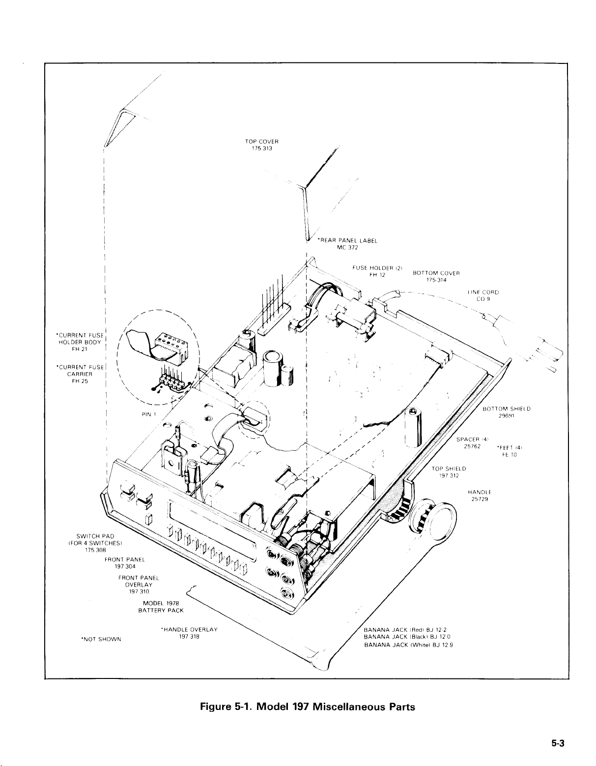
TOP
COVER
175313
,
'REAR PANEL LABEl
MC
372
'CURRENT FUSE
HOLDER BODY
FH
21
'CURRENT
FUSE
CARRIER
FH
25
I
~
I
1
1
I
Figure
5-1.
Model
197
Miscellaneous Parts
5-3
Page 44
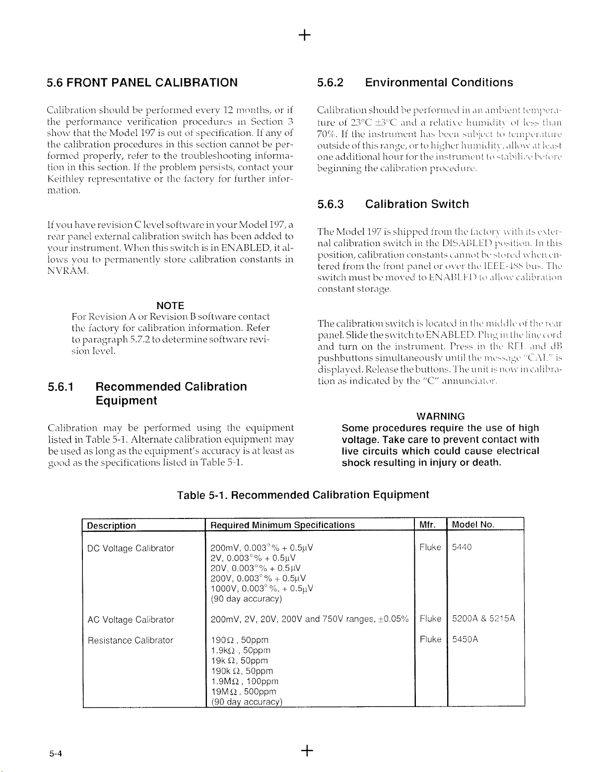
+
5.6 FRONT PANEL CALIBRATION
Calibration should
the perforiiiaiice verific,ition procedurch in Section
sliow that the
the calibration procedures in this section cannot be
formed
tion in this section.
Keithley representative or the
ini
If
rear
your instrument. When this switch is in ENABLED,
loi\~
NVI<
properly, refer to the troubleshontiiig iiiforma-
t i m.
vou
have
revision C level softivxe in your
pinel
external calibration snTitcli has
you
to
AM.
For
Re\kion
the iactory for calibration informcition. Refer
to
pxagrapli
sion lei~l.
be
bIodel
performed
197
is out
everv
12
of
specifkcition.
months, or
If
my
per-
If
the problem persists, contact your
f'ictory
pc~riiiaiiciitly store idibration constants in
NOTE
A
or
Revision B software contact
5.7.2
to determine sofhvare revi-
for further infor-
Model
been
197,
added to
it
if
3
of
al-
a
5.6.2
5.6.3
Environmental Conditions
Calibration Switch
5.6.1
Ccilibratioii may
listed in Table
be
uscd
good
Recommended Calibration
Eq
u
5-1.
as
long
as
the syccificatioiis listed in Table
Description
DC
Voltage Calibrator
AC Voltage Calibrator
Resistance Calibrator
i pmen
as
t
be
performed using
Alternate calibration equipmeiit ii~ay
the equipment's accuracy is at
Table
the
ecpipment
least
3-1.
5-1.
Recommended Calibration Equipment
Required Minimum Specifications
200mV,
2v,
2OV,
200V,
1
(90 day accuracy)
200mV, 2V, 20V, 200V and 750V ranges, +0.05%
190R
1.9k12
19k
190k
1.9MR
19M
(90 day accuracy)
0.003"%
O.OO3"%
0.003"
OOOV,
,
,
12,
(2,
12,
0.003"%
+
Yo + 0.5pV
0.003'
50ppm
50ppm
50ppm
50ppm
,
1
OOpprn
500ppm
%,
as
+
0.5LiV
+
0.5LtV
+
0.5pV
0.5~1v
WARNING
Some procedures require the use
voltage. Take care to prevent contact with
live circuits which could cause electrical
shock resulting in injury or death.
Mfr.
Fluke
Fluke
Fluke
Model
5440
5200A
5450A
No.
&
521
of
5A
high
5-4
+
Page 45
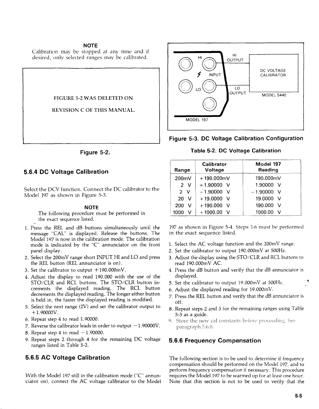
NOTE
Calibration may be stopped at any time and if
desired, only selected ranges may be calibrated.
5-2
FIGURE
WAS DELETED
ON
DC
VOLTAGE
CALIBRATOR
5440
MODEL
REVISION
C
OF
THIS
Figure
MANUAL.
5-2.
5.6.4 DC Voltage Calibration
Select the DCV function. Connect the DC calibrator to the
Model
1.
2.
3.
4.
5. Select the next range (2V) and set the calibrator output to
6.
7. Reverse the calibrator leads in order to output -1.90000V.
8.
9. Repeat steps
197
as shown
The following procedure must be performed in
the exact sequence listed.
Press the
message "CAL" is displayed. Release the buttons. The
Model 197
mode is indicated by the "C" annunciator on the front
panel display.
Select the 200mV range short INPUT
the
Set the calibrator to output +190.000mV.
Adjust the display to read 190.000 with the use of the
STO/CLR and RCL buttons. The STO/CLR button in-
crements the displayed reading. The RCL button
decrements the displayed reading. The longer either button
is held in, the faster the displayed reading is modified.
f
1.90000v.
Repeat step 4 to read 1.90000.
Repeat step 4 to read -1.90000.
ranges listed in Table 5-2.
REL
REL
is
button
in
Figure
and dB buttons simultaneously until the
now in the calibration mode. The calibration
(REL
annunciator is on).
2
through 4 for the remaining DC voltage
NOTE
5-3.
HI
and
LO
and press
MODEL
197
Figure 5-3. DC Voltage Calibration Configuration
Table
Range
200mV
2v
2v
v
20
200
v
1000
v
197
as shown in Figure
in the exact sequence listed.
1.
Select the AC voltage function and the 200mV range.
2. Set the calibrator to output 190.OOOmV at 500Hz.
3.
Adjust the display using the STO/CLR and RCL buttons to
read 190.OOOmV AC.
4.
Press the dB button and verify that the dB annunciator is
displayed.
5.
Set the calibrator to output 19.OOOmV at
6.
Adjust the displayed reading for 19.000mV.
7. Press the
off.
8.
Repeat steps 2 and 3 for the remaining ranges using Table
5-3 as a guide.
9.
Store
the
p'lragraph
5-2.
DC
Voltage Calibration
Calibrator
Voltage
+
190.000mV
+1.90000
-1.90000
+19.0000
+190.000
+1000.00
REL
button and verify that the dB annunciator is
lit317
call
5.h.S.
v
v
v
v
v
5-4.
Steps
constmts
Model
190.000mV
1.90000
-1.90000
19.0000
190.000
1000.00
1-6
hofon~
197
Reading
v
v
v
v
v
must be performed
500Hz.
pi-occLdins.
See
5.6.6 Frequency Compensation
..~
'9
5.6.5 AC Voltage Calibration
With the Model 197 still in the calibration mode ("C" annunciator on), connect the AC voltage calibrator to the Model
The following section is to be used to determine
compensation should be performed on the Model 197, and to
perform frequency compensation
requires the Model 197 to be warmed up for at least one hour.
Note that this section is not to be used to verify that the
if
necessary. This procedure
if
frequency
5-5
Page 46

'
Model 197
desired refer to Section 3 Performance Verification.
1.
Select the 750VAC range and set the calibrator to output
500.00V at 500Hz. Press the
turns on).
2. Set the calibrator to output 500.00V at 2OkHz. Verify that
the reading on the Model 197 is
REL (REL
3. Set the calibrator to output 1OO.OOV at 500Hz and select
the 200VAC range. Press the REL button
turns on).
4.
Set the calibrator to output 1OO.OOOV at 20kHz. Verify that
the reading on the Model 197 is 000.OOOV f200 counts.
Press
5. Set the calibrator to output 1O.OOOOV at 500Hz and select
the 20VAC range. Press REL
6.
Set the calibrator to output 1O.OOOOV at 20kHz. Verify that
the reading on the Model 197
Press
AC
Voltage function is within specifications.
WARN I NG
Steps
voltage. Take care not to come into contact
with live circuits that could cause personal
injury or death.
1
through 4 require the use
annunciator turns off).
REL
(REL
annunciator turns off).
REL
(REL
annunciator turns off).
REL
button
000.00
(REL
k
150 counts. Press
(REL
(REL
annunciator turns on).
is
00.0000
of
high
annunciator
annunciator
f200 counts.
2. Set the calibrator to output 500.00V at 20kHz. Adiuz
If
C103 for
annunciator turns
3.
Set the calibrator to output 1OO.OOV at 500Hz and select
the 200VAC range. Press REL
4.
Set the calibrator to output 1OO.OOV at 20kHz. Adjust
c105 for a reading on the Model 197
counts. Press REL (REL annunciator turns
5. Set the calibrator to output 1O.OOOOV
the 20VAC range. Press
6.
Set the calibrator to output
C107 for a reading on the Model 197
counts.
7. Reinstall the top cover.
a
0
reading of
off.
\
INPUT
000.00
REL
-t50
counts. Press
(REL
annunciator turns on).
of
000.OOOV
off).
at
500Hz and select
(REL
annunciator turns on).
1O.OOOOV
at 20kHz. Adjust
of
00.0000V +50
HI
OUTPUT
LO OUTPUT
REL
(REL
+50
If any of the above verifications are not met by the Model
197, the top cover must be removed and three trimmer
capacitors adjusted. The adjustments must be performed
10
within
circuit components will be close to normal operating
temperature. The three trimmer capacitors (C103, C105 and
C107) are accessible through the shield. The shield and PC
board must be secured to the bottom cover in order to prevent movement. This asssembly can be secured with two
screws and nuts (not supplied). Route the screws through the
bottom cover through the two brown spacers to the shield.
Secure the screws with the nuts. Also, use a flat blade, insulated calibration tool for all the adjustments. Perform the
following steps in the exact sequence listed.
1.
Select the 750VAC range and set the calibrator to output
500.00V at 500Hz. Press the REL button
turns on).
minutes after the top cover is removed
WARNING
Steps
voltage. Take care not to come into contact
with live circuits that could cause personal
injury or detah.
1
through 4 require the use
of
(REL
so
that the
high
annunciator
Figure
Range
200mV
200rnV"
2
20
200
MODEL
MODEL
5-4.
Table
v
v
v
197
5200A
AC
Voltage Calibration Configuration
5-3.
AC Voltage Calibration
Calibrator Calibrator Model
Voltage Frequency
190.000rnV
19.000niV
1.90000
19.0000
190.000
v
v
v
MODEL
500Hz
500Hz
500Hz
500Hz
500Hz
5215
Reading
190.000rnV
19.000rnV
1.90000 V
19.0000 V
190.000 V
197
5-6
Page 47

5.6.7
Resistance Calibration
With the Model
197
in the calibration mode
("C"
ciator on), select the ohms function and connect the calibrator to the Model
197
as shown in Figure 5-5. Four wire resistance measurements need only be done when not using
the REL feature. Use the following procedure and refer to
Table 5-4 to calibrate the ohms function.
1.
Select the
2OOQ
range and set the resistance calibrator
output zero ohms (short).
2.
Press the
REL
button on the Model 197. The
REL
ciator appears on the display and the display reads zero
(test lead compensation).
3.
Set the calibrator to output 190Q. Adjust the display using
the STO/CLR and RCL buttons
Press
REL
(REL
annunciator turns
4.
Select the 2kQ range and set the resistance calibrator to
output zero ohms (short). Press REL
turns on).
-
5.
Set the calibrator to output 1.9kQ. Adjust the display
reading
6.
Press the
turns
7.
Select the 20kQ range and set the resistance calibrator out-
of
REL
off.
1.90000kn.
button and note that the
put zero ohms (short). Press
for
a reading
off).
REL
(REL annunciator turns
(REL
REL
of
annunciator
annunciator
190.000Q.
on).
8.
Set the calibrator
reading
of
to
output 19kQ. Adjust the display
19.0000kQ. Press REL (REL annunciator turns
off).
9.
Repeat steps 7 and 8 for the
200k, 2M
and
20M
using Table 5-4 as a guide. For these ranges use the configuration shown in Figure 5-6.
annun-
to
annun-
for
a
for
a
ranges
NOTE
Four terminal resistance measurements need only be done when not using the
5.6.8
Calibration
MODEL
197
Storage
REL
feature.
MODEL 5450A
RSENSE
Figure
f
197
MODEL
5-5.
200, 2k
Calibration
INPUT
and
INPUT
HI
MODEL 5450A
INPUT
LO
SENSE
LO
20k
Four Wire Resistance
Figure
5-6,
200k, 2M
Cali brat ion
Table
Range
200
2
kQ
20
kfl
200
kQ
2MQ
20MQ
5-4.
n
and
20M
Resistance
Calibration
Resistance
190
Q
1.9
kQ
19
kQ
190
kfl
1.9 MQ
19
M
Two
Wire Resistance
Calibration
Model
190.000
1.90000
19.0000
190.000
1.90000
19.0000MQ
197
Reading
Q
kR
kQ
kQ
kQ
5-7
Page 48

Equipment
Five function DMM with 0.1
basic DCV accuracy, 10M input
impedance.
%
Use
Power supply and DC voltage checks;
analog signal tracing continuity, logic
levels.
Dual-trace, triggered sweep
oscilloscope, DC
Digital Frequency Counter
to
50MHz.
5.7 TROUBLESHOOTING
The troubleshooting instructions contained in this section are
intended for use by qualified personnel having a basic
understanding of analog and digital circuitry. The individual
should also be experienced at using electronic test equipment
as well as standard troubleshooting procedures. The information presented here has been written to assist in isolating a
defective circuit or circuit section; isolation of the specific
component is left to the technician.
The success or failure in troubleshooting an instrument such
of
as the Model 197 depends not only the skill
but also relies on accurate, reliable test equipment. Table
lists the required test equipment and specifications recommended for troubleshooting the Model 197. Other equipment
such as logic analyzers, capacitance meters (etc) could also be
helpful in difficult situations.
the technician,
5-5
5.7.1 Power Up Sequence
Digital and analog waveform checks.
Checking clock frequencies.
4.
If
no problem is found by the RAM and NVRAM checks,
the Model 197 goes into the measurement mode.
If the RAM check reveals a problem, check U121.
NVRAM check reveals a problem, check
5.7.2 (NVRAM test).
U113
and refer to
5.7.2 Self Diagnostic Program
The self diagnostic program is designed to aid the technician
in troubleshooting the Model 197. There are several tests that
may be performed using the self diagnostic program. These
tests (display, software revision level and sequential display
test) are run automatically. After this sequence the Model 197
goes into the troubleshooting mode.
To use the self diagnostic program, press and hold in the dB
button while turning on the Model 197. The following sequence occurs:
If
the
The software revision level of the Model 197 may be
displayed upon power-up by running the diagnostic program.
The diagnostic program is explained in paragraph 5.7.2.
a
When the Model 197 is turned on it goes through
sequence that is outlined as follows:
Reset-All zeroes are briefly displayed before going into
the measurement mode. During this display the Model 197
goes through a check of the RAM circuitry, and a check of
NVRAM
the
If
the
RAM
up with all zeroes. Refer to Table 2-1.
If
the
displayed:
circuitry.
circuitry has a problem, the Model 197 locks
NVRAM
test fails, the following message is
cErr
power up
1.
All LCD
2. The software revision level is then displayed (e.g.
3.
The sequential display test runs.
4.
The Model 197 goes into the troubleshooting mode.
If
the dB button is released, the instrument flags either RAM
or NVRAM self test failures, should they occur.
RAM
troubleshooting test mode.
RAM
with all zeroes displayed. Replacing U112 may correct the
problem.
Non-Volatile RAM Test-If the NVRAM test fails, the
following message is displayed:
digits and annunciators turn on.
Al).
If
neither
nor NVRAM fails, the instrument defaults to the
Test-If the RAM test fails, the Model 197 locks up
cErr
Page 49

"This is a message indicating that the instrument is not
calibrated properly, since calibration constants are stored in
NVRAM. The Model 197 remains at this point
but operation may be restored
ing either the
"C" annunciator indicates that the unit failed the NVRAM
test.
At this point try calibrating the instrument with the constants
already entered by simultaneously pressing
the CAL message is displayed. Then release the
buttons. Simultaneously press the
until the STOR message is displayed.
indicating that the NVRAM is probably good, a full calibra-
tion is required.
chip,
recalibrated after the problem is corrected.
Sequential Display Test-Segments and annunciators are
sequentially displayed in eight steps. Use Figure
ment identification. The steps are
1.
The "a" segments of the digits, the dB and V annunciators
are displayed.
2. The "b" segments
3.
The "c" segments of the digits are displayed.
4.
The "d" segments
(mA)
5. The "e" segments of the digits are displayed. Also, the
minus sign,
6.
The
AUTO, BAT, m(mV) and c annunciators are displayed.
7.
The
and k annunciators are displayed.
8.
The decimal points, most significant digit and the STO,
and A annunciators are displayed.
REL,
dB
or
If
the error persists try replacing the NVRAM
U113.
Again the Model 197 must be completely
of
the digits are displayed.
of
RCL
and
RMT
REL,
M and Q annunciators are displayed.
"f"
segments of the digits are displayed. Also, the
"g"
segments of the digits are displayed. Also, the AC
for
troubleshooting by press-
DATA Logger buttons. The flashing
REL
and dB buttons again
If
as
the digits are displayed. Also, the m
annunciators are displayed.
if
the test fails,
REL
and dB until
REL
and dB
the error is corrected,
5-7
for
seg-
follows:
Troubleshooting Test Modes-The troubleshooting mode
designed to switch on various switching
relays and logic levels to allow signal tracing through the instrument. The first displayed mode reflects the selected function and range. For example; assume that
In this case,
0 is the test number.
u
corresponds to the volts function.
1
corresponds to the 200mV range.
The test number can be changed by pressing in the dB button.
Table
5-6
lists test modes for all functions and ranges.
Troubleshooting consists
and using the data found in Table
cuit.
NOTES:
1.
When a different function
ton must be pressed and held in to update the display with
the corresponding test mode.
2. Do not use AUTO when in AC
3.
Use AUTO when checking circuitry on the 20M and
200MQ range
5.7.3
Power Supply and Battery Pack (Model
1978)
Table 5-7 shows the various checks that can be made to the
power supplies
p
normal voltage checks, it is a good idea to check the various
supplies with an oscilloscope for signs of noise
(006,
Checks
of
the Model 197 and 1978. In addition
of
selecting the desired test mode
5-6
or
range is selected, the dB but-
or
106,
206,
306
FETs,
transistors,
"Oul"
is displayed.
to signal trace the cir-
DC volts.
and
406).
or
oscillations.
to
is'
the
Figure
a
fl-I
9
C
el
5-7.
Segment Identification
I
d
5.7.4
A/D Converter and Display
Make sure the A/D converter and display are operating
perly BEFORE attempting to troubleshoot the signal condi-
tioning circuits. Check these circuits using the information
Table 5-8 and 5-9.
5.7.5
Signal Conditioning
These circuits can be checked by using the diagnostic pro-
gram (troubleshooting modes). See paragraph 5.7.2.
refer to Table 5-6.
pro-
in
Also,
5-9
Page 50

Table
5-6.
Model
197
Troubleshooting Mode
Function
and
Range
200rnVDC
Test
Mode
ou
lul
2u 1
3u
2VDC ou2
1 u2
2u2
3u2
20VDC Ou3
1
u3
2u3
3u3
200VDC
Ou4
1 u4
2u4
3u4
1 kVDC
Ou5
1
u5
2u5
3u5
200rnVAC ou 1
lul
2u
3u 1
2VAC ou2
1 u2
2u2
3u3
20VAC Ou3
1 u3
2u3
3u3
200VAC Ou4
1
u4
2u4
3u4
750VAC Ou5
1 u5
2u5
3u5
DCA
All
Ranges
OA 1 -0A6
1 A1 -1 A6
2A 1 -2A6
3A1-3A6
200Q
00
101
20 1
30
1
1
1
1
1
DC
Gain
u102
XI0
XI0
XI0
XI0
Amp
XI
XI
XI
XI
x1
XI
XI
XI
XI
XI
XI
XI
XI
XI
XI
XI
XI
XI
XI
XI
XI
XI
XI
XI
XI
XI
XI
XI
XI
XI
XI
XI
XI
XI
XI
XI
XI
XI
XI0
XI
XI
XI0
XI
XI
AC
Amp
Gain
U104
x5
x5
x5
x5
XI
XI
XI
XI
XI
XI
XI
XI
XI
XI
XI
XI
XI
XI
XI
XI
Multiple8
On
FET
0111
01 12
01 13
0112
0111
01 12
0113
0112
0111
01
10
01 13
01 12
0111
0110
0113
0112
0111
01 10
01 13
0112
0111
01 12
01 13
01 12
0111
01 12
01 13
0112
0111
0112
0113
01 12
0111
0112
01 13
01
12
0111
01
12
0113
01 12
0111
0112
01 13
01 12
0113
0112
0111
0110
Range
Transistor On
0104, 0105
0104, 0105
0104, 0105
0104. 0105
0104, 0105, 0106, 0107
0104, 0105, 0106, 0107
0104, 0105, 0106, 0107
0104, 0105, 0106. 0107
0104, 0105, 0109, 0108
0104, 0105, 0109, 0108
0104, 0105, 0109, 0108
0104, 0105, 0109, 0108
0104-0107, 0118
0104-0107, 0118
0104-0107, 0118
0104-0107, 0118
0104-0107, 0118
0104-0107, 0118
0104-0107, 0118
0104-0107. 0118
0104, 0105, 0106, 0107
0104, 0105, 0106, 0107
0104, 0105, 0106, 0107
0104, 0105, 0106, 0107
0104, 0105, 0108, 0109
0104, 0105, 0108, 0109
0104, 0105, 0108, 0109
0104. 0105. 0108, 0109
0104, 0105
0104, 0105
0104, 0105
0104. 0105
0104, 0105
0104, 0105
0104, 0105
0104. 0105
Range Control
:
3
Levels
PA0
0
0
0
0
0
0
0
0
1
0
0
0
~
0
0
0
0
-
0
0
0
0
__
0
0
0
0
0
0
0
0
0
0
0
0
~
~
0
0
0
0
0
0
0
___
0
0
0
0
0
1
0
1
0
0
0
0
0
0
0
1
0
~
1
1
0
0
~
On
U
0
1
I0
010
Ojl
010
10
00
01
00
10
00
01
0
0
~
1
0
0
0
1
0
0
0
~
~
1
0
0
0
1
0
0
0
~
0
0
1
0
~
1
0
0
0
1
0
0
0
~
~
0
1
0
0
1
0
0
0
~
0
0
1
0
~
1
0
0
0
1
0
0
0
~
~
0
1
0
0
0
1
0
0
~
5-10
Page 51
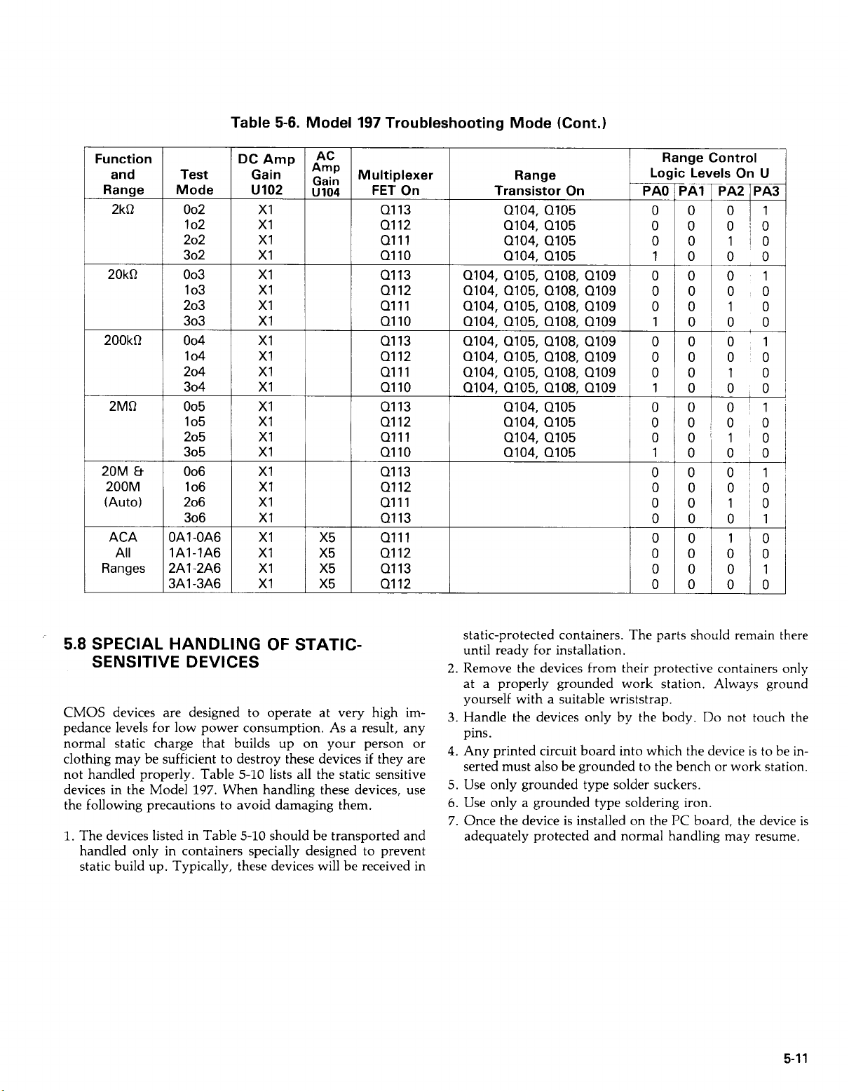
Table
5-6.
Model
197
Troubleshooting Mode (Cont.)
Function
and
Range
2kQ
20kQ
200kQ
2MQ
20M
Et
200M
(Auto)
ACA
All
Ranges
Test
Mode
002
102
202
302
003
103
203
303
004
104
204
304
005
105
205
305
006
106
206
306
OA 1 -0A6
1
A1
-1
A6
2A
1
-2A6
3A
1
-3A6
DC Amp
Gain
u102
XI
XI
XI
XI
XI
XI
XI
XI
XI
XI
XI
XI
XI
XI
XI
XI
XI
XI
XI
XI
XI
XI
XI
XI
AC
AmD
Gain
U104
x5
x5
x5
x5
M
ul
ti
plexer Range
FET On Transistor On
Q104, Q105
0104, 0105
Q104, 0105
Q110 0104, Q105
01
13
0104, 0105,
Q108,
Q112
Q111
Q110
Q113
Q112
Q111
0104, 0105,
Q104, 0105,
0104, 0105,
0108,
Q108,
Q108,
Q110
01
13
Q112
0111
Q110
Q104, Q105
Q104, 0105
Q104, Q105
0104. 0105
Q113
01 12
Qlll
Q113
Q111
Q112
Q113
Q112
Q109
Q109
Q109
Q109
Range Control
~
0
0
00
00
00
10
01
00
10
00
01
00
10
00
0
'1
I
0
01
1
01
0
01
5.8
SPECIAL HANDLING
OF
STATIC-
SENSITIVE DEVICES
CMOS
pedance levels for low power consumption. As a result, any
normal static charge that builds up on your person
clothing may be sufficient to destroy these devices if they are
not handled properly. Table 5-10 lists all the static sensitive
devices in the Model 197. When handling these devices, use
the following precautions to avoid damaging them.
1.
devices are designed to operate at very high im-
or
The devices listed in Table 5-10 should be transported and
handled only in containers specially designed to prevent
static build up. Typically, these devices will be received in
static-protected containers. The parts should remain there
until ready for installation.
2.
Remove the devices from their protective containers only
at a properly grounded work station. Always ground
yourself with a suitable wriststrap.
3.
Handle the devices only by the body.
pins.
4.
Any printed circuit board into which the device is to be inserted must also be grounded to the bench or work station.
5.
Use only grounded type solder suckers.
6.
Use only a grounded type soldering iron.
7. Once the device is installed on the
adequately protected and normal handling may resume.
Do
not touch the
PC
board, the device is
5-1
1
Page 52

Table
itep
Item/ComDonent
~
1
5102
F102 Line Fuse
2
Line Cord
3
4
Power ON/OFF switch pin 6
5
U109 pin 2
U109 pin 3
6
0126 collector or U116 pin 7
7
Power ON/OFF switch pin 12
8
U107 pin 2
9
10
U107 pin 3
11
Q128 Emmitter
12
U116 pin 3
U116 pin 2
13
Q126 Emitter
14
0123 Emitter or J1009 pin 7
5"
*
16*
Q101 Base
17"
UlOl pin 8
U102 pin 7
18"
*Battery option (1978) checks.
""If Q123 is replaced, be sure that the device is properly seated on the mother board
IEEE
board (if installed).
5-7.
Power Supply and Battery Pack (Model
Reauired Condition
Set to 115V or 230V as required.
Continuity
Plugged into proper line recep-
tacle; power
+
13V to + 16.5V
+6.4
+6.4 +5%
+1
ov
-15V *lo%
-6.4V *lo%
-6.4V +lo%
-9.ov, +5%
+5v &5%
+5v *5%
+5.0V
+5.0V f 10%
0.6V while charging. Power
switch
>
10.8V Line cord disconnected,
battery pack charged and power
on
+
5V with batteries charged.
f5%
f1
0%
f5%
off.
on.
1978)
Remarks
S102 is externally accessible from rear panel.
+
V power for regulator circuitry.
Virtual Reference.
Reference Zener.
+
1ov Supply
-V power for regulator circuitry.
Inverting input for U107.
Low noise negative supply reference.
-9v Supply
+
5V supply reference.
Inverting input for U116.
+
5V analog supply.
+
5V digital supply.
Current Sink
Voltage Inverter
Voltage Comparator
Checks
so
that
it
will not touch the
Step Item/Component Required Condition
12 P1006, pin 5
3 P1006, pin 6
4 P1006, pin 7 +5v +5%
5 P1006, pin 2 81.92kH.z
6 P1006, pin 1
7 P1006, pin 12
8 P1006, pin 13 OV to +5V Pulses
9 P1006, pin 14
10 LCD Verify that thet LCD is properly posi-
11 Connector (P1006) Check that connector is not reversed.
12 Strip Connector Verify that they are positioned properly.
5-12
Turn on power; select the 2V range.
+
3.3v
+
1.66V
OV to +5V Pulses
OV to +5V Pulses
+5V to OV Pulses
tioned.
Remarks
Vlcd 1
Vlcd2
Power to Display
Clock
Data From pp.
Data From pp.
Data From yp.
Data From pp.
Page 53

Table 5-9. A/D
-
Step
ltem/ComDonent I Reauired Condition
___
1
2
U124 pin 38
U119 pin 10
3
U119 pin 6
4
U119 pin 5
5
U119 pin 7
6
7
U119 pin 12
U118 pin 6
8
UllO pin 6
9
U108B pin 7
10
U117 pin 6
11
U105A pin 15
12
U105A pin 10
13
U117B pin 9
14
~
Turn on power; select 2VDC range.
Short the input.
3.276800MHz Clock
655.36kHz Clock
81.92kHz Clock
40.96kHz Clock
163.84.kHz Clock
1.28kHz Clock
+
5V to = OV pulse train, 3psec in
duration every 22psec. (Set
signal to end charge balance pulse.)
Integrator Waveform.
Variable waveform OV to
1
Variable pulse train, OV to + 5V
Variable pulse train, OV to +5V.
4msec pulses approximately every
150msec. OV to +5V.
50msec and 100msec pulses
Converter/Microcornputer
Crystal Frequency (Y101)
AID tirnebase and
address strobe.
Clocks for U117A.
generator signal.
Q4
Timebase for real time
pP
S1 input
+
5V.
Comparator Output
Charge Balance Current
Checks
Remarks
pP
Minimum pulse
Generates set for
U117A. (proper phase
and Q3 required).
interrupt.
of
U118B.
(Charge Balance)
Control.
U124 Timer Input
Single Slope Control
Line
Integrator charge
Balance Control
of
Table 5-10. Model 197 Static Sensitive Devices
Circuit Designation
0104, Q107
(2108, QllO
Q111, (3112
Q113
u101
U105
U107
U113
U114
U115
U117
U118
u119
u120
u121
u122
U123
U124
Keithley Part
TG-139
TG-I39
TG-139
TG-I39
IC-415
IC-283
IC-347
IC-353
LSI-61
IC-143
IC-337
IC-341
IC-348
IC-351
LSI-62
197-800-**
IC-338
LSI-60
No.
5-13/5-14
Page 54

SECTION
REPLACEABLE PARTS
6.1
INTRODUCTION
This section contains replacement parts information, component location drawings and schematic diagrams for the Model
197 and Model 1978.
6.2
REPLACEABLE PARTS
Parts are listed alpha-numerically in order of the schematic
designation. Table 6-1 contains parts list information for the
mother board. Table 6-2 contains parts list information for
the display board. Parts list information for the Model 1978
Battery Pack is contained in Table 6-3.
6.3
ORDERING INFORMATION
To
place an order, or to obtain information concerning
replacement parts, contact your Keithley representative
the factory. See the inside front cover for addresses. When
ordering include the following information:
1.
Instrument Model Number
2. Instrument Serial Number
3.
Part Description
4.
Circuit Designation
5.
Keithley Part Number
(if
applicable)
or
6
6.4
FACTORY SERVICE
If
the instrument is to be returned to the factory for service,
photo copy and complete the service form which follows this
section and return
6.5
SCHEMATIC DIAGRAMS AND
COMPONENT LOCATION DRAWINGS
The component location drawings and schematic diagrams,
are presented as follows:
Figure 6-2. Model 1978 Battery Pack, Component Location
Drawing, Dwg. No. 1978-100.
Figure 6-3. Mother Board, Component Location Drawing,
Dwg.
NO.
197-100.
Figure 6-4. Display Board, Component Location Drawing,
Dwg.
NO.
197-110.
Figure 6-5. Mother Board, Schematic Diagram, Dwg.
197-106.
Figure 6-6. Display Board, Schematic Diagrm, Dwg.
197-116.
Figure 6-7. Model 1978 Battery Pack, Schematic Diagram,
Dwg. NO. 1978-106.
it
with the instrument.
No.
No.
If
an additional instruction manual is required, order the
manual package (Keithley Part Number 197-901-00). The
manual package includes an instruction manual and all pertinent addenda.
6-1
Page 55

-
/’.
11
.
-
I
WINDOW BEZEL
J
,RETAINER
175-305
MASK
175 306
__
LCD
DD-36
175-307
6-2
Figure
6-1.
Display
Assembly
Exploded
View
Page 56

Table
6-2.
Display Board, Parts
List
Schematic
Desig.
DS-201
PI006
u201
Schematic
Desig.
BTlOl
ClOl
c102
CR101
PI009
R101
R102
R103
R104
R105
0101
U101"
u102
*Static Sensitive Device
Description
5 1/2 Digit Liquid Crystal Display (LCD)
Cable Assembly (14 Conductor)
LCD Controller/ Driver
Retainer, Strip Connector
Strip Connector (2 required)
LCD Mask
Window Bezel
Switch Pad, Conductive Touch
DescriDtion
Battery Assembly, 12.0V Sealed Rechargeable NiCad
Capacitor, 250pF, 25V, Aluminum Electrolytic
Capacitor, IOpF, 25V, Aluminum Electrolytic
Rectifier, Schottky Barrier, 1 N5820
Cable Assembly, 10 Conductor
Resistor, 4.7f2, lo%,
Resistor, 4.7Q2,
Resistor, 44.2k, 1
Resistor, 37.4k, 1
Resistor, 1.2M, 5%, 1 /4W, Composition
Transistor, NPN, High Voltage (TIP-49)
Voltage Converter, S17661 CJ
Voltage Comparator, LM393
Heat Sink used on UlOl
Standoff (Battery Board to Shield)
Table
6-3.
IW,
YO,
1 /4W, Composition
%,
1 /8W, Metal Film
YO,
1 /8W, Metal Film
Model
Fixed, Fusible, Wound
1978
Battery Pack, Parts List
Location
Sch Pcb
D2 D3
B4 C4
D3 C4
Location
;ch Pcb
-
B3
D2 E4
D3 C4
D2 D4
D2 B1
E2 C3
El
C2
E3 E3
E3 E4
D3 E3
D3 C2
D3 04
D3 E3
D3
-
D3
-
Keithley
Part
No.
DD-36
CA-30-2
LSI-59
175-307
CS-460-2
175-306
175-305
175-308
Keithley
Part
No.
BA-40
C-314-220
C-314-10
R
F-53
CA-27-1
R
-334-4.7
R-76-4.7
R
-88-44.2k
R
-88-37.4k
R-76-1.2M
TG-I37
IC-340
1C-343
H
5-28
6-6
Page 57

Figure
6-2.
Model
Drawing, Dwg.
1978 Battery Pack, Component Location
No.
1978-100
6-7/64
Page 58

Figure
6-3.
Mother Board, Component Location Drawing,
Dwg.
No.
197-100
(sheet
1 of
2)
6-916-10
Page 59

Figure
6-3.
Mother Board, Component Location Drawing,
Dwg.
No.
197-100
(sheet 2 of
2)
6-11 /6-12
Page 60

Figure
6-4,
Display Board, Component Location Drawing,
Dwg.
NO.
197-110
6-1316-14
Page 61

Figure 6-5. Mother Board, Schematic Diagram, Dwg.
197-106 (sheet 1
of
21
6-1516-16
No.
Page 62

Figure
6-5.
Mother Board, Schematic Diagram, Dwg.
197-106
(sheet
2
of
2)
No.
6-17/6-18
Page 63

Figure
6-6.
Display Board, Schematic Diagram, Dwg.
197-116
6-19/
No.
6-20
Page 64

Figure 6-7. Model 1978 Battery Pack, Schematic Diagram,
Dwg.
NO.
1978-106
6-21
16-22
Page 65

+
Instruments Division, Keithley Instruments, Inc.
WEST GERMANY:
GREAT BRITAIN:
FRANCE
NETHERLANDS
SWITZERLAND.
AUSTRIA
ITALY:
Keithley Instruments GmbH
Keithley Instruments, Ltd. The Minster
Keithley Instruments SARL 3 Allee
Keithley Instruments BV
Keithley Instruments SA Kriesbachskr. 4 8600 Dubendorf
Keithley Instruments GesmbH Rosenhugelstrasse
Keithley Instruments SRL Viale
.
Heiglhofstr.
des Garays B.P.
Avelingen West
S.
Girnignano
28775 Aurora
5
-
Munchen
58,
Porhnan Road Reading, Berkshire
49 4202
4/A 20146
Road Cleveland,
70 089-71002-0
60 91124
MS Gorinchem
01-821-9444
12
A-1120
Milano
Palaiseau/Z.I.
P.O.
Vienna
02-4120360
+
Telex:
52-12160
KG
1-6-0115 155
Box
559 4200
Telex:
(0222) 84 65
or
Ohio
3
IEA
828 472
48
02-4156540
Fax:
AN
Gorinchem
Fax:
Telex:
44139
089-7100259
011 44
731
Telex:
0222-315366
131677.
Fax:
(216)
575
6h6
600 933
01830-35333
Fax:
024121249
248-0400
Fa\.
fkx
(0222)
tLz035')7
Fax:
Oil
4%
731
l-h-~lll772h
T&\.
21
2-16-6168
5%
4hY
h8-I.
FJ\
lilS3O-.~OX?I
 Loading...