

Page 1
SERVICE MANUAL
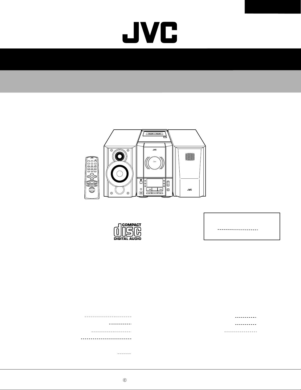
MICRO COMPONENT SYSTEM
UX-V30
AUTO TAPE SELECT OR
TAPE
AUTO REVERSE
UX-V30
UX-V30
REMOTE CONTROL RM-RXUV5R
DIMMER SLEEP
DISPLAY FM MODE MD/AUX
AUTO
AHB PRO
PRESET
PROGRAM RANDOM REPEAT
BASS TREBLE CANCEL
UP
SET
DOWN
TUNER
TAP E
BAND
VOLUME
COMPACT
DIGITAL AUDIO
VERTICAL DISC
STANDBY/ON
PHONES
MICRO COMPONENT SYSTEM
MD/
AUX
REC
REV.
MODE
TAPE FM/AM CD
DOWN UPMULTI CONTROL
LOADING MECHANISM
UX-V30
AHB
PRO
VOLUME
TIMER
CLOCK
CD
OPEN/CLOSE
CD
CD
Area Suffix
UF
China
Contents
Safety precautions
Important for laser products
Disassembly method
Main adjustment
Flow of functional operation
until TOC read
This service manual is printed on 100% recycled paper.
COPYRIGHT 2000 VICTOR COMPANY OF JAPAN, LTD.
1-2
1-3
1-4
1-14
1-18
Maintenance of laser pickup
Replacement of laser pickup
Description of major ICs
1-19
1-19
1-20
No.20888
Dec. 2000
1-1
Page 2
UX-V30
1. This design of this product contains special hardware and many circuits and components specially
2. Alterations of the design or circuitry of the product should not be made. Any design alterations of
3. Many electrical and mechanical par ts in the products have special safety-related characteristics.
4. The leads in the products are routed and dressed with ties, clamps, tubings, barriers and the
Safety Precautions
for safety purposes. For continued protection, no changes should be made to the original design
unless authorized in writing by the manufacturer. Replacement parts must be identical to those
used in the original circuits. Services should be performed by qualified personnel only.
the product should not be made. Any design alterations or additions will void the manufacturer`s
warranty and will further relieve the manufacture of responsibility for personal injury or proper ty
damage resulting therefrom.
These characteristics are often not evident from visual inspection nor can the protection afforded
by them necessarily be obtained by using replacement components rated for higher voltage,
wattage, etc. Replacement parts which have these special safety characteristics are identified in
the Parts List of Service Manual. Electrical components having such features are identified by
shading on the schematics and by ( ) on the Parts List in the Service Manual. The use of a
substitute replacement which does not have the same safety characteristics as the recommended
replacement parts shown in the Parts List of Service Manual may create shock, fire, or other
hazards.
like to be separated from live parts, high temperature parts, moving parts and/or sharp edges
for the prevention of electric shock and fire hazard. When service is required, the or iginal lead
routing and dress should be observed, and it should be confirmed that they have been returned
to normal, after re-assembling.
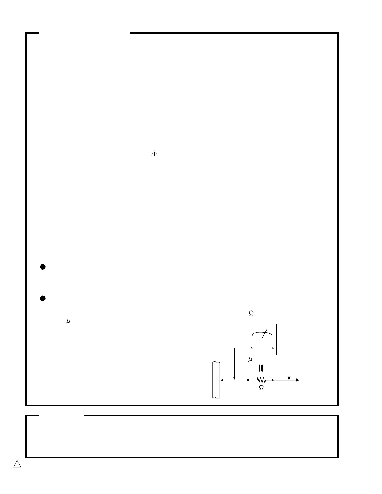
5. Leakage currnet check (Electrical shock hazard testing)
After re-assembling the product, always perform an isolation check on the exposed metal parts
of the product (antenna terminals, knobs, metal cabinet, screw heads, headphone jack, control
shafts, etc.) to be sure the product is safe to operate without danger of electrical shock.
Do not use a line isolation transformer during this check.
Plug the AC line cord directly into the AC outlet. Using a "Leakage Current Tester", measure
the leakage current from each exposed metal parts of the cabinet , particularly any exposed
metal part having a return path to the chassis, to a known good earth ground. Any leakage
current must not exceed 0.5mA AC (r.m.s.)
Alternate check method
Plug the AC line cord directly into the AC outlet. Use an AC voltmeter having, 1,000 ohms
per volt or more sensitivity in the following manner. Connect a 1,500 10W resistor paralleled by
a 0.15 F AC-type capacitor between an exposed
metal part and a known good earth ground.
Measure the AC voltage across the resistor with the
AC voltmeter.
Move the resistor connection to eachexposed metal
part, par ticularly any exposed metal part having a
return path to the chassis, and meausre the AC
voltage across the resistor. Now, reverse the plug in
the AC outlet and repeat each measurement. voltage
measured Any must not exceed 0.75 V AC (r.m.s.).
This corresponds to 0.5 mA AC (r.m.s.).
0.15 F AC TYPE
1500 10W
Good earth ground
AC VOLTMETER
(Having 1000
ohms/volts,
or more sensitivity)
Place this
probe on
each exposed
metal part.
Warning
1. This equipment has been designed and manufactured to meet international safety standards.
2. It is the legal responsibility of the repairer to ensure that these safety standards are maintained.
3. Repairs must be made in accordance with the relevant safety standards.
4. It is essential that safety critical components are replaced by approved parts.
5. If mains voltage selector is provided, check setting for local voltage.
CAUTION
!
1-2
Burrs formed during molding may be left over on some parts of the chassis. Therefore,
pay attention to such burrs in the case of preforming repair of this system.
Page 3
Important for laser products
UX-V30
1.CLASS 1 LASER PRODUCT
2.DANGER : Invisible laser radiation when open and inter
lock failed or defeated. Avoid direct exposure to beam.
3.CAUTION : There are no serviceable parts inside the
Laser Unit. Do not disassemble the Laser Unit. Replace
the complete Laser Unit if it malfunctions.
4.CAUTION : The compact disc player uses invisible
laserradiation and is equipped with safety switches
whichprevent emission of radiation when the drawer is
open and the safety interlocks have failed or are de
feated. It is dangerous to defeat the safety switches.
VARNING : Osynlig laserstrålning är denna del är öppnad
och spårren är urkopplad. Betrakta ej strålen.
VARO : Avattaessa ja suojalukitus ohitettaessa olet
alttiina näkymättömälle lasersäteilylle.Älä katso
säteeseen.
5.CAUTION : If safety switches malfunction, the laser is able
to function.
6.CAUTION : Use of controls, adjustments or performance of
procedures other than those specified herein may result in
hazardous radiation exposure.
CAUTION
!
Please use enough caution not to
see the beam directly or touch it
in case of an adjustment or operation
check.
ADVARSEL : Usynlig laserstråling ved åbning , når
sikkerhedsafbrydere er ude af funktion. Undgå
udsættelse for stråling.
ADVARSEL : Usynlig laserstråling ved åpning,når
sikkerhetsbryteren er avslott. unngå utsettelse
for stråling.
REPRODUCTION AND POSITION OF LABELS
WARNING LABEL
1-3
Page 4
UX-V30
Disassembly method
<Main body>
Removing the rear cover
(See Fig.1 and 2)
1.
Remove the eight screws A attaching the rear cover
on the back of the body.
2.
Remove the two screws B attaching the rear cover
on the bottom of the body.
3.
Unlock the speaker terminal and the antenna
terminal, then remove the rear cover backward with
releasing the hooks.
Removing the side panels
(See Fig.3 and 4)
Prior to performing the following procedure, remove
the rear cover.
A
A
A
A
A
Rear cover
Fig.1
B
Rear cover
1.
Move the side panels in the direction of the arrow
and remove them backward.
Side panel (R)
B
Fig.2
Side panel (L)
1-4
Fig.3Fig.4
Page 5
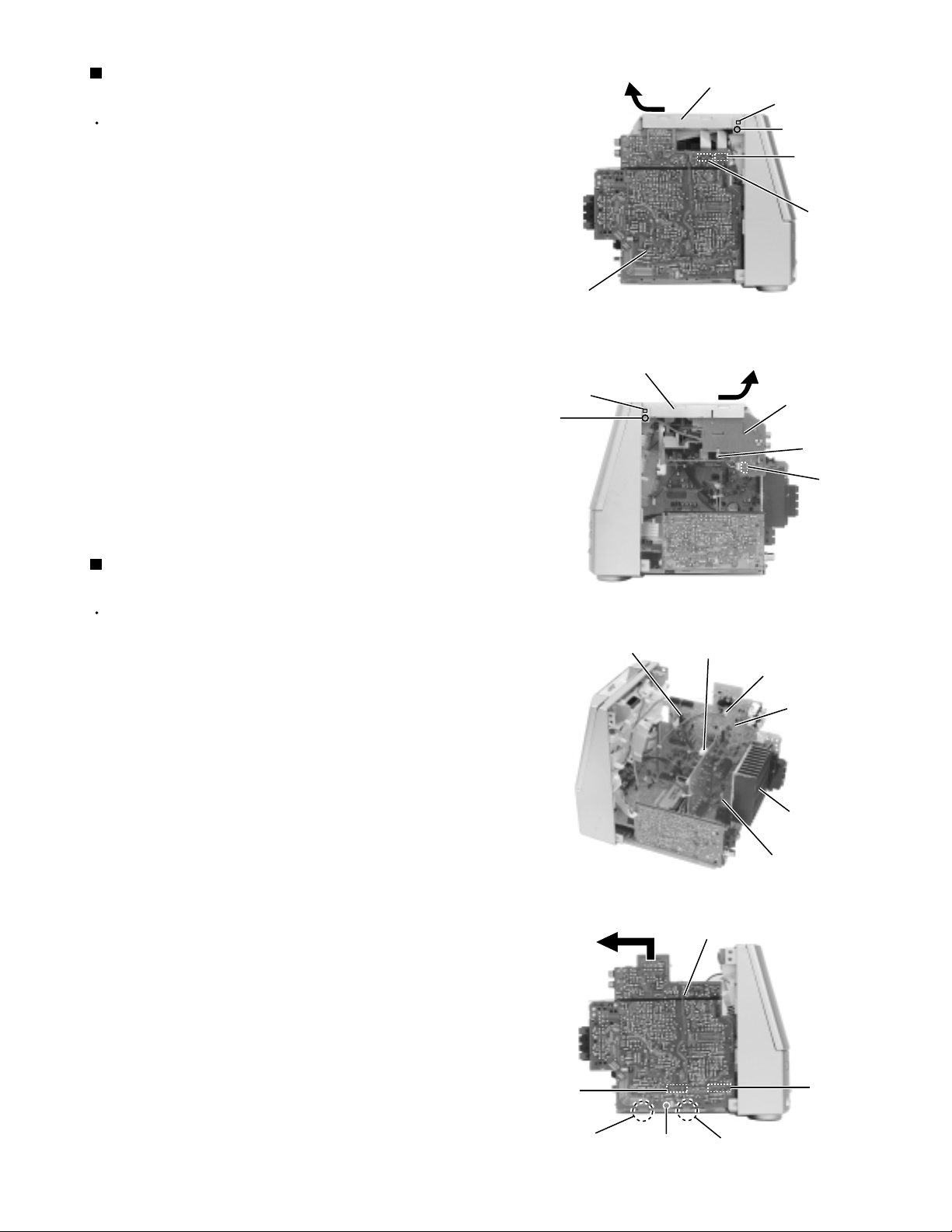
UX-V30
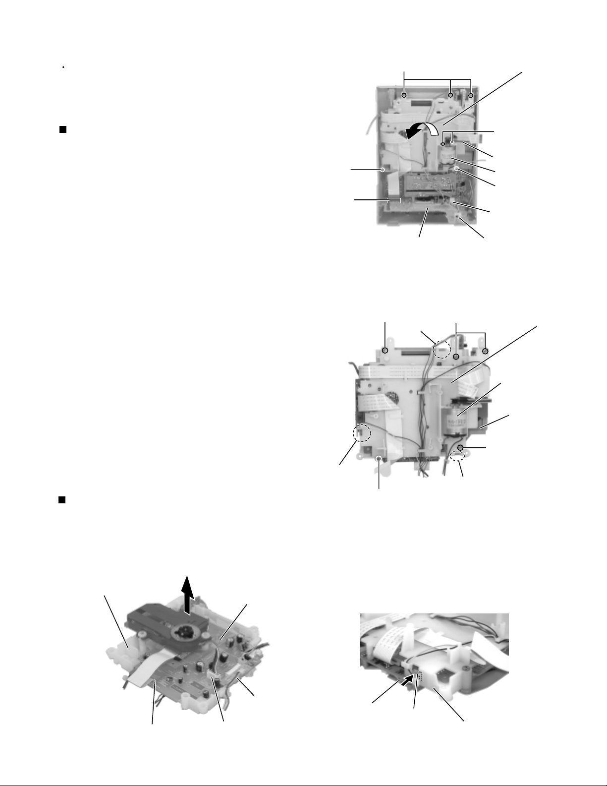
Removing the cassette mechanism
assembly (See Fig.5 and 6)
Prior to performing the following procedure, remove
the rear cover and the side panels.
1.
Disconnect the card wires from connector CN304
and CN305 on the main board on the left side of the
body.
2.
Disconnect the harness from connector CN309 on
the Opt, Dig.out board on the right side of the body.
Cut off the band fixing the harness.
3.
Remove the two screws C attaching the cassette
mechanism assembly on both sides of the body and
release the two joints a.
4.
Remove the cassette mechanism assembly in the
direction of the arrow.
Cassette mechanism assembly
Main board
Fig.5
Cassette mechanism assembly
Joint a
C
Joint a
C
CN304
CN305
Opt, Dig.out board
Band
CN309
Removing the main board / the heat sink
(See Fig.7 to 9)
Prior to performing the following procedure, remove
the rear cover, the side panels and the cassette
mechanism assembly.
1.
Disconnect the card wire from connector CN303 and
the harness from CN306 and CN307 on the main
board respectively.
2.
Disconnect the harness from connector CN902 on
the power transformer.
3.
Remove the screw E attaching the main board on
the right side of the body.
4.
Remove the screw F and the two screws G
attaching the heat sink on the back of the body.
ATTENTION:
5.
Disconnect connector CN301 and CN302 on the
main board from the main body. Remove the main
board upward by releasing the two joints b in the
lower part of the main board.
The heat sink can be removed even if
the main board is attached to the body.
CN303
Fig.6
Transformer board
CN902
CN307
Main board
Heat sink
CN306
Fig.7
Main board
CN302
Joint b
E
CN301
Joint b
Fig.8
1-5
Page 6
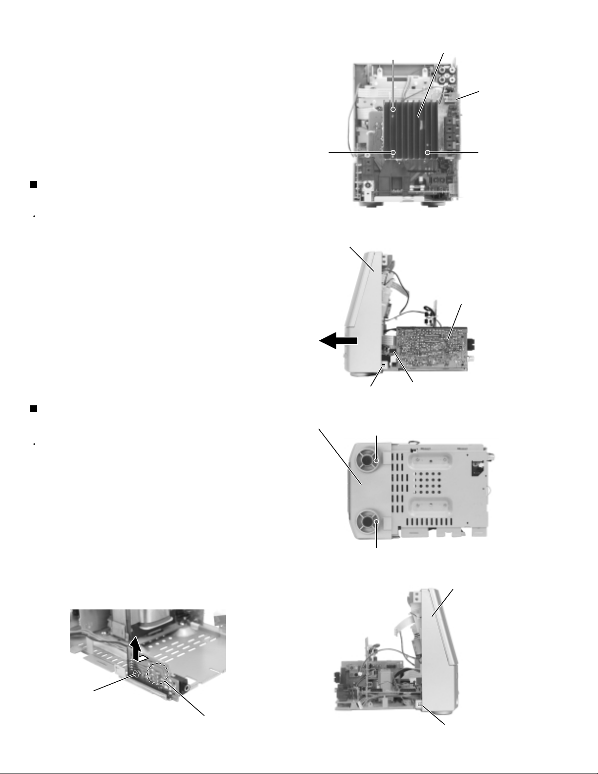
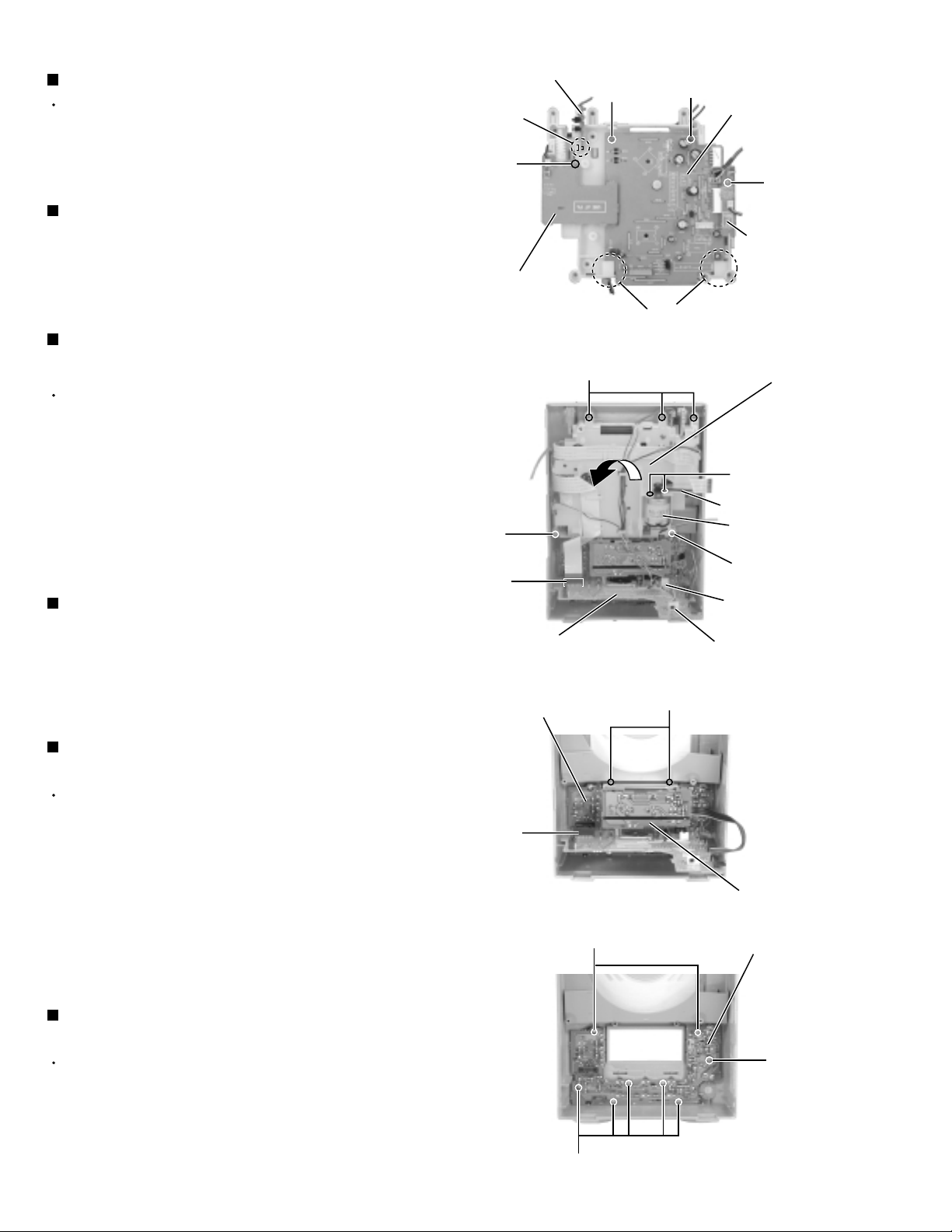
UX-V30
Removing the front panel assembly
(See Fig.10 to 12)
Prior to performing the following procedure, remove
the rear cover, the side panels, the cassette
mechanism assembly and the main board.
1.
Disconnect the card wire from connector CN732 on
the LCD board.
2.
Remove the two screws D attaching the front panel
assembly on the bottom of the body.
F
Front panel assembly
G
Heat sink
Main board
G
Fig.9
Tuner & function board
3.
Release the two joints c on the lower right and left
sides of the body. Pull out the front panel assembly
toward the front.
Removing the head phone board
(See Fig.13)
Prior to performing the following procedure, remove
the rear cover, the side panels, the cassette
mechanism assembly, the main board and the front
panel assembly.
1.
Remove the plastic rivet attaching the head phone
board and release the joint d.
Joint c
Front panel assembly
D
D
LCD board
Fig.10
Fig.11
CN732
Front panel assembly
1-6
Plastic rivet
Joint d
Fig.12Fig.13
Joint c
Page 7
Removing the tuner & function board
(See Fig.14)
Prior to performing the following procedure, remove
the rear cover, the side panels and the cassette
mechanism assembly.
1.
Disconnect the card wire from connector CN1 on the
tuner & function board.
2.
Remove the screw H attaching the tuner & function
board.
UX-V30
3.
Release the two joints e and the joint f of the tuner &
function board.
Removing the power transformer
(See Fig.15)
Prior to performing the following procedure, remove
the rear cover, the side panels and the cassette
mechanism assembly.
1.
Disconnect the harness from connector CN902 on
the power transformer.
2.
Disconnect the harness from connector CN901 on
the AC supply board.
3.
Remove the four screws I attaching the power
transformer.
CN1
Main board
CN902
I
H
J
Joint e
Heat sink
Tuner
& function board
Joint f
Fig.14
AC supply board
J
CN901
I
Removing the AC supply board
(See Fig.15)
*Prior to performing the following procedure, remove
the rear cover, the side panels and the cassette
mechanism assembly.
1.
Disconnect the harness from connector CN901 on
the AC supply board.
2.
Remove the screw F attaching the heat sink on the
back of the body (Refer to Fig.9).
3.
Remove the two screws J attaching the AC supply
board.
ATTENTION:
To remove the AC supply board
efficiently, remove the main board in
advance.
Power transformer board
Fig.15
1-7
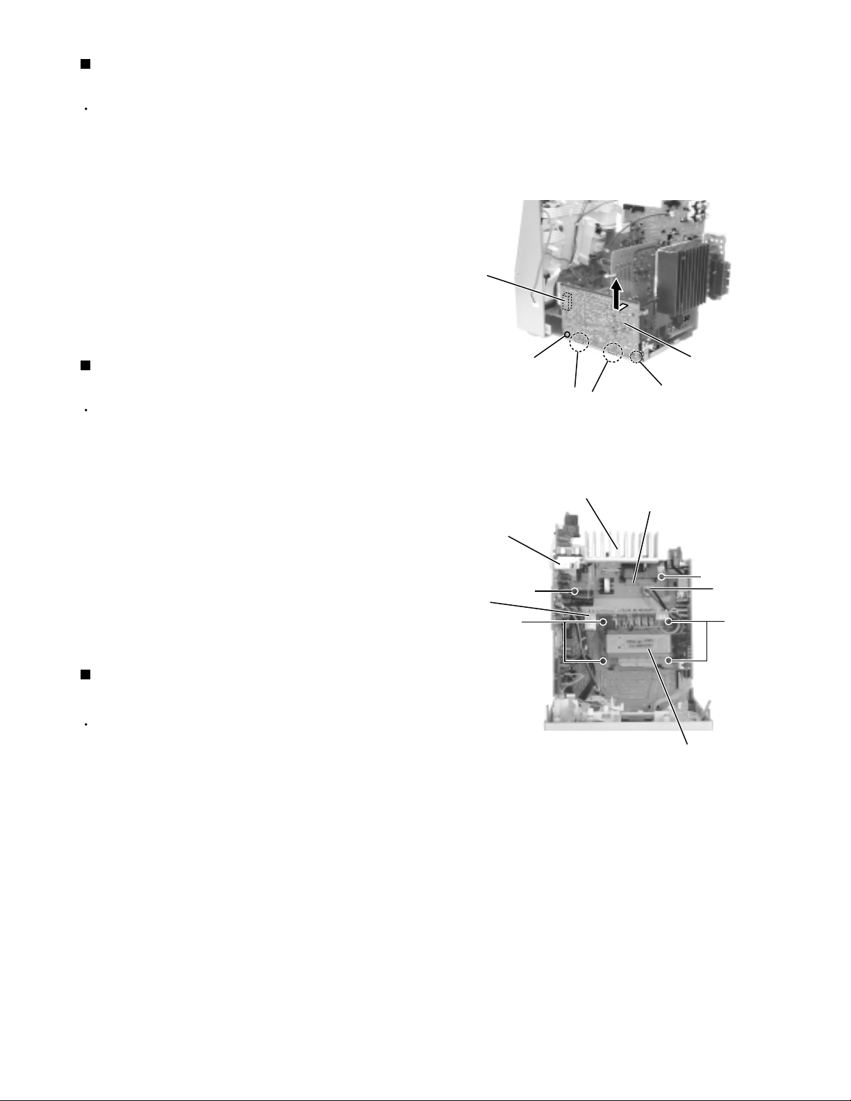
Page 8
UX-V30
<Cassette mechanism assembly>
Prior to performing the following procedure, remove
the rear cover, the side panels and the cassette
mechanism assembly.
Cassette door
Removing the Opt.Dig.out board
(See Fig.16)
1.
Remove the two screws K attaching the Opt.Dig.out
board on the side of the cassette mechanism
assembly.
Removing the cassette mechanism
assembly (See Fig.16 and 17)
Prior to performing the following procedure, remove
the Opt.Dig.out board.
1.
Press the eject button on the front side of the
cassette mechanism assembly to open the cassette
door.
2.
Remove the four screws L attaching the cassette
mechanism assembly on the back of the assembly.
Eject button
L
L
K
Opt, Dig.out board
Fig.16
Cassette mechanism
L
L
1-8
Fig.17
Page 9
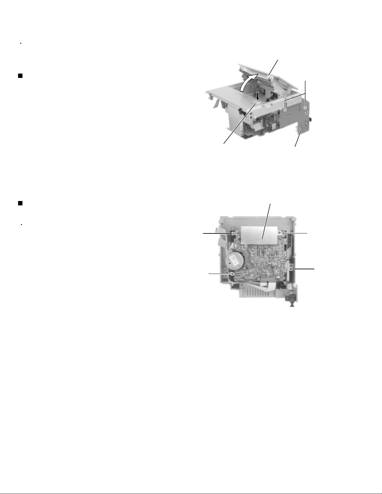
<Front panel assembly>
Prior to performing the following procedure, remove
the rear cover, the side panels, the cassette
mechanism assembly, the main board and the front
panel assembly.
M
UX-V30
CD mechanism cover
(CD mechanism assembly)
Removing the CD mechanism assembly
(See Fig.18 to 21)
1.
Disconnect the harness from connector CN721 and
CN722, and the card wire from CN766 on the LCD
board on the back of the front panel assembly.
2.
Remove the five screws M attaching the CD
mechanism cover to the front panel. Remove the CD
mechanism cover together with the CD mechanism
assembly.
3.
Release the harness from each hook on the CD
mechanism cover.
4.
Remove the five screws N attaching the CD
mechanism cover and the CD mechanism case.
Release the three joints g of the CD mechanism
cover and the CD mechanism case by pushing the
joint hooks inward.
5.
Disconnect the card wire from connector CN603 and
the harness from CN605 on the CD servo control
board.
6.
Remove the CD mechanism assembly from the CD
mechanism cover by pulling out it from the three
bosses h.
M
CN766
LCD board
Joint g
Fig.18
R
Belt
Loading motor
M
CN721
CN722
NN
CD mechanism cover
Loading motor
CD mechanism
case
N
Removing the LED board (A)
(See Fig.21)
1.
Remove the screw O attaching the LED board (A).
CD mechanism cover
CN603
CD servo control board
LCD board (A)
CN605
Joint g
Joint g
N
Fig.19
CD mechanism case
Joint g
CD mechanism cover
Fig.20Fig.21
1-9
Page 10
UX-V30
Removing the LED board (B) (See Fig.22)
Prior to performing the following procedure, remove
the CD mechanism assembly.
1.
Remove the screw P attaching the LED board (B).
Removing the CD door switch board
(See Fig.22)
1.
Release the hook i fixing the CD door switch board
to the CD mechanism cover.
Removing the CD servo control board
(See Fig.22)
Prior to performing the following procedure, remove
the CD mechanism assembly and the LED board (A)
/ (B).
1.
Remove the two screws Q attaching the CD servo
control board.
2.
Pull out the CD servo control board in the direction of
the arrow by releasing the two joints j.
Removing the loading motor
(See Fig.18)
1.
Remove the belt and the two screws R attaching the
loading motor on the back of the front panel
assembly.
CD door switch board
Hook i
P
LCD board (B)
M
M
CN766
LCD board
Operation switch board
Q
Q
Joint j
Fig.22
CD mechanism cover
(CD mechanism assembly)
CD servo control
board
R
Belt
Loading motor
M
CN721
Fig.18
CN722
S
O
LCD board (A)
Removing the LCD board assembly
(See Fig.23)
Prior to performing the following procedure, remove
the CD mechanism cover (CD mechanism
assembly).
1.
Remove the two screws S attaching the LCD board
assembly.
2.
Disconnect connector CN781 on the LCD board
assembly from the operation switch board.
Removing the operation switch board
(See Fig.24)
Prior to performing the following procedure, remove
the LCD board assembly.
1.
Remove the eight screws T attaching the operation
switch board.
1-10
CN781
T
T
LCD board assembly
Fig.23
Operation switch board
T
Fig.24
Page 11
UX-V30
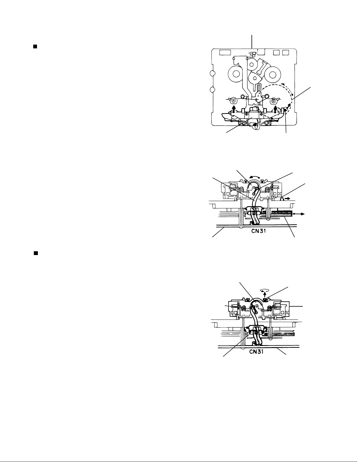
<<Cassette Mechanism Section>>
Removing the Playback/Recording & Eraser
Head ( See Figs. 1 and 2 )
1. While shifting the trigger arms seen on the right
side of the head mount in the arrow direction,
turn the flywheel R in counterclockwise direction
until the head mount has gone out with a click
(See Fig. 1).
2. When the flywheel R is rotated in counterclockwise
direction, the Playback/Recording & Eraser head
will be turned in counterclockwise direction from the
position in Fig. 2 to that in Fig. 3.
3. At this position, disconnect the flexible P.C. board
(outgoing from the Playback/Recording & Eraser head)
from the connector CN31 on the head amplifier &
mechanism control P.C. board.
4. After dismounting the FPC holder, remove the flexible
P.C. board.
5. Remove the flexible P.C. board from the chassis base.
6. Remove the spring Afro behind the Playback/Recording
& Eraser head.
7. Loosen the reversing azimuth screw retaining the Playback
/Recording & Eraser head.
8. Take out the Playback/Recording & Eraser head from the
front of the head mount.
9. The Playback/Recoring & Eraser head should also be
removed similarly according to Steps 1 ~ 8 above.
Frexible
board
Cassette mechanism
Fig. 1
Playback/Recording &
eraser hyead
Flywheel R
Trigger armHead mount
Spring "a"
Trigger arm
Reassembling the Playback/Recording & Eraser
Head
1. Reassemble the playback head from the front of the head
mount to the position as shown in Fig. 3.
2. Fix the reversing azimuth screw.
3. Set the spring "a" from behind the Playback/Recording &
Eraser head.
4. Attach the flexible P.C. board to the chassis base, and fix
it with the FPC holder as shown in Fig. 3.
5. The Playback/Recording & Eraser head should also be
reassembled similarly to Step 1 ~ 4 above.
Head amplifier & mechanism
control P.C. board
Fig. 2
Playback/Recording &
eraser head
Spring "a"
FPC holder
Fig. 3
Flywheel R
Reversing azimuth
screw
Head
mount
Frexible
board
Head amplifier &
mechanis control
P.C. board
1-11
Page 12

UX-V30
Removing the Head amplifier & Mechanism
control P.C. board
(See Fig. 4)
Belt
1. Remove the cassette mechanism assembly.
2. After turning over th cassette mechanism assembly,
remove the three screws "1" retaining the head
amplifier & mechanism control P.C. board.
3. Disconnect the connector CN32 on the P.C. board
including the connector CN 1 on the reel pulse P.C.
board.
4. When necessary, remove the 4 pin parallel wire
soldered to the main motor.
Removing the Main Motor Assembly
(See Fig. 4~6)
1. Remove the two screws "2" retaining the main
motor assembly (See Fig. 4, 4a).
2. While raising the main motor, remove the capstan
belt from the motor pulley (See Fig. 4a).
Caution 1: Be sure to handle the capstan belt so
carefully that this belt will not be
stained by grease and other foreign
matter. Moreover, this belt should be
hanged while referring to the capstan
belt hanging method in Fig. 5, 6.
Head amplifier &
mechanism control
P.C. board
Flexible P.C. board
Capstan belt
4pin parallel wire
Fig. 4
Main motor
assembly
Main motor
assembly
Main
moteor
assembly
Motor
pulley
Capstan
belt
1-12
Fig. 5
Mechanism motor
assembly
Motor
pulley
Fig. 4a
Main motor
assembly
Flywheel
Motor pulleyCapstan belt
Fig. 6
Page 13

Removing the Flywheel
(See Figs. 7 and 8)
1. Remove the head amplifier & mechanism control
P.C. board.
2. Remove the main motor assembly.
3. After turning over the cassette mechanism,
remove the slit washers "b" and "c" fixing the capstan
shafts R and L, and pull out the flywheel R and L
respectively from behind the cassette mechanism.
UX-V30
Flywheel R Flywheel L
Capstan shaft R Capstan shaft L
Flywheel R Flywheel L
Fig. 8
Removing the Reel Pulse P.C. board and Solenoid
(See Fig. 9)
1. Remove the five pails "d"~"h" reataining the reel pulse
P.C. board.
2. From the surface of the reel pulse P.C. board parts, remove
the two pawls "i" and "j" retaining the solenoid.
j
Solenoid
Slit
washer
Slit
washer
Fig.7
Reel pulse P.C. board
Fig. 9
1-13
Page 14

UX-V30
Main adjustment
Measurement Instruments Required for
Adjustment
1. Low frequency oscillator
This oscillator should have a capacity to output
0dBs to 600
50Hz-20kHz.
2. Attenuator impedance : 600
3. Electronic voltmeter
4. Distortion meter
5. Frequency counter
6. Wow & flutter meter
7. Test tape
VTT703L : Head azimuth
VT712 : Tape speed and running unevenness
(3kHz)
VT724 : Reference level (1kHz)
8. Blank tape
TYPE
TYPE
9. Torque gauge : For play and back tension
FWD(TW2111A), REV(TW2121a) and
FF/REW(TW2231A)
10. Test disc: CTS-1000
Measurement conditions
Power supply voltage
: AC230V (50Hz)----B/E/EE/EN
: AC110/127V/230V(50/60Hz)
: UB/UF/US/UX/U
Reference output : Speaker : 0.775V/4
: Headphone : 0.077V/32
Reference frequency and
input level ------------------------------ 1kHz, AUX : -8dBs
MIX MIC: -54dBs (UB/UF/US/UX/U)
Input for confirming recording and playback
characteristics ------------------------- AUX : -28dBs
Measurement output terminal ------- at Speaker J3002
Load resistance --------------------------- 4
Radio Input signal
AM frequency --------------------------------------- 400Hz
AM modulation ---------------------------------------- 30%
FM frequency --------------------------------------- 400Hz
FM frequency deviation ------------------------ 22.5kHz
at an oscillation frequency of
: AC-225
: AC-514
Tuner section
B/E/EN version
FM Band cover: 87.5
MW Band cover: 522
LW Band cover: 144
EE version
FM Band cover: 65
MW Band cover: 522
LW Band cover: 144
UB/UF/US/UX/U version
FM Band cover: 87.5
MW Band cover: 531
SW Band cover: SW1 2.3
: SW2 7
Voltage applied to tuner +B : DC5.7V
VT : DC 12V
Reference measurement
output 26.1mV(0.28V)/3
Input positions AM : Standard loop antenna
FM : TP1 (hot) and TP2 (GND)
Standard measurement position of volume
Function switch to Tape
Beat cut switch to Cut
Super Bass/Active hyper Bass to OFF
Bass Treble to Center
Adjustment of main volume to reference output
VOL : 28
Precautions for measurement
1. Apply 30pF and 33k
side and 0.082
sweeper input side.
2. The IF sweeper output level should be made as
low as possible within the adjustable range.
3. Since the IF sweeper is a fixed device, there is no
need to adjust this sweeper.
4. Since a ceramic oscillator is used, there is no need
to perform any MIX adjustment.
5. Since a fixed coil is used, there is no need to adjust
the FM tracking.
6. The input and output earth systems are separated.
In case of simultaneously measuring the voltage in
both of the input and output systems with an
electronic voltmeter for two channels, therefore, the
earth should be connected particularly carefully.
7. In the case of BTL connection amp., the minus
terminal of speaker is not for earthing. Therefore, be
sure not to connect any other earth terminal to this
terminal. This system is of an BTL system.
8. For connecting a dummy resistor when measuring
the output, use the wire with a greater code size.
9. Whenever any mixed tape is used, use the band
pass filter (DV-12).
F and 100k in series to the
108MHz
1,629kHz
288kHz
74MHz, 87.5 108MHz
1,629kHz
288kHz
108MHz
1,602kHz, 530 1,710kHz
6.995MHz
21.85MHz
to the IF sweeper output
1-14
Page 15

<<
Arrangement of Adjusting Position
UX-V30
>>
Cassette mechanism section
Head azimuth
adjusting screw
(Forward side)
Head azimuth
adjusting screw
(Reverse side)
Cassette mechanism section (Back side)
Head azimuth
adjusting screw
(Forward side)
Playback/Recording &
eraser head
Head azimuth
adjusting screw
(Reverse side)
Front panel assembly section
VR201
R ch BIAS ADJ
VR101
L ch BIAS ADJ
L301
MOTOR SPEED
VR301
1-15
Page 16

UX-V30
Tape Recorder Section
Items
Confirmation
of head angle
Measurement
conditions
Test tape
: VTT703L (8kHz)
Measurement output
terminal
: Speaker terminal
Speaker R
(Load resistance: 4 )
: Headphone terminal
Measurement method
1 Playback the test tape VTT703L (8kHz)
2 With the recording & playback mechanism,
adjust the head azimuth screw so that the
forward and reverse output levels become
maximum. After adjustment, lock the head
azimuth at least by half turn.
3 In either case, this adjustment should be
performed in both the forward and reverse
directions with the head azimuth screw.
Confirmation
of tape speed
Test tape
: VT712 (3kHz)
Measurement output
terminal
: Headphone terminal
Adjust VR37 so that the frequency counter
reading becomes 2,940~3,090Hz when
playing back the test tape VT712 (3kHz) with
playback and recording mechanism after
ending forward winding of the tape.
Reference Values for Confirmation Items
Standard
Values
Maximum
output
Tape speed
of deck
: 2,940 ~
3,090Hz
Adjusting
positions
Adjust the head
azimuth screw
only when the
head has been
changed.
VR301
Items
Difference
between the
forward and
reverse speed
Measurement
conditions
Test tape
: VT712 (3kHz)
Measurement output
terminal
: Speaker terminal
Speaker R
(Load resistance: 4 )
Measurement output
terminal
: Headphone
Wow & flutter Test tape
: VT712 (3kHz)
Measurement output
terminal
: Headphone terminal
Measurement method
Standard
Values
When the test tape VT712 (3kHz) has been
played back with the recording and playback
mechanism at the beginning of forward
winding, the frequency counter reading of the
difference between both of the mechanism
should be 6.0Hz or less.
When the test tape VT712 (3kHz) has been
played back with the recording and playback
mechanism at the beginning of forward
winding, the frequency counter reading of
wow & flutter should be 0.25% or less
(WRMS).
6.0Hz or
less
0.25% or
less
(WRMS)
Adjusting
positions
Head azimuth
screw
1-16
Page 17

Electrical Performance
UX-V30
Items
Adjustment of
recording bias
current
(Reference
Value)
Adjustment of
recording and
playback
frequency
characteristics
Measurement
conditions
Mode: Forward or
reverse mode
Recording mode
Test tape
: AC-514 to TYPE
and AC-225 to
TYPE
Measurement output
terminal
: Both recording and
headphone terminals
Reference frequency
: 1kHz and 10kHz
(REF.: -20dB)
Test tape
: AC-514 to TYPE
Measurement input
terminal
: OSC IN
Measurement method
Standard
Values
1 With the recording and playback
mechanism, load the test tapes (AC-514 to
TYPE
and AC-225 to TYPE ), and set
the mechanism to the recording and
pausing condition in advance.
2 After connecting 100
in series to the
recorder head, measure the bias current
with a valve voltmeter at both of the
terminals.
3 After resetting the [PAUSE] mode, start
recording. At this time, adjust VR31 for Lch
and VR32 for Rch so that the recording
bias current values become 4.0
) and 4.20 A (TYPE ).
A (TYPE
1 With the recording and playback
mechanism, load the test tapes (AC-514 to
TYPE
), and set the mechanism to the
recording and pausing condition in
advance.
2 While repetitively inputting the reference
frequency signal of 1kHz and 10kHz from
OSC IN, record and playback the rape.
3 While recording and playback the test tape
in TYPE
, adjust VR31 for Lch and VR32
for Rch so that the output deviation
between 1kHz and 10kHz becomes
-1dB
2dB.
AC-225
: 4.20
AC-514
: 4.0
Output
deviation
between
1kHz and
10kHz
: -1dB
Adjusting
positions
L ch
: VR101
A
R ch
: VR201
A
L ch
: VR101
R ch
: VR201
2dB
Reference Values for Electrical Function Confirmation Items
Items
Recording
bias
frequency
Measurement
conditions
Forward or reverse
Test tape
: TYPE
(AC-514)
Measurement
terminal : BIAS TP on
P.C. board
Measurement method
1 While changing over to and from BIAS 1
and 2, confirm that the frequency is
changed.
2 With the recording and playback
mechanism, load the test tape.
(AC-514 to TYPE
), and set the
mechanism to the recording and pausing
condition in advance.
3 Confirm that the BIAS TP frequency on the
P.C. board is 100kHz
Eraser
current
(Reference
value)
Forward or reverse
Recording mode
Test tape
: AC-514 to TYPE
and AC-225 to
TYPE
Measurement
terminal : Both of the
eraser head terminals
1 While recording and playback mechanism,
load the test tapes (AC-514 to TYPE
and AC-225 to TYPE ), and set the
mechanism to the recording and pausing
conditions in advance.
2 After setting to the recording conditions,
connect 1W in series to the eraser head on
the recording and playback mechanism
side, and measure the eraser current from
both of the eraser terminals.
6kHz.
Standard
Values
100 kHz
6 kHz
TYPE
: 120 mA
TYPE
: 75 mA
Adjusting
positions
1-17
Page 18

UX-V30
Flow of functional operation until TOC read
Power ON
Power Key
Slider turns REST
SW ON.
Automatic tuning
of TE offset
Check Point
Check that the voltage at the pin17
of CN604 is 0V (a moment)?
VREF
Tracking error waveform at TOC reading
pin 25 of
IC601(TE)
Approx
1.8V
Tracking
servo
Disc statas
to rotate
off statas
Automatic measurement
of TE amplitude and
automatic tuning of
TE balance
Approx.3sec
Tracking
servo
on statas
Disc to be
braked to stop
TOC reading
finishes
500mv/div
2ms/div
Fig.1
Laser ON
Detection of disc
Automatic tuning of
Foucus offset
Automatic measurement of
Focus A-curve amplitude
Disc is rotated
Focus servo ON
(Tracking servo ON)
Automatic measurement of
Tracking error amplitude
Automatic tuning of
Tracking error balance
Check that the voltage at the
pin3 of IC601 + side is + 5V?
Confirm that the Focus error
S-cuve siganl at the pin27 of
IC601 is approx.2Vp-p
Confirm that the siganl from
pin24 IC603 is 0V as a
accelerated pulse during
approx.400ms.
Confirm the waveform of
the Tracking error signal
at the pin25 of IC601 (R612)
(See fig-1)
1-18
Automatic tuning of
Focus error balance
Automatic tuning of
Focus error gain
Automatic tuning of
Tracking error gain
TOC reading
Play a disc
Confirm the eys-pattern
at the lead of TP1
Page 19

UX-V30
Turn off the power switch and,disconnect the
power cord from the ac outlet.
Replace the pickup with a normal one.(Refer
to
Pickup Removal on the previous page)
Plug the power cord in,and turn the power on.
At this time,check that the laser emits for
about 3seconds and the objective lens moves
up and down.
Note: Do not observe the laser beam directly.
Play a disc.
Check the eye-pattern at TP1.
Finish.
Maintenance of laser pickup
(1) Cleaning the pick up lens
Befor you replace the pick up, please try to
clean the lens with a alcohol soaked cotton
swab.
(2) Life of the laser diode (Fig.1)
When the life of the laser diode has expired,
the following symptoms wil appear.
(1) The level of RF output (EFM output:ampli
tude of eye pattern) will below.
Is RF output
1.1 0.15Vp-p?
Replace it.
NO
YES
O.K
(3) Semi-fixed resistor on the APC PC board
The semi-fixed resistor on the APC printed
circuit board which is attached to the pickup
is used to adjust the laser power.Since this
adjustment should be performed to match the
characteristics of the whole optical block,
do not touch the semi-fixed resistor.
If the laser power is lower than the specified
value,the laser diode is almost worn out, and
the laser pickup should be replaced.
If the semi-fixed resistor is adjusted while
the pickup is functioning normally,the laser
pickup may be damaged due to excessive current.
(Fig.1)
Replacement of laser pickup
1-19
Page 20

UX-V30
Description of major ICs
LA6541-X(IC541) : Servo Driver
1. Pin Layout & Block Diagram
Vcc Vref Vin4 Vg4 Vo8 Vo7
24 23
22
20
21
19
11k
Vcc
Gnd
Vo6 Vo5 Vg3 Vin3 Cd Res
18
17 16
ohm
- +
- +
Level
shift
Level
shift
B T L
driver
B T L
driver
B T L
driver
B T L
driver
Level
shift
Level
shift
11k
ohm
1
2
Vcc Mute Vin1 Vg1 Vo1 Vo2 Vo3 Vo4 Vg2 Vin2 Reg
3456
Gnd
7 8 9101112
2. Pin functions
Pin
Symbol Function
No.
1
10
11
12
13
14
15
16
17
18
19
20
21
22
23
24
2
3
4
5
6
7
8
9
Vcc
Mute
Vin1
Vg1
Vo1
Vo2
Vo3
Vo4
Vg2
Vin2
Reg Out
Reg In
Res
Cd
Vin3
Vg3
Vo5
Vo6
Vo7
Vo8
Vg4
Vin4
Vref
Vcc
Power supply (Shorted to pin 24)
All BTL amplifier outputs ON/OFF
BTL AMP 1 input pin
BTL AMP 1 input pin (For gain adjustment)
BTL AMP 1 input pin (Non inverting side)
BTL AMP 1 input pin (Inverting side)
BTL AMP 2 input pin (Inverting side)
BTL AMP 2 input pin (Non inverting side)
BTL AMP 2 input pin (For gain adjustment)
BTL AMP 2 input pin
External transistor collector (PNP) connection. 5V power supply output
External transistor (PNP) base connection
Reset output
Reset output delay time setting (Capacitor connected externally)
BTL AMP 3 input pin
BTL AMP 3 input pin (For gain adjustment)
BTL AMP 3 output pin (Non inverting side)
BTL AMP 3 output pin (Inverting side)
BTL AMP 4 output pin (Inverting side)
BTL AMP 4 output pin (Non inverting side)
BTL AMP 4 output pin (For gain adjustment)
BTL AMP 4 output pin
Level shift circuit's reference voltage application
Power supply (Shorted to pin 1)
15
14
13
11k
ohm
RESET
Regulator
11k
ohm
Reg
out
In
1-20
Page 21

MN35510 (IC651) : DIGITAL SERVO&DIGITAL SIGNAL PROCESSER
UX-V30
1. Terminal Layout
2.Block Diagram
LRCKIN(MSEL)
BCLK(SSEL)
SRDATAIN
(PSEL)
IOSEL
CLVS
CRC
BLKCK
CLDCK
SBCK
SUBC
DEMPH
RESY
FLAG6(RESY)
SSEL
SQCK
SUBQ
AVDD2
AVDD2
PCK
EFM
PLLF
DSLF
IREF
DRF
ARF
RSEL
PSEL
MLD
MCLK
MDATA
CK384(EFM)
VCOF
BYTCK
SMCK
FCLK
CSEL
MSEL
X2
X1
ÊSTAT
DIGITAL
DEEMPHSIS
SUB
CODE
BUFFER
DSL.
PLL
VCO
VCO
ITUNING
GENERATION
PITCH
CONTROL
20 ~ 1
21
~
40
41 ~ 60
8TIMES
OVER SAMPUNC
DIGITAL FILTER
EFM
DEMODULATION
SYNC
INTERPOLATION
SUBCODE
DEMODULATION
MICRO
COMPUTER
INTERFACE
A/D
COVERTER
80
~
61
1BIT
DAC
LOGIC
S
16k
SRAM
CIRC
ERROR
CORRECTION
DEINTERLEVE
CLV
SERVO
INPUT
PEM
(R)
PEM
(L)
D/A
CONVERTER
OUTPUT
DIGITAL
AUDIO
INTERFASE
DIGITAL
AUDIO
INTERFASE
INTER POLATION
SOFT MUTING DIGITAL
ATTENUATION
PEAK DETECTIVE
AUTO CUE
PORT
SERVO
TIMING GENERATOR
AVSS1
AVDD1
OUTR
OUTL
FLAG
IPFLAG
TX
ECM
PC
LRCK
SRDATA
BCLK
DMUTE
TRKV
KICK
VREF
TRVSTR
ECS
TVD
TRD
FOD
TBAL
FBAL
TOFS
TES
/TLOCK
/FLOCK
PLAY
LDON
WVEL
SENSE
D
/
D
V
V
V
S
D
D
S
D
D
1
/
R
V
T
S
S
E
T
S
S
1
T
F
E
R
T
F
E
E
N
V
T
R
C
R
S
B
V
D
D
O
E
T
/
R
F
D
E
O
F
T
1-21
Page 22

UX-V30
3. Description
Pin
symbol
No.
BCLK
1
2
LRCK
SRDATA
3
4
DVDD1
DVSS1
5
6
TX
7
MCLK
8
MDATA
9
MLD
10
SENSE
11
FLOCK
12
TLOCK
13
BLKCK
14
SQCK
15
SUBQ
16
DMUTE
STATUS
17
18
RST
19
SMCK
20
PMCK
21
TRV
22
TVD
23
PC
24
ECM
25
ECS
26
KICK
TRD
27
28
FOD
29
VREF
30
FBAL
31
TBAL
FE
32
TE
33
34
RF ENV
35
VDET
OFT
36
37
TRCRS
38
RFDET
BDO
39
LDON
40
I/O
O
Not used
Not used
O
O
Not used
I
Power supply (Digital)
I
Connected to GND
Digital audio interface output
O
com command clock signal input
I
(Data is latched at signal's rising point)
com command data input
I
I
com command load signal input
Sence signal output
O
O
Focus lock signal output Active :Low
O
Tracking lock signal output Active :Low
sub-code
O
I
Outside clock for sub-code Q resister input
Sub-code Q -code output
O
I
Connected to GND
Status signal
O
(CRC,CUE,CLVS,TTSTOP,ECLV,SQOK)
Reset signal input (L:Reset)
I
I
Not used
I
Not used
O
Traverse enforced output
O
Traverse drive output
I
Not used
Spindle motor drive signal (Enforced
O
mode output) 3-State
Spindle motor drive signal (Servo error
O
signal output)
Kick pulse output
O
Tracking drive output
O
O
Focus drive output
Reference voltage input pin for D/A
I
output block (TVD,FOD,FBA,TBAL)
Focus Balance adjust signal output
O
O
Tracking Balance adjust signal output
Focus error signal input(Analog input)
I
Tracking error signal input(Analog input)
I
I
RF envelope signal input(Analog input)
Vibration detect signal input(H:detect)
I
Off track signal input(H:off track)
I
Track cross signal input
I
RF detect signal input(L:detect)
I
BDO input pin(L:detect)
I
Laser ON signal output(H:on)
O
Description
block clock signal output
Pin
No.
41
42
43
44
45
46
47
48
49
50
51
52
53
54
55
56
57
58
59
60
61
62
63
64
65
66
67
68
69
70
71
72
73
74
75
76
77
78
79
80
symbol
TES
PLAY
WVEL
ARF
IREF
DRF
DSLF
PLLF
VCOF
AVDD2
AVSS2
EFM
PCK
PDO
SUBC
SBCK
VSS
XI
X2
VDD
BYTCK
CLDCK
FLAG
IPPLAG
FLAG
CLVS
CRC
DEMPH
RESY
IOSEL
TEST
AVDD1
OUT L
AVSS1
OUT R
RSEL
CSEL
PSEL
MSEL
SSEL
I/O
Tracking error shunt signal output(H:shunt)
O
I
Not used
I
Not used
I
RF signal input
Reference current input pin
I
Bias pin for DSL
I
I/O
Loop filter pin for DSL
Loop filter pin for PLL
I/O
I
Not used
I
Power supply(Analog)
Connected to GND(Analog)
Not used
III
Not used
I
Not used
I
Not used
I
Not used
Connected to GND(for X'tal oscillation
I
circuit)
Input of 16.9344MHz X'tal oscillation circuit
I
Output of X'tal oscillation circuit
O
I
Power supply(for X'tal cscillation circuit)
I
Not used
I
Not used
I
Not used
I
Not used
I
Not used
I
Not used
I
Not used
Not used
I
Not used
III
pull up
pull up
Power supply(Digital)
Lch audio output
O
I
Connected to GND
Rch audio output
O
II
pull up
Connected to GND
I
Connected to GND
I
Connected to GND
I
Pull up
Description
1-22
Page 23

AN8806SB-W(IC301) :RF&SERVO AMP
1.Pin layout
UX-V30
PD 1
LD 2
LDON 3
LDP 4
VCC 5
RF- 6
RF OUT 7
RF IN 8
C.AGC 9
ARF 10
C.ENV 11
C.EA 12
CS BDO 13
BDO 14
CS BRT 15
OFTR 16
/NRFDET 17
GND 18
2.Block diagram
36 PDAC
35 PDBD
34 PDF
33 PDE
32 PDER
31 PDFR
30 TBAL
29 FBAL
28 EF27 EF OUT
26 TE25 TE OUT
24 CROSS
23 TE BPF
22 VDET
21 LD OFF
20 VREF
19 ENV
6
29
728
27
910 17
8
11
12 19
+
- +
+
EQ
AGC
RF
DET
ENV CURCUIT
36
+
35
+
31
34
-
+
VCBA
-
+
VCBA
-
-
VCBA
+
+
OFTR
BDO
+
13
14
15
16
20
+
- +
32
33
+
-
VCBA
+
+ -
+
- +
21
2
+
-
24 25
30
23
26
22
14
3
1-23
Page 24

UX-V30
3. Pin function
Pin No.
1
2
3
4
5
6
7
8
9
10
11
12
13
14
15
16
17
18
19
20
21
22
23
24
25
26
27
28
29
30
31
32
33
34
35
36
symbol
PD
LD
LD ON
LDP
VCC
RF-
RF OUT
RF IN
C.AGC
ARF
C.ENV
C.EA
CS BDO
BDO
CS BRT
OFTR
/NRFDET
GND
ENV
VREF
LD OFF
VDET
TE BPF
CROSS
TE OUT
TE-
FE OUT
FEFBAL
TBAL
PDFR
PDER
PDF
PDE
PD BD
PD AC
I/O
I
APC amp . Input terminal
APC amp . Output terminal
O
LD ON/OFF control terminal
I
Connect to GND
-Power supply
-RF amp . Reversing input terminal
I
RFamp . Output terminal
O
AGC input terminal
I
AGC loop filter connection terminal
I/O
ARF output terminal
O
RF detection capacity connection terminal
I/O
HPF-amp capacity connection terminal
I/O
Capacity connection terminal for RF discernment side envelope detection
I/O
BDO output terminal
O
Capacity connection terminal for RF discernment side envelope detection
I/O
O
OFTR output terminal
RFDET output terminal
O
--
Connect to GND
O
3TENV output terminal
O
VREF output terminal
--
APC OFF control terminal
O
VDET output terminal
I
VDET input terminal
O
CROSS output terminal
O
TE amp . Output terminal
I
FE amp . Reversing input terminal
O
FE amp . output terminal
I
FE amp . Reversing input terminal
I
F.BAL control terminal
I
T.BAL control terminal
I/O
I-V amp conversion resistance adjustment terminal
I/O
I-V amp conversion resistance adjustment terminal
I
I-V amp input terminal
I-V amp input terminal
I
I
I-V amp input terminal
I
I-V amp input terminal
Function
1-24
Page 25

UPD78064GF-108 (IC701): System CPU
1.Pin layout
2.Pin function
31 ~ 50
100 ~ 81
80
51
1
30
Pin
No.
Symbol
I/O
Function
Pin
No.
Symbol
I/O
Function
1
2
3
4
5
6
7
8
9
10
11
12
13
14
15
16
17
18
19
20
21
22
23
24
25
26
27
28
I/O
O
I
O
-
I
I
I
I
I
O
O
O
O
O
O
O
O
O
I
O
I
Serial data
Serial clock
CD Q code data
Non connect
CD Q code data synchronizing clock
Connected to VSS
Main system clock
Main system clock
Power supply
Sub system clock
Sub system clock
Reset
Remote control
Non connect
Jog encoder 1
Main clock selection 2
Main clock selection 1
Switched 5V control
CD LSI reset
CD LSI command clock
CD LSI command data
CD LSI command load
Tape playback mute
Tape IC strobe
Tape end detection
Function AUX
AD converter GND
CD abnormal voltage detection
USDATA
USCK
UQRIN
UNC
USQCK
ICVSS
UX2
UX1
VDD
UXT1
UXT2
URESET
UREM
URDSCK
UJOG1
UBEAT2
UBEAT1
U+BCTL
UXRESET
UMCLK
UMDATA
UMLD
UPBMUTE
ULATCH
UREEL
UFAUX
UAVSS
USAFEYCD
29
30
31
32
33
34
35
36
37
38
39
40
41
42
43
44
45
46
47
48
49
50
I
I
I
I
I
I
I
-
I
O
I
O
I
O
O
O
O
O
O
O
O
-
-
O
I
[RESET/CLOSE] switch
Abnormal voltage detection 1
Abnormal voltage detection 2
Body key input 1
Body key input 0
Tape switch 0
Tape switch 1
AD converter power supply
AD converter reference voltage
Backup power supply decision
Function tuner
GND
FM stereo detection
Tuner PLL strobe
JOG encoder 2
BASS control
TRE control
VOL.control
AHB on/off
System muting
Power ON/OFF
Function CD
LCD common
LCD bias voltage
LCD bias voltage
GND
LCD segment
LCD LSI status
URESET/CLOSE
USAFETY1
USAFETY0
UKEY1
UKEY0
UTAPE0
UTAPE1
AVDD
UAVREF
UBUP
UFTUNER
VSS
UMPX
UPERIOD
UJOGB
UBASS
UTRE
UVOL
USBASS
USMUTE
UPOUT
UFCD
COM0~3
BIAS
VLC0~2
VSS
S0~39
USTATUS
51~54
56~58
60~99
55
59
100
~
~
UX-V30
1-25
Page 26

UX-V30
LA1838(IC102): FM AM IF AMP&detector, FM MPX Decoder
1. Block Diagram
30
ALC
BUFF
FM
S-METER
FM IF
1
2. Pin Function
Pin
Symbol
No.
FM IN
1
AM MIX
2
3
FM IF
AM IF
4
GND
5
6
TUNED
STEREO
7
8
VCC
9
FM DET
10
AM SD
FM VSM
11
AM VSM
12
13
MUTE
14
FM/AM
MONO/ST O
15
29
28
AM
OSC
SD
COMP
S-CLRVE
PM
DET
2
I/O
I
This is an input terminal of FM IF
REG
AM
MIX
AM/FM
IF-BUFF
3
27
FM
RF.AMP
AM IF
4
26
AGC
AM
S-METER
GND
Function
DET
5
signal.
This is an out put terminal for AM
O
mixer.
I
Bypass of FM IF
Input of AM IF Signal.
I
I
This is the device ground terminal.
When the set is tunning,this terminal
O
becomes "L".
O
Stereo indicator output. Stereo "L",
Mono: "H"
III
This is the power supply terminal.
I
FM detect transformer.
I
This is a terminal of AM ceramic filter.
O
Adjust FM SD sensitivity.
O
Adjust AM SD sensitivity.
I/O
When the signal of IF REQ of IC121(
LC72131) appear, the signal of FM/AM
IF output. //Muting control input.
Change over the FM/AM input.
I
"H" :FM, "L" : AM
Stereo : "H", Mono: "L"
25
TUNING
DRIVE
6
24
STEREO
DRIVE
7
22
23
P-DET
VCC
89
Pin
Symbol
No.
16
R OUT
17
L OUT
18
19
20
21
22
23
24
25
26
27
28
29
30
R IN
L IN
RO
LO
IF IN
FM OUT
AM DET
AM AGC
AFC
AM RF
REG
AM OSC
OSC BUFFER
21
DECODER
ANIT-BIRDIE
VCO
384KHz
10
20
STEREO
5N
SW
FF
38k
11
I/O
O
Right channel signal output.
O
Left channel signal output.
Input terminal of the Right channel post
I
18
19
MUTE
FF
/
19k
2
12 13
FF
19k
/
LS
Function
17 16
PILOT
DET
14
AMP.
Input terminal of the Left channel
I
post AMP.
Mpx Right channel signal output.
O
O
Mpx Left channel signal output.
I
Mpx input terminal
FM detection output.
O
AM detection output.
O
This is an AGC voltage input terminal
I
for AM
I
This is an output terminal of voltage
for FM-AFC.
AM RF signal input.
I
Register value between pin 26 and pin28
O
besides the frequency width of the
input signal.
I
This is a terminal of AM Local
oscillation circuit.
AM Local oscillation Signal output.
O
15
1-26
Page 27

LC72136N (IC121) : PLL Frequency Synthesizer
1. Pin layout
FM/AM
CLOCK
FM/ST/VCO
AM/FM
2. Block diagram
XT
CE
DI
DO
SDIN
1
2
3
4
5
6
7
8
9
10
11
22
21
20
19
18
17
16
15
14
13
12
XT
GND
LPFOUT
LPFIN
PD
VCC
FMIN
AMIN
IFCONT
IFIN
UX-V30
1
22
16
15
3
4
5
6
17
21
3. Pin function
Pin
Symbol
No.
1
2
3
4
5
6
7
8
9
10
11
XT
FM/AM
CE
DI
CLOCK
DO
FM/ST/VCO
AM/FM
LW
MW
SDIN
Reference
Driver
Swallow Counter
1/2
C
2
B
I/F
Power
on
Reset
Function
I/O
X'tal oscillator connect (75kHz)
I
LOW:FM mode
O
When data output/input for 4pin(input) and
I
Swallow Counter
1/16,1/17 4bit
1/16,1/17 4bit
12bit
Programmable
DriverS
Data Shift Register & Latch
7821113
6pin(output): H
Input for receive the serial data from
I
controller
Sync signal input use
I
Data output for Controller
O
Output port
"Low": MW mode
O
Open state after the power on reset
O
Input/output port
I/O
Input/output port
I/O
Data input/output
I/O
Phase
Detector
Charge Pump
Unlock
Detector
Universal
Counter
Pin
No.
12
IFCONT
13
14
15
16
17
18
19
LPFOUT
20
21
22
Symbol
IFIN
AMIN
FMIN
VCC
PD
LPFIN
GND
XT
18
19
20
12
I/O
Function
IF counter signal input
I
IF signal output
O
Not use
-
AM Local OSC signal output
I
FM Local OSC signal input
I
Power suplly(VDD=4.5-5.5V)
When power ON:Reset circuit move
PLL charge pump output(H: Local OSC
O
frequency Height than Reference frequency.
L: Low Agreement: Height impedance)
Input for active lowpassfilter of PLL
I
Output for active lowpassfilter of PLL
O
Connected to GND
X'tal oscillator(75KHz)
I
1-27
Page 28

UX-V30
BA15218N (IC342/IC343/IC391/IC453IC362/IC363)
: Dual Ope. Amp.
+
+
1
-
1 2 3 4 5 6 7 8
OUT1 +IN1 +IN1
+IN2 -IN2 OUT2
GND
2
-
Vcc
BU4094BCF-X(IC304,IC303):Serial to parallel port extension
1.Pin layout
STROBE
DATA
CLOCK
Q1
Q2
Q3
Q4
Vss
2.Block diagram
1
2
3
4
5
6
7
8
16
Vdd
15
OUTPUT ENABLE
14
Q5
13
Q6
12
Q7
11
Q8
10
Q's
9
Qs
DA TA
CLOCK
STROBE
OUTPUT
ENABLE
15
2
8-STAGE
3
1
SHIFT REGISTER
8-BIT
10
9
Q's
Qs
SERIAL
OUTPUT
LATHES
3-STATE
OUTPUTS
Q1
Q8
PARALLEL OUTPUT
1-28
Page 29

GP1U271X (IC701) : Receiver for remote
+
–
Amp.
Limiter Integrator Comparator
LB1641 (IC501) : DC Motor Driver
1. Pin Layout
B.P.F
Demodulator
GND
UX-V30
VCC Vout
1 2 3 4 5 6 7 8 9
GNDOUT1 P1
VZ IN1 IN2
2. Pin Functions
Input Output
IN1 IN2 OUT1 OUT2
0 0 0 0
1 0 1 0
0 1 0 1
1 1 0 0
VCC1
10
VCC2 P2
OUT2
Mode
Brake
CLOCKWISE
COUNTER-CLOCKWISE
Brake
1-29
Page 30

UX-V30
AN7345(IC302) PB/REC AMP
1
2. Pin Function
Pin
Symbol
No.
1
R1
2
R2
L1
L2
NF1
24
1
R1
I/O
I
Playback amplifier input
Playback amplifier input
I
R2
23
2
22
3
NF2
AMP
AMP
Pre
Pre
OUT1
4
OUT2
Function
EQ1
2021
EQ
CTRL
5
EQ2
CTL1
Pre
Source
CTRL
6
CTL2
RIN1
RNF1
1819
17
78
RIN2
RNF2
Pin
No.
13
14
9
EQ
CTL
ALC
10 11
LC
I/O
I
I
VCC
RF
141516
13
REPPLE
REJ
12
LPF GND
Repple filter
ROUT1
ALC
AMP
ALC
AMP
ROUT2
Symbol
Vcc Power supply
RF
Function
3
NF2
4
OUT2 Playback amplifier output
EQ2 I
5
CTL2 I Pre Amplifier input swithing time
6
RIN2 I
7
RNF2 I Recording amplifier negative feedback
8
ROUT2
9
LC I
10
11
LPF
GND I
12
I
Playback amplifier negative feedback
O
Equlaizer
constant
Recording amplifier input
Recording amplifier output
O
ALC low cut
ALC low pass filter
I
EQCTL EQ control
15
16
ROUT
17
RNF1 Recording amplifier negative feedback
RIN1
18
CTL1
19
20
EQ1 Equlayzer
21
OUT1
NF1
22
L2 I
23
24
L1
I
O
Recording amplifier output
I
I Recording amplifier input
Pre amplifier input swithing control
I
I
Playback amplifier output
O
Playback amplifier negative feedback
I
Playback amplifier input
Playback amplifier input
I
1-30
Page 31

LC75342
UX-V30
1-31
Page 32

UX-V30
3. Pin function
Pin No.
1
2
3
4
5
6
7
8
9
10
11
12
13
14
15
16
17
18
19
20
21
22
23
24
25
26
27
28
29
30
symbol
D1
CE
Vss Ground
TEST
LOUT Volume+equalizer output
LBASS2
LBASS1
LTRE
LIN
LSEL0 Input selector output pin
L4
L3
L2
L1
NC
NC
R1
R2
R3
R4
RSEL0
RIN
RTRE
RBASS1
RBASS2
ROUT
NC
Vref
VDD
CL Clock input
I/O
Serial data input pin for control
I
Chip enable pin
I
-I
TEST pin for electronic volume control
O
Bas-band filter comprising capacitor and resistor connection
O
Bas-band filter comprising capacitor and resistor connection
I
Capacitor connection pin comprising treble band filter
I
Volume+equalizer intput
I
O
Input signal pin
I
Input signal pin
I
Input signal pin
I
I
Input signal pin
--
No connect
--
No connect
Input signal pin
I
Input signal pin
I
Input signal pin
I
Input signal pin
I
Input selector output pin
O
I
Volume+equalizer intput
I
Capacitor connection pin comprising treble band filter
I
Bas-band filter comprising capacitor and resistor connection
Bas-band filter comprising capacitor and resistor connection
O
O
Volume+equalizer output
-- No connect
Analog ground
O
I
Poer Supply
I
Function
1-32
Page 33

LC72723
1.
Pin Assignment
Block diagram
2.
VREF
FLOUT
UX-V30
CIN
Vdda
REFERENCE
VOLTAGE
Vssa
MPXIN
TEST
3. Pin functions
Pin
Symbol
No.
1
VREF
2
MPXIN
Vdda
3
4
Vssa
5
FLOUT
6
CIN
TEST
7
8
XOUT
9
XIN
10
Vssd
11
Vddd
12
MODE
13
RST
14
RDDA
RDCL
15
16
RDS-ID
READY
ANTIALIASING
FILTER
TEST
I/O
O
I
O
I
I
O
I
I
I
O
I/O
O
CLOCK
RECOVERY
(1187.5kHz)
DECODER
(128-bits)
RDS-ID
DETECT
57kHz
BPF
(SCF)
SMOOTHING
FILTER
CLK(4.332MHz)
OSC
XIN
PLL
(57kHz)
VREF
XDUT
Function
Reference voltage output (Vdda/2)
Baseband (multiplexed) signal input
Analog power supply (+5V)
Analog ground
Subcarrier input (filter output)
Subcarrier input (comparator input)
Test input
Crystal oscillator output (4.332MHz)
Crystal oscillator input (exeternal reference input)
Digtal ground
Digtal power supply
Read mode setting (0:master,1:slave)
RDS-ID/RAM reset (positive polarity)
RDS data output
RDS clock output (master mode)/RDS clock input (slave mode)
RDS-ID/READY output (negative polarity)
DATA
RAM
Vddd
Vssd
RDDA
RDCL
MDDE
RST
RDS-ID/
READY
1-33
Page 34

UX-V30
<<MEMO>>
1-34
Page 35

UX-V30
UX-V30
VICTOR COMPANY OF JAPAN, LIMITED
AUDIO & COMMUNICATION BUSINESS DIVISION
PERSONAL & MOBILE NETWORK BUSINESS UNIT 10-1,1Chome,Ohwatari-machi,Maebashi-city,371-8543,Japan
No.20888
Printed in Japan
200012(O)
1-35
 Loading...