

Page 1
SERVICE MANUAL
COMPACT COMPONENT SYSTEM
MB725<Rev.001>20103SERVICE MANUAL
UX-TB30B, UX-TB30E, UX-TB30EN,
UX-TB30EV
XT-UXTB30
AX-UXTB30
COPYRIGHT © 2010 Victor Company of Japan, Limited
Lead free solder used in the board (material : Sn-Ag-Cu, melting point : 219 Centigrade)
SP-UXTB30SP-UXTB30
TABLE OF CONTENTS
1 PRECAUTION. . . . . . . . . . . . . . . . . . . . . . . . . . . . . . . . . . . . . . . . . . . . . . . . . . . . . . . . . . . . . . . . . . . . . . . . . 1-3
2 SPECIFIC SERVICE INSTRUCTIONS . . . . . . . . . . . . . . . . . . . . . . . . . . . . . . . . . . . . . . . . . . . . . . . . . . . . . . 1-6
3 DISASSEMBLY . . . . . . . . . . . . . . . . . . . . . . . . . . . . . . . . . . . . . . . . . . . . . . . . . . . . . . . . . . . . . . . . . . . . . . . 1-6
4 ADJUSTMENT . . . . . . . . . . . . . . . . . . . . . . . . . . . . . . . . . . . . . . . . . . . . . . . . . . . . . . . . . . . . . . . . . . . . . . . 1-10
5 TROUBLESHOOTING . . . . . . . . . . . . . . . . . . . . . . . . . . . . . . . . . . . . . . . . . . . . . . . . . . . . . . . . . . . . . . . . . 1-10
COPYRIGHT © 2010 Victor Company of Japan, Limited
No.MB725<Rev.001>
2010/3
Page 2
SPECIFICATION
Amplifier unit (AX-UXTB30)
Output Power 20 W per channel, min. RMS, driven into 6 Ω at 1 kHz with no more than 10% total harmonic distortion.
(IEC268-3)
Speakers/Impedance 6 Ω - 8 Ω
Player/tuner unit (XT-UXTB30)
Tuner section
FM tuning range 87.50 MHz - 108.00 MHz
CD player section
Measurement Condition 2W, IEC-A weighted
Dynamic range 75 dB
Signal-to-noise ratio 75 dB
Wow and flutter Immeasurable
Terminals
AUDIO IN Input sensitivity/Impedance 250 mV/50 kΩ
USB MEMORY USB specification Compatible with USB 2.0 Full-Speed
Compatible device Mass storage class
Compatible system FAT16, FAT32
Output power DC 5 V 500 mA
General
Power requirement AC 230 V , 50 Hz
Power consumption 50 W (at operation)
1.00 W or less (on standby)
Dimensions (approx.) Player/tuner unit 230 mm × 81 mm × 230 mm (W × H × D)
Amplifier unit 230 mm × 81 mm × 243 mm (W × H × D)
Mass (approx.) Player/tuner unit 1.70 kg
Amplifier unit 2.94 kg
Speakers (SP-UXTB30)
Type 2-way Bass reflex
Speaker units Tweeter 4 cm cone × 1
Woofer 10 cm cone × 1
Dimensions (approx.) 160 mm × 250 mm × 160 mm (W × H × D)
Mass (approx.) 1.81 kg each
Designs & specifications are subject to change without notice.
1-2 (No.MB725<Rev.001>)
Page 3
SECTION 1
PRECAUTION
1.1 Safety Precautions
(1) This design of this product contains special hardware and
many circuits and components specially for safety purposes. For continued protection, no changes should be made
to the original design unless authorized in writing by the
manufacturer. Replacement parts must be identical to
those used in the original circuits. Services should be performed by qualified personnel only.
(2) Alterations of the design or circuitry of the product should
not be made. Any design alterations of the product should
not be made. Any design alterations or additions will void
the manufacturers warranty and will further relieve the
manufacture of responsibility for personal injury or property
damage resulting therefrom.
(3) Many electrical and mechanical parts in the products have
special safety-related characteristics. These characteristics are often not evident from visual inspection nor can the
protection afforded by them necessarily be obtained by using replacement components rated for higher voltage, wattage, etc. Replacement parts which have these special
safety characteristics are identified in the Parts List of Service Manual. Electrical components having such features
are identified by shading on the schematics and by ( ) on
the Parts List in the Service Manual. The use of a substitute
replacement which does not have the same safety characteristics as the recommended replacement parts shown in
the Parts List of Service Manual may create shock, fire, or
other hazards.
(4) The leads in the products are routed and dressed with ties,
clamps, tubings, barriers and the like to be separated from
live parts, high temperature parts, moving parts and/or
sharp edges for the prevention of electric shock and fire
hazard. When service is required, the original lead routing
and dress should be observed, and it should be confirmed
that they have been returned to normal, after reassembling.
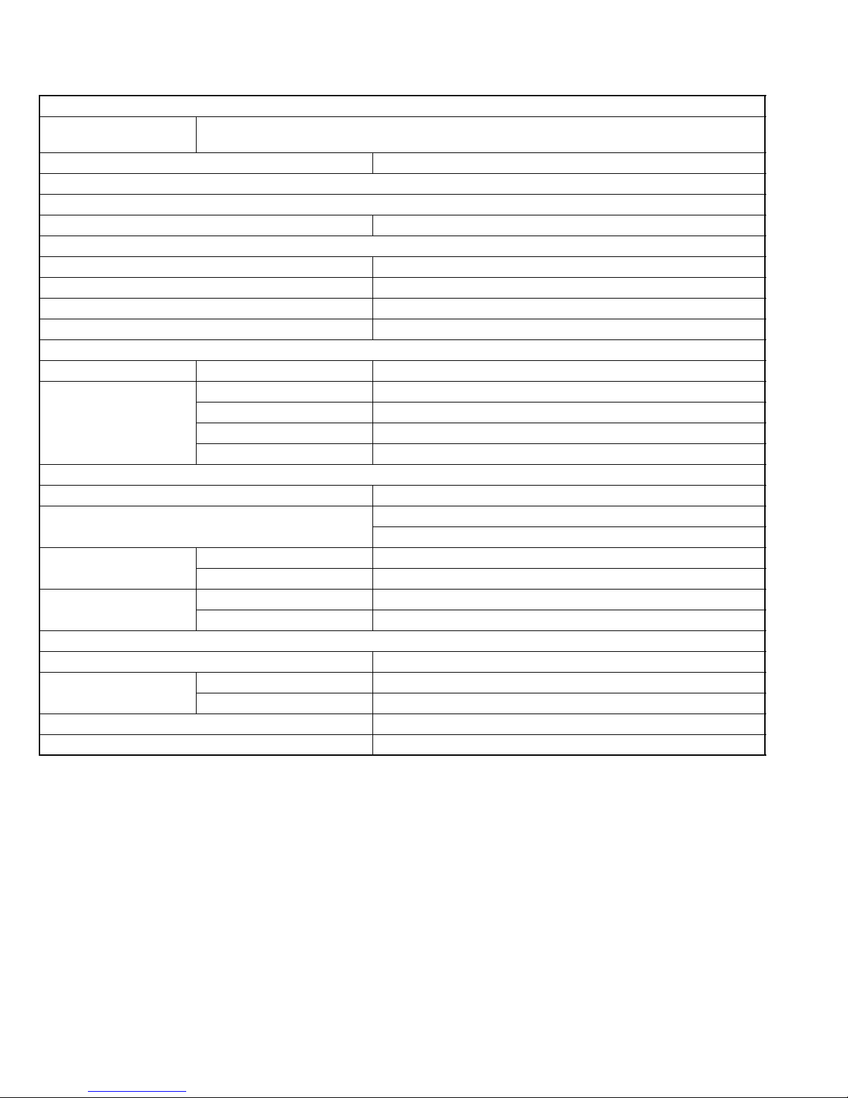
(5) Leakage shock hazard testing
After reassembling the product, always perform an isolation check on the exposed metal parts of the product (antenna terminals, knobs, metal cabinet, screw heads,
headphone jack, control shafts, etc.) to be sure the product
is safe to operate without danger of electrical shock.Do not
use a line isolation transformer during this check.
• Plug the AC line cord directly into the AC outlet. Using a
"Leakage Current Tester", measure the leakage current
from each exposed metal parts of the cabinet, particularly any exposed metal part having a return path to the
chassis, to a known good earth ground. Any leakage current must not exceed 0.5mA AC (r.m.s.).
• Alternate check method
Plug the AC line cord directly into the AC outlet. Use an
AC voltmeter having, 1,000Ω per volt or more sensitivity
in the following manner. Connect a 1,500Ω 10W resistor
paralleled by a 0.15µF AC-type capacitor between an ex-
posed metal part and a known good earth ground.
Measure the AC voltage across the resistor with the AC
voltmeter.
Move the resistor connection to each exposed metal
part, particularly any exposed metal part having a return
path to the chassis, and measure the AC voltage across
the resistor. Now, reverse the plug in the AC outlet and
repeat each measurement. Voltage measured any must
not exceed 0.75 V AC (r.m.s.). This corresponds to 0.5
mA AC (r.m.s.).
AC VOLTMETER
(Having 1000
ohms/volts,
or more sensitivity)
0.15 F AC TYPE
Place this
probe on
1500 10W
Good earth ground
1.2 Warning
(1) This equipment has been designed and manufactured to
meet international safety standards.
(2) It is the legal responsibility of the repairer to ensure that
these safety standards are maintained.
(3) Repairs must be made in accordance with the relevant
safety standards.
(4) It is essential that safety critical components are replaced
by approved parts.
(5) If mains voltage selector is provided, check setting for local
voltage.
1.3 Caution
Burrs formed during molding may be left over on some parts
of the chassis.
Therefore, pay attention to such burrs in the case of preforming repair of this system.
1.4 Critical parts for safety
In regard with component parts appearing on the silk-screen
printed side (parts side) of the PWB diagrams, the parts that are
printed over with black such as the resistor ( ), diode ( )
and ICP ( ) or identified by the " " mark nearby are critical
for safety. When replacing them, be sure to use the parts of the
same type and rating as specified by the manufacturer.
(This regulation dose not Except the J and C version)
each exposed
metal part.
(No.MB725<Rev.001>)1-3
Page 4
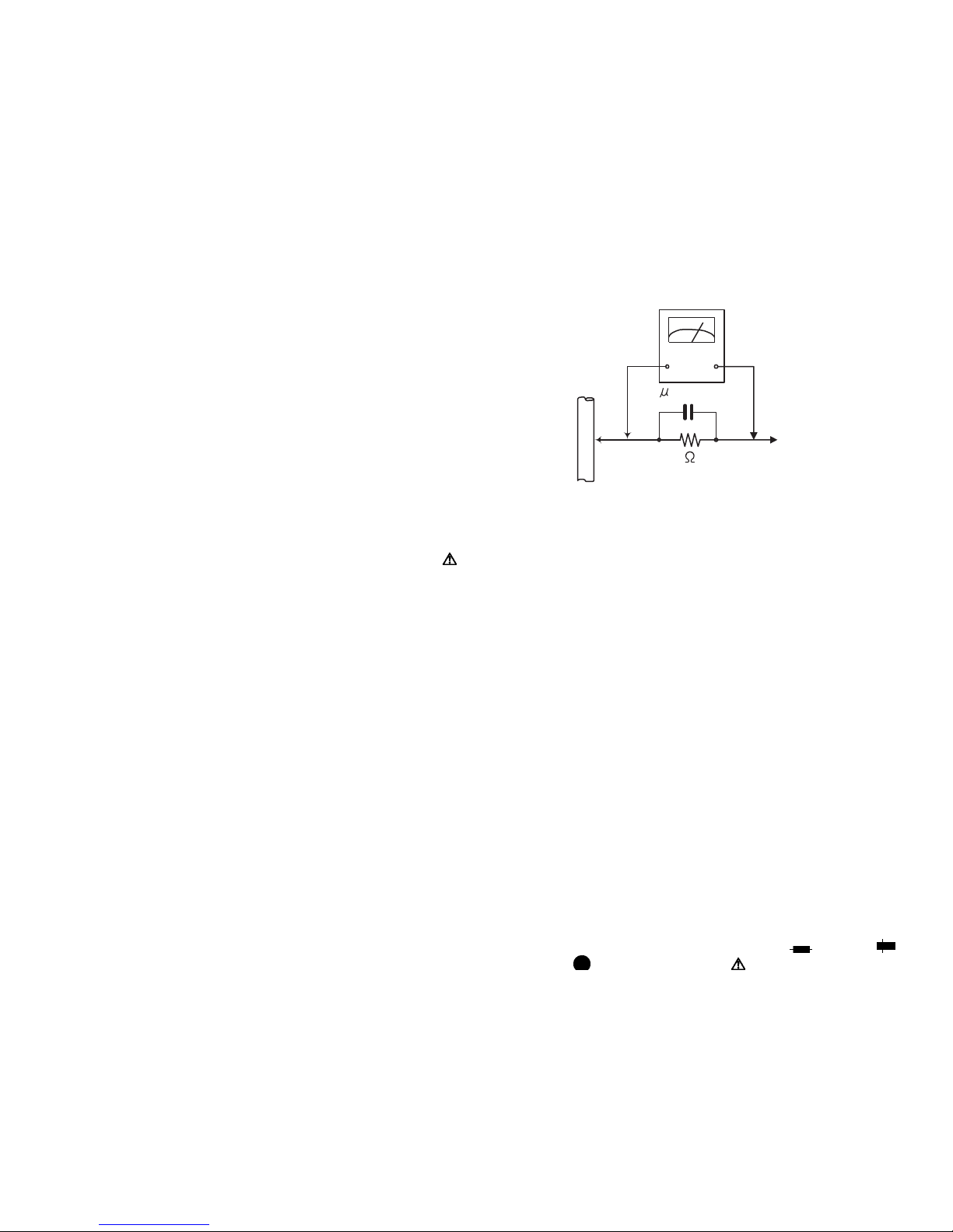
1.5 Preventing static electricity
Electrostatic discharge (ESD), which occurs when static electricity stored in the body, fabric, etc. is discharged, can destroy the laser
diode in the traverse unit (optical pickup). Take care to prevent this when performing repairs.
1.5.1 Grounding to prevent damage by static electricity
Static electricity in the work area can destroy the optical pickup (laser diode) in devices such as laser products.
Be careful to use proper grounding in the area where repairs are being performed.
(1) Ground the workbench
Ground the workbench by laying conductive material (such as a conductive sheet) or an iron plate over it before placing the
traverse unit (optical pickup) on it.
(2) Ground yourself
Use an anti-static wrist strap to release any static electricity built up in your body.
(caption)
Anti-static wrist strap
1M
Conductive material
(conductive sheet) or iron palate
(3) Handling the optical pickup
• In order to maintain quality during transport and before installation, both sides of the laser diode on the replacement optical
pickup are shorted. After replacement, return the shorted parts to their original condition.
(Refer to the text.)
• Do not use a tester to check the condition of the laser diode in the optical pickup. The tester's internal power source can easily
destroy the laser diode.
1.6 Handling the traverse unit (optical pickup)
(1) Do not subject the traverse unit (optical pickup) to strong shocks, as it is a sensitive, complex unit.
(2) Cut off the shorted part of the flexible cable using nippers, etc. after replacing the optical pickup. For specific details, refer to the
replacement procedure in the text. Remove the anti-static pin when replacing the traverse unit. Be careful not to take too long a
time when attaching it to the connector.
(3) Handle the flexible cable carefully as it may break when subjected to strong force.
(4) I t is not possible to adjust the semi-fixed resistor that adjusts the laser power. Do not turn it.
1-4 (No.MB725<Rev.001>)
Page 5
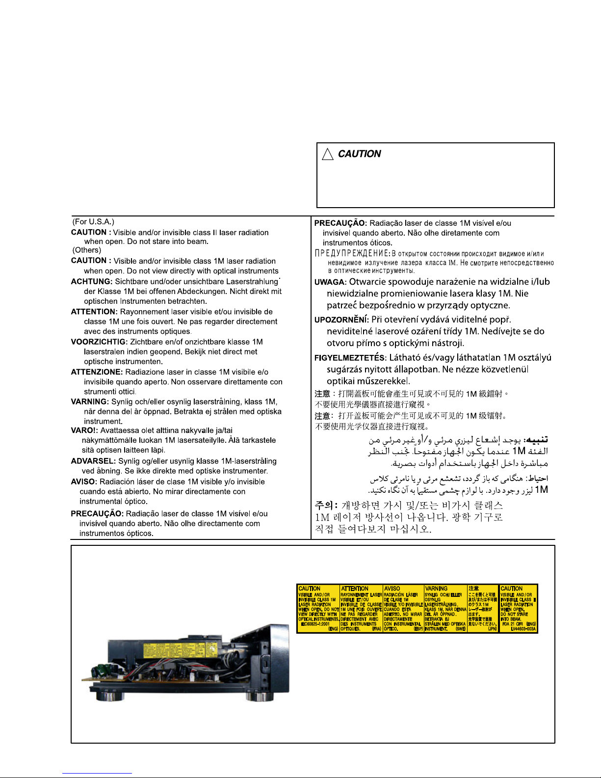
1.7 Important for laser products
1.CLASS 1 LASER PRODUCT
2.CAUTION :
(For U.S.A.) Visible and/or invisible class II laser radiation
when open. Do not stare into beam.
(Others) Visible and/or invisible class 1M laser radiation
when open. Do not view directly with optical instruments.
3.CAUTION : Visible and/or invisible laser radiation when
open and inter lock failed or defeated. Avoid direct
exposure to beam.
4.CAUTION : This laser product uses visible and/or invisible
laser radiation and is equipped with safety switches which
prevent emission of radiation when the drawer is open and
the safety interlocks have failed or are defeated. It is
dangerous to defeat the safety switches.
5.CAUTION : If safety switches malfunction, the laser is able
to function.
6.CAUTION : Use of controls, adjustments or performance of
procedures other than those specified here in may result in
hazardous radiation exposure.
!
Please use enough caution not to
see the beam directly or touch it
in case of an adjustment or operation
check.
REPRODUCTION AND POSITION OF LABELS and PRINT
WARNING LABEL and PRINT
(No.MB725<Rev.001>)1-5
Page 6
SECTION 2
SPECIFIC SERVICE INSTRUCTIONS
This service manual does not describe SPECIFIC SERVICE INSTRUCTIONS.
SECTION 3
DISASSEMBLY
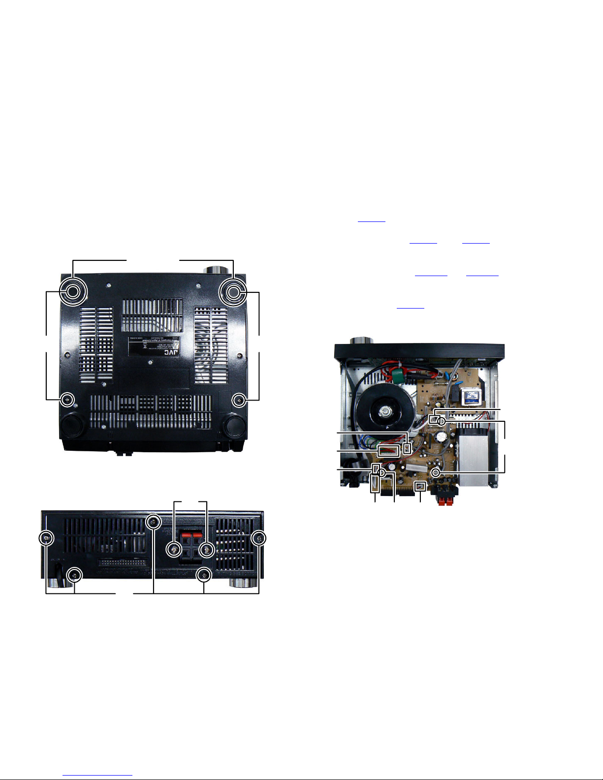
3.1 Amplifier unit (Used model is UX-TB30E)
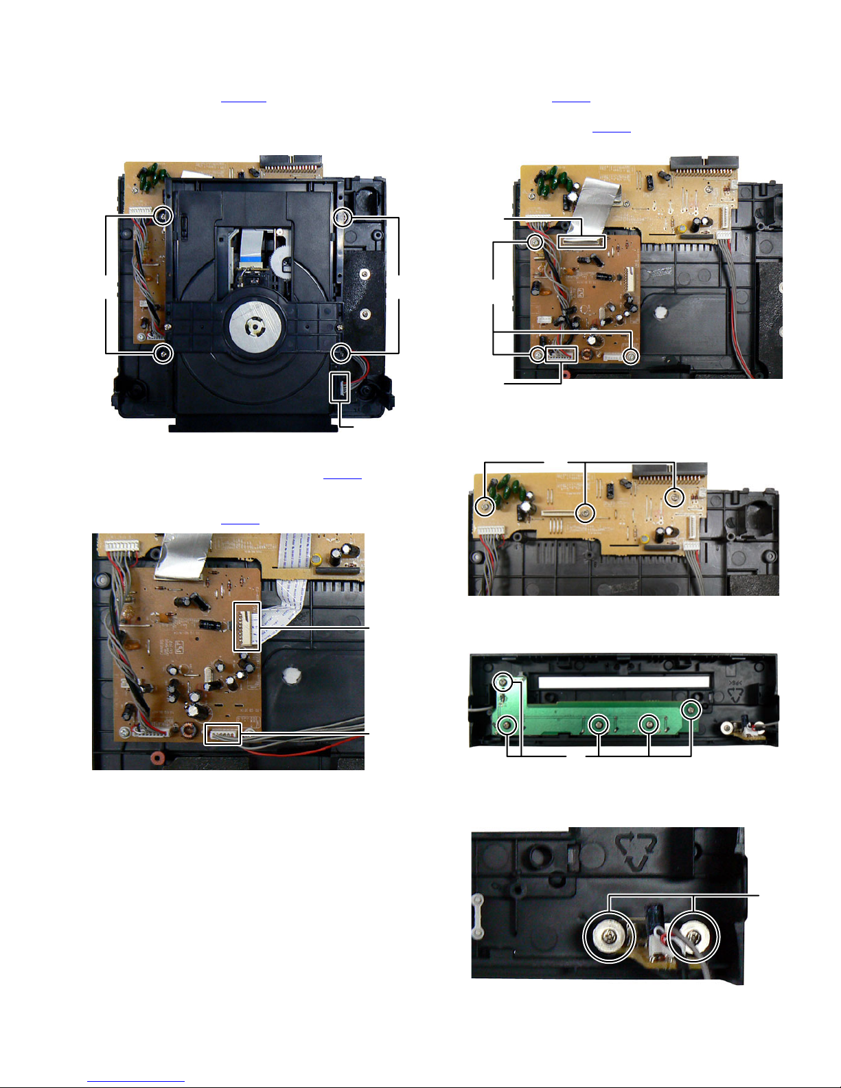
3.1.1 Removing the Top cover (See Fig.1, 2)
(1) Tear off the Rubber foots. (See Fig.1)
(2) Remove the four screws A attaching the Top cover. (See
Fig.1)
Rubber foot
3.1.2 Removing the Main board (See Fig.3, 4)
(1) Disconnect the card wire from Display board connected to
connector CN303
(2) Disconnect the connector wires from Display board con-
nected to connectors CN302 and CN305 of the Main
board. (See Fig.3)
(3) Disconnect the connector wires from Power transformer
connected to connectors CN1101
board. (See Fig.3)
(4) Disconnect the connector wire from Rectifier board con-
nected to connector CN402
(5) Remove the three screws D attaching the Main board. (See
Fig.3)
of the Main board. (See Fig.3)
of the Main board. (See Fig.3)
AA
CN305
CN1101
Fig.1
(3) Remove the five screws B and two screws C attaching the
Rear cover. (See Fig.2)
CN402
and CN1104 of the Main
CN1104
D
C
B
Fig.2
1-6 (No.MB725<Rev.001>)
CN303 CN302
D
Fig.3
Page 7
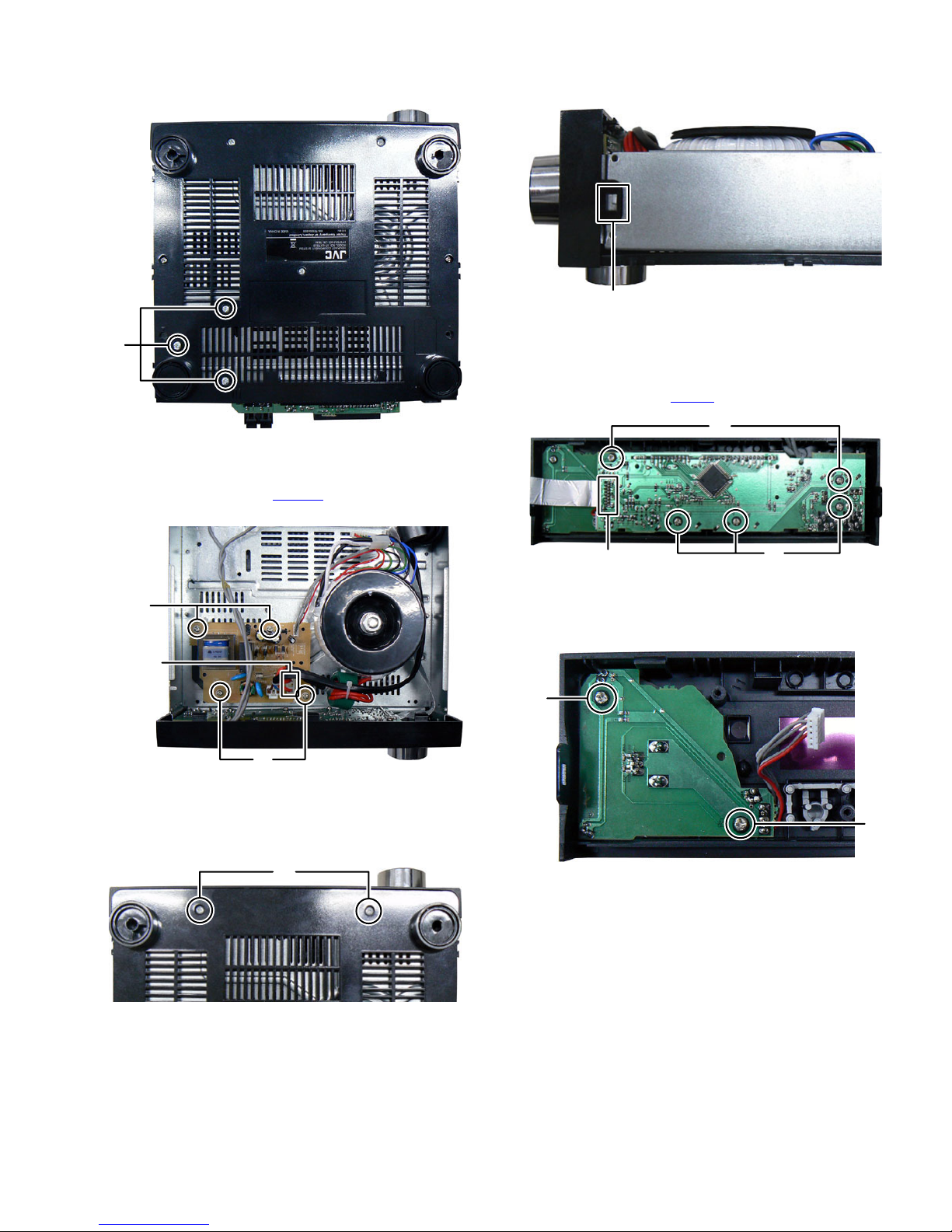
(6) Remove the three screws E attaching the Heat sink. (See
Fig.4)
E
(2) Disengage two hooks a engaged both side of the Front
panel. (See Fig.7)
hook
a
Fig.7
3.1.5 Removing the Display board (See Fig.8)
(1) Remove the five screws H attaching the Display board.
(2) Disconnect the connector wire from Volume board con-
nected to connector CN702
of the Display board.
Fig.4
3.1.3 Removing the Rectifier board (See Fig.5)
(1) Disconnect the connector wire from Power transformer
connected to connector CN1102
(2) Remove the four screws F attaching the Rectifier board.
of the Rectifier board.
F
CN1102
F
Fig.5
3.1.4 Removing the Front panel (See Fig.6, 7)
(1) Remove the two screws G attaching the Front panel. (See
Fig.6)
G
H
CN702
Fig.8
3.1.6 Removing the Rectifier board (See Fig.9)
(1) Remove the Volume knob.
(2) Remove the two screws J attaching the Volume board.
H
J
Fig.9
J
Fig.6
(No.MB725<Rev.001>)1-7
Page 8
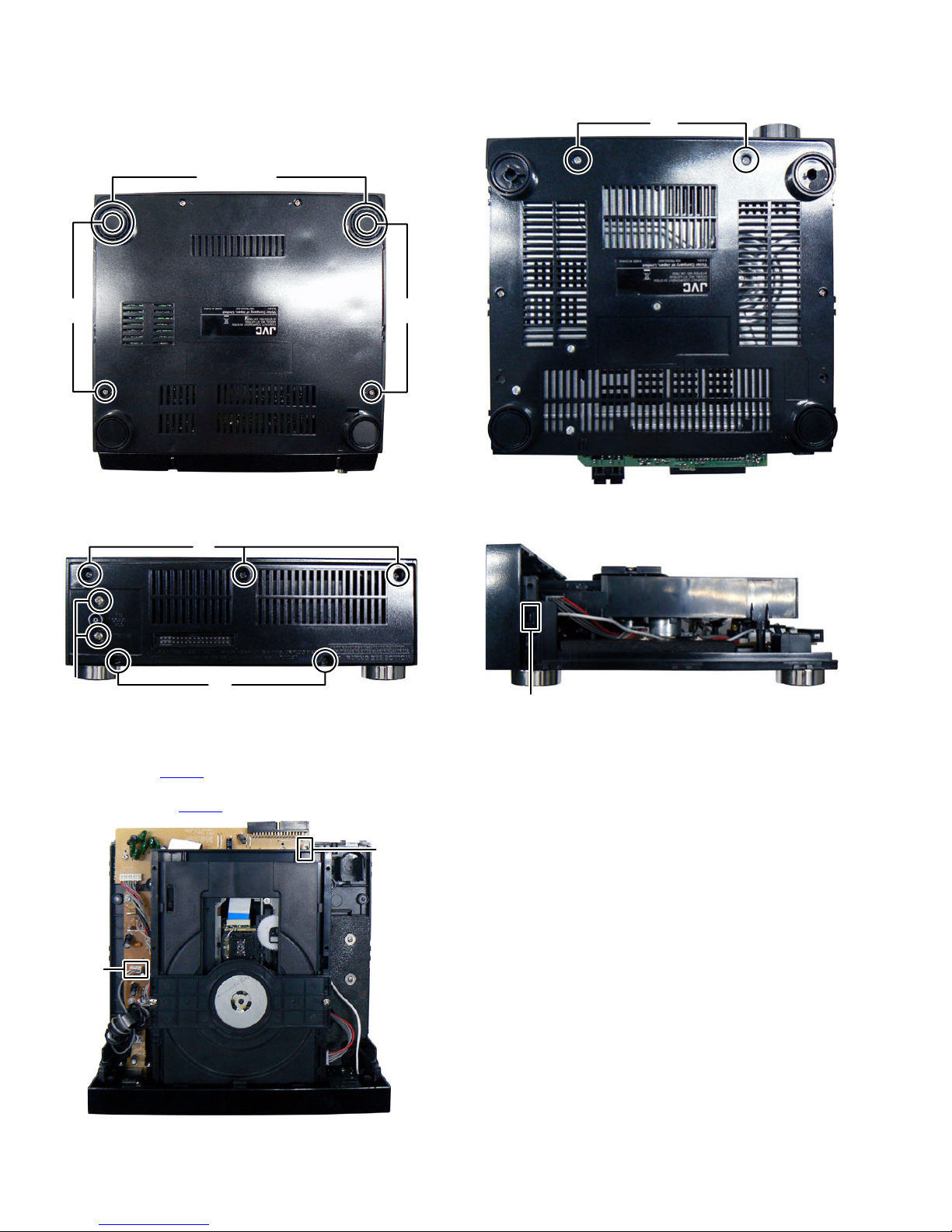
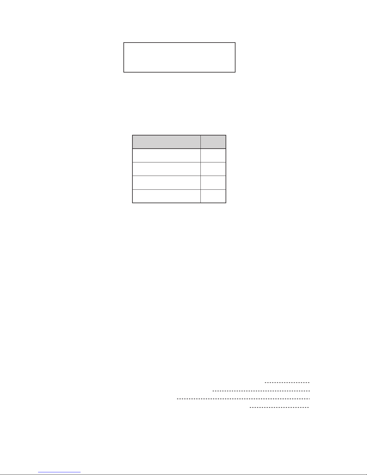
3.2 CD unit (Used model is UX-TB30E)
A
3.2.1 Removing the Top cover (See Fig.1, 2)
(1) Tear off the Rubber foots. (See Fig.1)
(2) Remove the four screws A attaching the Top cover. (See
Fig.1)
Rubber foot
(3) Remove the two screws D attaching the Front panel. (See
Fig.4)
D
A
Fig.1
(3) Remove the five screws B and two screws C attaching the
Rear cover. (See Fig.2)
B
C
3.2.2 Removing the Front panel (See Fig.3, 4, 5)
(1) Disconnect the connector wire from USB board connected
to connector CN603
(2) Disconnect the connector wire from Control board connect-
ed to connector CN703
B
Fig.2
of the CD board. (See Fig.3)
of the Equalizer board. (See Fig.3)
CN703
Fig.4
(4) Disengage two hooks a engaged both side of the Front
panel. (See Fig.5)
hook
a
Fig.5
CN603
Fig.3
1-8 (No.MB725<Rev.001>)
Page 9
3.2.3 Removing the CD mechanism (See Fig.6, 7)
(1) Disconnect the connector wire from Equalizer board con-
nected to connector CN2701
(See Fig.6)
(2) Remove the four screws E attaching the CD mechanism.
(See Fig.6)
of the CD door switch board.
3.2.4 Removing the CD board (See Fig.8)
(1) Disconnect the card wire from Equalizer board connected
to connector CN702
(2) Disconnect the connector wire from Equalizer board con-
nected to connector CN901
(3) Remove the three screws F attaching the CD board.
CN702
of the CD board.
of the CD board.
EE
CN2701
Fig.6
(3) Turnover the CD mechanism, disconnect the card wire
from pickup connected to connector CN905
board. (See Fig.7)
(4) Disconnect the connector wire from CD mechanism con-
nected to connector CN907
of the CD board. (See Fig.7)
of the CD
CN905
F
CN901
Fig.8
3.2.5 Removing the Equalizer board (See Fig.9)
(1) Remove the three screws G attaching the Equalizer board.
G
Fig.9
3.2.6 Removing the Control board (See Fig.10)
(1) Remove the five screws H attaching the Control board.
Fig.7
CN907
H
Fig.10
3.2.7 Removing the USB board (See Fig.11)
(1) Remove the two screws J attaching the USB board.
J
Fig.11
(No.MB725<Rev.001>)1-9
Page 10

SECTION 4
ADJUSTMENT
This service manual does not describe ADJUSTMENT.
SECTION 5
TROUBLESHOOTING
This service manual does not describe TROUBLESHOOTING.
1-10 (No.MB725<Rev.001>)
Page 11

Page 12

Victor Company of Japan, Limited
Home Entertainment Business Division Personal AV Operation 10-1,1chome,Ohwatari-machi,Maebashi-city,371-8543,Japan
(No.MB725<Rev.001>)
Printed in Japan
VSE
Page 13
PARTS LIST
UX-TB30B, UX-TB30E, UX-TB30EN, UX-TB30EV
MODEL MARK
AUX-TB30B
UX-TB30E
UX-TB30EV
* All printed circuit boards and its assemblies are not available as service parts.
B
CUX-TB30EN
D
- Contents -
Exploded view of general assembly and parts list (Block No.M1)
Speaker assembly and parts list (Block No.M2)
Electrical parts list (Block No.01~10)
Packing materials and accessories parts list (Block No.M3)
MB725PAR<Rev.001>
3- 2
3- 6
3- 7
3-13
3-1
Page 14
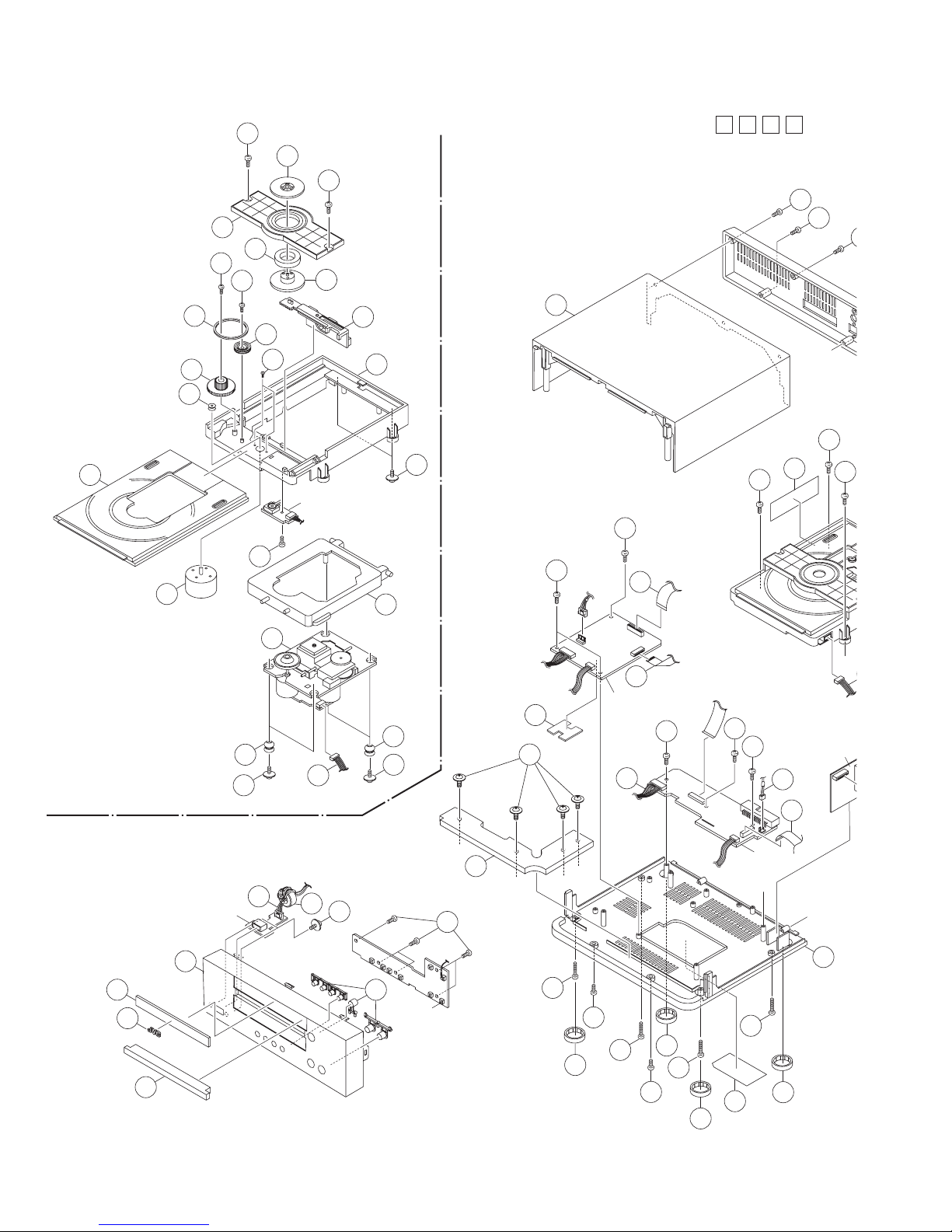
Exploded view of general assembly and parts list
9
d
64
26
64
CD unit section
27
32
58
33
25
22
CD door switch board
14
84
23
28
72
57
78
29
59
Block No.
60
M MM1
97
81
95
95
B
97
97
77
CD BOX section
4
6
15
USB board
1
30
85
62
45
31
80
44
b
61
60
b
46
c
24
a
e
f
48
CD board
c
A
98
d
90
90
EQ board
g
50
Tuner board
51
z
30
85
86
f
90
49
e
40
A
91
g
9
Control board
55
34
96
55
96
55
34
55
82
B
13
34
34
3-2
Page 15

95
95
89
95
AMP unit section
68
39
14
12
37
65
37
65
37
37
7
97
A
board
11
a
97
73
93
93
79
n
93
Rectifer board
73
71
93
h
w
63
92
63
92
63
92
j
52
54
B
67
w
69
r
s
63
m
u
Main board
66
70
h
k
53
17
p
n
75
76
p
56
d
35
38
36
r
94
19
z
m
20
j
7
42
94
s
u
43
k
21
94
8
10
2
3
3
6
5
99
18
t
Volume board
Display board
16
47
t
87
87
87
41
74
34
88
34
74
88
34
34
74
83
The parts without symbol number are not service.
3-3
Page 16

General Assembly
Symbol No. Part No. Part Name Description Local
1 5TB-300000-002 CONTROL FRONT CABINET
2 5TB-300000-001 DISPLAY FRONT CABINET
3 5TB-300000-000 DISPLAY LENS
4 5TB-300200-001 CONTROL LENS
5 5TB-307000-001 VOLUME KNOB
6 500-081000-000 JVC MARK (x2)
7 5TB-332000-000 VFD BRACKET
8 5TB-308000-000 POWER KNOB
9 5TB-302000-000 CONTROL KNOB
10 5TB-351000-000 FUNCTION KNOB
11 5TB-386000-001 UP BACK COVER
12 5TB-386000-002 DOWN BACK COVER
13 5TB-302000-001 PEDESTAL CABINET
14 5TB-300820-000 TOP CABINET (x2)
15 5TB-349000-000 CD DOOR
16 5TB-302000-002 PEDESTAL CABINET
17 530-026200-000 LINE CORE HOLD
18 244-E05260-060 HSG 5PINS 60mm
19 244-A04300-300 WIRE 4PINS 30cm
20 244-A03780-300 WIRE 3PINS 30cm
21 235-165250-110 FFC CABLE 16PINS
22 500-047000-000 CD MECHA BRACKET
23 500-049100-000 CD PLATE
24 500-026300-000 CD MECHA COVER
25 500-036000-000 SLIDE PIECE
26 500-200000-000 CD CHUCK PLATE
27 500-048300-000 CHUCK PLATE BRACKET
28 500-000100-200 BIG GEAR
29 500-000100-100 LITTER GEAR
30 458-328840-220 RUBBER SILICON (BLACK) HARDNESS(x4)
31 356-110003-091 CD DECK
32 473-300160-500 CD MAGNET RING
33 500-100000-000 CD CHUCK HOLDER
34 5TB-303000-090 RING (x8)
35 419-030240-030 SHIELD PLATE(FRONT)
36 419-306430-030 SHIELD PLATE(BACK)
37 238-130100-602 SCREW 3x10mm PB(x5)
38 408-222193-020 METAL CABINET
39 408-TB3040-040 HEAT SINK
40 408-TB3000-010 PLUMMET METAL
41 5TB-300560-050 LENS BACK LIGHT
42 220-025100-015 VFD DISPLAY
43 152-302369-070 TRANSFORMER TB3023FS
44 244-B06260-150 HSG 6PINS 150mm
45 244-A04780-350 WIRE 4PINS 35cm
46 235-235070-110 FFC CABLE 23PINS
47 5TB-3010120-000 LIGHT BULT COVER
48 235-160130-110 FFC CABLE 16PINS 13cm
49 244-092600-130 HSG 9PINS 130mm
50 244-E02280-240 WIRE 2PINS 24cm
51 235-109250-112 FFC CABLE 10PINS 1.25mm
52 244-A04260-150 WIRE 4PINS 15cm
53 222-290190-155 FERRITE BEAD
54 151-240000-302 POWER CORD A
54 151-230000-200 POWER CORD B,C,D
55 238-130150-602 SCREW 3x15mm PB(x4)
56 244-E05260-170 WIRE 5PINS 17cm
57 238-117050-631 SCREW 1.7x5mm PWA
58 238-117050-632 SCREW 1.7x5mm PWB
59 238-117040-203 SCREW 1.7x4mm BM(x2)
60 238-130060-602 SCREW 3x6mm PB(x3)
61 238-126080-631 SCREW 2.6x8mm PWA(x2)
62 238-126080-602 SCREW 2.6x8mm PB
63 238-130080-202A SCREW 3x8mm BB(x6)
64 238-130100-602 SCREW 3x10mm PB(x2)
65 238-130100-202A SCREW 3x10mm BB(x2)
66 408-360230-120 HEAT SINK
67 408-043030-250 HEAT SINK
68 361-401012-002 HEAT FAN
69 231-902630-253 FUSE FS1102 6.3A 250V
70 231-902160-253 FUSE FS1103 1.6A 250V
71 231-902200-251 FUSE FS1101 2A 250V
72 519-024300-000 MOTOR PULLEY NSX-1900
73 238-130120-602 SCREW ST 3x12mm PB(x4)
Block No. [M][1][M][M]
3-4
Page 17

Symbol No. Part No. Part Name Description Local
74 238-130150-602 SCREW 3x15mm PB(x4)
75 880-TB8002-040 VOLTAGE HOLE PLATE FOR MAIN PCB
76 466-103069-050 VOLTAGE HOLE PLATE FOR POWER PC
77 360-055133-002 MOTOR RF-300CA-10510
78 466-235013-013 STRAP FOR MOTOR
79 152-402328-000 POWER TRANSF PT1101 230V
80 222-250150-120 FERRITE BEAD
81 LV44603-003A CAUTION LABEL
82 898-TB3000-020 NAME PLATE
83 898-TB3000-010 NAME PLATE
84 238-126080-631 SCREW 2.6x8mm PWA(x2)
85 238-126080-631 SCREW 2.6x8mm PWA(x4)
86 238-126080-631 SCREW 2.6x8mm PWA(x4)
87 238-130080-202A SCREW 3x8mm BB(x3)
88 238-130080-202A SCREW 3x8mm BB(x5)
89 238-130080-202A SCREW 3x8mm BB(x2)
90 238-126080-602 SCREW 2.6x8mm PB(x3)
91 238-126080-602 SCREW 2.6x8mm PB(x5)
92 238-126080-602 SCREW 2.6x8mm PB(x3)
93 238-126080-602 SCREW 2.6x8mm PB(x4)
94 238-126080-602 SCREW 2.6x8mm PB(x5)
95 238-130100-602 SCREW 3x10mm PB(x5)
96 238-130100-602 SCREW 3x10mm PB(x2)
97 238-130100-602 SCREW 3x10mm PB(x4)
98 408-270230-008 HEAT SINK
99 238-126080-602 SCREW 2.6x8mm PB(x2)
3-5
Page 18

Speaker assembly and parts list
4
Block No.
M
M
M
2
10
9
6
8
5
4
7
4
3
1
2
The parts without symbol number are not service.
Speaker
Symbol No. Part No. Part Name Description Local
Block No. [M][2][M][M]
1 500-081000-000 JVC MARK (x2)
2 5TB-340000-000 SPEAKER NET BRACKET L/R (x2)
3 5TB-341000-000 SPEAKER FRONT L/R (x2)
4 238-140100-631 SCREW 4x10 mm PWA(x12)
5 458-TB3100-010 RUBBER HOLDER (x12)
6 5TB-301000-000 DECORATION PIECE (x2)
7 5TB-301000-001 SPEAKER BRACKET (x2)
8 154-496200-600 SPEAKER (x2)
9 669-TB3000-000 SPEAKER BOX (x2)
10 520-938000-000 SPEAKER PIPE (x2)
3-6
Page 19

Electrical parts list
Main board
Block No. [0][1]
Symbol No.
IC302 210-008947-000 IC
IC303 210-001308-000 IC
IC401 210-007805-022 IC CD7805CS
IC402 210-007809-039 ZENER IC
IC403 210-007812-039 ZENER IC
IC404 210-007809-039 ZENER IC
Q301 307-008050-030 TRANSISTOR 8050C/D
Q304 307-009014-030 TRANSISTOR 9014C
Q305 307-008050-030 TRANSISTOR 8050C/D
Q306 307-009014-030 TRANSISTOR 9014C
Q307 307-009014-030 TRANSISTOR 9014C
Q308 307-009014-030 TRANSISTOR 9014C
Q309 307-008550-020 TRANSISTOR
Q313 207-191936-913 TRANSISTOR
Q314 207-191936-913 TRANSISTOR
Q403 207-181185-560 TRANSISTOR
Q406 307-008050-030 TRANSISTOR 8050C/D
Q409 307-009014-030 TRANSISTOR 9014C
Q410 207-008550-020 TRANSISTOR
D301 206-104148-000 DIODE IN-4148
D302 206-305817-000 RECTIFIER IN5817
D303 206-104148-000 DIODE IN-4148
D304 206-104148-000 DIODE IN-4148
D305 206-104148-000 DIODE IN-4148
D306 206-304001-000 RECTIFIER IN-4001
D307 206-304001-000 RECTIFIER IN-4001
D308 206-305817-000 RECTIFIER IN5817
D309 206-104148-000 DIODE IN-4148
D1106 206-304001-000 RECTIFIER IN-4001
D1107 206-304001-000 RECTIFIER IN-4001
DB1101 206-308040-000
DB1102 206-308040-000
C304 302-341045-550 C CAPACITOR 0.1uF/50V
C308 004-062262-216 E CAPACITOR 22uF/16V
C313 004-074772-225 E CAPACITOR 470uF/25V
C319 004-054752-216 E CAPACITOR 4.7uF/16V
C320 004-054752-216 E CAPACITOR 4.7uF/16V
C321 004-054752-216 E CAPACITOR 4.7uF/16V
C322 004-054752-216 E CAPACITOR 4.7uF/16V
C323 004-072272-216 E CAPACITOR 220uF/16V
C324 302-312715-550 C CAPACITOR 270pF/50V
C325 302-312715-550 C CAPACITOR 270pF/50V
C326 004-072272-216 E CAPACITOR 220uF/16V
C328 302-332235-550 C CAPACITOR 0.022uF/50V
C329 004-072272-210 E CAPACITOR 220uF/10V
C330 004-072272-210 E CAPACITOR 220uF/10V
C331 302-332235-550 C CAPACITOR 0.022uF/50V
C340 004-064762-216 E CAPACITOR 47uF/16V
C401 004-072272-216 E CAPACITOR 220uF/16V
C402 302-341045-550 C CAPACITOR 0.1uF/50V
C403 004-072272-250 E CAPACITOR 220uF/50V
C406 302-341045-550 C CAPACITOR 0.1uF/50V
C407 004-072272-210 E CAPACITOR 220uF/10V
C409 004-074772-216 E CAPACITOR 470uF/16V
C411 004-064762-216 E CAPACITOR 47uF/16V
C412 004-072272-225 E CAPACITOR 220uF/25V
C413 004-072272-225 E CAPACITOR 220uF/25V
C414 302-341045-550 C CAPACITOR 0.1uF/50V
C415 004-071072-225 E CAPACITOR 100uF/25V
C436 302-312715-550 C CAPACITOR 270pF/50V
C438 302-341045-550 C CAPACITOR 0.1uF/50V
C439 302-312715-550 C CAPACITOR 270pF/50V
C440 302-341045-550 C CAPACITOR 0.1uF/50V
C441 302-341045-550 C CAPACITOR 0.1uF/50V
C442 302-312715-550 C CAPACITOR 270pF/50V
C443 302-341045-550 C CAPACITOR 0.1uF/50V
C444 302-312715-550 C CAPACITOR 270pF/50V
C451 302-331035-550 C CAPACITOR 0.01uF/50V
C452 302-331035-550 C CAPACITOR 0.01uF/50V
Part No. Part Name Description Local
SILICON BRIDGE RECTIFIERS
SILICON BRIDGE RECTIFIERS
8.0A
8.0A
Symbol No.
C453 302-311015-550 C CAPACITOR 100pF/50V
C454 302-311015-550 C CAPACITOR 100pF/50V
C455 302-341045-550 C CAPACITOR 0.1uF/50V
C456 302-341045-550 C CAPACITOR 0.1uF/50V
C457 302-341045-550 C CAPACITOR 0.1uF/50V
C458 302-312715-550 C CAPACITOR 270pF/50V
C459 302-312715-550 C CAPACITOR 270pF/50V
C464 302-341045-550 C CAPACITOR 0.1uF/50V
C465 302-301005-550 C CAPACITOR 10pF/50V
C467 302-312715-550 C CAPACITOR 270pF/50V
C474 302-312215-550 C CAPACITOR 220pF/50V
C475 302-312215-550 C CAPACITOR 220pF/50V
C477 302-341045-550 C CAPACITOR 0.1uF/50V
C478 302-312715-550 C CAPACITOR 270pF/50V
C479 302-312715-550 C CAPACITOR 270pF/50V
C487 004-071072-216 E CAPACITOR 100uF/16V
C488 004-071072-216 E CAPACITOR 100uF/16V
C490 004-064762-216 E CAPACITOR 47uF/16V
C492 004-061062-225 E CAPACITOR 10uF/25V
C493 302-341045-550 C CAPACITOR 0.1uF/50V
C500 302-311015-550 C CAPACITOR 100pF/50V
C501 302-311015-550 C CAPACITOR 100pF/50V
C506 302-311015-550 C CAPACITOR 100pF/50V
C612 004-061062-216 E CAPACITOR 10uF/16V
C727 004-061062-216 E CAPACITOR 10uF/16V
C1108 302-341045-550 C CAPACITOR 0.1uF/50V
C1109 302-341045-550 C CAPACITOR 0.1uF/50V
C1112 004-083382-225 E CAPACITOR 3300uF/25V
C1113 004-086882-235 E CAPACITOR 6800uF/35V
R301 301-322225-016 RESISTOR 2.2k
R302 301-322225-016 RESISTOR 2.2k
R303 301-324725-016 RESISTOR 4.7k
R304 301-324725-016 RESISTOR 4.7k
R305 301-322725-016 RESISTOR 2.7K
R306 301-324325-016 RESISTOR 4.3k
R307 301-324725-016 RESISTOR 4.7k
R308 301-324725-016 RESISTOR 4.7k
R309 301-324725-016 RESISTOR 4.7k
R310 301-300005-016 RESISTOR 0
R311 301-324725-016 RESISTOR 4.7k
R314 301-324725-016 RESISTOR 4.7k
R318 301-300005-016 RESISTOR 0
R319 301-351055-016 RESISTOR 1M
R320 301-328225-016 RESISTOR 8.2k
R321 301-322725-016 RESISTOR 2.7K
R324 301-324325-016 RESISTOR 4.3k
R325 301-332235-016 RESISTOR 22k
R327 301-351055-016 RESISTOR 1M
R328 301-341245-016 RESISTOR 120k
R332 301-332735-016 RESISTOR 27k
R336 301-331035-016 RESISTOR 10k
R340 301-341245-016 RESISTOR 120k
R342 301-334735-016 RESISTOR 47k
R343 301-334735-016 RESISTOR 47k
R347 301-324725-016 RESISTOR 4.7k
R348 301-331035-016 RESISTOR 10k
R351 301-351055-016 RESISTOR 1M
R391 301-324725-016 RESISTOR 4.7k
R392 301-321025-016 RESISTOR 1k
R393 301-331035-016 RESISTOR 10k
R401 201-000220-185 RESISTOR 2.2
R402 301-331035-016 RESISTOR 10k
R403 301-321025-016 RESISTOR 1k
R404 201-000220-105 RESISTOR 2.2
R405 201-000220-105 RESISTOR 2.2
R406 301-331035-016 RESISTOR 10k
R408 301-324725-016 RESISTOR 4.7k
R409 301-322025-016 RESISTOR 2K
R413 301-332235-016 RESISTOR 22k
R416 201-002200-125 RESISTOR 22
R417 201-011500-145 RESISTOR 150
R419 301-321025-016 RESISTOR 1k
R421 301-334735-016 RESISTOR 47k
R422 301-324725-016 RESISTOR 4.7k
R423 201-001000-105 RESISTOR 10
Part No. Part Name Description Local
Ω
1/16W
Ω
1/16W
Ω
Ω
Ω
Ω
Ω
Ω
Ω
Ω
Ω
Ω
Ω
Ω
Ω
Ω
Ω
Ω
Ω
Ω
Ω
Ω
Ω
Ω
Ω
Ω
Ω
1/16W
Ω
1/16W
Ω
1/16W
Ω
1/16W
Ω
1/16W
Ω
1/16W
Ω
1/16W
Ω
1/16W
Ω
1/16W
Ω
1/16W
Ω
1/16W
1/16W
Ω
1/16W
Ω
1/16W
Ω
1/16W
1/16W
1/16W
Ω
1/16W
1/16W
1/16W
Ω
1/16W
1/16W
1/16W
Ω
1/16W
1/16W
1/16W
Ω
1/16W
1/16W
1/16W
1/8W
1/16W
1/16W
1W
1W
1/16W
Ω
1/16W
1/16W
1/16W
1/2W
1/4W
1/16W
1/16W
Ω
1/16W
1W
3-7
Page 20

Symbol No.
Part No. Part Name Description Local
Symbol No.
Part No. Part Name Description Local
R445 301-321025-016 RESISTOR 1kΩ 1/16W
R446 301-321025-016 RESISTOR 1k
R449 301-322725-016 RESISTOR 2.7K
R450 301-322725-016 RESISTOR 2.7K
R451 301-332235-016 RESISTOR 22k
R452 301-324725-016 RESISTOR 4.7k
R456 301-324725-016 RESISTOR 4.7k
R459 301-322025-016 RESISTOR 2K
R460 201-000220-145 RESISTOR 2.2
R465 301-325625-016 RESISTOR 5.6K
R466 301-324725-016 RESISTOR 4.7k
R1104 201-000220-145 RESISTOR 2.2
R1105 201-000220-145 RESISTOR 2.2
L301 226-000470-002 CHOKE COIL
L302 226-000470-002 CHOKE COIL
L303 226-000470-002 CHOKE COIL
L304 226-000470-002 CHOKE COIL
CN302 233-030200-020 CONNECTOR 3PINS2.0mm
CN305 233-040200-020 CONNECTOR 4PINS 2.0mm
CN402 233-040200-020 CONNECTOR 4PINS 2.0mm
CN404 233-020200-025 CONNECTOR 2PINS 2.5mm
CN708 232-160190-310 FFC CONNECTOR 16P
CN1101 233-080200-025 CONNECTOR 8PINS 2.5mm
CN1104 233-020080-040 CONNECTOR 2PINS 4.0mm
JK301 232-340508-325 FFC CONNECTOR 34P
JK306 242-200408-288 SPEAKER TERMINAL
ZD402 206-200270-102 Z DIODE 27V 1/2W
ZD403 206-200047-102 Z DIODE 4.7V 1/2W
ZD405 206-200068-102 Z DIODE 6.8V 1/2W
ZD406 206-200056-102 Z DIODE 5.6V 1/2W
Ω
1/16W
Ω
Ω
Ω
1/16W
Ω
Ω
Ω
1/16W
Ω
1/4W
Ω
Ω
Ω
1/4W
Ω
1/4W
1/16W
1/16W
1/16W
1/16W
1/16W
1/16W
CD board
Block No. [0][2]
Symbol No.
IC401 310-001526-100 IC AIC1526
IC404 310-001117-104 IC
IC701 310-002402-102 IC
IC901 310-005675-128 IC
IC902 310-002520-008 IC
IC903 310-009258-128 IC SA9258PH (3V3)
U701 310-006812-132 IC
Q901 307-008050-030 TRANSISTOR 8050C/D
Q902 307-008050-030 TRANSISTOR 8050C/D
Q903 207-008550-020 TRANSISTOR
Q904 307-008550-020 TRANSISTOR
Q905 307-008050-030 TRANSISTOR 8050C/D
Q906 307-008050-030 TRANSISTOR 8050C/D
D410 206-304001-000 RECTIFIER IN-4001
D701 206-305819-000 RECTIFIER IN-5819
D702 206-104148-000 DIODE IN-4148
D902 206-104148-000 DIODE IN-4148
D903 206-104148-000 DIODE IN-4148
D904 206-104148-000 DIODE IN-4148
D905 206-104148-000 DIODE IN-4148
C407 302-311015-550 C CAPACITOR 100pF/50V
C411 302-341045-550 C CAPACITOR 0.1uF/50V
C441 004-061062-216 E CAPACITOR 10uF/16V
C442 302-341045-550 C CAPACITOR 0.1uF/50V
C701 302-341045-550 C CAPACITOR 0.1uF/50V
C702 302-341045-550 C CAPACITOR 0.1uF/50V
C703 302-341045-550 C CAPACITOR 0.1uF/50V
C705 302-302005-550 C CAPACITOR 20pF/50V
C706 302-302005-550 C CAPACITOR 20pF/50V
C707 302-301805-550 C CAPACITOR 18pF/50V
C708 302-301805-550 C CAPACITOR 18pF/50V
C709 302-311015-550 C CAPACITOR 100pF/50V
C710 302-311015-550 C CAPACITOR 100pF/50V
Part No. Part Name Description Local
AZ1117 TO-252-2(1)
C711 302-311015-550 C CAPACITOR 100pF/50V
C712 302-311015-550 C CAPACITOR 100pF/50V
C713 302-311015-550 C CAPACITOR 100pF/50V
C714 302-331035-550 C CAPACITOR 0.01uF/50V
C715 302-331035-550 C CAPACITOR 0.01uF/50V
C716 302-321025-550 C CAPACITOR 0.001uF/50V
C717 302-331035-550 C CAPACITOR 0.01uF/50V
C718 302-302005-550 C CAPACITOR 20pF/50V
C901 302-311015-550 C CAPACITOR 100pF/50V
C902 302-306805-550 C CAPACITOR 68pF/50V
C903 302-306805-550 C CAPACITOR 68pF/50V
C904 302-306805-550 C CAPACITOR 68pF/50V
C905 302-306805-550 C CAPACITOR 68pF/50V
C906 302-321025-550 C CAPACITOR 0.001uF/50V
C907 302-311015-550 C CAPACITOR 100pF/50V
C908 302-311015-550 C CAPACITOR 100pF/50V
C909 302-311015-550 C CAPACITOR 100pF/50V
C910 302-331035-550 C CAPACITOR 0.01uF/50V
C911 302-341045-550 C CAPACITOR 0.1uF/50V
C912 302-341045-550 C CAPACITOR 0.1uF/50V
C913 302-341045-550 C CAPACITOR 0.1uF/50V
C914 302-341045-550 C CAPACITOR 0.1uF/50V
C915 302-341045-550 C CAPACITOR 0.1uF/50V
C916 302-341045-550 C CAPACITOR 0.1uF/50V
C917 302-351055-550 C CAPACITOR 1uF/50V
C918 302-341045-550 C CAPACITOR 0.1uF/50V
C919 302-341045-550 C CAPACITOR 0.1uF/50V
C920 302-341045-550 C CAPACITOR 0.1uF/50V
C921 302-338231-150 C CAPACITOR 0.082uF/50V
C922 302-338231-150 C CAPACITOR 0.082uF/50V
C924 302-341045-550 C CAPACITOR 0.1uF/50V
C925 302-303005-550 C CAPACITOR 30pF/50V
C927 302-341045-550 C CAPACITOR 0.1uF/50V
C928 302-341045-550 C CAPACITOR 0.1uF/50V
C929 302-303005-550 C CAPACITOR 30pF/50V
C930 302-341045-550 C CAPACITOR 0.1uF/50V
C931 302-341045-550 C CAPACITOR 0.1uF/50V
C933 302-341045-550 C CAPACITOR 0.1uF/50V
C934 302-341045-550 C CAPACITOR 0.1uF/50V
C935 302-331035-550 C CAPACITOR 0.01uF/50V
C936 302-341045-550 C CAPACITOR 0.1uF/50V
C937 302-341045-550 C CAPACITOR 0.1uF/50V
C938 302-331035-550 C CAPACITOR 0.01uF/50V
C939 302-344742-250 C CAPACITOR 0.47uF/50V
C940 302-316815-550 C CAPACITOR 680pF/50V
C941 302-316815-550 C CAPACITOR 680pF/50V
C942 302-334735-550 C CAPACITOR 0.047uF/50V
C943 302-341045-550 C CAPACITOR 0.1uF/50V
C954 302-341045-550 C CAPACITOR 0.1uF/50V
C956 302-341045-550 C CAPACITOR 0.1uF/50V
C957 302-341045-550 C CAPACITOR 0.1uF/50V
C958 302-341045-550 C CAPACITOR 0.1uF/50V
C959 302-341045-550 C CAPACITOR 0.1uF/50V
C960 302-341045-550 C CAPACITOR 0.1uF/50V
C961 004-074772-210 E CAPACITOR 470uF/10V
C962 004-061062-216 E CAPACITOR 10uF/16V
C963 302-341045-550 C CAPACITOR 0.1uF/50V
C964 302-351055-550 C CAPACITOR 1uF/50V
C965 302-351055-550 C CAPACITOR 1uF/50V
C966 004-061062-216 E CAPACITOR 10uF/16V
C967 004-071072-210 E CAPACITOR 100uF/10V
C968 302-351055-550 C CAPACITOR 1uF/50V
C969 004-061062-216 E CAPACITOR 10uF/16V
C970 004-064762-210 E CAPACITOR 47uF/10V
C971 004-061062-216 E CAPACITOR 10uF/16V
C972 004-072272-216 E CAPACITOR 220uF/16V
C973 302-351055-550 C CAPACITOR 1uF/50V
C974 004-054752-250 E CAPACITOR 4.7uF/50V
C975 004-054752-250 E CAPACITOR 4.7uF/50V
C977 004-064762-210 E CAPACITOR 47uF/10V
C978 004-081082-210 E CAPACITOR 1000uF/10V
C979 302-351055-550 C CAPACITOR 1uF/50V
C980 004-051052-250 E CAPACITOR 1uF/50V
C983 302-311015-550 C CAPACITOR 100pF/50V
C984 302-311015-550 C CAPACITOR 100pF/50V
C985 302-331035-550 C CAPACITOR 0.01uF/50V
C986 302-301005-550 C CAPACITOR 10pF/50V
C987 302-306805-550 C CAPACITOR 68pF/50V
3-8
Page 21

Symbol No.
Part No. Part Name Description Local
Symbol No.
Part No. Part Name Description Local
C988 302-306805-550 C CAPACITOR 68pF/50V
C989 302-306805-550 C CAPACITOR 68pF/50V
C990 302-341045-550 C CAPACITOR 0.1uF/50V
C991 302-311515-550 C CAPACITOR 150pF/50V
C992 004-054752-250 E CAPACITOR 4.7uF/50V
C994 302-321025-550 C CAPACITOR 0.001uF/50V
C995 302-311015-550 C CAPACITOR 100pF/50V
C996 003-041048-250 C CAPACITOR 0.1uF/50V
C997 302-341045-550 C CAPACITOR 0.1uF/50V
C998 302-331035-550 C CAPACITOR 0.01uF/50V
C999 004-061062-216 E CAPACITOR 10uF/16V
TC701 004-072272-216 E CAPACITOR 220uF/16V
Ω
R416 301-331035-016 RESISTOR 10k
R438 301-300005-016 RESISTOR 0
R439 301-300005-016 RESISTOR 0
R470 001-000225-012 TAPPING RESISTOR 2.2
R701 301-341045-016 RESISTOR 100k
R705 301-321025-016 RESISTOR 1k
R706 301-331035-016 RESISTOR 10k
R707 322-134000-221 FERRITE BEAD
R708 301-331035-016 RESISTOR 10k
R709 301-321025-016 RESISTOR 1k
R710 301-331035-016 RESISTOR 10k
R711 301-321025-016 RESISTOR 1k
R712 301-321025-016 RESISTOR 1k
R713 301-321025-016 RESISTOR 1k
R714 301-321025-016 RESISTOR 1k
R715 301-321025-016 RESISTOR 1k
R716 301-321025-016 RESISTOR 1k
R717 301-321025-016 RESISTOR 1k
R718 301-321025-016 RESISTOR 1k
R719 301-321025-016 RESISTOR 1k
R720 301-321025-016 RESISTOR 1k
R721 301-321025-016 RESISTOR 1k
R722 301-321025-016 RESISTOR 1k
R723 301-300005-016 RESISTOR 0
R724 301-351055-016 RESISTOR 1M
R739 301-321025-016 RESISTOR 1k
R740 301-324725-016 RESISTOR 4.7k
R741 301-324725-016 RESISTOR 4.7k
R742 301-321025-016 RESISTOR 1k
R743 301-321025-016 RESISTOR 1k
R744 322-134000-220 FERRITE BEAD
R745 322-134000-220 FERRITE BEAD
R746 301-331035-016 RESISTOR 10k
R748 322-134000-221 FERRITE BEAD
R750 301-321025-016 RESISTOR 1k
R751 301-321025-016 RESISTOR 1k
R752 322-134000-221 FERRITE BEAD
R753 301-300005-016 RESISTOR 0
R912 301-331035-016 RESISTOR 10k
R913 301-331035-016 RESISTOR 10k
R914 301-331035-016 RESISTOR 10k
R915 301-331035-016 RESISTOR 10k
R916 301-331035-016 RESISTOR 10k
R917 301-331035-016 RESISTOR 10k
R918 301-331035-016 RESISTOR 10k
R919 301-331035-016 RESISTOR 10k
R921 322-134000-221 FERRITE BEAD
R922 301-331035-016 RESISTOR 10k
R923 301-321025-016 RESISTOR 1k
R924 301-331035-016 RESISTOR 10k
R925 322-134000-221 FERRITE BEAD
R926 301-331035-016 RESISTOR 10k
R927 322-134000-221 FERRITE BEAD
R928 301-341045-016 RESISTOR 100k
R929 301-341045-016 RESISTOR 100k
R930 301-300005-016 RESISTOR 0
R931 301-300005-016 RESISTOR 0
R932 301-300005-016 RESISTOR 0
R934 301-313315-016 RESISTOR 330
R935 301-301005-016 RESISTOR 10
R936 301-341045-016 RESISTOR 100k
R937 301-333335-016 RESISTOR 33k
R938 301-331035-016 RESISTOR 10kΩ 1/16W
R939 301-331035-016 RESISTOR 10k
R941 301-324725-016 RESISTOR 4.7k
Ω
1/16W
Ω
1/16W
Ω
Ω
Ω
Ω
Ω
Ω
Ω
Ω
Ω
Ω
Ω
Ω
Ω
Ω
Ω
Ω
Ω
Ω
Ω
1/16W
Ω
Ω
Ω
Ω
Ω
Ω
Ω
Ω
1/16W
Ω
Ω
Ω
Ω
Ω
Ω
Ω
Ω
Ω
Ω
Ω
Ω
Ω
1/16W
Ω
1/16W
Ω
1/16W
Ω
Ω
Ω
Ω
1/16W
1/2W
Ω
1/16W
1/16W
1/16W
1/16W
1/16W
1/16W
1/16W
1/16W
1/16W
1/16W
1/16W
1/16W
1/16W
1/16W
1/16W
1/16W
1/16W
1/16W
1/16W
1/16W
Ω
1/16W
Ω
1/16W
1/16W
1/16W
1/16W
1/16W
1/16W
1/16W
1/16W
1/16W
1/16W
1/16W
1/16W
1/16W
1/16W
1/16W
1/16W
1/16W
1/16W
Ω
1/16W
Ω
1/16W
1/16W
1/16W
Ω
1/16W
1/16W
Ω
1/16W
R942 301-300005-016 RESISTOR 0Ω 1/16W
R944 301-100005-014 RESISTOR 0
R945 301-325125-016 RESISTOR 5.1k
R946 301-333335-016 RESISTOR 33k
R947 301-341045-016 RESISTOR 100kΩ 1/16W
R948 301-324725-016 RESISTOR 4.7k
R949 301-324725-016 RESISTOR 4.7k
R957 301-321025-016 RESISTOR 1k
R958 301-321025-016 RESISTOR 1k
R966 301-321025-016 RESISTOR 1k
R968 301-334735-016 RESISTOR 47k
R969 301-300005-016 RESISTOR 0
R970 301-321025-016 RESISTOR 1k
R971 301-321025-016 RESISTOR 1k
R981 301-300005-016 RESISTOR 0
R982 301-300005-016 RESISTOR 0
R984 301-324725-016 RESISTOR 4.7k
R985 301-314715-016 RESISTOR 470
R986 301-332235-016 RESISTOR 22k
R987 301-331035-016 RESISTOR 10k
R988 301-321025-016 RESISTOR 1k
R989 301-331035-016 RESISTOR 10k
R990 301-331035-016 RESISTOR 10k
R991 301-331035-016 RESISTOR 10k
R993 301-300005-016 RESISTOR 0
R994 301-324725-016 RESISTOR 4.7k
R995 301-321025-016 RESISTOR 1k
R996 301-331035-016 RESISTOR 10k
R997 301-331035-016 RESISTOR 10k
R998 301-321025-016 RESISTOR 1k
R999 301-321025-016 RESISTOR 1k
L900 322-134000-221 FERRITE BEAD
L901 226-002600-000 CHOKE COIL
L902 322-134000-221 FERRITE BEAD
L905 322-134000-221 FERRITE BEAD
L906 322-134000-221 FERRITE BEAD
L907 322-134000-221 FERRITE BEAD
L908 322-134000-221 FERRITE BEAD
L909 322-134000-221 FERRITE BEAD
L910 322-134000-221 FERRITE BEAD
L911 322-134000-221 FERRITE BEAD
L912 322-134000-221 FERRITE BEAD
L913 322-134000-221 FERRITE BEAD
L914 322-134000-221 FERRITE BEAD
L915 322-134000-221 FERRITE BEAD
L916 322-134000-221 FERRITE BEAD
L917 322-134000-221 FERRITE BEAD
L918 322-134000-221 FERRITE BEAD
L919 322-134000-221 FERRITE BEAD
L931 322-134000-220 FERRITE BEAD
L932 322-134000-220 FERRITE BEAD
L933 301-300005-016 RESISTOR 0
L944 326-230000-202 COIL
L945 326-230000-202 COIL
CN603 233-040200-020 CONNECTOR 4PINS 2.0mm
CN702 232-230200-310 FFC CONNECTOR FFC23P 1.0mm
CN901 233-090200-020 HEADER 9PINS 2.0mm
CN905 232-160190-210 FFC CONNECTOR FFC16PINS 1.0mm
CN907 233-060200-020 CONNECTOR 6PINS 2.0mm
X701 228-368000-002 RESONATOR 3.68MHz
X702 229-327680-292 CRYSTAL 32.768KHz
X901 229-169344-002 CRYSTAL 16.9344 MHz
Ω
1/4W
Ω
Ω
Ω
Ω
Ω
Ω
1/16W
Ω
Ω
Ω
1/16W
Ω
1/16W
Ω
Ω
Ω
Ω
Ω
Ω
Ω
Ω
1/16W
Ω
Ω
Ω
Ω
Ω
Ω
1/16W
Ω
1/16W
Ω
1/16W
Ω
1/16W
1/16W
1/16W
1/16W
1/16W
1/16W
1/16W
Ω
1/16W
1/16W
1/16W
1/16W
1/16W
1/16W
1/16W
1/16W
Ω
1/16W
1/16W
1/16W
1/16W
1/16W
1/16W
Display board
Block No. [0][3]
Symbol No.
IC701 310-016311-154 IC
Q701 307-009014-030 TRANSISTOR 9014C
Q702 307-008550-020 TRANSISTOR
Part No. Part Name Description Local
3-9
Page 22

Symbol No.
Part No. Part Name Description Local
Symbol No.
Part No. Part Name Description Local
Q703 307-008050-030 TRANSISTOR 8050C/D
Q704 307-008550-020 TRANSISTOR
Q710 307-008550-020 TRANSISTOR
D706 206-304001-000 RECTIFIER IN-4001
D707 206-304001-000 RECTIFIER IN-4001
C375 302-331035-550 C CAPACITOR 0.01uF/50V
C376 302-321025-550 C CAPACITOR 0.001uF/50V
C377 302-331035-550 C CAPACITOR 0.01uF/50V
C445 302-321025-550 C CAPACITOR 0.001uF/50V
C446 302-321025-550 C CAPACITOR 0.001uF/50V
C460 302-341045-550 C CAPACITOR 0.1uF/50V
C468 302-341045-550 C CAPACITOR 0.1uF/50V
C469 302-341045-550 C CAPACITOR 0.1uF/50V
C470 302-312215-550 C CAPACITOR 220pF/50V
C471 302-312215-550 C CAPACITOR 220pF/50V
C702 302-341045-550 C CAPACITOR 0.1uF/50V
C704 302-341045-550 C CAPACITOR 0.1uF/50V
C705 004-164762-216 E CAPACITOR 47uF/16V
C706 302-341045-550 C CAPACITOR 0.1uF/50V
C707 004-064762-225 E CAPACITOR 47uF/25V
C709 302-311015-550 C CAPACITOR 100pF/50V
C730 302-311015-550 C CAPACITOR 100pF/50V
C731 302-311015-550 C CAPACITOR 100pF/50V
C733 302-311015-550 C CAPACITOR 100pF/50V
C753 302-341045-550 C CAPACITOR 0.1uF/50V
C754 004-164762-216 E CAPACITOR 47uF/16V
C755 302-341045-550 C CAPACITOR 0.1uF/50V
C756 302-311015-550 C CAPACITOR 100pF/50V
C757 302-341045-550 C CAPACITOR 0.1uF/50V
C758 302-341045-550 C CAPACITOR 0.1uF/50V
C759 302-341045-550 C CAPACITOR 0.1uF/50V
C764 302-311015-550 C CAPACITOR 100pF/50V
C765 302-311015-550 C CAPACITOR 100pF/50V
C767 302-311015-550 C CAPACITOR 100pF/50V
C768 302-311015-550 C CAPACITOR 100pF/50V
C769 302-311015-550 C CAPACITOR 100pF/50V
C770 302-341045-550 C CAPACITOR 0.1uF/50V
C771 302-161061-116 C CAPACITOR 10uF/16V
C772 302-161061-116 C CAPACITOR 10uF/16V
Ω
Ω
Ω
Ω
Ω
Ω
Ω
Ω
Ω
1/16W
Ω
1/16W
Ω
1/16W
Ω
1/16W
Ω
1/16W
Ω
1/16W
Ω
1/16W
Ω
1/16W
1/16W
1/2W
1/2W
Ω
1/16W
Ω
1/16W
Ω
1/16W
Ω
1/16W
Ω
1/16W
Ω
1/16W
1/16W
1/16W
1/16W
Ω
1/16W
Ω
Ω
1/16W
Ω
1/16W
1/16W
Ω
1/16W
Ω
1/16W
Ω
1/16W
Ω
1/16W
Ω
1/16W
Ω
1/16W
Ω
1/16W
Ω
1/16W
R380 301-322725-016 RESISTOR 2.7K
R382 301-332235-016 RESISTOR 22k
R383 301-311215-016 RESISTOR 120
R384 301-311215-016 RESISTOR 120
R386 301-342745-016 RESISTOR 270k
R387 301-342745-016 RESISTOR 270k
R388 301-322225-016 RESISTOR 2.2k
R389 301-322225-016 RESISTOR 2.2k
R390 301-321025-016 RESISTOR 1k
R701 201-000560-125 RESISTOR 5.6
R702 201-001000-125 RESISTOR 10
R704 301-335635-016 RESISTOR 56k
R708 301-331035-016 RESISTOR 10k
R711 301-325625-016 RESISTOR 5.6K
R712 301-332735-016 RESISTOR 27k
R716 301-311015-016 RESISTOR 100
R717 301-331035-016 RESISTOR 10k
R718 301-300000-000 RESISTOR 0
R719 301-332235-016 RESISTOR 22kΩ 1/16W
R720 301-321025-016 RESISTOR 1k
R721 301-321025-016 RESISTOR 1k
R722 301-321025-016 RESISTOR 1k
R761 301-311015-016 RESISTOR 100
R764 301-338235-016 RESISTOR 82k
R769 301-321025-016 RESISTOR 1kΩ 1/16W
R773 301-322225-016 RESISTOR 2.2k
R774 301-328225-016 RESISTOR 8.2k
R776 301-321025-016 RESISTOR 1k
R777 301-344745-016 RESISTOR 470k
R778 301-331035-016 RESISTOR 10k
R779 301-331035-016 RESISTOR 10k
R784 301-331035-016 RESISTOR 10k
R785 301-331035-016 RESISTOR 10k
R786 301-331035-016 RESISTOR 10k
R787 301-331035-016 RESISTOR 10k
R788 301-331035-016 RESISTOR 10k
L305 221-045030-014 FERRITE BEAD
L306 221-045030-014 FERRITE BEAD
L307 221-045030-014 FERRITE BEAD
L308 221-045030-014 FERRITE BEAD
L309 221-045030-014 FERRITE BEAD
L310 221-045030-014 FERRITE BEAD
L311 221-045030-014 FERRITE BEAD
L701 301-321025-016 RESISTOR 1k
L702 301-321025-016 RESISTOR 1k
L703 301-321025-016 RESISTOR 1k
L704 322-134000-221 FERRITE BEAD
CN303 232-160190-210 FFC CONNECTOR 16P
CN702 233-051200-020 CONNECTOR 5PINS 2.0mm
IR701 206-100338-112 DIODE 3.3V
JK302 240-135610-902 EARPHONE JACK JY-3561
JK304 240-135610-902 EARPHONE JACK JY-3561
LED701 227-080300-800 LED RED
LED702 227-080300-800 LED RED
SW701 217-060650-500 TACT SWITCH
SW702 217-060650-500 TACT SWITCH
SW707 217-060650-500 TACT SWITCH
SW711 217-060650-500 TACT SWITCH
SW714 217-060650-500 TACT SWITCH
SW715 217-060650-500 TACT SWITCH
VFD701 220-025100-015 VFD DISPLAY 25100-1A11 15MM
Ω
1/16W
Ω
1/16W
Ω
1/16W
EQ board
Block No. [0][4]
Symbol No.
IC301 310-007314-100 IC
IC502 210-001641-000 IC
Q401 307-008550-020 TRANSISTOR
D401 206-104148-000 DIODE IN-4148
D402 206-104148-000 DIODE IN-4148
C301 302-314715-550 C CAPACITOR 470pF/50V
C302 302-314715-550 C CAPACITOR 470pF/50V
C351 004-062262-216 E CAPACITOR 22uF/16V
C352 004-081082-210 E CAPACITOR 1000uF/10V
C353 302-322725-550 C CAPACITOR 0.027uF/50V
C354 004-054752-216 E CAPACITOR 4.7uF/16V
C355 004-054752-216 E CAPACITOR 4.7uF/16V
C356 005-041041-199 M CAPACITOR 0.1uF/100V
C357 004-054752-216 E CAPACITOR 4.7uF/16V
C358 302-322725-550 C CAPACITOR 0.027uF/50V
C359 005-041041-199 M CAPACITOR 0.1uF/100V
C361 005-041041-199 M CAPACITOR 0.1uF/100V
C362 005-041041-199 M CAPACITOR 0.1uF/100V
C363 302-351055-550 C CAPACITOR 1uF/50V
C364 302-351055-550 C CAPACITOR 1uF/50V
C365 302-312715-550 C CAPACITOR 270pF/50V
C366 302-312715-550 C CAPACITOR 270pF/50V
C367 005-041041-199 M CAPACITOR 0.1uF/100V
C368 005-041041-199 M CAPACITOR 0.1uF/100V
C370 302-351055-550 C CAPACITOR 1uF/50V
C371 302-351055-550 C CAPACITOR 1uF/50V
C372 302-351055-550 C CAPACITOR 1uF/50V
C373 004-054752-216 E CAPACITOR 4.7uF/16V
C374 302-351055-550 C CAPACITOR 1uF/50V
C378 302-341045-550 C CAPACITOR 0.1uF/50V
C382 326-230000-202 COIL
C383 326-230000-202 COIL
C384 326-230000-202 COIL
C385 326-230000-202 COIL
C386 302-321025-550 C CAPACITOR 0.001uF/50V
C387 302-331035-550 C CAPACITOR 0.01uF/50V
C388 302-341045-550 C CAPACITOR 0.1uF/50V
C389 302-341045-550 C CAPACITOR 0.1uF/50V
Part No. Part Name Description Local
3-10
Page 23

Symbol No.
C390 302-321025-550 C CAPACITOR 0.001uF/50V
C391 302-321025-550 C CAPACITOR 0.001uF/50V
C392 302-321025-550 C CAPACITOR 0.001uF/50V
C393 302-321025-550 C CAPACITOR 0.001uF/50V
C394 301-300005-016 RESISTOR 0
C395 302-326821-150 C CAPACITOR 0.0068uF/50V
C396 302-326821-150 C CAPACITOR 0.0068uF/50V
C397 302-341045-550 C CAPACITOR 0.1uF/50V
C398 302-321025-550 C CAPACITOR 0.001uF/50V
C399 302-321025-550 C CAPACITOR 0.001uF/50V
C400 302-341045-550 C CAPACITOR 0.1uF/50V
C427 302-341045-550 C CAPACITOR 0.1uF/50V
C428 004-072272-216 E CAPACITOR 220uF/16V
C430 302-341045-550 C CAPACITOR 0.1uF/50V
C431 302-341045-550 C CAPACITOR 0.1uF/50V
C432 302-341045-550 C CAPACITOR 0.1uF/50V
C433 302-341045-550 C CAPACITOR 0.1uF/50V
C434 302-341045-550 C CAPACITOR 0.1uF/50V
C435 302-341045-550 C CAPACITOR 0.1uF/50V
C461 302-311515-550 C CAPACITOR 150pF/50V
C463 302-321025-550 C CAPACITOR 0.001uF/50V
C480 302-311015-550 C CAPACITOR 100pF/50V
C481 302-311015-550 C CAPACITOR 100pF/50V
C489 302-341045-550 C CAPACITOR 0.1uF/50V
C491 302-341045-550 C CAPACITOR 0.1uF/50V
C498 302-341045-550 C CAPACITOR 0.1uF/50V
C505 302-311015-550 C CAPACITOR 100pF/50V
C507 302-311015-550 C CAPACITOR 100pF/50V
C600 301-300005-016 RESISTOR 0
C610 301-300005-016 RESISTOR 0
C611 004-072272-216 E CAPACITOR 220uF/16V
R361 301-311015-016 RESISTOR 100
R362 301-326825-016 RESISTOR 6.8k
R363 301-322225-016 RESISTOR 2.2kΩ 1/16W
R364 301-322225-016 RESISTOR 2.2k
R365 301-326825-016 RESISTOR 6.8k
R366 301-324725-016 RESISTOR 4.7kΩ 1/16W
R367 301-324725-016 RESISTOR 4.7k
R368 301-326825-016 RESISTOR 6.8k
R369 301-326825-016 RESISTOR 6.8k
R375 301-300005-016 RESISTOR 0Ω 1/16W
R376 301-300005-016 RESISTOR 0
R378 301-311015-016 RESISTOR 100
R379 301-311015-016 RESISTOR 100
R418 301-321025-016 RESISTOR 1k
R429 301-324725-016 RESISTOR 4.7k
R432 301-300005-016 RESISTOR 0
R433 301-300005-016 RESISTOR 0
R439 301-321025-016 RESISTOR 1k
R440 301-321025-016 RESISTOR 1k
R441 301-300005-016 RESISTOR 0
R442 301-321025-016 RESISTOR 1k
R443 301-321025-016 RESISTOR 1k
R447 301-201005-018 RESISTOR 10
R448 301-201005-018 RESISTOR 10
R457 301-300005-016 RESISTOR 0
R467 001-001005-014 TAPPING RESISTOR 10
R468 301-321025-016 RESISTOR 1k
R469 301-300005-016 RESISTOR 0
R474 301-300005-016 RESISTOR 0
R735 301-321025-016 RESISTOR 1k
R736 301-321025-016 RESISTOR 1k
R737 301-321025-016 RESISTOR 1k
R747 301-300005-016 RESISTOR 0
R772 301-322225-016 RESISTOR 2.2k
L503 326-230000-202 COIL
L504 326-230000-202 COIL
L510 226-001000-002 CHOKE COIL 10uH
CN504 232-100160-312 FFC CONNECTOR FFC10PINS 1.25mm
CN703 233-020200-020 CONNECTOR 2PINS 2.0mm
CN709 232-230200-310 FFC CONNECTOR FFC23P 1.0mm
JK305 232-340508-325 FFC CONNECTOR FFC34PINS 2.8mm
ZD401 206-200062-102 Z DIODE 6.2V 1/2W
ZD501 206-200051-102 Z DIODE 5.1V 1/2W
Part No. Part Name Description Local
Ω
1/16W
Ω
1/16W
Ω
1/16W
Ω
1/16W
Ω
Ω
1/16W
Ω
Ω
1/16W
Ω
Ω
Ω
1/16W
Ω
1/16W
Ω
1/16W
Ω
1/16W
Ω
1/16W
Ω
1/16W
Ω
1/16W
Ω
1/16W
Ω
1/16W
Ω
1/16W
Ω
1/16W
Ω
1/16W
Ω
1/8W
Ω
1/8W
Ω
1/16W
Ω
1/4
Ω
1/16W
Ω
1/16W
Ω
1/16W
Ω
1/16W
Ω
1/16W
Ω
1/16W
Ω
1/16W
Ω
1/16W
Rectifer board
Block No. [0][5]
Symbol No.
IC1101 310-001117-104 IC AZ1117 TO-252-2(1)
Q1102 307-009014-030 TRANSISTOR 9014C
Q1103 307-009015-013 TRANSISTOR
D1101 206-104148-000 DIODE IN-4148
D1102 206-304001-000 RECTIFIER IN-4001
D1103 206-304001-000 RECTIFIER IN-4001
D1104 206-304001-000 RECTIFIER IN-4001
D1105 206-304001-000 RECTIFIER IN-4001
D1108 206-305817-000 RECTIFIER IN5817
C1101 003-034738-250 C CAPACITOR 0.047uF/50V
C1102 003-034738-250 C CAPACITOR 0.047uF/50V
C1103 003-034738-250 C CAPACITOR 0.047uF/50V
C1104 003-034738-250 C CAPACITOR 0.047uF/50V
C1105 004-081082-225 E CAPACITOR 1000uF/25V
C1106 003-031038-240 C CAPACITOR 0.01uF/400V
C1107 003-031038-240 C CAPACITOR 0.01uF/400V
C1111 004-081082-225 E CAPACITOR 1000uF/25V
C1114 004-071072-216 E CAPACITOR 100uF/16V
C1115 004-062262-216 E CAPACITOR 22uF/16V
C1116 302-341045-550 C CAPACITOR 0.1uF/50V
C1117 302-341045-550 C CAPACITOR 0.1uF/50V
C1118 302-341045-550 C CAPACITOR 0.1uF/50V
R1101 301-311815-016 RESISTOR 180
R1102 301-324725-016 RESISTOR 4.7kΩ 1/16W
R1103 301-311815-016 RESISTOR 180
R1106 301-311815-016 RESISTOR 180
R1107 301-311815-016 RESISTOR 180
R1108 301-311815-016 RESISTOR 180
R1109 301-322025-016 RESISTOR 2KΩ 1/16W
R1110 301-322025-016 RESISTOR 2K
R1111 301-311815-016 RESISTOR 180
R1112 301-311815-016 RESISTOR 180
R1113 301-311815-016 RESISTOR 180
L1101 226-054000-000 CHOKE COIL 540uH
CN1102 233-020119-080 CONNECTOR 2PINS 7.92mm
CN1103 410-020180-100 CONTACT PIN A2361W 2 PINS S35
RL1101 280-700600-120 RELAY
Part No. Part Name Description Local
Ω
Ω
Ω
Ω
Ω
Ω
1/16W
Ω
Ω
Ω
Tuner board
Block No. [0][6]
Symbol No.
IC101 310-004705-120 IC
D103 306-000099-003 TRANSISTOR
C101 302-402205-550 C CAPACITOR 22pF/50V
C102 302-441041-150 C CAPACITOR 0.1uF/50V
C103 302-441041-150 C CAPACITOR 0.1uF/50V
C104 302-402205-550 C CAPACITOR 22pF/50V
C105 302-402205-550 C CAPACITOR 22pF/50V
C106 302-341045-550 C CAPACITOR 0.1uF/50V
C109 302-303305-550 C CAPACITOR 33pF/50V
C110 302-303305-550 C CAPACITOR 33pF/50V
C112 302-331035-550 C CAPACITOR 0.01uF/50V
C114 302-351055-550 C CAPACITOR 1uF/50V
C115 302-351055-550 C CAPACITOR 1uF/50V
C116 302-331831-150 C CAPACITOR 0.018uF/50V
C117 302-331831-150 C CAPACITOR 0.018uF/50V
C120 004-071072-210 E CAPACITOR 100uF/10V
R101 301-300005-016 RESISTOR 0
R102 301-301005-016 RESISTOR 10
Part No. Part Name Description Local
Ω
1/16W
Ω
1/16W
3-11
Page 24

Symbol No.
Part No. Part Name Description Local
Symbol No.
Part No. Part Name Description Local
R103 301-434735-016 RESISTOR 47k
R104 301-431035-016 RESISTOR 10k
R105 301-431035-016 RESISTOR 10k
R107 301-300005-016 RESISTOR 0Ω 1/16W
R108 301-300005-016 RESISTOR 0
R109 301-311015-016 RESISTOR 100
R117 322-134000-221 FERRITE BEAD
R119 322-134000-221 FERRITE BEAD
R120 301-300005-016 RESISTOR 0
R131 301-321025-016 RESISTOR 1k
CF101 208-880108-750 BAND PASS FILTER 75
CN101 232-100160-312 FFC CONNECTOR FFC10PINS 1.25mm
JK101 242-010000-050 FM FM ANTENNA JACK
X101 229-327680-200 CRYSTAL 32.768KHz
Ω
Ω
Ω
Ω
1/16W
Ω
Ω
1/16W
Ω
1/16W
Ω
1/16W
Control board
Block No. [0][7]
Symbol No.
C751 302-331035-550 C CAPACITOR 0.01uF/50V
R762 301-328225-016 RESISTOR 8.2k
R765 301-321025-016 RESISTOR 1k
R767 301-338235-016 RESISTOR 82k
R768 301-322225-016 RESISTOR 2.2kΩ 1/16W
R770 301-325625-016 RESISTOR 5.6K
R771 301-331235-016 RESISTOR 12k
R775 301-311015-016 RESISTOR 100
Part No. Part Name Description Local
Ω
1/16W
Ω
1/16W
Ω
Ω
1/16W
Ω
1/16W
Ω
1/16W
C483 302-321025-550 C CAPACITOR 0.001uF/50V
C601 004-061062-216 E CAPACITOR 10uF/16V
C602 302-321025-550 C CAPACITOR 0.001uF/50V
L601 322-134000-220 FERRITE BEAD
L603 322-134000-220 FERRITE BEAD
L604 301-300000-000 RESISTOR 0
L605 301-300000-000 RESISTOR 0
JK601 253-040145-120 USB CONNECTOR 4PIN 2.0mm
Ω
Ω
CD door switch board
Block No. [1][0]
Symbol No.
C613 302-321025-550 C CAPACITOR 0.001uF/50V
C614 302-321025-550 C CAPACITOR 0.001uF/50V
C615 302-321025-550 C CAPACITOR 0.001uF/50V
CN2701 233-051200-020 CONNECTOR 5PINS 2.0mm
SW2701 218-110215-109 PUSH SWITCH LF-109
Part No. Part Name Description Local
SW712 217-060650-500 TACT SWITCH
SW713 217-060650-500 TACT SWITCH
SW716 217-060650-500 TACT SWITCH
SW717 217-060650-500 TACT SWITCH
SW718 217-060650-500 TACT SWITCH
SW719 217-060650-500 TACT SWITCH
SW720 217-060650-500 TACT SWITCH
Volume board
Block No. [0][8]
Symbol No.
C416 302-341045-550 C CAPACITOR 0.1uF/50V
C417 302-341045-550 C CAPACITOR 0.1uF/50V
C418 302-341045-550 C CAPACITOR 0.1uF/50V
C419 302-311015-550 C CAPACITOR 100pF/50V
C420 302-311015-550 C CAPACITOR 100pF/50V
R470 301-312715-016 RESISTOR 270
R471 301-312715-016 RESISTOR 270
R472 301-312715-016 RESISTOR 270
VR401 270-122105-152 ROTARY ENCODER
LED401 227-080500-021 LED BLUE
LED402 227-080500-021 LED BLUE
LED403 227-080500-021 LED BLUE
Part No. Part Name Description Local
Ω
1/16W
Ω
1/16W
Ω
1/16W
USB board
Symbol No.
D601 206-104148-000 DIODE IN-4148
D602 206-104148-000 DIODE IN-4148
3-12
Part No. Part Name Description Local
Block No. [0][9]
Page 25

Packing materials and accessories parts list
No additional / supplemental order of WARRANTY CARDs are available.vv
A5
A4
P3
P4
P7
A6
P5
P9
P7
Block No.
A3
P8
M MM3
P6
A1,A2
A6
P2
P1
The parts without symbol number are not service.
3-13
Page 26

Packing and Accessories
Symbol No. Part No. Part Name Description Local
A 1 601-TB3000-010 INST BOOK ENG A
A 1 601-TB3000-020 INST BOOK GER/FRE/ITA/DUT B
A 1 601-TB3000-030 INST BOOK SPA/DAN/FIN/SWE/POR C
A 1 601-TB3000-040 INST BOOK RUS/HUN/CZE/POL D
A 2 ------------ WARRANTY CARD BT-54039-1
A 3 244-342810-350 SYSTEM CABLE
A 4 RM-SUXTB30R REMOCON UNIT
A 5 237-241500-012 FM ANTENNA
A 6 669-TB3000-000 SPK WITH BOX (x2)
P 1 891-TB3012-010 CARTON
P 2 875-TB3000-000 POLY FOAM BOTTOM
P 3 874-TB3000-000 POLY FOAM TOP
P 4 678-400380-040 POLY BAG
P 5 678-400380-030 POLY BAG
P 6 676-070100-040 POLY BAG
P 7 678-400450-030 POLY BAG (x2)
P 8 678-400380-040 POLY BAG
P 9 676-040210-040 POLY BAG
Block No. [M][3][M][M]
3-14
Page 27

SCHEMATIC DIAGRAMS
COMPACT COMPONENT SYSTEM
UX-TB30B, UX-TB30E,
UX-TB30EN, UX-TB30EV
DVD-ROM No.SML2009S2
XT-UXTB30
Lead free solder used in the board (material : Sn-Ag-Cu, melting point : 219 Centigrade)
Contents
Block diagrams
Standard schematic diagrams
Printed circuit boards
AX-UXTB30
COPYRIGHT 2010 Victor Company of Japan, Limited.
SP-UXTB30SP-UXTB30
2-1
2-2
2-13 to 16
No.MB725SCH<Rev.001>
2010/3
Page 28

In regard with component parts appearing on the silk-screen printed side (parts side) of the PWB diagrams, the
parts that are printed over with black such as the resistor ( ), diode ( ) and ICP ( ) or identified by the " "
mark nearby are critical for safety.
Page 29

2-1
VFD
VFD
DRIVER
IC701
KEY
REMOTE
SENSOR
UPD16311
IC502
LB1641
M
OPEN/CLOSE SW
DISC
MOTOR
GND
PICKUP
SPINDLE
SLED
M
M
MOTOR
MOTOR
U701
CA6812
ECO-CTL
MCU+3V3
IC701
24C02
UX-TB30 BLOCK DIAGRAM
DRIVER
IC903 SA9258PH
CD+8V
M5675
IC901
25P20
IC902
IC404
USB
AZ1117
MOTOR/ACTUATOR
AUX
IN
FM/RDS MODULE
FM
ANT.
TU-L
TU-R
IC301
SC7314
IC302
TDA8947J
POWER
AMP
CD-R
+9V
VCC
CD-L
MCU+3V3
+9V
Q403
CD+8V
IC401
7805
USB+5V
IC404
7809
IC402
7809
IC1101
AZ1117
B1185F
L-TWEEFER
L-TWOOFER
R-TWOOFER
R-TWEEFER
RECTIFIER
RECTIFIER
POWER
TRANSFOMER
SMALL
TRANSFOMER
RECTIFIER
PHONE
IC403
7812
IC303
TDA1308
BLOCK DIAGRAM
ECO-CTL
Q1102
Q1103
RELAY
AC 230V INPUT
Page 30

2-2
C401
C402
220uF/25V
104
C404
220uF/25V
C405
2R2 1W
R405
2
3
1
GND
IN
OUT
7805
IC401
2R2 1W
R404
SR34
D302
2
3
1
GND
IN
7809
IC402
L303
L304
C322
C320
R325
R413
22K
22K
R304
R303
1K
R445
1K
R446
C319
4.7uF
C321
Q313
R456
10uF
C612
R450
47uF
C340
18K
R451
R347
1N4148
D305
9014
Q304
8050
Q308
8050
Q301
1936
Q314
1M
R351
OR
R318
R321
2K7
R305
1M
R327
DGND
1M
R319
47uF
8k2
R320
8050
Q305
27k
R332
D308
C406
220uF/16V
C407
IC302
OUT1+
MODE2
OUT2-
VCC1
GND1
IN3+
IN1+
SGND
IN2+
IN4+
SVR
MODE1
OUT4+
VCC2
GND2
OUT3-
10K
R336
2
1
4
3
7
8
5
6
+IN1
SVR
GND
Vcc
OUT2
+IN2
SVR
CN305
4
3
2
1
PH-L
AGND
100P
C454
120K
R328
220uF
C323
R306
R324
104
C1110
271P
C458
271P
C459
2.2uF/NC
C339
C306
C308
220P
22uF
104
C311
470uF/25V
C313
L301
150
R417
L302
ZD406
C331
220uF
C330
47K
R342
C328
100uF
C329
IC303
220P
C324
220P
C325
NC
R464
220uF
C326
100P
C453
NC
C763
NC
R463
9014
Q306
1k
R392
120K
R340
NC
Q303
47K
R343
4K7
R391
NC
R462
NC
Q302
4
3
2
1
JK306
103
C451
103
C452
C450
C449
154/NC
154/NC
154/NC
C760
154/NC
C448
ROUT-
SPEAKER
3.3uF
R-TWEETER
L-WOOFER
L-TWEETER
1
2
1N4001
D307
1N4001
D306
T6.3AL 250V
104
C1109
4
3
2
1
104
C1108
104
C455
KBL406G
DB1102
6800uF/25V
C1113
10 1/2W
R423
22 1/2W
R416
104
C456
100uF/25V
C415
2
3
1
GND
IN
OUT
7812
IC403
2
3
1
GND
IN
OUT
IC404
104
C414
220uF/16V
C412
104
C457
220uF/25V
C413
100 1/4W
R420
8550
Q410
1K
R419
Q409
47uF
C411
47K
R421
ZD405
4k7
R309
10uF
C492
DGND
4K7
R311
C493
4k7
R308
4k7
R307
8550
Q309
4
3
2
1
FS1103
KBL406G
DB1101
104
C438
220uF/50V
10K
R402
C403
C1112
IN4001
D1107
2.2 1/4W
2.2 1/4W
R1105
IN4001
D1106
R401
ZD403
27V
ZD402
1K
R403
CN404
2
1
6
8
5
7
AC21V
AC14V
AC14V
2
4
1
3
DGND
AC21V
1/4W
R460
104
C477
271P
C436
2
4
1
3
+9V
MCU-GND
CN402
14
16
13
15
10
12
9
11
6
8
5
7
2
4
1
3
CN708
-27V
AC3V3
VOL+
MCU-GND
VOL-
LCD-CS
KEY1
LCD-RW
STBY
P-FAN
10K
R406
1185
Q403
2K
R459
2K
R409
1936
Q406
4K7
R408
10uF
C727
R499
C304
C409
100P
C500
10P
C465
100P
C502
100P
C506
100P
C503
100P
C504
271P
C467
104
C464
271P
C442
4k7
R314
1N4148
D304
10K
R393
1N4148
D301
8050
Q307
DGND
R422
100uF
C488
100uF
C487
R465
R466
1N4148
D309
R452
1N4148
D303
10K
R348
34
33
32
31
30
29
28
27
26
25
24
23
22
21
20
19
18
17
16
15
14
13
12
11
10
9
8
7
6
5
4
MCU-GND
MCU-GND
MCU-GND
KEY1
LCD-CS
LCD-RW
VOL-
VOL+
TUNER-GND
P-CD
CD-GND
CD-GND
CD+8V
CD+8V
VCC+9V
NC
MAIN-L
MAIN-R
AUX-AGND
ANGD
JK301
3
2
1
ANGD
R301
R302
220P
C475
220P
C474
CN302
3
2
1
AUX-AGND
MAIN section
CN1101
To DISPLAY section CN301
To DISPLAY section CN303
To RECTIFIER section CN405
CN1104
To EQUALIZER section JK305
To RECTIFIER section
To DISPLAY section CN308
To RECTIFIER section
AUX-R
AUX-L
2K2
2K2
ANGD
AUX-L
AUX-R
MUTE
VCC_MOTO
CD-GND
TUNER-GND
MCU+3V3
USB+5V
USB+5V
ECO-CTL
LCD-DAT
REMOTE
LED+5V
REMOTE
LCD-DAT
MCU-3V3
P-MUTE
AC3V3
4K7
4K7
4K7
4K7
470uF/16V
104
2K7
MCU-3V3
ECO-CTL
2R2
104
SR34
2K7
4K7
C490
2K7
4K7
1936
4K7
4K7
OUT
104
R1104
3300uF/25V
T1.6AL 250V
AC3V3
VFO
AC3V3
104
6V8
4K3
4K3
4.7uF
4.7UH
4.7UH
4.7UF
4.7UF
CIV
4.7UH
7809
9014
5V6
223
4.7UH
223
OUT1
PH-R
MUTE
ROUT+
ROUT-
LOUT+
LOUT-
ROUT+
LOUT+
LOUT-
3.3uF
6 OHM
R-WOOFER
FS1102
2.2
4V7
Standard schematic diagrams
Page 31

2-3
NC
C473
JK302
6
4
3
2
7
8
1
470P
270K
C445
R387
270K
470P
R386
C446
2.5T
L309
2.5T
2.5T
L311
L310
220P
220P
C471
C470
R389
R388
3
2
1
CN301
To MAIN section CN302
AUX-R
AUX-GND
AUX-L
2K2
MCU-GND
2K2
6
4
3
2
7
8
1
JK304
102
C376
103
103
C375
C377
MCU-GND
NC
C761
120
R383
120
R384
2.5T
2.5T
2.5T
2.5T
L305
L306
L308
L307
4
HP-MUTE
3
2
1
CN308
To MAIN section CN305
PHONE-GND
PHONE-R
PHONE-L
34
35
31
27
30
28
32
29
25
23
26
24
18
14
17
15
19
16
9
12
10
8
13
11
1
6
4
2
7
5
SLEEP
PS
INFO
RDS
STEREO
SD
VFD701
GROUP
PROGRAM
POPS
JAZZ
ROCK
DISPLAY section
CLASSIC
HBS
TRACK
REPEAT 1
RANDOM
USB
REC
NEWS
kHz
MHz
3
2
1
C756
C754
C755
47uF
104P
10P
100
R761
IR701
1K
R776
8050
Q703
8550
Q702
8550
Q704
10k
R779
C773
NC
C772
10uF
C771
10uF
R777
470k
9014
Q701
10K
R778
1K
R769
104P
C757
LED702
LED701
C460
104P
8550
Q710
22K
R382
1K
R390
2K7
R380
C704
104
5.6 1/2W
R701
CN303
16
15
14
13
12
11
10
9
8
7
6
-27V
AC3V3
AC3V3
MCU-GND
P-MUTE
VFD-DAT
5
4
3
2
1
AD2-KEY
IR
STBY
LED+5V
CN702
5
4
3
2
1
GND
LED+5V
104P
C770
To VOLLUME section CN401
To MAIN section CN708
GND
VOL-
VOL+
P-FAN
VFD-STB
VFD-CLK
VOL-
VOL+
MCU+3V3
C709
100P
100
R716
SW707
27K
R712
SW702
82K
R764
SW711
R711
CD
SW701
R774
SW715
R773
SW714
47UF/35V
C707
C702
104
D707
1N4001
D706
1N4001
10 1/2W
R702
TU/BAND
2K2
USB
8K2
5K6
AUX
ECO
STOP
IC701
G8
G7
G6
VEE
S18/G11
S20/G9
Vdd
S15
S13
S16
S14
DOUT
STB
IC
KEY2
KEY4
KEY1
KEY3
LED3(POWER)
G1
Vdd
G3
G5
G2
G4
S2/KS2
S1/KS1
Vdd
S4/KS4
S8/KS8
S5/KS5
S7/KS7
S3/KS3
S6/KS6
S12/KS12
S9/KS9
104
C759
100P
100P
100P
C733
C730
C731
104
C758
104
100uF
C706
C705
100P
C765
100P
100P
100P
100P
C767
C768
C769
C764
10K
10K
1K
1K
1K
R717
R719
R720
R721
R722
L703
1K
L702
1K
L701
1K
R708
10K
R704
56K
L704
OR
R788
10K
R787
10K
R786
10K
R785
10K
R784
10K
C469
104
50
51
52
48
44
47
45
49
46
42
40
43
41
16
15
14
18
22
19
21
17
20
24
26
23
25
3
2
1
5
9
6
8
4
7
11
13
10
12
37
38
39
35
31
34
32
36
33
29
27
30
28
S17/G12
S11/KS11
S10/KS10
CLK
DIN
SW4
SW3
SW2
SW1
LED5
LED4(BBE)
LED2(FANCT)
LED1(7507RST)
Vss
OSC
S19/G10
Page 32

2-4
GND
1k
R440
1k
R735
1k
R736
1k
R439
1K
R468
1K
R737
CN709
CN703
JK305
23
22
21
20
19
18
17
16
15
14
13
12
11
10
9
8
7
6
5
4
3
2
1
2
1
34
31
33
32
30
27
29
28
26
23
25
24
22
21
20
17
19
18
16
13
15
14
12
11
10
9
8
5
7
6
4
3
2
1
RDS-RST
PLL-SCL
PLL-SDA
IIC-SCL
IIC-SDA
CLOSE-DET
OPEN-DET
LCD-CS
LCD-RW
LCD-DAT
KEY1
KEY2
RDS-DAT
MCU-GND
MUTE
ECO-CTL
P-TU
P-CD
VOL-
VOL+
KEY2
MCU-GND
MCU-GND
MCU-GND
MCU-GND
KEY1
LCD-DAT
LCD-CS
LCD-RW
VOL-
VOL+
ECO-CTL
USB+5V
TUNER-GND
P-CD
TUNER-GND
CD-GND
CD-GND
CD-GND
VCC-MOTO
NC
MUTE
AGND
AGND
AGND
To MAIN section JK301
To CONTROL section CN704
To CD section 1 CN702
EQUALIZER section
AUX-L
AUX-GND
AUX-R
MAIN-R
MAIN-L
VCC+9V
CD+8V
CD+8V
MCU+3V3
USB+5V
REMOTE
OPEN-DRIV
CLOSE-DRIV
R368
C360
R369
OR
C610
OR
C600
OR
R441
CN407
10
9
8
5
7
6
4
3
2
1
CD-R
CD-AGND
CD-GND
USB+5V
MCU+3V3
MCU-GND
USB-GND
To CD section 1 CN901
CD+8V
CD-L
C369
1uF
C372
1uF
C374
270P
C365
4K7
R366
270P
C366
R367
NC
6KB
NC
6KB
4K7
100P
C392
100P
C393
470P
C301
NC
R371
470P
C302
NC
R370
100P
C390
100P
C391
C363
C364
R363
R364
2K2
2K2
1uF
1uF
23
24
1K
R442
1K
R443
C354
C355
272P
C353
104
C367
R365
104
C61
6K8
4.7UF
4.7UF
4U7
C373
L504
L503
C368
100
R378
100
R379
27
25
18
26
17
12
19
20
3
OUT(R)
LOUD(R)
BIN(R)
BOUT(R)
TREBLE(R)
IN(R)
DGND
SDA
104
SCL
14
16
15
11
10
13
9
8
AUX L
AUX R
TAPE L
TAPE R
CD L
CD R
TUNER L
TUNER R
IC301
OUT R
OUT L
100P
C481
100P
C480
LCD-RW
VOL-
VOL+
LCD-CS
REMOTE
NC
100P
102P
102P
NC
100P
NC
150P
C505
C463
C386
C499
C507
C723
C461
KEY1
LCD-DAT
ECO-CTL
C724
ESD
OR
OR
682
C395
OR
R375
NC
R430
NC
R431
682
C396
1uF
C371
1uF
C370
MCU-GND
C382
R376
ESD
C383
R469
ZD404
NC
11
10
9
8
7
6
5
4
3
2
1
CN504
RDS-RST
PLL-SCL
PLL-SDA
RDS-DAT
TU+3V3
DGND
DGND
TU-R
AGND
TU-L
AGND
R432
OR
C385
ESD
To TUNER section CN101
1K
ESD
C384
220uF
C427
104
8550
Q401
10R
R448
10R
R447
OR
R433
OR
R747
1K
R434
IN4148
D403
IN4148
D404
104
C491
C428
R772
NC
OR
R474
1K
R461
NC
R429
NC
Q402
NC
AGND
R418
10
7
9
6
8
1
4
2
5
3
1
4
2
5
3
IC502
ZD501
5V1
104
C400
VZ
GND
P1
VCC1
P2
VCC2
CN705
104
C397
C430
100uF
104
M+
C611
DGND
M-
CLOSE
C398
102
C399
102
10 1/4W
R467
104
C498
C489
10uH
L510
220uF
C351
104
C434
C357
104
C362
104
C359
C356
272P
C358
AGND
104
C435
1000uF
6V2
ZD401
100
R361
R362
2
28
4
22
21
7
6
5
1
GND
TREBLE(L)
BOUT(L)
BIN(L)
LOUD(L)
OUT(L)
C762
OUT2
6K8
IN(L)
CREF
4U7
104
C352
VDD
104
OUT1
IN1
IN2
OPEN
To CD DOOR SW section CN2701
REMOTE
Page 33

2-5
DGND
AGND
TU-R
TU+3V3
1
2
3
4
5
6
7
RDS-DAT
8
9
10
CN101
TU-SCL
TU-RST
TUNER section
To EQUALIZER section CN504
TU-SDA
TU-L
NCC118
NC
C111
OR
R107
OR
R108
TU_SCL
TU_SDA
102
Q102
C112
2
1
TU_RST
1k
R131
CF101
30P
C109
NC
C113
30P
RDS-DAT
C110
JK101
100
R109
104P
C103
47K
R103
DGND
TU+3V3
AGND
104
C106
100uF
C120
NC
R116
NC
R118
183
C116
183
C117
3K9
R119
1UF
C115
3K9
R117
1UF
C114
RST
RFGND
FMIP
NC
5
4
2
3
1
11
12
14
13
15
GND
VD
ROUT
LOUT
GND
16
17
19
18
20
10
9
7
8
6
VA
GPl02
NC
RCLK
SCLK
SEN
OR
IC101
22P
C101
104P
C102
10R
R102
10K
R104
10K
R105
32.768KHZ
X101
22P
C104
22P
C105
GND
GPl01
GPl03
VIO
SDIO
R101
TU-L
TU-R
To This sheet
To This sheet
To This sheet
Page 34

2-6
C1107
CN405
4
3
2
1
ECO-CTL
MCU-GND
USB-5V
MCU3V3
4k7
R1102
1N5817
D1108
104
C1118
100uF
C1114
3
1
GND
IN
OUT
LM1117(3V3)
IC1101
104
C1116
1000uF
C1111
2K
2K
R1110
R1109
9014
Q1102
9015
Q1103
180
180
180
180
R1107
R1106
R1108
R1113
NC
R1114
22uF
C1115
IN4148
D1101
1000uF/25V
C1105
104
C1117
IN4001
D1102
473
C1101
IN4001
D1105
473
C1104
IN4001
D1103
473
C1102
IN4001
D1104
473
C1103
TRANSFOMER
PT1101
180
180
180
180
R1101
R1103
R1112
R1111
T3.15AL 250V
RL1101
4
3
1
2
1
2
1
2
CN1102
103/500V
C1106
1
2
4
3
540uH
L1101
2
1
2
1
103/500V
T2AL 250V
FS1101
CN1103
RECTIFIER section
To MAIN section CN402
Warning
Parts that are shaded are critical
electrical shock.
With respect to risk of fire or
NOTE)
2
1
2
7
8
5
6
3
4
1
2
DGND
AC 230V IN
AC INPUT
To MAIN section
CN1104
To MAIN section
CN1101
Page 35

2-7
C751
100P
82K
R767
TU-DN
SW712
12K
R771
STOP
SW717
5K6
R770
TU-UP
SW713
2K2
R768
PRESET-
SW718
1k
R765
PRESET+
SW719
100
R775
PLAY
SW716
8K2
R762
OPEN/CLOSE
SW720
CN704
2
1
AD2-KEY
MCU-GND
CONTROL section
To EQUALIZER section CN703
Page 36

2-8
VR401
100P
C419
NC
C421
NC
C422
100P
C420
LED401
LED403
LED402
104P
C418
104P
C417
104P
C416
270
R471
270
R472
270
R470
VOL+
VOL-GND
VOL-
LED+5V
LED-GND
5
4
3
2
1
CN401
To DISPLAY section CN702
VOLUME section
Page 37

2-9
DGND
102
C483
1N4148
D601
1N4148
102
C609
DGND
NC
L602
NC
L606
100uF/16V
C601
JK601
6
5
GND
VCC
D+
D-
GND
1
3
2
4
SEBG160808U300MT
SEBG160808U300MT
L603
L601
CN601
4
3
2
1
USB+5V
OR
OR
L605
L604
D-
D+
DGND
USB section
To CD section2 CN603
GND
D602
Page 38
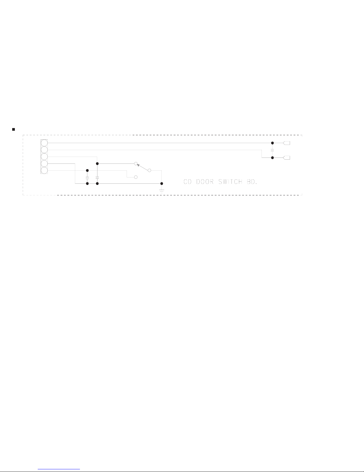
2-10
M-
M+
104
C613
SW2701
102
C614
102
C615
5
OPEN
CN2701
4
3
2
1
GND
CLOSE
M-
M+
To EQUALIZER section CN705
CD DOOR SWITCH section
Page 39

2-11
To EQUALIZER section CN709
10K
R996
1K
R999
0.1uF
C996
P-TU
AMUTE
1K
1K
R711
R709
NC
C740
4.7uF
T7902
0.1uF
C702
NC
D906
NC
R983
1N5819
D701
0.1uF
C701
VC25
220UF
TC701
100K
R701
0.1uF
C703
10K
R708
VCC_3V3
2K5/100MHz
R752
10K
R710
8050
Q906
VCC_3V3
10K
R706
1K
R751
MAINPOWER
VCC_3V3
VC25
CD section 1
CD_TX
CD_RX
VOL+
VOL-
CDPWR
P1_1/ADD4
P1_0/ADD3
P0_7/RXD0/ADD2
P0_6/TXD0/ADD1
P0_4/PINT1_5/ADC2
P0_4/PINT1_4/ADC1
P0_1/PINT11/ADA2
P0_0/PINT10/ADA1
RSTN
P3_3
P3_2
P2_7/TO_CMPA
P1_5/RXOUT
P3_0
P3_1
P1_2/SDA
P1_6/PINT0_0
P1_7/PINT0_1
P0_3/PINT1_3/ADB2
P0_2/PINT1_2/ADB1
VSS
P2_0/XIN
P2_1/XOUT
P2_2/TXD1
P2_3/RXD1
P2_4/T2EX/CMPD
P2_5/T2/CMPC
P2_6/T1/CMPB
9
10
11
12
13
14
15
16
8
7
6
5
4
3
2
1
17
18
19
20
21
22
23
24
CN901
VCC+5V
CD_8V
VCC_3V3
9
8
7
6
5
4
3
2
1
10K
1K
1K
1K
1K
R416
R743
R742
R998
R995
P-USB
PLL_SDA
RDS-RST
RDS-DAT
VCC_3V3
VCC_3V3
EQ_SDA
R970
R971
1K
1K
R745
R744
330
330
4K7
R740
4K7
R741
WP
A2
A1
A0
VCC
GND
SDA
IC701
4
8
7
3
2
1
5
6
IIC_SCL
IIC_SDA
VCC_3V3
103
C998
8050
Q905
10K
R746
U701
1M
R724
20pF
C706
20pF
C705
20pF
C718
OR
R969
3.6864M
X701
OR
R723
32
31
30
29
28
27
26
25
1K
1K
1K
1K
1K
R716
R718
R750
R713
R712
To EQUALIZER section CN407
CN702
24
23
22
21
20
19
18
17
16
15
14
13
12
11
10
4
3
9
8
7
6
5
2
1
P-TU
MAINPOWER
AMUTE
KEY2
IR
KEY1
LCD_RW
LCD_CS
OPEN
CLOSE
OPEN_DET
CLOSE_DET
EQ_SDA
EQ_SCL
PLL_SDA
PLL_SCL
RDS_RST
RDS_RST
PLL_SCL
PLL_SDA
EQ_CSL
EQ_SDA
CLOSE_DET
OPEN_DET
LCD_CS
LCD_RW
KEY1
IR
KEY2
AMUTE
MAINPOWER
P-TU
VOL+
RDS-DAT
100P
68P
C901
C902
68P
68P
68P
C903
C904
C905
102P
102P
100P
C716
C906
C907
100P
103
103
C908
C909
C910
100P
103
100P
C709
C717
C710
100P
100P
100P
C711
C712
C713
103
103
100P
C714
C715
C995
CLOSE_DET
1N4148
D702
OPEN_EDT
CLOSE
OPEN
LCD_CS
LCD_RW
KEY1
1K
1K
1K
1K
1K
1K
1K
2K5/100MHz
R722
R721
R720
R719
R717
R715
R714
R748
AGND
EQ_SCL
IIC_SDA
IIC_SCL
PLL_SCL
DAC_L
DAC_R
18P
C708
32.768K
X702
18P
C707
47K
R968
SCL
P1_3/SCL
P1_4/RXIN
150P
10K
C991
R997
IR
KEY2
1K
330R
R705
R707
VDD
VDD25
LCD_DATA
VOL-
CDPWR
LCD_DATA
LCD_DATA
RDS_DAT
CDPWR
VOLVOL+
To This sheet
To This sheet
To This sheet
To This sheet
To This sheet
To This sheet
To This sheet
To This sheet
Page 40

2-12
15
16
17
18
19
20
213022
23
24
25
26
27
28
CN905
VREF_16
SL-
XSLEGP
MUTE34
SPIN+
SPIN-
VREF_16
10K
R915
47nF
C939
2K5/100MHz
R921
0.47uF
C934
1K
R923
4.7K
NC
R941
R940
5.1K
R945
PGND
PGND
PGND
VREF_16
10uF
C966
0.1uF
C937
DCLOAD+
DCLOAD-
VREF_16
XFOCUS
VREF_16
VREF_16
XTRACK
10nF
C935
R925
10nF
2K5/100MHz
C938
R927
OR
R942
FOCUS+
FOCUS-
TRACK+
TRACK-
NC
R943
PGND
VREF_16
OR
R944
IC903
0.1uF
C936
2R2/0.5W
R470
0.1uF
C943
1000uF
C978
CD+8V
M33V
2K5/100MHz
L913
10R
R935
47uF/16V
C970
GND
3
IC404
OUT
1
PGND
0.1uF
C955
2IN2
470uF
C961
CLOSE_DET
1N4148
D905
100K
R947
M33V
MUTE34
MUTE
P-USB
USB-DET
M33V
CD_TX
CD_RX
10K
10K
R926
R924
100P
C983
100P
C984
M33V_PAD
KEYG2
GND
CD_TX
CD_RX
USB+5V
D+
D-
DGND
4
2
3
1
P_USB
100P
C407
1N4148
D902
30R/100MHz
OR
30R/100MHz
L932
L933
L931
l2C_M_SD
l2S_WCLK
VCC+5V
M33V
0.1uF
C957
2K5/100MHz
L916
V18
2K5/100MHz
L915
V18_CORE
NC
C976
82uF
C921
82uF
C922
3V3SD_IC
V18_CORE
C958
0.1uF
M33V_PAD
0.1uF
C919
R918
R917
10K
10K
10K
R916
AUD_GND
AUD_GND
0.1uF
C924
M33V_CKG
1uF
C917
47uF
C977
0.1uF
C931
16.9344MHz
X901
OR
R934
100K
R936
10uF/10V
C971
GND
30pF
C929
30pF
C925
0.1uF
C926
0.1uF
C918
TELPFO
FELPFO
0.1uF
C914
XTRACK
XSLEGP
XFOCUS
VREF_16
GND
MAPUH
MDPUH
MCPUH
MBPUH
0.1uF
C920
10uF/10V
C969
0.1uF
C927
0.1uF
C911
0.1uF
C912
10uF/10V
C967
HAVC
1
1
1
TELPFO
FELPFO
1N4148
D904
3V3SD_IC
M33V
0.1uF
C960
1uF
C980
10K
R987
4.7K
R984
S8050D
Q901
22K
R986
1N4148
D903
470R
R985
1uF
C979
CD section 2
14
13
12
11
10
9
8
29
7
6
5
4
3
2
1
OUT3-
OUT3+
VDD1
GND
VCC2
BIAS-IN
OUT4+
OUT4-
GND3
OP-OUT
GND2
OUT2-
OUT2+
GND1
GND
MUTE
REG-TR-C
REG-TR-B
2K5/100MHz
1N4001
D410
IN4-A
IN4-B
IN3-B
IN3-A
OP-IN+
OP-IN-
OUT-
OUT+
IN1-A
IN1-B
IN2-B
IN2-A
XSPINDLE
SL+
VC
E
A
C
VCC
D
B
F
VR
F+
T+
LD
MD
T-
F-
1
3
5
7
2
4
6
8
9
11
13
15
10
12
14
16
M33V
M33V_CKG
SEV_3V3
GND
0.1uF
C930
0.1uF
C956
2K5/100MHz
2K5/100MHz
L919
L918
L905
L906
2K5/100MHz
2K5/100MHz
2K5/100MHz
L917
2K5/100MHz
L912
0.1uF
C932
0.1uF
C928
M33V
100uF/10V
C972
2K5/100MHz
L914
AGND
AGND
LD
HAVC
MAPUH
MDPUH
MBPUH
FOCUS+
TRACK+
TRACK-
FOCUS-
33K
33K
R937
R946
M33V
30R/100MHz
L911
R928
100K
5
6
7
8
4
3
2
1
Dl
HOLD#
VCC
GND
DO
CS#
IC902
F_CLK
0.1uF
C954
0.1uF
C990
Reserved for FW
M33V
68P
C987
C985
103
C989
68P
C988
68P
100K
R929
10K
R912
GND
LD
2SB1132/(SOT89)
Q903
MDI
4
3
2
1
5
6
7
8
IC401
C411
104P
C442
104P
C441
100uF/16V
TX
F_CLK
RX
2K5/100MHz
2K5/100MHz
2K5/100MHz
2K5/100MHz
L908
L910
L909
L907
R957
R958
1K
1K
R931
OR
R930
OR
GND
GND
V18_CORE
M33V_PAD
10K
10K
10K
10K
R920
R922
R919
R913
l2S_WCLK
KEYG2
NC
D901
NC
R966
AUD_GND
NC
R991
NC
Q902
NC
Q904
NC
R988
NC
R989
NC
R990
MUTE
AUD_GND
AUD_GND
C962
10uF
C915
0.1uF
C964
1uF
C965
1uF
C968
1uF
C973
1uF
R956
NC
TO CD DECK
GND
GND
C913
0.1uF
C916
0.1uF
M33V_PAD
V18_CORE
1
2
4
3
6
5
SPIN+
SPIN-
SLED+
SLED-
GND
LIMIT1
CN903
AGND
SPIN+
SPIN-
R914
10K
C426
NC
R440
NC
C427
NC
R441
NC
C453
NC
C940
680P
C454
NC
R438
OR
L902
2K5/100MHZ
R938
10K
R948
C974
AUD_GND
R439
OR
L900
2K5/100MHZ
GND
R949
C941
680P
R939
10K
C975
104
103
105
106
107
108
109
111
113
110
112
114
115
116
118
120
117
119
121
122
123
125
127
124
126
128
GPIOI4_PWM1
GPIOI6
GPIOJ2
VDD_PAD
GPIOJ1
GND_CORE
VDD_CORE
BTN_ADIN2
VREF16
BTN_ADIN1
BTN_ADIN3
AVDD33_1
AVSS33_1
38
37
35
33
36
34
32
31
30
29
27
25
28
26
24
23
22
21
20
18
16
19
17
15
14
13
11
9
12
10
8
7
6
4
2
5
3
1
AVDD33_AUD
AVSS33_AUD
BCAPOR
BCAPOL
AVSS18_1
AVDD18_1
AVDD33_CKG
AVSS33_CKG
AVSS33_3
AVDD33_3
COSP
COSN
AVSS33_2
HAVC
TELP
AVDD33_2
MA
MD
MC
TP
MB
TP
LD
63
64
62
61
60
59
58
56
54
57
55
53
52
51
49
47
50
48
46
45
44
42
40
43
41
39
XGPIOC3/URRX
XGPIOD0/I2CM
XGPIOC1/SFSCK
XGPIOC0/SFCSB
GND_PAD
VDD_CORE
VDD_PAD
GND_CORE
DM
SFGN
VREF
V08R
SFGP
V15R
V15L
V08L
MICBIAS
LINEINR
LINEINL
66
65
67
68
70
69
71
72
74
73
75
76
78
77
79
80
81
82
83
85
84
GPIOD1/I2CM_DAT
GPIOD5/I2S_DI
GPIOD4/I2S_D0
GPIOD6/I2S_WCLK
GPIOE4/SDD0
87
86
88
89
90
92
94
91
93
95
96
97
99
101
98
100
102
GPIOE6/SDD2
GPIOE5/SDD1
GPIOE7/SDD3
GPIOF0/SDCMD/MSBS
GPIOF1/SD/MS_CLK
GPIOF2/SD_MS_PWR
GPIOF3/SD_MS_DET
VDD_PAD
GND_PAD
GPIOG4/USI_CLK
GPIOG5/DATA0
GPIOG6/DATA1
GPIOH0/DATA3
GPIOH2/DATA5
GPIOG7/DATA2
GPIOH1/DATA4
GPIOH3/DATA6
GPIOH4/DATA7
GPIOH5/LCDAO
GPIOI0/LCDWPJ
GPIOH6/LCDCSJ
GPIOH7/LCDRDJ
GPIOI1/PWM0
SBLPFO
TP1
TP2
TP3
SEV_3V3
LDO
TPI
TNI
RESETJ
XSPINDLE
MDI
SEV_3V3
1
2
O
SBLPFO
SEV_3V3
M33V_LDO
V18
RF_1V8
LINE_L
LINE_R
AUD_3V3
RF_1V8
V12
MPXOUT1
MPXOUT3
MPXOUT2
VTB
VTP
AVSS33_LDO
AVDD33_LDO
AVDD18_LDO
XTALI
XTAL0
BCAPIL
LINEOUTL
BCAPIR
LINEOUTR
IC901
GPIOG3/USI_DI
GPIOG2/USI_DO
MDI
TRO
FOO
GPWM
DMO
FMO
AVDD_D33
GND_PAD
GPIOJ0/I2S_DAT
GPIOJ0/I2S_CLK
GPIOI5
GPIOI4_PWM2
GPIOI2/IRC
LIMIT
PRSTB
IRC
RESETJ
LINE_R
LINE_L
4.7UF
AUD_GND
4.7UF
3V3SD
4K7
LIMIT
SL-
SL+
C933
C959
0.1uF
0.1uF
4K7
DAC_R
DAC_L
DP
FMINR
MICIN
FMINL
XGPIOB6/SFD0
XGPIOB7/SFDI
XGPIOC2/URTX
GPIOD3/I2S_REFCLK
GPIOD2/I2S_SCLK
GPIOE3/SD_MS_WP
GPIOE2/DOCD_CLK
GPIOE1/DOCD_DATI
GPIOE1/DOCD_DAT0
GPIOD7/SPDIF
DOCD_CLK
DOCD_DATO
SPDIF
AUD_3V3
DOCD_DATO
SPDIF
CN603
To USB section CN601
3V3SD
LDO
TPI
MCPUH
TNI
3V3SD
10P
C986
WP#
CLK
F_DO
F_CS
F_Dl
DOCD_CLK
AMUTE
GND
GND
M33V
M33V
Reserved for FW
BOOT_SEL[0]
WDT_EN
SRAM_REPAIR
l2C_M_SCLK
F_CS
F_Dl
F_D0
AUD_3V3
3V3SD_IC
M33V_PAD
M33V_LDO
To This sheet
To This sheet
To This sheet
To This sheet
To This sheet
To This sheet
To This sheet
To This sheet
To This sheet
To This sheet
To This sheet
To This sheet
To This sheet
To This sheet
To This sheet
To This sheet
To This sheet
To This sheet
To This sheet
To This sheet
To This sheet
To This sheet
To This sheet
To This sheet
To This sheet
Page 41

2-13
D602
D601
GND3
CN601
GND2
C601
C485
JK601
GND5
USB+5V
DD+
GND
V:TA-B
248-TB3038-100
L606
L602
L601
L603
C484
C483
L605
C602
L604
(foward side)
(reverse side)
CN404
FAN+
FAN-
Q410
R420
C411
J2
C412
C1113
IC403
J319
IC404
J304
J308
J307J307
C319
C488
J69
J38
J75
CN302
AUX-R
AUX-GND
AUX-L
J302
TO DISPLAY PCB CN303
ZD402
TO RECTIFER PCB CN1105
C326
DB1102
C339
R417
D304
J54
J55
Q314
Q313
IC303
TO TRANSFOMER
AC18V2
AC18V1
C415
R416
C413
R423
J316
J72
J320
J317
J57
C321
C490
C308
C313
C612
C322
C320
IC402
C727
D302
Q403
C409
R405
J73
D308
R404
R460
GND7
C401
C1112
J34
TO DISPLAY BD.CN301
C340
JK306
D303
C487
D309
L304
L303
L302
L301
D305
D301
JK301
IC401
J60
C407
C403
R401
D1106
D1107
R1105
R1104
ZD403
DB1101
CN1104
J13
C492
D306
C329
C763
D307
C330
ZD406
Q303
J76
C323
ZD405
CN305
PHONE-GND
PHONE-L
PHONE-R
HP-MUTE
CN1101
J66
TO TRANSFONER
IC302
2
1
34
33
CN708
LED+5V
STBY
P-FAN
IR
KEY1
LCD-CS
LCD-RW
LCD-DAT
VOL-
VOL+
MCU 3V3
P-MUTE
MCU-GND
AC3V3
AC3V3
-27V
CN402
+3.3V
+9V
DGND
ECO_CTL
FS1102 T6.3AL 250V
GND6
T
O
D
I
S
P
L
A
Y
P
C
B
C
N
3
0
8
248-TB3002-147
V:TA-B
FS1103 T1.6AL 250V
AC14V
AC14
AC21V
DGND
AC21V
VF1
VF0
VF2
TO EQ PCB JK305
C496
C452
R304
R413
R348
R324
J33
C441
J7
C500
J15
C465
C504
C506
C501
C442
C467
C502
C503
C464
J29
J27
C474
R301
C444
C443
R302
C478
J65
C439
C440
C304
J23
J36
J37
R422
R406
C479
J44
J45
J8
R449
R408
C475
C760
C448
R465
R307
R466
Q309
J51
R309
R451
R321
R452
R456
R308
J52
J35
C497
R310
R394
R402
C436
C477
R403
C406
R462
R392
R343
J41
C453
Q406
J59
C402
C438
J56
R409
R459
C325
J71
R340
Q306
R391
C324
R393
R303
R306
J49
J50
J47
R305
J70
R325
J61
J48
R347
R450
R314
R349
R318
R319
J53
Q308
Q301
R327
R351
Q305
Q304
R332
R320
C306
R342
C331
J40
C328
C454
R328
J42
R336
Q307
J39
C1109
Q302
C493
R311
R464
R463
C455
C1108
C449
C495
C451
C450
R395
C494
R397
R396
C1110
R445
C459
R446
C311
J62
C458
C457
C456
J63
C414
R421
Q409
R419
(foward side)
(reverse side)
Printed circuit boards
MAIN
board
( Lead free solder used in the board (material : Sn-Ag-Cu, melting point : 219 Centigrade) )
USB board
( Lead free solder used in the board (material : Sn-Ag-Cu, melting point : 219 Centigrade) )
Page 42

2-14
DISPLAY
board
( Lead free solder used in the board (material : Sn-Ag-Cu, melting point : 219 Centigrade) )
L307
L308
L306
JK304
L305
TO MAIN PCB CN305
SW707
CN308
HP-MUTE
PH-R
PH-L
GND
POWER
L311
JK302
L310
L309
SW702
ECO
CN301
AUX-R
AUX-GND
AUX-L
TO MAIN PCB CN302
LED702
LED701
248-TB3015-111
V:TA-B
SW711
AUX
SW701
CD
SW715
USB
SW714
TU/BAND
J17
D707
D706
CN303
LED+5V
STBY
P-FAN
IR
KEY1
LCD-CS
LCD-RW
LCD-DAT
VOLVOL+
MCU 3V3
P-MUTE
MCU-GND
AC3V3
AC3V3
-27V
J46
J701
VFD701
R701
IR701
C705
C754
C707
J26
J1
R702
J18
TO VOL BD.CN401
TO MAIN PCB CN708
CN702
VOL+
VOL-GND
VOLLED+5V
LED-GND
C445
R389
R388
Q704
JP23
JP24
JP15
JP38
JP12
JP28
JP3
C756
R761
C753
C706
C704
C755
JP40
JP19
JP29
C709
Q702
JP36
JP27
JP37
R780
C770
Q703
R776
R777
C773
JP39
JP26
JP30
R779
C771
C772
C702
C765
R717
C764
R786
R719
R704
R708
JP35
39
R784
C767
C769
C768
R720
R722
R721
JP32
R785
L704
C758
40
R787
JP703
R718
R788
14
26
27
IC701
C759
52
13
L702
L703
R778
L706
JP31
R773
R774
R711
C733
L701
C730
C731
JP33
C468
R769
Q701
C757
C460
Q710
R390
R382
R380
R764
JP34
R716
R712
C473
C471
C470
C761
R386
C446
R387
C377
C375
C376
R383
R384
(foward side)
(reverse side)
C469
CN1103
C1107
CN1102
250VT2AL
C1106
L1101
PT1101
RL1101
C1104
D1105
D1102
D1103
D1104
C1101
C1102
C1103
CN1105
+3.3V
+9V
DGND
ECO_CTL
TO MAIN PCB CN402
C1114
C1111
D1108
C1105
C1115
D1101
248-TB3012-100
V:TA-B
FS1101
CAUTION:
FOR CONTINUED PROTECTION
AGAINST RISK OF FIRE,
ONLY WITH SAME TYPE FUSE
R1112
JP1102
R1113
R1110
R1109
R1114
Q1103
R1102
C1117
R1108
R1106
Q1102
R1107
R1101
R1111
R1103
IC1101
C1118
C1116
(foward side)
(reverse side)
RECTIFIER
board
( Lead free solder used in the board (material : Sn-Ag-Cu, melting point : 219 Centigrade) )
VOLUME
board
( Lead free solder used in the board (material : Sn-Ag-Cu, melting point : 219 Centigrade) )
CN401
LED-GND
LED+5V
VOLVOL-GND
VOL+
LED401
TO DISPLAY BD. CN701
VR401
LED402
LED403
248-TB3004-100
V:TA-B
C419
C417
R471
R472
R470
C421
C420
C422
C416
C418
(foward side)
(reverse side)
Page 43

2-15
EQUALIZER
board
( Lead free solder used in the board (material : Sn-Ag-Cu, melting point : 219 Centigrade) )
D401
D402
R467
D403
D404
J21
JK305
JK305
MCU-GND
MCU-GND
KEY1
LCD-RW
VOL-
ECO-CTL
USB+5V
TU-GND
CD-GND
CD-GND
CD+8V
VCC+9V
NC
MAIN-L
AUX-R
AGND
AGND
MCU-GND
REMOTE
LCD-CS
LCD-DAT
VOL+
USB+5V
MCU+3V3
TU-GND
P-CD
CD-GND
CD+8V
VCC-MOTO
A-MUTE
MAIN-R
AUX-GND
AUX-L
AGND
C356
C359
C361
C368
C367
C362
34
33
GND1
CN703
DGND
KEY2
J67
J68
J6
C428
TO CD DOOR PCB CN2701]
C611
C762
L510
GND4
1
2
C355
C354
J10
TO MAIN PCB JK301
J31
J30
C351
C352
C357
ZD401
J32
C373
TO CD PCB CN901
CN407
USB_GND
MCU_3V3
CD_8V
MCU_GND
USB_5V
CD_GND
CD_L
CD_AGND
CD_R
J11
J22
J28
J9
TO CD PCB CN702
J5
J4
J20
J19
J14
J3
J74
J12
J16
IC502
ZD404
ZD501
CN705
M+
M-
CLOSE
DGND
OPEN
TO CONTROL PCB CN704
TO TUNER MODE
CN504
TU-RST
PLL-SCL
PLL-SDA
RDS-DAT
TU-VDD
AGND
AGND
TU-R
AGND
TU-L
TU-RST
PLL-SCL
PLL-SDA
IIC-SCL
IIC-SDA
CLOSE-DET
OPEN-DET
CLOSE-DRV
OPEN-DRV
LCD-CS
LCD-RW
LCD-DAT
IR
KEY1
RDS-DAT
KEY2
GND
P-CN
AMUTE
P-TU
P-CD
VOL+
VOL-
CN709
248-TB3010-114
V:TA-B
R379
C390
C393
C392
JP17
C391
JP9
C399
C397
C398
C400
C378
R469
C491
C387
C383
C382
C385
C384
R433
R461
R430
C427
C396
R431
R375
R432
R772
R747
R376
JP2
C430
Q401
C395
JP1
C498
JP4
JP25
R447
R448
Q402
R457
R418
R474
R737
R468
JP10
R429
C489
C394
JP22
R736
R439
R735
R440
JP13
JP18
JP5
JP21
JP20
JP11
C461
C386
C723
C507
C499
C724
C463
C505
C388
C389
R365
R362
JP14
R364
C364
R441
C369
C353
JP6
C358
C610
JP8
C371
L504
R378
R361
JP7
C435
C302
R370
R371
R363
C434
C301
C363
C372
C480
IC301
R369
C433
C431
C432
C600
C360
R368
C365
R366
C366
C374
R367
C370
C481
L503
R442
R443
JP16
(foward side)
(reverse side)
JK101
J104
CF101
V:TA-A
248-TB30001-103
J106
J101
AGND
J102
X101
C120
RST
CN101
VCC
DATA
CLK+
RDS
R OUT
DGND
DGND
J103
L OUT
(foward side)
R108
R109
C111
C112
R107
R131
C109
C119
C110
C118
VP101
D103
C114
C116
R116
R117
R118
R119
C115
C117
C106
R120
1
(reverse side)
C103
R103
R104
R105
C104
C105
R102
C101
C102
IC101
R101
TUNER
board
( Lead free solder used in the board (material : Sn-Ag-Cu, melting point : 219 Centigrade) )
Page 44

2-16
CD
board
( Lead free solder used in the board (material : Sn-Ag-Cu, melting point : 219 Centigrade) )
Q902
R991
R990
C979
R989
Q904
R988
R966
R984
C960
L906
JMP917
C715
R947
R925
C935
R986
R985
JMP916
R914
R921
C942
Q901
R927
C938
C939
R923
R935
L913
C958
R987
R918
R917
R916
R981
C916
JMP915
C911
R937
R932
R946
C914
C917
JMP905
C919
JMP902
JMP906
C933
L912
R934
C928
C918
C927
C924
C925
C921
C922
JMP2
L915
R936
C930
L919
C936
C931
JMP904
L914
C920
C937
JMP907
JMP911
JMP909
R944
C912
C929
L918
JMP912
L916
R941
R945
R942
JMP922
R915
IC903
JMP903
C943
R994
IC404
C934
JMP901
C963
R938
C940
R948
L902
R438
C453
R440
C426
C994
C407
JMP908
JMP920
IC401
R939
C427
C993
R949
C941
L900
C454
R439
R441
C411
C442
C968
C973
C964
C965
L917
C932
R956
L945
L944
L932
L931
C988
L908
C989
R992
R982
R928
C990
C986
C985
JMP913
C987
JMP914
L910
IC902
L933
R924
R926
R931
C915
R930
C956
L907
R718
R716
L909
R929
L911
C718
C954
Q905
C998
JMP921
JMP910
R724
C706
C997
C984
C983
C959
IC901
U701
R723
R958
C957
R957
R922
R993
C705
R999
C913
L905
R920
R919
R912
R969
C714
C713
C712
C711
C710
C709
C910
C909
C908
C907
C906
C905
C904
C903
C902
C901
C995
R742
R744
R995
R968
R739
R416
R715
C707
R997
R707
R705
C703
R719
R720
R721
R717
JMP704
C702
C716
Q906
R706
C717
R701
R710
R708
R913
R752
R996
C991
R741
R740
R714
R748
R722
IC701
R753
R970
R750
R713
R712
R711
R751
R709
R971
R743
R745
C708
JMP1
JMP703
C701
R746
R998
JMP701
JMP702
248-TB3009-173
J914
T7902
C992
+
5V
TO EQ BD.CN407
TO EUSB BD.CN601
C999
GND
LOUT
J909
J902
J903
J904
ROUT
J905
AGND
USB +5V
DD+
GND
CN603
D902
C441
D701
X701
TC701
J901
J906
C996
C978
CD_GND
MCU+3V3
CD+8V
GND
D410
CN901
L901
R470
HOME-SW
CN907
TO CD DECK
SP-
SP+
SL+
SL-
DGND
J910
C974
C975
J911
C962
C976
X901
C961
C977
C971
TO EQ BD.CN704
GND
CLOSE_DET
OPEN_DET
LCD-DATA
CLOSE
llC_SCL
RDS_RST
PLL_SCL
PLL_SDA
llC_SDA
KEY1
OPEN
LCD-CS
LCD-RW
KEY2
RDS-DAT
IR
C970
CN702
C980
CDPWR
AMUTE
MAINPWR
PPWR
VOL-
VOL+
VREF
C967
FOCUS-
C969
FOCUS-
TRACK+
TRACK-
C966
BB
CN905
MDI
VR
LD
GND
F
C
B
A
D
E
VCC
C972
TO CD DECK
Q903
V:TA-B
D702
X702
J913
J912
D905
J907
J908
D903
D901
B
D904
(foward side)
(reverse side)
CN2701
M+
MCLOSE
DGND
OPEN
248-TB3027-100
V:TA-B
SW2701
C613
C615
C614
M+
M-
(foward side)
(reverse side)
SW717
STOP
SW716
PLAY
CN704
KEY2
DGND
SW720
OPEN/CLOSE
TO EQ PCB CN703
248-TB3003-100
V:TA-B
SW719
PRESET+
SW718
PRESET-
SW713
TU-UP
SW712
TU-DN
R767
R770
R768
R765
R771
R762
L705
C751
R775
(foward side)
(reverse side)
CONTROL
board
( Lead free solder used in the board (material : Sn-Ag-Cu, melting point : 219 Centigrade) )
CD DOOR SWITCH
board
( Lead free solder used in the board (material : Sn-Ag-Cu, melting point : 219 Centigrade) )
Page 45

< MEMO >
Page 46

Victor Company of Japan, Limited
Home Entertainment Business Division Personal AV Operation
(No.MB725SCH<Rev.001>)
Printed in Japan
VSE
 Loading...