

Page 1
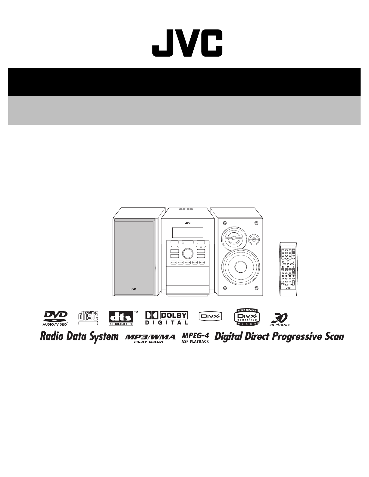
SERVICE MANUAL
MICRO COMPONENT SYSTEM
MB50520066
UX-G70J,UX-G70C,UX-G70B,
UX-G70E,UX-G70EN,
UX-G70EV,UX-G70EE
CA-UXG70
SUPER VIDEO
Lead free solder used in the board (material : Sn-Ag-Cu, melting point : 219 Centigrade)
TABLE OF CONTENTS
1 PRECAUTION. . . . . . . . . . . . . . . . . . . . . . . . . . . . . . . . . . . . . . . . . . . . . . . . . . . . . . . . . . . . . . . . . . . . . . . . . 1-3
2 SPECIFIC SERVICE INSTRUCTIONS . . . . . . . . . . . . . . . . . . . . . . . . . . . . . . . . . . . . . . . . . . . . . . . . . . . . . . 1-8
3 DISASSEMBLY . . . . . . . . . . . . . . . . . . . . . . . . . . . . . . . . . . . . . . . . . . . . . . . . . . . . . . . . . . . . . . . . . . . . . . . 1-9
4 ADJUSTMENT . . . . . . . . . . . . . . . . . . . . . . . . . . . . . . . . . . . . . . . . . . . . . . . . . . . . . . . . . . . . . . . . . . . . . . . 1-32
5 TROUBLESHOOTING . . . . . . . . . . . . . . . . . . . . . . . . . . . . . . . . . . . . . . . . . . . . . . . . . . . . . . . . . . . . . . . . . 1-37
COPYRIGHT © 2006 Victor Company of Japan, Limited
SP-UXG70SP-UXG70
No.MB505
2006/6
Page 2
SPECIFICATION
Amplifier section Output Power Northern america 120 W per channel, min. RMS, driven into 6 Ω at 1kHz with no more than 10% total
harmonic distortion. (for northern america)
Europe 160 W (80 W+80 W) at 6
Audio Input LINE IN 500 mV/49 k
250 mV/49 k
125 mV/49 k
GAME IN (northern america) 500 mV/49 k
TV SOUND IN 500 mV/49 kΩ
Audio Output LINE OUT 1.0 Vrms (3 kΩ) (at "L.OUT LVL1")
SUBWOOFER OUT 260 mVrms/3.9 k
HEADPHONES OUT 17 mW/32 Ω
Digital output DVD OPTICAL DIGITAL OUT -21 dBm to -15 dBm (660 nm ±30 nm)
USB input USB AUDIO
Video Output Color system NTSC (interlaced/progressive) for northern america
VIDEO (composite) 1 V(p-p)/75
S-VIDEO Y (luminance) : 1 V(p-p)/75 Ω
RGB 0.7 V(p-p)/75
COMPONENT (Y) : 1 V(p-p)/75
Speaker impedance 6
Headphone impedance 16 Ω - 1 kΩ
Tuner section FM tuning range 87.5 MHz - 108.0 MHz
AM tuning range 530 kHz - 1 710 kHz for northern america
Disc player section Playable disc DVD Video/DVD Audio/CD/VCD/SVCD
Dynamic range 80 dB
Horizontal resolution 500 lines
Wow and flutter Immeasurable
General Power requirement AC 120 V , 60 Hz for northern america
Power consumption 90 W (at operation) for northern america
Dimensions (approx.)(W/H/D) 175 mm
Speakers Speaker units Tweeter 1.5 cm (5/8 inch) dome
Squawker 4 cm (1-5/8 inch) cone
Woofer 13.5 cm (5-3/8 inch) cone
Impedance 6
Dimensions (approx.) (W/H/D) 166 mm × 250 mm × 232 mm (6-9/16 inch × 9-7/8 inch × 9-3/16 inch)
Mass (approx.) 2.8 kg (6.2 lbs) each
500 mVrms (1.5 k
PAL (interlaced/progressive) for europe
C (chrominance, burst) : 0.286 V(p-p)/75 Ω for northern america
C (chrominance, burst) : 0.3 V(p-p)/75
(PB/PR) : 0.75 V(p-p)/75 Ω for northern america
(PB/PR) : 0.7 V(p-p)/75
Ω - 16 Ω
522 kHz - 1 629 kHz fro europe
CD-R/CD-RW (CD/SVCD/VCD/MP3/WMA/JPEG format)
DVD-R/-RW (DVD-VR/DVD Video/MP3/WMA/JPEG format)
+R/+RW (DVD Video format)
DVD-ROM (DVD Video format)
AC 230 V , 50 Hz for europe
95 W (at operation) for europe
14 W (at standby)
1.0 W (at standby display OFF mode)
Ω
Ω (at "L.IN LVL1")
Ω (at "L.IN LVL2")
Ω (at "L.IN LVL3")
Ω
Ω
Ω for europe
Ω
× 250 mm × 411 mm (6-9/10 inch × 9-7/8 inch × 16-1/5 inch)
Ω (10% THD) for europe
Ω) (at "L.OUT LVL2")
Ω
Ω for europe
Ω for europe
× 1
× 1
× 1
Design and specifications are subject to change without notice.
1-2 (No.MB505)
Page 3
SECTION 1
PRECAUTION
1.1 Safety Precautions
(1) This design of this product contains special hardware and
many circuits and components specially for safety purposes. For continued protection, no changes should be made
to the original design unless authorized in writing by the
manufacturer. Replacement parts must be identical to
those used in the original circuits. Services should be performed by qualified personnel only.
(2) Alterations of the design or circuitry of the product should
not be made. Any design alterations of the product should
not be made. Any design alterations or additions will void
the manufacturers warranty and will further relieve the
manufacture of responsibility for personal injury or property
damage resulting therefrom.
(3) Many electrical and mechanical parts in the products have
special safety-related characteristics. These characteristics are often not evident from visual inspection nor can the
protection afforded by them necessarily be obtained by using replacement components rated for higher voltage, wattage, etc. Replacement parts which have these special
safety characteristics are identified in the Parts List of Service Manual. Electrical components having such features
are identified by shading on the schematics and by ( ) on
the Parts List in the Service Manual. The use of a substitute
replacement which does not have the same safety characteristics as the recommended replacement parts shown in
the Parts List of Service Manual may create shock, fire, or
other hazards.
(4) The leads in the products are routed and dressed with ties,
clamps, tubings, barriers and the like to be separated from
live parts, high temperature parts, moving parts and/or
sharp edges for the prevention of electric shock and fire
hazard. When service is required, the original lead routing
and dress should be observed, and it should be confirmed
that they have been returned to normal, after reassembling.
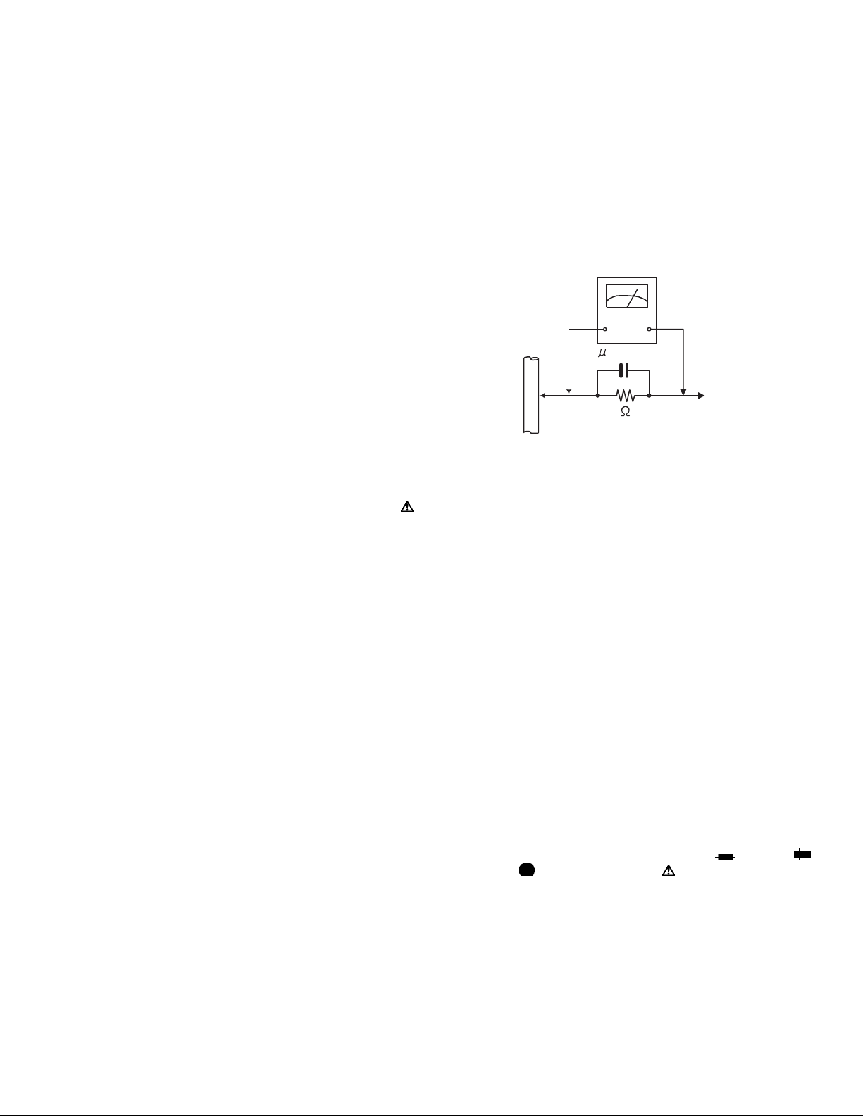
(5) Leakage shock hazard testing
After reassembling the product, always perform an isolation check on the exposed metal parts of the product (antenna terminals, knobs, metal cabinet, screw heads,
headphone jack, control shafts, etc.) to be sure the product
is safe to operate without danger of electrical shock.Do not
use a line isolation transformer during this check.
• Plug the AC line cord directly into the AC outlet. Using a
"Leakage Current Tester", measure the leakage current
from each exposed metal parts of the cabinet, particularly any exposed metal part having a return path to the
chassis, to a known good earth ground. Any leakage current must not exceed 0.5mA AC (r.m.s.).
• Alternate check method
Plug the AC line cord directly into the AC outlet. Use an
AC voltmeter having, 1,000Ω per volt or more sensitivity
in the following manner. Connect a 1,500Ω 10W resistor
paralleled by a 0.15µF AC-type capacitor between an ex-
posed metal part and a known good earth ground.
Measure the AC voltage across the resistor with the AC
voltmeter.
Move the resistor connection to each exposed metal
part, particularly any exposed metal part having a return
path to the chassis, and measure the AC voltage across
the resistor. Now, reverse the plug in the AC outlet and
repeat each measurement. Voltage measured any must
not exceed 0.75 V AC (r.m.s.). This corresponds to 0.5
mA AC (r.m.s.).
AC VOLTMETER
(Having 1000
ohms/volts,
or more sensitivity)
0.15 F AC TYPE
Place this
probe on
1500 10W
Good earth ground
1.2 Warning
(1) This equipment has been designed and manufactured to
meet international safety standards.
(2) It is the legal responsibility of the repairer to ensure that
these safety standards are maintained.
(3) Repairs must be made in accordance with the relevant
safety standards.
(4) It is essential that safety critical components are replaced
by approved parts.
(5) If mains voltage selector is provided, check setting for local
voltage.
1.3 Caution
Burrs formed during molding may be left over on some parts
of the chassis.
Therefore, pay attention to such burrs in the case of preforming repair of this system.
1.4 Critical parts for safety
In regard with component parts appearing on the silk-screen
printed side (parts side) of the PWB diagrams, the parts that are
printed over with black such as the resistor ( ), diode ( )
and ICP ( ) or identified by the " " mark nearby are critical
for safety. When replacing them, be sure to use the parts of the
same type and rating as specified by the manufacturer.
(This regulation dose not Except the J and C version)
each exposed
metal part.
(No.MB505)1-3
Page 4
1.5 Safety Precautions (U.K only)
(1) This design of this product contains special hardware and many circuits and components specially for safety purposes. For con-
tinued protection, no changes should be made to the original design unless authorized in writing by the manufacturer. Replacement parts must be identical to those used in the original circuits.
(2) Any unauthorised design alterations or additions will void the manufacturer's guarantee; furthermore the manufacturer cannot
accept responsibility for personal injury or property damage resulting therefrom.
(3) Essential safety critical components are identified by ( ) on the Parts List and by shading on the schematics, and must never
be replaced by parts other than those listed in the manual. Please note however that many electrical and mechanical parts in
the product have special safety related characteristics. These characteristics are often not evident from visual inspection. Parts
other than specified by the manufacturer may not have the same safety characteristics as the recommended replacement parts
shown in the Parts List of the Service Manual and may create shock, fire, or other hazards.
(4) The leads in the products are routed and dressed with ties, clamps, tubings, barriers and the like to be separated from live parts,
high temperature parts, moving parts and/or sharp edges for the prevention of electric shock and fire hazard. When service is
required, the original lead routing and dress should be observed, and it should be confirmed that they have been returned to
normal, after re-assembling.
1.5.1 Warning
(1) Service should be performed by qualified personnel only.
(2) This equipment has been designed and manufactured to meet international safety standards.
(3) It is the legal responsibility of the repairer to ensure that these safety standards are maintained.
(4) Repairs must be made in accordance with the relevant safety standards.
(5) It is essential that safety critical components are replaced by approved parts.
(6) If mains voltage selector is provided, check setting for local voltage.
Burrs formed during molding may be left over on some parts of the chassis. Therefore,
pay attention to such burrs in the case of preforming repair of this system.
1-4 (No.MB505)
Page 5
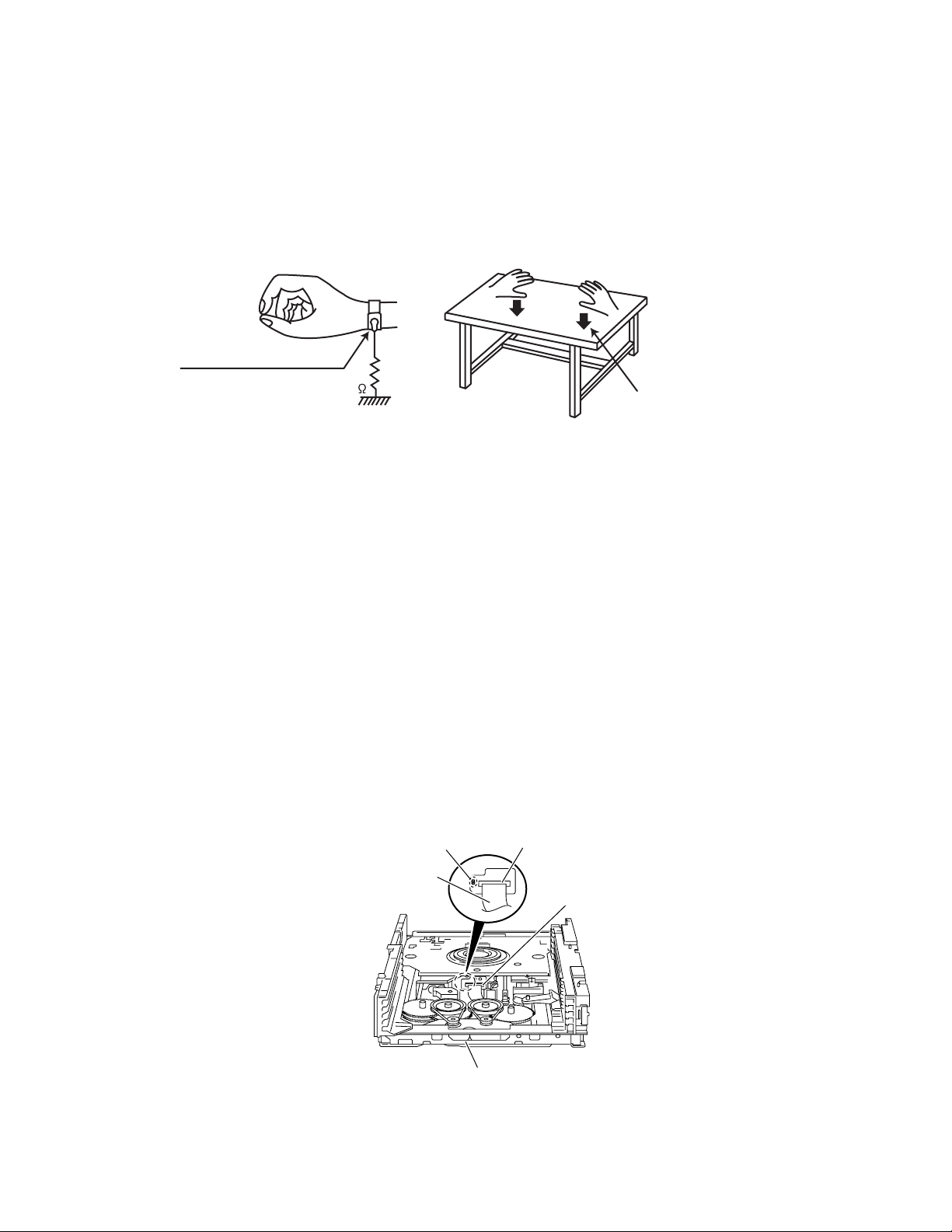
1.6 Preventing static electricity
Electrostatic discharge (ESD), which occurs when static electricity stored in the body, fabric, etc. is discharged, can destroy the laser
diode in the traverse unit (optical pickup). Take care to prevent this when performing repairs.
1.6.1 Grounding to prevent damage by static electricity
Static electricity in the work area can destroy the optical pickup (laser diode) in devices such as laser products.
Be careful to use proper grounding in the area where repairs are being performed.
(1) Ground the workbench
Ground the workbench by laying conductive material (such as a conductive sheet) or an iron plate over it before placing the
traverse unit (optical pickup) on it.
(2) Ground yourself
Use an anti-static wrist strap to release any static electricity built up in your body.
(caption)
Anti-static wrist strap
1M
Conductive material
(conductive sheet) or iron palate
(3) Handling the optical pickup
• In order to maintain quality during transport and before installation, both sides of the laser diode on the replacement optical
pickup are shorted. After replacement, return the shorted parts to their original condition.
(Refer to the text.)
• Do not use a tester to check the condition of the laser diode in the optical pickup. The tester's internal power source can easily
destroy the laser diode.
1.7 Handling the traverse unit (optical pickup)
(1) Do not subject the traverse unit (optical pickup) to strong shocks, as it is a sensitive, complex unit.
(2) Cut off the shorted part of the flexible cable using nippers, etc. after replacing the optical pickup. For specific details, refer to the
replacement procedure in the text. Remove the anti-static pin when replacing the traverse unit. Be careful not to take too long a
time when attaching it to the connector.
(3) Handle the flexible cable carefully as it may break when subjected to strong force.
(4) I t is not possible to adjust the semi-fixed resistor that adjusts the laser power. Do not turn it.
1.8 Attention when traverse unit is decomposed
*Please refer to "Disassembly method" in the text for the pickup unit.
• Apply solder to the short land sections before the card wire is disconnected from the connecto on the servo board. (If the card wire
is disconnected without applying solder, the pickup may be destroyed by static electricity.)
• In the assembly, be sure to remove solder from the short land sections after connecting the card wire.
Short land section
Connector
Card wire
DVD pickup
DVD changer mechanism assembly
(No.MB505)1-5
Page 6
1.9 Importance administering point on the safety
D9044
D9047
D9043
Q9044
IC901
B9105
D9048
C9041
B9301
B9302
B9300
B9104
HS902
C9045
B9106
D9040
B9501
B9600
B9502
D9025
B9202
D9024
D9023
C9022
CN901
HS901
R9046
R9045
C9042
D9042
R9044
FT913
D9004
D9003
C9003
C9024
B9204
C9004
C9023
C9025
C9021
D9022
D9014
D9021
B9900
D9046
D9045
Q9043
FT914
B9203
D9002
D9001
C9005
C9014
D9012
D9011
D9013
B9303
B9205
C9012
R9031
D9031
B9101
RY901
B9102
B9103
C9043
C9044
C9002
FT907
C9001
FT905
C9015
FT909
C9011
FT911
C9013
R9033
R9032
D9032
Q9031
C9031
T9000
FT908
FT906
FT910
FT912
CN903
B9100
B9700
LF901
FT903
FT904
C9052
C9051
B9305
B9304
CN906
R9050
EP901
B9201
B9200
CN904
FT901
FT902
B9500
B9950
CN905
S9001
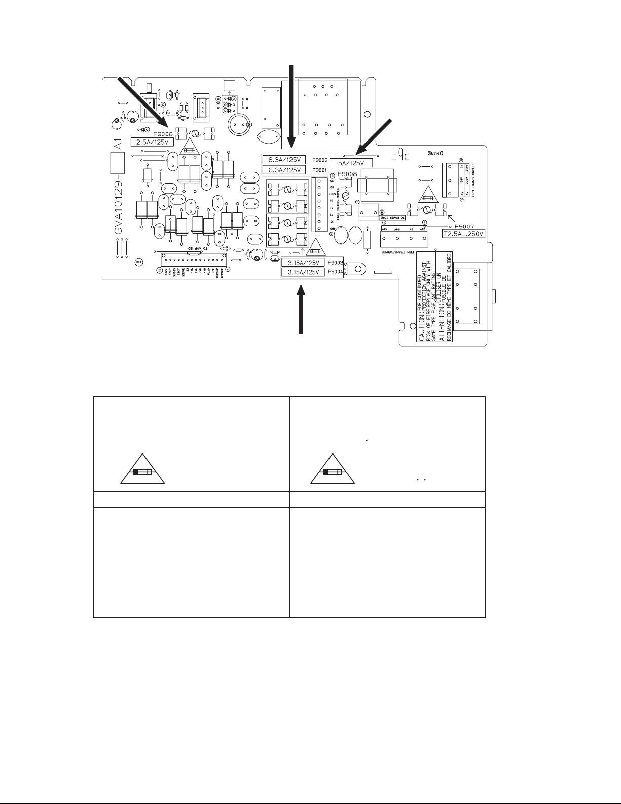
Full Fuse Replacement Marking
Graphic symbol mark
(This symbol means fast blow type fuse.)
should be read as follows ;
FUSE CAUTION
FOR CONTINUED PROTECTION AGAINST RISK
OF FIRE, REPLACE ONLY WITH SAME TYPE
AND RATING OF FUSES ;
F9001 : 6.3A 125V
F9002 : 6.3A 125V
F9003 : 3.15A 125V
F9004 : 3.15A 125V
F9006 : 2.5A 125V
Marquage Pour Le Remplacement
Complet De Fusible
Le symbole graphique (Ce symbole signifie
fusible de type a fusion rapide.)
^
doit etre interprete comme suit ;
PRECAUTIONS SUR LES FUSIBLES
POUR UNE PROTECTION CONTINUE CONTRE
DES RISQUES D'INCENDIE, REMPLACER
SEULEMENT PAR UN FUSIBLE DU MEME TYPE ;
F9001 : 6.3A 125V
F9002 : 6.3A 125V
F9003 : 3.15A 125V
F9004 : 3.15A 125V
F9006 : 2.5A 125V
1-6 (No.MB505)
Page 7
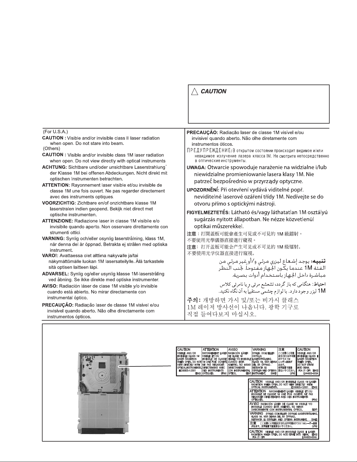
1.10 Important for laser products
1.CLASS 1 LASER PRODUCT
2.CAUTION :
(For U.S.A.) Visible and/or invisible class II laser radiation
when open. Do not stare into beam.
(Others) Visible and/or invisible class 1M laser radiation
when open. Do not view directly with optical instruments.
3.CAUTION : Visible and/or invisible laser radiation when
open and inter lock failed or defeated. Avoid direct
exposure to beam.
4.CAUTION : This laser product uses visible and/or invisible
laser radiation and is equipped with safety switches which
prevent emission of radiation when the drawer is open and
the safety interlocks have failed or are defeated. It is
dangerous to defeat the safety switches.
5.CAUTION : If safety switches malfunction, the laser is able
to function.
6.CAUTION : Use of controls, adjustments or performance of
procedures other than those specified here in may result in
hazardous radiation exposure.
!
Please use enough caution not to
see the beam directly or touch it
in case of an adjustment or operation
check.
REPRODUCTION AND POSITION OF LABELS and PRINT
WARNING LABEL and PRINT
(No.MB505)1-7
Page 8

SECTION 2
SPECIFIC SERVICE INSTRUCTIONS
This service manual does not describe SPECIFIC SERVICE INSTRUCTIONS.
1-8 (No.MB505)
Page 9
SECTION 3
A
DISASSEMBLY
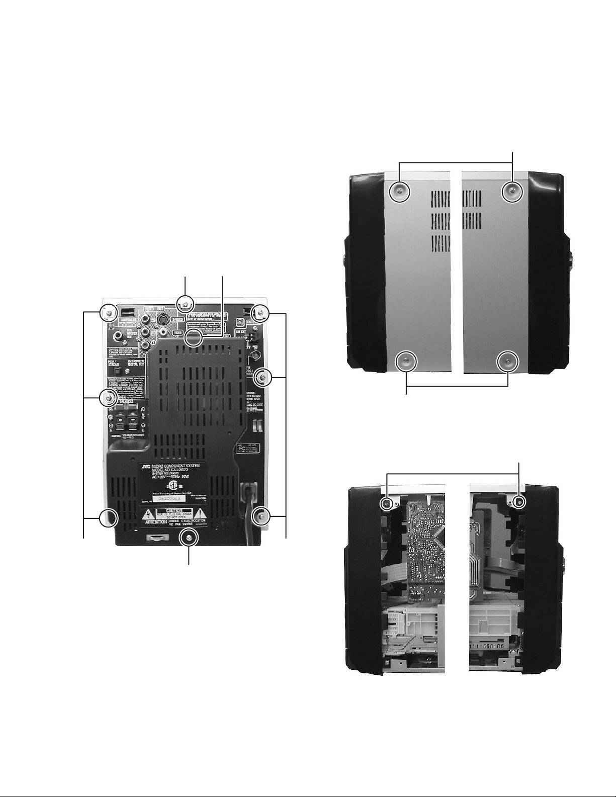
3.1 Main body
3.1.1 Removing the side panel
(Fig.1, 2)
(1) Remove the six screws A attaching the side panel. (See
Fig.1)
(2) Remove the four screws B attaching the side panel. (See
Fig.2)
3.1.2 Removing the top cover
(Fig.1, 3)
(1) Remove the one screw C attaching the top cover. (See
Fig.1)
(2) Remove the two screws D attaching the top cover. (See
Fig.3)
C G
B
G
Fig.1
B
Fig.2
D
A
Fig.3
(No.MB505)1-9
Page 10
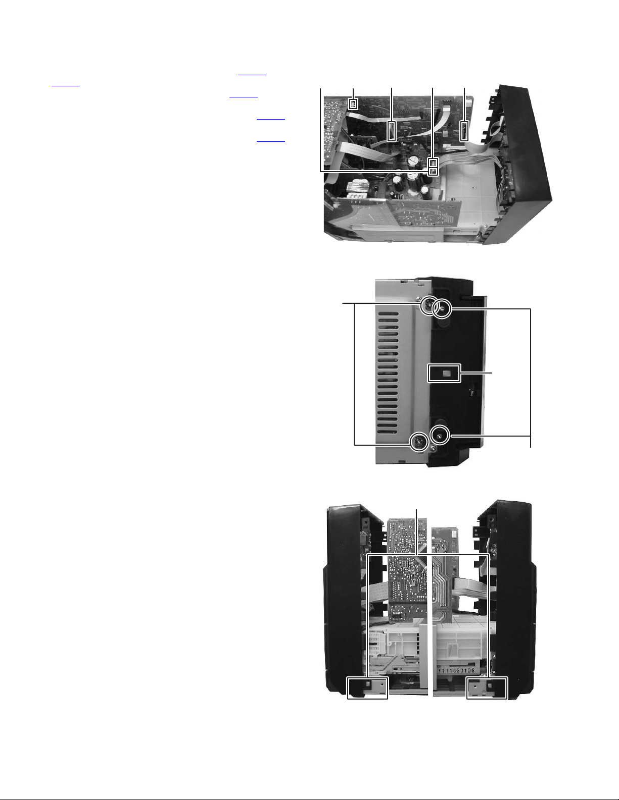
3.1.3 Removing the front panel
(Fig.4 to 6)
(1) Disconnect the card wire from the connector CN359
on the regulator board. (See the Fig.4)
CN360
(2) Disconnect the card wire from the connector CN760 on the
main board. (See Fig.4)
(3) Disconnect the connector wire from the connector CN713
on the main board. (See Fig.4)
(4) Disconnect the connector wire from the connector CN405
on the video board. (See Fig.4)
(5) Remove the two screws E and two screws F attaching the
front panel. (See Fig.5)
(6) Remove the hook a. (See Fig.5)
(7) Remove the hook b and then removing the front panel.
(See Fig.6)
and
CN360
E
CN359
Fig.4
CN706CN713CN405
Fig.5
hook b
hook a
F
3.1.4 Removing the rear cover
(Fig.1)
(1) Remove the two screws G attaching the rear cover.
1-10 (No.MB505)
Fig.6
Page 11
3.1.5 Removing the video board
(Fig.7, 8)
(1) Disconnect the card wire from the connector CN401
on the video board. (See Fig.7)
CN402
(2) Remove the three screws H attaching the video board.
(See Fig.8)
3.1.6 Removing the tuner pack
(Fig.8, 9)
(1) Disconnect the card wire from the connector CN712
main board. (See Fig.9)
(2) Remove the two screws J attaching the tuner pack. (See
Fig.8)
3.1.7 Removing the fan
(Fig.8, 9)
(1) Disconnect the connector wire from the connector CN708
on the main board. (See Fig.9)
(2) Remove the two screws K attaching the fan. (See Fig.8)
on the
and
CN401
CN402
Fig.7
H
J
H
CN712
K
Fig.8
CN708
Fig.9
(No.MB505)1-11
Page 12
3.1.8 Removing the rear panel
(Fig.10, 11)
(1) Remove the eight screws L attaching the rear panel. (See
Fig.10)
(2) Remove the rear panel from the hook c. (See Fig.11)
L
L
L
L
Fig.10
1-12 (No.MB505)
hook c
Fig.11
Page 13
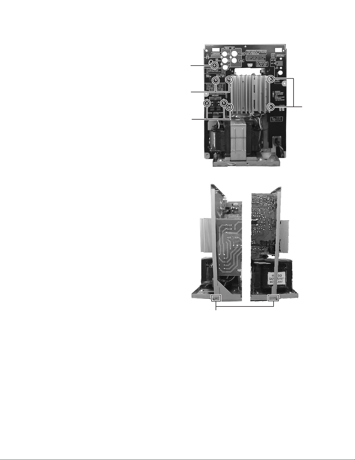
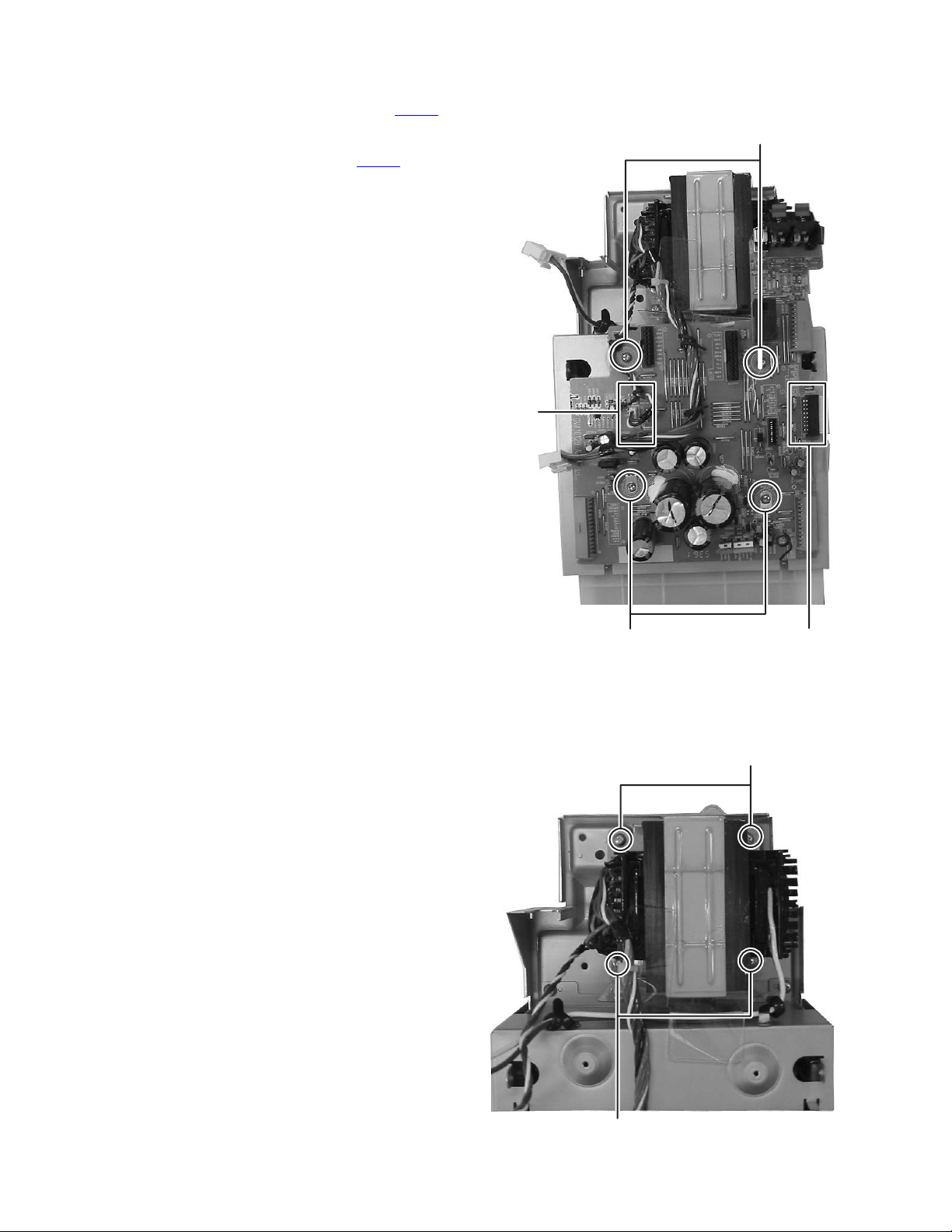
3.1.9 Removing the transformer board
(Fig.12)
(1) Disconnect the connector wire from the connector CN903
on the transformer board.
(2) Remove the one screw M attaching the transformer board.
(3) Disconnect the connector CN901
board and then removing the transformer board with power
cord.
connecting the regulator
3.1.10 Removing the main board
(Fig.13)
(1) Disconnect the card wire from the connector CN703
main board.
(2) Remove the one screw N attaching the main board.
(3) Disconnect the main board from the connector CN701
connecting the regulator board.
CN702
3.1.11 Removing the amplifier board
(Fig.14)
(1) Disconnect the amplifier board from the connector CN353
and CN354.
on the
and
CN904
CN703
M
Fig.12
CN702
Fig.13
CN903 CN901
CN701
N
CN354
CN353
Fig.14
(No.MB505)1-13
Page 14
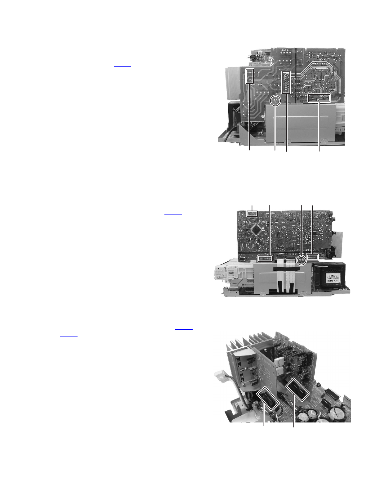
3.1.12 Removing the regulator board
(Fig.15)
(1) Disconnect the connector wire from the connector CN361
on the regulator board.
(2) Remove the four screws P attaching the regulator board.
(3) Disconnect the card wire from the connector CN356
P
.
CN361
3.1.13 Removing the power transformer
(Fig.16)
(1) Remove the four screws Q attaching the power transform-
er.
P
CN356
Fig.15
Q
1-14 (No.MB505)
Q
Fig.16
Page 15
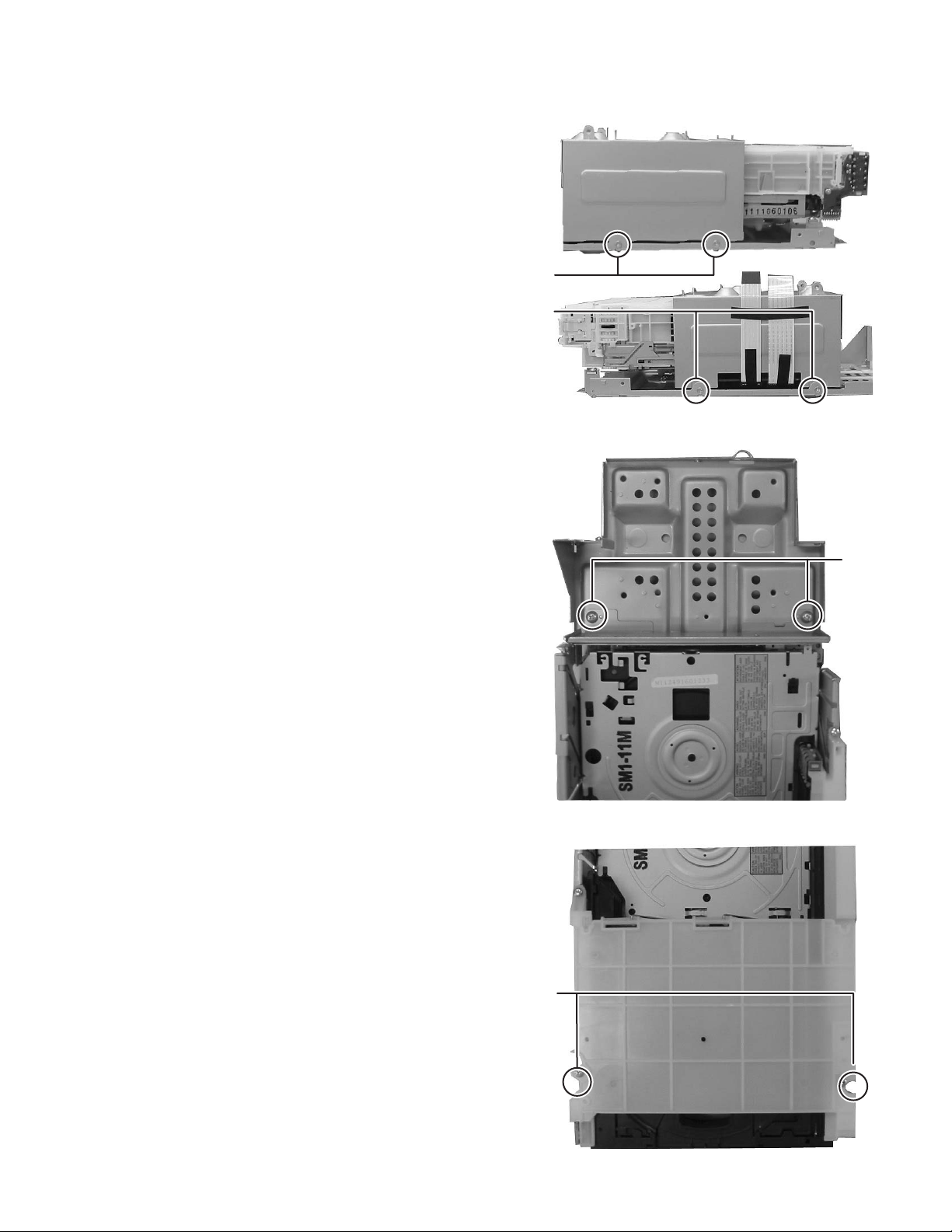
3.1.14 Removing the DVD changer mechanism assembly
(Fig.17 to 19)
(1) Remove the four screws R attaching the main chassis.
(See Fig.17)
(2) Remove the two screws S and two screws T attaching the
DVD changer mechanism assembly. (See Fig.18, 19)
R
R
Fig.17
T
s
Fig.18
Fig.19
(No.MB505)1-15
Page 16
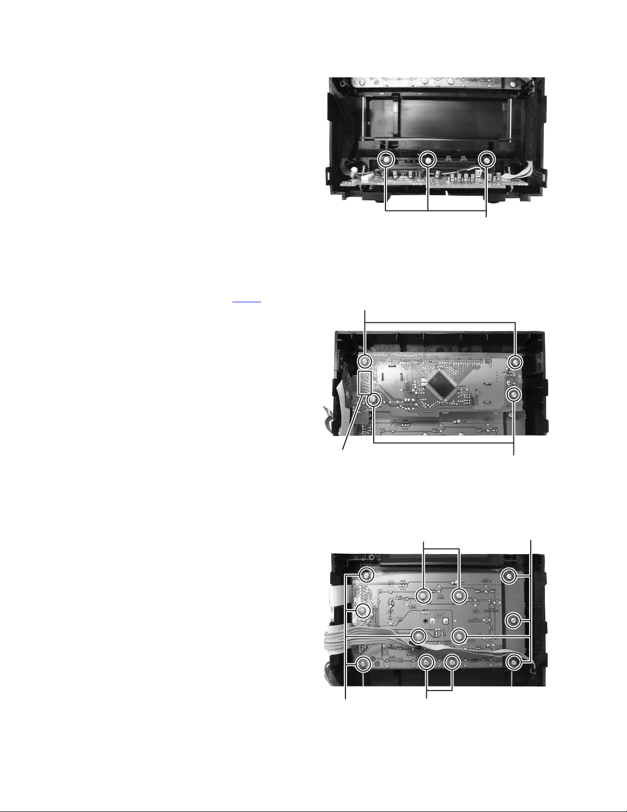
3.1.15 Removing the USB board
(Fig.20)
(1) Remove the three screws U attaching the USB board.
3.1.16 Removing the FL board
(Fig.21)
(1) Remove the four screws V attaching the FL board.
(2) Disconnect the card wire from the connector CN100
FL board.
on the
U
Fig.20
V
3.1.17 Removing the switch board
(Fig.22)
(1) Remove the volume knob.
(2) Remove the twelve screws W attaching the switch board.
CN100
W
Fig.21
W
W
Fig.22
V
W
1-16 (No.MB505)
Page 17
3.2 DVD changer mechanism assembly section
Remove the DVD changer mechanism assembly from the main body. (See "Removing the DVD changer mechanism assembly".)
3.2.1 Removing the tray assemblies
(See Figs.1 to 5)
(1) From the top side of the main body, remove the two screws
A from the top cover and release the two joints a on the
both sides of the DVD changer mechanism assembly. (See
Figs.1 and 2.)
(2) Remove the two rods from the top cover and remove the
top cover from the lifter assembly. (See Figs.1 and 2.)
(3) Remove the open det. lever on the left side of the DVD
changer mechanism assembly. (See Fig.3.)
(4) From the right side of the DVD changer mechanism as-
sembly, draw out the tray assemblies toward the front while
pushing the part b of the side (R) assembly. (See Figs.4
and 5.)
Note:
The tray can be locked if all tray assemblies are attached.
(5) From the topside of the DVD changer mechanism assem-
bly, move the stopper tabs c in the direction of the arrow
and release them. Pull out the tray assemblies from the
DVD changer mechanism assembly. (See Fig. 5.)
Note:
Remove the tray assembly from top tray 5 in order.
Reference:
When reattaching the tray assembly, or when removing the
disc remaining inside, refer to another section "3.3.15 Taking
out the disc in the play mode".
A
a
Lifter assembly
Fig.1
Rods
Top cover
A
a
Rods
Top cover
a
a
Lifter assembly
Fig.2
(No.MB505)1-17
Page 18
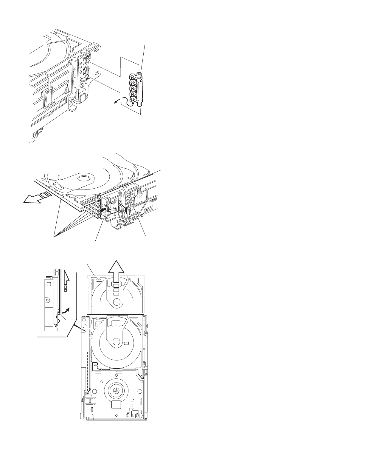
Fig.3
r
Open det. leve
Tray assemblies
c
b
Side(R) assembly
Fig.4
Tray assembly
1-18 (No.MB505)
Fig.5
Page 19
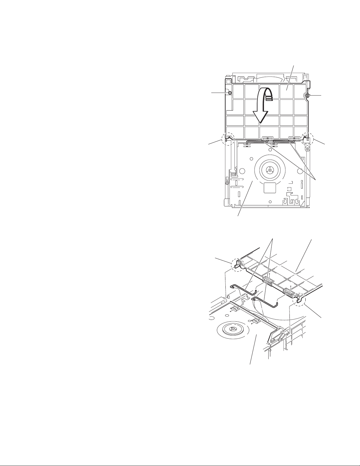
3.2.2 Removing the DVD servo board
(See Figs.6 to 8)
Caution:
Solder the short land sections d on the DVD pickup before disconnecting the card wire extending from the DVD pickup. If
you do not follow this instruction, the DVD pickup may be damaged.
(1) From the topside of the DVD changer mechanism assem-
bly, solder the short land sections d on the DVD pick up.
(See Fig.6.)
(2) From the bottom side of the DVD changer mechanism as-
sembly, disconnect the card wire from the connectors
(CN201
Reference:
(3) Disconnect the wires from the connectors (CN452
on the DVD servo board. (See Fig.7.)
(4) Remove the two screws B attaching the DVD servo board.
(See Fig.7.)
(5) From the reverse side of the DVD servo board, release the
lock of the connector CN101
and disconnect the card wire. (See Fig.8.)
Caution:
Unsolder the solders from the short land sections d after reassembling. (See Fig.6.)
3.2.3 Removing the switch board
(1) From the bottom side of the DVD changer mechanism as-
sembly, remove the screw C attaching the switch board on
the DVD changer mechanism assembly.
(2) Disconnect the wires from the connectors (CN452
on the DVD servo board.
(3) Release the wires from the section f and remove the switch
board.
(4) Release the wires from the sections g and remove the
switch board.
Reference:
When reassembling, pass the wires through the sections (f, g)
as before.
, CN451) on the DVD servo board. (See Fig.7.)
When connecting the card wire to the connector CN451
pass it through the sections e on the DVD traverse
mechanism assembly. (See Fig.7.)
, CN453)
in the direction of the arrow
(See Fig.7)
, CN453)
d
,
DVD changer mechanism assembly
Fig.6
DVD changer mechanism assembly
e
CN451
DVD pickup
CN453
f
g
Switch board
B
C
CN201
DVD servo board
DVD traverse mechanism assembly
DVD servo board
B
Fig.7
CN452
CN101
Fig.8
Lock
(No.MB505)1-19
Page 20
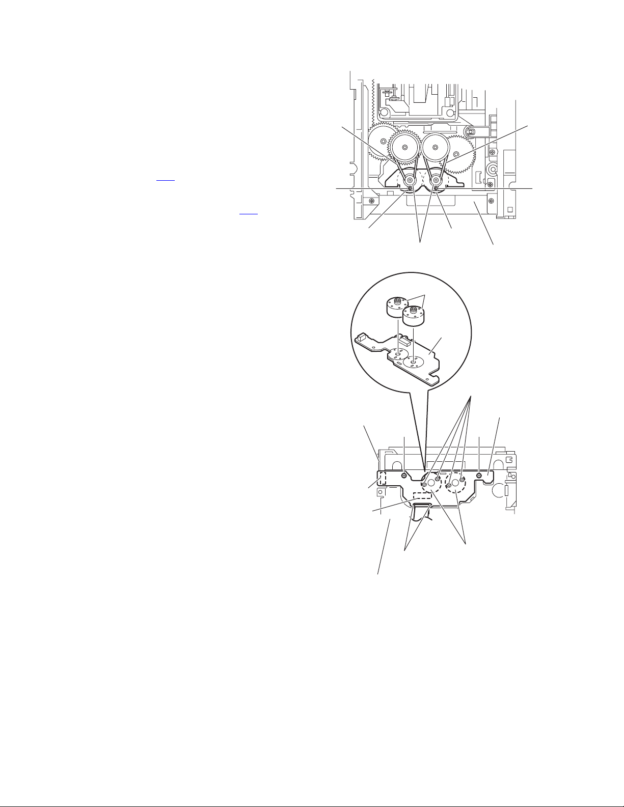
3.2.4 Removing the motor board
(See Figs.9 and 10)
(1) From the top side of the DVD changer mechanism assem-
bly, remove the two belts from the motor pulleys. (See
Fig.9.)
Note:
Take care not to attach grease on the belt.
(2) Remove the two screws D attaching the motors to the load-
er assembly. (See Fig.9.)
(3) From the bottom side of the DVD changer mechanism as-
sembly, remove the two screws E. (See Fig.10.)
(4) Disconnect the connector CN2
tray switch board and remove the motor board. (See
Fig.10.)
(5) Disconnect the card wire from the connector CN1
forward side of the motor board. (See Fig.10.)
Note:
When connecting the card wire, let the card wire through the
slots h of the motor board. (See Fig.10.)
Reference:
You need not to remove the tray assemblies, and in such case,
move it.
3.2.5 Removing the motor
(See Fig. 10)
• Remove the motor board.
(1) From the reverse side of the motor board, unsolder the four
soldered sections i on the motor board.
(2) From the forward side of the motor board, remove the mo-
tors.
on the motor board from the
on the
Belt
D
Motor Motor
Motor pulleys
Belt
D
Loader assembly
Fig.9
Motors
Motor board
i
Tray switch
board
E
CN2
CN1
h
DVD changer mechanism assembly
Fig.10
Motors
Motor board
E
1-20 (No.MB505)
Page 21

3.2.6 Removing the DVD traverse mechanism assembly
(See Fig.11)
• Remove the tray assemblies and DVD servo board.
(1) From the bottom side of the DVD changer mechanism as-
sembly, remove the three screws F attaching the DVD
traverse mechanism assembly.
(2) Remove the wires from the section j.
(3) Take out the DVD traverse mechanism assembly from the
DVD changer mechanism assembly.
DVD changer mechanism assembly
F
j
F
F
DVD traverse mechanism assembly
Fig.11
(No.MB505)1-21
Page 22

3.2.7 Removing the DVD pickup
(See Figs.12 to 14)
• Remove the tray assemblies, DVD servo board and DVD
traverse mechanism assembly.
(1) From the top side of the DVD traverse mechanism assem-
bly, release the lock of the connector on the DVD pickup
and disconnect the card wire in the direction of the arrow.
(See Fig.12.)
(2) Turn the screw shaft gear in the direction of the arrow 1 to
move the DVD pickup in the direction of the arrow 2. (See
Fig.12.)
(3) Remove the screw G attaching the feed bracket and re-
move the feed bracket from the sections k. (See Fig.12.)
(4) Release the claw m of the thrust spring in the direction of
the arrow and remove the thrust spring. (See Fig.12.)
(5) Remove the guide shaft from the sections (n, p) on the
C.TM chassis. (See Fig.13.)
(6) Remove the section q of the DVD pickup. (See Fig.13.)
(7) Remove the two screws H attaching the rack arm spring
and rack arm. (See Fig.14.)
(8) Pull the guide shaft from the DVD pickup in the direction of
the arrow. (See Fig.14.)
3.2.8 Attaching the DVD pickup
(See Figs.12 to 14)
(1) Attach the guide shaft to the DVD pickup and attach the
rack arm spring and rack arm with the screws H. (See
Fig.14.)
(2) Attach the section q of the DVD pickup to the C.TM chassis
first and attach the guide shaft to the sections (n, p). (See
Fig.13.)
Reference:
When attaching the guide shaft to the section p, attach it
under the rod spring. (See Fig.13.)
(3) Attach the thrust spring and feed bracket with the screw G.
(See Fig.12.)
(4) Turn the screw shaft gear in the direction of the arrow 1 to
move the DVD pickup in the direction of the arrow 2. (See
Fig.15.)
(5) Connect the card wire to the connector on the DVD pickup.
(See Fig.15.)
DVD traverse mechanism assembly
Thrust spring
Connector
Screw shaft gear
DVD pickup
Fig.12
DVD pickup
1
k
Thrust spring
q
Feed bracket
2
G
m
1-22 (No.MB505)
p
Rod spring
n
Guide shaft
C.TM chassis
Fig.13
Page 23

Guide shaft
DVD pickup
Rack arm
H
Rack arm spring
Fig.14
Connector
DVD pickup
222
Screw shaft gear
Fig.15
1
(No.MB505)1-23
Page 24

3.2.9 Removing the spindle motor board
(See Figs.16 and 17)
• Remove the tray assemblies, DVD servo board and DVD
traverse mechanism assembly.
(1) From the top side of the DVD traverse mechanism assem-
bly, remove the wires from the soldered sections r on the
spindle motor board. (See Fig.16.)
(2) From the bottom side of the DVD traverse mechanism as-
sembly, remove the three screws J attaching the spindle
motor board. (See Fig.17.)
Reference:
When attaching the spindle motor board, let the card wire
through the hole s on the C.TM chassis. (See Fig.17.)
DVD traverse mechanism assembly
Spindle motor board
r
Fig.16
DVD traverse mechanism assembly
s
J
C.TM chassis
Fig.17
1-24 (No.MB505)
Page 25

3.2.10 Removing the feed motor
(See Figs.18 and 19)
• Remove the tray assemblies and DVD traverse mechanism
assembly.
(1) From the top side of the DVD traverse mechanism assem-
bly, remove the screw K attaching the feed bracket and remove the feed bracket from the sections t. (See Fig.18.)
(2) Release the claw u of the thrust spring in the direction of
the arrow and remove the thrust spring. (See Fig.18.)
(3) Remove the screw shaft from the section v and remove it
in the direction of the arrow. (See Fig.19.)
(4) Remove the middle gear. (See Fig.19.)
(5) Remove the screw L attaching the feed motor to the C.TM
chassis. (See Fig.19.)
(6) Remove the wires from the soldered sections w on the
spindle motor board. (See Fig.19.)
(7) Take out the feed motor from the motor base.
Reference:
After attaching the feed motor, pass the wires through the sections x on the C.TM chassis as before. (See Fig.19.)
Feed bracket
Thrust spring
K
t
Thrust spring
Spindle motor board
w
x
Fig.18
Middle gear
v
Screw shaft
u
C.TM chassis
Fig.19
L
(No.MB505)1-25
Page 26

3.2.11 Removing the side (L) and tray switch board
(See Figs.20 to 22)
• Remove the tray assemblies.
(1) From the topside of the DVD changer mechanism assem-
bly, remove the two screws M attaching the side (L). (See
Fig.20.)
(2) From the left side of the DVD changer mechanism assem-
bly, disconnect the connector CN3
from the motor board and detach the side (L) in an upward
direction. (See Fig.21.)
(3) Remove the screw N attaching the tray switch board to the
side (L). (See Fig.22.)
(4) Release the joint tab y of the side (L) in the direction of the
arrow 1 and release the joint tab z while removing the tray
switch board in the direction of the arrow 2. (See Fig.22.)
on the tray switch board
SIde(L)
M
M
DVD changer mechanism assembly
Fig.20
M
Side(L)
M
CN3
Tray switch board
Motor board
Side(L)
Fig.21
y
1
1-26 (No.MB505)
2
z
Tray switch board
N
Fig.22
Page 27

3.2.12 Removing the side (R) assembly
(See Fig.23 to 27)
• Remove the tray assemblies and DVD servo board.
(1) From the inside of the side (R) assembly, release the two
tabs aa of the gear cover and remove the gear cover outward. (See Figs.23 and 24.)
(2) From the right side of the DVD changer mechanism as-
sembly, remove the elevator spring attached to the hook
ab of the loader assembly. (See Figs.24 and 25.)
(3) From the top side of the DVD changer mechanism assem-
bly, turn the gear 1 clockwise to move the elevator cam
rearward. (See Fig.25.)
(4) Move the two slots ac and joint ad of the elevator cam and
remove the elevator cam outward. (See Fig.25.)
(5) Remove the three screws P and detaches the side (R) as-
sembly upward. (See Figs.26 and 27.)
Note:
When reattaching the side (R) assembly, make sure to fit the
shaft (part ae) into the slot of the select lever. (See Fig.26.)
Side(R) assembly
aa
P
Elevator spring
ac
Fig.25
P
ae
ab
Elevator cam
acad
Select lever
Side(R) assembly
Gear cover
Loader assembly
P
Fig.23
Elevator spring
Gear 1
Side(R) assembly
Fig.26
P
ab
P
Fig.24
Side(R) assembly
Fig.27
(No.MB505)1-27
Page 28

3.2.13 Removing the lifter assembly
(See Figs.28 to 32)
• Remove the tray assemblies, DVD servo board, side (L) and
side (R) assembly.
(1) (1) From the top side of the DVD changer mechanism as-
sembly, turn the gear 1 clockwise to move the lifter assembly upward. (See Figs.28 and 29.)
(2) Turn the gear 2 clockwise to move the hook toward the
front until it stops. (See Figs.28 and 29.)
(3) Move the hook stopper in the direction of the arrow 2 while
pushing the tab af of the hook stopper to unlock it in the direction of the arrow 1 and release four joints ag to detach
from the rack holder. (See Fig.30.)
(4) Release the rod (L) from part ah. (See Fig.30.)
(5) Turn the gear 1 clockwise again to move the lifter assembly
upward. (See Fig.31.)
(6) Remove the lifter assembly from the DVD changer mecha-
nism assembly upward at the positions ai where the four
pins on the both sides of the lifter assembly fit to the notch-
es of the loader assembly. (See Fig.31.)
(7) Move the lifter assembly in the direction of the arrow and
release it from the hook. (See Fig.32.)
Hook stopper
Gear 2
Gear 1
ag
Rack holder
af
Hook
ag
1
ag
Hook stopper
Fig.30
Lifter assembly
ag
2
Rod(L)
ai
ah
ai
Hook
Gear 2
Lifter assembly
Fig.28
Gear 1
Lifter assembly
Gear 1
ai
Loader assembly
Fig.31
Lifter assembly
ai
Hook stopper
1-28 (No.MB505)
Hook
Fig.32
Hook
Fig.29
Page 29

3.2.14 Removing the sensor board and SV resistor
(See Fig.33)
• Remove the tray assemblies, side (L), side (R) assembly and
lifter assembly.
(1) Remove the solders from the soldered sections aj on the
sensor board and remove the wires.
(2) Remove the two screws Q and take out the sensor board
with the SV resistor.
Reference:
• Remove the soldered section ap on the sensor board as required.
• When reassembling, pass the wires through the slot ak of
the sensor board as before.
Note:
When reattaching the SV. resister, fit the projection am on the
bottom of the SV. resister into slot an of the sensor slider.
Sensor board
Q
ap
Q
ak
aj
SV resistor
am
an
SV resistor
Slider
Fig.33
(No.MB505)1-29
Page 30

3.2.15 Taking out the disc in the play mode
(See Fig.34 to 37)
Reference:
Refer to "3.3.1 Removing the tray assemblies".
(1) From the top side of the DVD changer mechanism assem-
bly, remove the top cover.
(2) Unlock the tray assemblies and draw out the tray assem-
blies toward the front.
(3) From the top side of the DVD changer mechanism assem-
bly, turn the gear 1 clockwise to move the lifter assembly
upward. (See Fig.34.)
(4) Turn the gear 2 clockwise to move the sub tray remaining
inside the lifter assembly toward the front, then pull out.
(See Fig.34.)
(5) Take out the disc on the sub tray. (See Fig.35.)
(6) After clearing away the disc, insert the sub tray into the
main tray. (See Fig.36.)
Note:
When reattaching the sub tray, move the tray stopper on
the bottom of the main tray in the direction of the arrow
to lock the sub tray certainly. (See Figs.36 and 37.)
(7) Push the tray assembly toward the DVD changer mecha-
nism assembly and reattach.
Tray assembly
Gear 2
Gear 1
Sub tray
Fig.34
Tray assembly
Fig.35
Disc
Sub tray
1-30 (No.MB505)
Page 31

Tray stopper
r
Main tray
Sub tray
Fig.36
Tray stoppe
Fig.37
(No.MB505)1-31
Page 32

SECTION 4
ADJUSTMENT
4.1 ATTENTION IN SERVICE OF DVD SECTION
(1) When pickup, Flash ROM ,DVD module board were changed, initialize EEPROM by all means.
(2) When full initialization was excuted, excute learning with a DVD test disc by all means.
Test disc : VT-501, VT-502
Learning method : It is adjusted automatically by normal playback of a DVD disc.
4.2 Test mode
Item Operation Managemant
Tray lock STOP [key] + DISC 1 EJECT
(Only during Stanby Mode)
Cold start [Remocon key]
STANDBY/ON + ENTER + 10
CLOCK
FAST FORWARDING
FAN ON/OFF Setting STOP [key] + DISC 2 EJECT
VOLUME LARGE
STEP CHANGE
MICON VERSION
DISPLAY
FL ALL SEGMENT
and TEMPERATURE
DATA
DVD test mode STOP [key] + EJECT 5[key]
[Remocon key]
STANDBY/ON + ENTER + 2
(During STANDBY MODE)
[Remocon Key]
STANDBY/ON + ENTER + 1
[Remocon Key]
STANDBY/ON + ENTER + 9
[Remocon Key]
STANDBY/ON + ENTER + >=10
(Hold during AC In)
Loader-Mehca is locked.
EJECT processing isn't done by pushing EJECT key at tray
lock state.
Then display to LOCKED/UNLOCKED.
EJECT 1 is pushed, pushing STOP again, tray lock is off.
Back up to tray locked ON/OFF.
Cold start processing.
After cold start is activated, FL temporary display
COLD' for 2 seconds. Then return to previous display.
To activate cold start AC OFF system, then AC ON again.
Fast Forward Clock (Increase clock counter speed)
Can only be activated after SYSTEM Clock is set
To exit this TEST mode, AC OFF the system, then AC ON
again.
Toggle between FAN switch ON and OFF.
( FANCTRL : L -> H TOGGLE )
This test mode is only effective during STANDBY MODE.
Need to set POUTREG to H when FANCTRL is H.
Test mode exit when system STANDBY -> P.ON
VOLUME CHANGE
VOLUME STEP MAX(40)
-> VOLUME STEP CENTER(20) TOGGLE
Normal Operation TEST mode.
System returns to normal operation after performing VOLUME
CHANGE.
TEMPORARY DISPLAY FOR MICON VERSION (5SEC)
After 5 seconds, return to previous display.
Each key press will toggle temporary display for the following:
SYSCON VERSION -> DVD LSI (BE) VERSION) and DVD
MECHA VERSION
* DVD LSI (BE & FE) VERSION CAN ONLY BEEN DISPLAY
DURING
SYSTEM POWER ON IN DVD MODE (WHEN DVD LSI P.ON)
* IF THERE IS NO INFORMATION FEEDBACK, SYS-CON
WILL DISPLAY
"WAIT" BLINKING 0.5SEC ON & OFF
Actual FL display SYSCOM version "012417-R**" or
"030227-R**"
FL ALL SEGMENT ON (NO BLINK)
Each key press will toggle between FL ALL SEGMENT, TEMP
decimal data and DVD THERMISTOR Temperature data.
Enters DVD-TEST mode.
DVD-TEST mode specification based on DVD-MODULE spec.
To exit DVD-TEST mode, AC OFF the system, then AC ON
again.
For Region Rewrite and DVD-AUDIO Device Key Writing,
refer to Region Rewrite and Device Key Writing section below
for exit procedure.
1-32 (No.MB505)
Page 33

Item Operation Managemant
DVD initialize >>| [key] during DVD test mode DVD module initialized.
FL 8 Segments will display 'INIT' after initialize.
" T xxy v0 " <- " T xxy vw "
Display will return to DVD Test Mode Area display.
( " T xxy vw " )
Press Power key to exit this TEST mode.
To exit this TEST mode, AC OFF the system, then AC ON
again.
DVD region confirm
mode
STOP [key] + EJECT 5[key]
(Hold during AC In)
FL display " T E*0 " (E=Euro) Region*
FL display " T E2 0 " (E=Euro) Region 2
or " TJC10 " (JC=USA/CANADA)Region 1
Tuner test mode [Remocon key]
Standby + enter + 0
eg: V U2 9K " VE 9K " Euro or " VJC 10K " (USA/CANADA)
V: version
U2: A/UF/UN/US
9K: AM STEP SETTING
SAFETY MODE check
by WHAT
STOP + LINE [key]
In standby [after safety trigger]
(A) If safety-cassette deck trigger, FL show : " ACM SAFETY "
(B) If /protect trigger, FL show : "AMP SAFETY"
(C) If /safety-reg trigger, FL show : "REG SAFETY"
(D) If flock trigger, FL show : "FAN SAFETY"
(E) If DVD temperature trigger, FL show : "DVD-SAFETY"
POWER KEY PRESSED to exit
*Note:
1. Other than Device Key Writing & DVD Region Re-write case, other test mode can be exit
by pressing POWER KEY on SET.
2. During any other Test Mode, when POWER KEY is pressed, wait until "POFF OK" displayed
(with Backlight LED off) meaning that DVD Test mode is successfully exit.
3. "POFF OK" Display will be indicated for 5sec only, then it will return to Standby Mode Display
4. After "POFF OK" dsiplay, system is now go back to normal operation mode.
4.3 Other test mode's operation
1. To enter DVD TEST mode,
a. AC POWER OFF
b. Press and hold STOP+DVD5 EJECT/CLOSE keys.
c. AC POWER ON while holding STOP+DVD5 EJECT/CLOSE keys.
d. Sys-con will send the following commands:
(INIT Command, TEST MODE Start)
(MODE STATE REPORT Command, DELIVERY INFO)
(STATUS REQUEST, DESTINATION AND REGION INFO)
(DESTINATION INFO, DESTINATION NUMBER, REGION INFO).
e. DVD Mecha will start in TEST MODE, FL will display:
Txxyvw
xx is the received DESTINATION information. Display as follows:
xx = JC/1U/D/E/2U/3U/UB/UT/4U/UY/EE/UF
y = region number
v = study state information from MECHA-CON (Display Byte3 when Byte7 is "0x09")
w = initialization state from MECHA-CON (Display Byte4 when Byte7 is "0x09".Display blank when Byte4 is "0xFF". )
2. To extie DVD TEST mode,
a. During TEST MODE (except for Device Key write & DVD Region Re-write), press POWER KEY
and wait until "POFF OK" is displayed for 5sec, then system goes into Standby Mode & Backlight LED is off
This means that System now successfully exit the DVD Test Mode & back to normal mode
b. To exit TEST mode for Device Key Write & DVD Region Re-write, first AC OFF,
then AC ON again to return to normal state.
(No.MB505)1-33
Page 34

3. EEPROM INITIALIZATION
(1) NORMAL INITIALIZE
a. During DVD TEST MODE, Press >>| key on remote control to start NORMAL EEPROM INITIALIZATION.
b. Sys-con will send the following command:
c. Mecha will feedback the following information after finish INITIALIZATION:
Status: Byte 0 = 0x00 (NORMAL), Byte 7 = 0x09, Byte 4 = initialization state
d. When received status, FL will display:
Txxyvw
w = initialization state from MECHA-CON (Display Byte4 when Byte7 is "0x09".Display blank when Byte4 is "0xFF". )
(2) FULL INITIALIZE
a. During DVD TEST MODE, STOP key on set 2 seconds control to start FULL EEPROM INITIALIZATION.
b. Sys-con will send the following command:
c. Mecha will feedback the following information after finish INITIALIZATION:
Status: Byte 0 = 0x00 (NORMAL), Byte 7 = 0x09, Byte 4 = initialization state
d. When received status, FL will display:
Txxyvw
w = initialization state from MECHA-CON (Display Byte4 when Byte7 is "0x09".Display blank when Byte4 is "0xFF". )
4. DEVICE KEY CHECKSUM DISPLAY
a. During DESTINATION INFO display screen (1), press MENU key to enter DEVICE KEY CHECKSUM display
(TEST MODE, MODE STATE, CHECK MODE)
(DEVICE KEY CHECKSUM)
FL will display (Example):
XXXXXX X DISPLAY BOTH CPPM AND CPRMX
5. DVD CHECK MODES
a. Press MENU key again to enter CHECK MODE.
(TEST MODE, MODE STATE, CHECK MODE)
FL Display:
HCEKC
Press '1' key on REMOTE CONTROL to START PLAYBACK.
FL Display:
ALPYABKC
Press '2' key on REMOTE CONTROL to perform SEARCH TNO+1
FL Display:
BOW B E (2 seconds)L
Status: 00(NORMAL) XX XX cc cc jj jj
ccccjj j cccc: Byte 0 = 0x00, Byte 7 = 0x00, Byte 3,4 ¨DISPLAY
Press '3' key on REMOTE CONTROL to perform SEARCH TNO-1
FL Display:
HCEKC
j
jjjj: Byte 0 = 0x00, Byte 7 = 0x00, Byte 5,6 ¨DISPLAY
FL Display:
1-34 (No.MB505)
Press '4' key on REMOTE CONTROL to light up CD_LD and display laser current.
LDC D R (2 seconds)
Status: 00(NORMAL) XX XX cc cc jj jj
ccccjj j cccc: Byte 0 = 0x00, Byte 7 = 0x00, Byte 3,4 ¨DISPLAY
Press '5' key on REMOTE CONTROL to light up DVD_LD and display laser current.
LS
j
(Static)
jjjj: Byte 0 = 0x00, Byte 7 = 0x00, Byte 5,6 ¨DISPLAY
Page 35

FL Display:
Status: 00(NORMAL) XX XX cc cc jj jj
Press '6' key on REMOTE CONTROL to enter DVD x 2 JITTER MEASUREMENT MODE
FL Display:
Status: 00(NORMAL) XX XX cc cc jj jj
Press '7' key on REMOTE CONTROL to view EEPROM (MECHA) content in -1 address step.
FL Display:
Status: 00(NORMAL) XX XX cc cc jj jj
Press '8' key on REMOTE CONTROL to view EEPROM (MECHA) content in +1 address step.
FL Display:
Status: 00(NORMAL) XX XX cc cc jj jj
LDC D R (2 seconds)
ccccjj j cccc: Byte 0 = 0x00, Byte 7 = 0x00, Byte 3,4 ¨DISPLAY
LS
j
(Static)
jjjj: Byte 0 = 0x00, Byte 7 = 0x00, Byte 5,6 ¨DISPLAY
TIJ X (2 seconds)
1
ccccjjjj
(Static)
cccc: Byte 0 = 0x00, Byte 7 = 0x00, Byte 3,4 ¨DISPLAY
jjjj: Byte 0 = 0x00, Byte 7 = 0x00, Byte 5,6 ¨DISPLAY
PEE B D (2 seconds)
ccccjjjj
W
(Static)
cccc: Byte 0 = 0x00, Byte 7 = 0x00, Byte 3,4 ¨DISPLAY
jjjj: Byte 0 = 0x00, Byte 7 = 0x00, Byte 5,6 ¨DISPLAY
PEE F D (2 seconds)
ccccjjjj
W
(Static)
Byte 3,4 ¨DISPLAY
jjjj: Byte 0 = 0x00, Byte 7 = 0x00, Byte 5,6 ¨DISPLAY
Press '9' key on REMOTE CONTROL to perform SEARCH DVD_SL DESIGNATED POSITION and
JITTER MEASUREMENT
FL Display:
Status: 00(NORMAL) XX XX cc cc jj jj
Press '10' key on REMOTE CONTROL to perform SEARCH DVD_DL PARALLEL DISC DESIGNATED
POSITION and JITTER MEASUREMENT
FL Display:
Status: 00(NORMAL) XX XX cc cc jj jj
Press '0' key on REMOTE CONTROL to perform monitor output.
FL Display:
Status: 00(NORMAL) XX XX cc cc jj jj
MPET (2 seconds)
ccccjjjj
(Static)
D-DLVD (2 seconds)
ccccjjjj
(Static)
NIT ROOM (2 seconds)
ccccjjjj
(Static)
cccc: Byte 0 = 0x00, Byte 7 = 0x00, Byte 3,4 ¨DISPLAY
jjjj: Byte 0 = 0x00, Byte 7 = 0x00, Byte 5,6 ¨DISPLAY
cccc: Byte 0 = 0x00, Byte 7 = 0x00, Byte 3,4 ¨DISPLAY
jjjj: Byte 0 = 0x00, Byte 7 = 0x00, Byte 5,6 ¨DISPLAY
cccc: Byte 0 = 0x00, Byte 7 = 0x00, Byte 3,4 ¨DISPLAY
jjjj: Byte 0 = 0x00, Byte 7 = 0x00, Byte 5,6 ¨DISPLAY
Press '>=10' key to INITIALIZE EEPROM (MECHA)
FL Display:
ITNI (2 seconds)
Press PLAY key on REMOTE CONTROL to start PLAYING and obtain LASER CURRENT and JITTER value.
(No.MB505)1-35
Page 36

FL Display:
RJ TISL (2 seconds)
Status: 00(NORMAL) XX XX cc cc jj jj
ccccjjjj
(Static)
cccc: Byte 0 = 0x00, Byte 7 = 0x00, Byte 3,4 ¨DISPLAY
jjjj: Byte 0 = 0x00, Byte 7 = 0x00, Byte 5,6 ¨DISPLAY
Press STOP key on REMOTE CONTROL to stop JITTER measurement.
FL display remains.
FFFF FFFF
(Static)
b. During CHECK mode, at any time press MENU key to exit CHECK mode and return to starting screen of DVD
TEST MODE.
* During TEST mode,at press POWER key send POWER OFF command to MECHA-CON and if poweroff permit
flag is 1, display "POFF OK"
FF KOOP
1-36 (No.MB505)
Page 37

SECTION 5
TROUBLESHOOTING
This service manual does not describe TROUBLESHOOTING.
(No.MB505)1-37
Page 38

Victor Company of Japan, Limited
Audio/Video Systems Category 10-1,1chome,Ohwatari-machi,Maebashi-city,371-8543,Japan
(No.MB505)
Printed in Japan
VPT
Page 39

SCHEMATIC DIAGRAMS
MICRO COMPONENT SYSTEM
UX-G70J,UX-G70C,UX-G70B,UX-G70E
UX-G70EN,UX-G70EV,UX-G70EE
CD-ROM No.SML200606
SUPER VIDEO
Lead free solder used in the board (material : Sn-Ag-Cu, melting point : 219 Centigrade)
Contents
Block diagrams
Standard schematic diagrams
Printed circuit boards
COPYRIGHT 2006 Victor Company of Japan, Limited.
CA-UXG70
SP-UXG70SP-UXG70
2-1
2-3
2-19 to 24
No.MB505SCH
2006/6
Page 40

In regard with component parts appearing on the silk-screen printed side (parts side) of the PWB diagrams, the
parts that are printed over with black such as the resistor ( ), diode ( ) and ICP ( ) or identified by the " "
mark nearby are critical for safety.
Page 41

< MEMO >
Page 42

Block diagram
A
R
DVD section
A, B, C, D, RF+/-, LPC1, LPC2
CN101
DVD pickup
mechanism
DVD traverse
mechanism
E1+F1, E2+F2, E3+F3, E4+F4
LD(CD)
FM+/WOUT
VOUT
UOUT
CN201
COM
LD(DVD)
F+/T+/-
IC201
DRVER
DVD changer mechanism section
SW1 to SW5
TRAY1 to 5
CLOSE SW
M1,M2
TRAY/POSITION
MOTOR
Q101 to Q104
LASER
DRIVER
SPDRV, TRSDRV
FODRV, TRDRV
/SPMUTE, /DRVMUTE, FG
IC510
SDA,SCL,WP
EEPROM
TR1_CL to TR5_CL
M.TR_OP
CN3
CN2
M
IC1, IC2
TRAY / POSITION
MOTOR DRIVER
LPCO1
LPCO2
CDLDCUR
DVDLDCUR
X301
27MHz
SW6
TRAY
OPEN SW
IC301
DV3.2
TRVSW
R1
POSITION
SENSOR
SW8
SUB TRAY
END SW
POS_UP, POS_DOWN
TR_OP, TR_CL
MA0 to 11, MDQ0 to 15
BA0, BA1, MCK, DQM0, DQM1
NCSM, NRAS, NCAS, NWE
LRMUTE
BCK, LRCK, DACCK, AOUT0
DAC0CS, DCLK, DDATA, DACPDN
IC505
SDRAM
IC701
AUDIO ADC
TX, DAC1OUT, DAC2OUT, DAC3OUT, DAC4OUT, DAC5OUT
EXDT0 to 15,
EXADT0 to 15
EXADR16 to 20
NEXCE, NEXOE
NEXWE
S2UDT, U2SDT, UCS
UCLK, SCS, CPURST
DISCSET, DISCSTP
CPURST
RESET
CN453
W2
LSENSOR
IC509
FLASH
ROM
IC453
IC451
IC302
D1.2V
REG.
IC305
3.3V
REG.
DVDPWR
DISPRST
DISPBUSY
DISPCS
DISPCK
DISPD2S
DISPS2D
MECHA
W1
CN1
CN452
STEDSW
CLSWT1 to 5
MTOPSW
POSMUP
CN451
POSMDN
MTOP, MTCL
CONTROLLER
X451
8MHz
EEPROM
FAOUTL
FAOUTR
IC705
A5V
REG.
EPDI
EPDO
EPCS
EPSK
IC452
CN702
CN503 CN504
CN701
CN501 CN502
2-1
AC
INPUT
CN906
T9000
TRANSFORMER
RY901
POUT
RELAY
D9001 to D9004
DIODE BRIDGE
Transformer section
D9044 to D9047
DIODE BRIDGE
+VH, -VH
S1
+VL, -VL
D9011 to D9014
DIODE BRIDGE
S2
IC901
US6V
REG.
SUB6V
S12V
S3
D9021 to D9024
DIODE BRIDGE
S3
S1
S3CT
CN901
CN903 CN904
T9001
TRANSFORMER
T
F
S4
TUNE
UNIT
Page 43

Audio amplifier & Regulator section
CN301
CN356 CN351
E.VOLUME
/SMUTE
CN703
/PRT
AMPCTRL
FAOUTL
FAOUTR
LRMUTE
CN704
3.3V to 5.5V
CONVERTER
EEPROM
Q7301
RESET
AMPCTRL
Q3051 to Q3054
IC STANDBY
CTRL
R_OUT, B_OUT, Y/G_OUT, Y_OUT, C_OUT
SPDIF(TX)
Q3541
FLVH
S1
30V REG.
S4
CN361
CN358
CN701
AHB
FB
/AHB
INL/R
GAMEL/R
SWL/R
Q2250
Q2260
IC200
&
HPF
VOLCLK
VOLDATA
VOLCE
DVDL/R
Q2600,Q2601
Q2610
LRMUTE
DISPRST, DISPCS
DISPCK, DISPD2S
DISPBUSY
DISPS2D
/RESET
DISPBUSY
DISPS2D
EEP-SCL
EEP-SDA
IC703
IC702
IC301
POWER AMP.
IC300
USB3.3V REG.
POUT
CN702
SPKRLY
FAN-LDT
POUT
/SAFETY
/SMUTE
IC701
SYSTEM
MICON
/PRT
/SMUTE
+VH, -VH, +VL, -VL
USB3.3V
GAMEL/R
CN360CN357
Used for
Area suffix J/C
SPDIF(TX)
Q2300
to Q2302
SW MUTE
LOUTSE-DET
HPSW
AUXSW
QPL
/LOMUTE
IC250
J230
/SWMUTE
V-MUTE, VIDEORGB,
VIDEOYC, VIDEO-SW
VS1, VS3, BLANK-CTL
Q3011,Q3111
Q3061 to Q3064
PROTECTOR
Q3041 to Q3043
SYSTEM MUTE
CN359
OPTICAL
DIGITAL
OUT
SUBWOOFER
OUT
CN705
SCART-LIN
SCART-RIN
Q7900
Q7901
Q7999
LINE OUT
DET.
USBL/R
AUXL/R
HPL/R
LSEL0
RSEL0
LOUTL
LOUTR
OUTL
OUTR
CN302
CN353
+VH
-VH
+VL
-VL
INL
INR
Q3551 to Q3555
H/P MUTE
/SMUTE
CTRL
/SAFETY_REG
D3210
to D3512
D3514
D3516
INL
INR
SAFETY
DET.
S3, S3CT
CN355
Video section
Used for Area suffix B/E/EN/EV/EE
Q4006
Q4007
VIDEO
CN401 CN402
VIDEORGB
VIDEOYC
SW
COUT, YOUT
B-Y/B_OUT
Y/G_OUT
R-Y/R_OUT
V-MUTE
VIDEORGB
VIDEO-SW
Q4201 to Q4204
SCREEN MODE
VS1, VS3, BLANK-CTL
Used for Area suffix J/C
Front panel section
FW120
CN713
GAMEL/R
FW121
USB3.3V
FW130
GAME IN AMP.
Used for Area suffix J/C
AUXLIN, AUXRIN
QPL
AUXSW
IC140,IC141,Q1450
LINE IN AMP. & QP-LINK
LOUTL/R
/LOMUTE
X1300
12MHz
OUTL
OUTR
Q3561,RY351
SPK RELAY
SPKRLY
CN354
CN801
CTRL
IC831
DVD5V
DVD5V
SCART-LIN, SCART-RIN
IC401
VIDEO
DRIVER
FUNCTION
BLANKING
Py/G OUT
Pb/B OUT
Pr/R OUT
CV OUT
IC402
VIDEO SW
GAMEPOS
CN405
FW110
IC150
GAMEPOS
Q1410 to Q1412
LINE OUT MUTE
IC130
USBL/R
D/A
J3501
Q8001 to Q8003
VOLTAGE CTRL
S3CT
IC821
S9V
REG.
REG.
S9V
CN403
J4001
C OUT
J4002
Y OUT
C/R
GAME
VIDEO
/AUDIO
INPUT
HPL/R
J1200J1500 J1300
HPSW
HEADPHONE
OUTPUT
J1400
J1410
D+/HOST
USB AUDIO
INPUT
TO
SPEAKER
S3
IC811
S12V
REG.
S12V
SCART
TERMINAL
COMPONENT
VIDEO OUT
COMPOSITE
/S-VIDEO
OUT
LINE
INPUTPUT
LINE
OUTPUT
T
TO
FAN
ER
X7001
8MHz
FLOCK
CN708 CN712
Q7400,Q7401
FON1
FAN DRIVER
RDSON, RDSCLK
RDSDATA
TUCE, TU-DIN
TU-DOUT, TUCLK
TUL/R
System Control & Audio section
FLVH
FL-CTL
Q7807
Q7808
REM
STB-LED, BKLED
FL-CLK, FL-LATB
FL-DATA, FL-BK
FKEY1, FKEY2
VOLM, VOLP
FL1
FL2
FLVH
CN706
IC101
REMOCON
D1020, Q1020
BACK LIGHT
CN 111
S1100 to S1121
KEY MATRIX
REM
BKLED
FKEY1
FKEY2
FL1, FL2
FLVH
FL-BK
FL-CLK
FL-DATA
FL-LATB
CN100
CN110
D1105,Q1100
STANDBY LED
DI100
FL DISPLAY
SEG1 to SEG20
GRID1 to GRID13
IC100
FL DRIVER
STB-LED
VOLUME
VOLM
VOLP
JS110
2-2
Page 44

Standard schematic diagrams
Primary section
CN901
QGB2510J1-14
0V
AMPGND
1
0V
AMPGND
2
0V
INH
3
0.1V
S1
4
47.6V
+VH
5
-47.6V
-VH
6
22V
+VL
7
-22V
-VL
8
19.19V
S3
9
(PAGE 2/9)
0V
S3GND
10
8V
S3CT
11
5.6V
12
SUB6V
4.3V
13
POUT
TO CN351 OF GVA10129-A2
11.9V
S12V
14
B9100
1SS133-T2
0.1V
0.8V
0V
NI
Q9031
US6V
VIN
123
11.2V
D9048
GND
0.7V
D9025
2A02-M
R9033
R9032
IC901
KIA7805API
5.6V
GVA10129-A1
C9011
NI
MY
!
D9011
1N5402M-20
!
MY
D9012
C9012
1N5402M-20
1N5402M-20
0.1/100
C9013
INHB
C9031
NI
4.3V
Q9044
KRC111M-T
R9031
D9032
NI
NI
VOUT
C9041
100/16
!
MY
MY
D9014
C9015
0.1/100
1N5402M-20
D9013
!
NI
NI
C9014
MY
NI
D9031
NI
1N4003S-T5
0.1V0V
C9043
1000/25
0.1/100
!
D9040
1N4003S-T5
1N4003S-T5
1N4003S-T5
1N4003S-T5
D9044
D9045
D9046
D9047
MY
MY
C9002
0.1/250
C9022
C9001
NI
MY
D9001
1N5402M-20
!
MY
D9003
D9002
1N5402M-20
1N5402M-20
!
MY
NI
C9003
QMF51U1-3R15-J8
C9021
MY
NI
D9021
1N5402M-20
!
MY
D9023
1N5402M-20
D9022
1N5402M-20
0.1/100
!
MY
NIC9023
D9043
1SS133-T2
QSK0129-002
71
6
5
**
!
T9000
QQT0253-012
!
R9050
3.3M
QRZ9037-335
EP901
QNZ0136-001Z
!
D9004
C9005
1N5402M-20
0.1/250
F9003
!
D9024
C9025
0.1/100
1N5402M-20
12
!
RY901
4
!
MY
0.1/250
C9004
3.15A/125V
F9006
!
QMF51U1-2R5-J8
2.5A/125V
!
MY
0.1/100
C9024
C9044
QCZ9105-472
34
MY
**
!
LF901
F9001
!
QMF51U1-6R3-J8
6.3A/125V
F9002
!
QMF51U1-6R3-J8
6.3A/125V
QMF51U1-3R15-J8
3.15A/125V
!
F9004
B9304
4
NI
1
23
B9305
C9052
NI
!
!
NEUTRAL
CN906
QGA7901C1-02
F9008
21
14.6V
14.6V
33.0V
33.0V
6.2V
6.2V
120V
5A/125V
QMF51U1-5R0-J8
LIVE
!
CN903
QGA3901C1-08
0V
1
GND
S2
2
3
S2
S1
4
S1
5
0V
S3CT
6
S3
7
8
S3
CN904
QGA7901C1-03
3
2
0V
1
FROM TRANSFORMER
NI
C9051
FROM TRANSFORMER
TRANSFORMER (J/C)
GND
1
S2
2
S2
3
S1
4
S1
5
S3CT
6
S3
7
TO CN903 OF
GVA10129-A1
S3
8
3
120V
2
0V
1
GVA10129-A1
TO CN904 OF
!
120V
S1
S2
GND
S2
S1
S3
S3CT
S3
S4
0V
S4CT
0V
S4
T9001
**
QQT0510-001
TO CN361 OF GVA10129-A2
(PAGE 2/9)
S4CT
S4
123
S4
2-3
**
REF. NO.
T9001
T9000 QQT0253-002 QQT0253-002 QQT0370-012 QQT0253-012 QQT0253-013
LF901
B9304
B9305
B9200
B9201 NI
CN905 NI
F9006
F9007
F9008 QMF51W2-5R0-J8
NOTES
1.
VOLTAGES ARE DC-MEASURED WITH A DIGITAL
VOLT METER
CONDITION ---
UNLESS OTHERWISE SPECIFIED.
2.
ALL RESISTORS ARE CARBON FILM RESISTOR
ALL CAPACITORS ARE
MYLAR CAPACITOR.
ALL RESISTANCE VALUES ARE
ALL CAPACITANCE VALUES ARE IN F(P=pF).
ALL CAPACITORS ARE SHOWN IN THE FORM
OF
ALL INDUCTANCE VALUES ARE IN H(m=mH).
3.NI = NO INSERT
UP
QQT0510-004 QQT0510-003
NIS9001
QQR1321-001
NI
NI
INSERT
NI
QMF51W2-3R15-J8 QMF51W2-3R15-J8 QMF51W2-3R15-J8
NI
QMF51W2-2R5-J8
OR OSCILLOSCOPE WITHOUT INPUT SIGNAL.
DVD STOP MODE
1/4W
CAPACITANCE( F)
QMF51W2-2R5-J8
5%
CERAMIC CAPACITOR
IN OHM( ).
/RATED VOLTAGE (V).
QQT0510-004
NI
NI
INSERT
INSERT
NI
INSERT
NI
NI
A
US/UX/UN/UG/UJ
QSW0812-001
NI
INSERT
INSERT
INSERT
QGA7901C1-04
QMF51W2-2R5-J8
OR
J/C E/EN/B/EV/EE
QQT0510-001 QQT0510-002
NI NI
NI
INSERT
INSERT
INSERT
NI
NI NI
QMF51W2-2R5-J8 QMF51W2-3R15-J8
NI NI
QMF51u1-5R0-J8
QQR1321-001
INSERT
NI
QMF51W2-2R5-J8
NI
NI
Page 45

CN901
QGB2510J1-14
0V
AMPGND
1
0V
AMPGND
2
0.1V
INH
3
0V
S1
4
47.6V
+VH
5
-47.6V
-VH
6
23.4V
+VL
7
-23.4V
-VL
8
21.1V
S3
9
(PAGE 2/9)
0V
S3GND
10
8.7V
S3CT
11
5.6V
12
SUB6V
4.3V
13
POUT
TO CN351 OF GVA10129-A2
11.8V
S12V
14
GVA10129-A1
0.1/100
!
!
MY
D9001
1N5402M-20
MY
D9002
1N5402M-20
1N5402M-20
!
MY
D9021
1N5402M-20
MY
D9022
1N5402M-20
1N5402M-20
!
C9001
NI
!
C9005
0.1/250
D9003
MY
NIC9003
QMF51W2-3R15-J8
C9021
NI
!
C9025
0.1/100
D9023
MY
NIC9023
!
MY
D9004
1N5402M-20
F9003
QMF51W2-3R15-J8
!
MY
D9024
1N5402M-20
!
3.15A/250V
F9006
C9004
C9024
0.1/250
0.1/100
QMF51W2-6R3-J8
QMF51W2-6R3-J8
QMF51W2-3R15-J8
!
3.15A/250V
F9001
!
6.3A/250V
F9002
!
6.3A/250V
3.15A/250V
F9004
CN903
QGA3901C1-08
0V
1
GND
14.1V
2
!
S2
14.1V
S2
3
29.9V
S1
4
29.9V
S1
5
0V
S3CT
6
6.3V
7
S3
6.3V
8
S3
C9011
NI
MY
!
---
1N5402M-20
!
MY
C9012
1N5402M-20
D9012
1N5402M-20
0.1/100
D9025
2A02-M
R9032
R9033
INHB
NI
D9032
NI
NI
C9031
0.1V
0.8V
B9100
NI
0V
Q9031
MY
!
R9031
NI
D9013
!
MY
D9014
C9015
0.1/100
1N5402M-20
C9014
MY
NIC9013
NI
D9031
NI
0.1/100
MY
C9002
0.1/250
MY
C9022
TRANSFORMER (B/E/EN/EV/EE)
GND
1
S2
2
S2
3
S1
4
S1
5
S3CT
6
S3
7
GVA10129-A1
TO CN903 OF
S3
8
3
230V
2
0V
1
TO CN904 OF
GVA10129-A1
FROM TRANSFORMER
!
230V
0V
0V
**
T9001
QQT0510-002
TO CN361 OF GVA10129-A2
(PAGE 2/9)
S1
S2
GND
S2
S1
S3
S3CT
S3
S4
S4CT
S4
S4
123
S4CT
S4
US6V
123
11.2V
D9048
1SS133-T2
!
D9040
C9043
1000/25
1N4003S-T5
1N4003S-T5
1N4003S-T5
1N4003S-T5
1N4003S-T5
D9046
D9047
4.3V
D9044
D9045
0V
IC901
KIA7805API
GND
VIN
VOUT
5.6V
0.7V
C9041
100/16
0.2V
KRC111M-T
Q9044
D9043
1SS133-T2
!
QQT0253-013
T9000
12
!
RY901
QSK0129-002
**
C9044
QCZ9105-472
34
**
!
MY
LF901
EP901
B9304
NI
4
1
QQR1321-001
NI
B9305
C9052
NI
NI
23
NEUTRAL
CN906
QGA7901C1-02
!
F9008
21
230V
2.5A/250V
QMF51W2-2R5-J8
LIVE
!
3
2
0V
1
CN904
FROM TRANSFORMER
QGA7901C1-03
NI
C9051
Parts are safety assurance parts.
When replacing those parts make
sure to use the specified one.
2-4
Page 46

Amplifier section
KTA1268/GL/ T
4
4
0
6
V
O
/SMUTE
AMPCTRL
/PRT
US6V
US6V
(PAGE 3/9)
1
2
3
4
5
QGF1205C2-05
CN301
4.8V
3.7V
4.8V
4.8V
4.8V
C3001
D3051
C3053
100/16
C3063
10/50
46.8V
D3061
KTC3199/GL/-T
1SS133-T2
R3065
10K
R3056
G
2.2K
46.8V0V
Q3064
100K
R3066
!
*
POWER IC
IC301
+VH
+VL
+REF
-REF
-VL
-VH
GND
+RE/LCH
-RE/LCH
-RE/RCH
+RE/RCH
-PRE(-VH)
+PRE(+VH)
LIN
-LIN
CCBIAS
-RIN
RIN
181716151413121110987654321
0V
0V
0V
0V
1K
D3011
5.6K
D3111
1SS133-T2
1K
R3111
*2*2
C3115
0.022/50
R3112
1SS133-T2
5.6K
R3113
0V
R3120
1K
0V
0.22
46.8V 0V
R3114
47V
8.9V
23.2V
D3002
MTZJ15B-T2
NI
D3001
6.8K
6.8K
R3002
R3003
MTZJ36B-T2
C3012
47/25
UNF
R3019
1K
MY
-8.8V
MTZJ15B-T2
6.8K
R3004
C3011
4.7p
R3015
47K
C3013
0.33/50
UNF
R3016
2.2
UNF
R3017
MY
C3014
0.33/50
R3005
2.2
-23.1V
-47V
D3003
6.8K
MTZJ36B-T2
D3004
100K
R3018
C3002
L3011
0.39
!
NI
10
R3006 UNF
0.022/50
Q3011
46.9V
KTC3200/GL/-T
47K
R3014
0V
C3015
R3012
0.22
R3020
R3011
1K
0V
R3013
-46.2V
KTC3200/GL/-T
Q3111
47K
L3111
0V
0V
46.2V
C3016
47P
R3007
C3111
4.7p
R3115
47K
0.39
UNF
R3116
2.2
UNF
R3117
UNF
2.2
1K
R3119
MY
C3113
0.33/50
100K
R3118
MY
C3114
0.33/50
B3111
D3041 NI
-44.9V
C3112
47/25
33K
R3041
0V
C3116
R3131
47K
R3031
47K
C3041
220
0V
47P
Q3041
KRA109M-T
4.8V -1V
4.7/50
Q3042
KTC2876-T
20K
R3042
10/35
C3031
10/35
4.8V
C3131
0V 0V
KTC1027/OY/-T
C3132
C3032
100P
10K
R3043
0V
Q3043
KTC2876-T
SYSTEM MUTE
MY
100P
KTA1023/OY/-T
R3132
1.5K
MY
R3032
1.5K
10K
R3044
0V
0V0V
Q3052
-46.3V
R3034
Q3051
R3133
R3033
3.3K
46.3V
56K
56K
R3134
-45.7V
C3054
1/50
-46.3V
3.3K
IC STANDBY CTRL
R3052
45.8V
46.3V
R3054
10K
C3051
47/63
!
R3057
R3051
10K
10K
R3053
10K
47
R3058
UNF
KTC3200/GL/-T
0.7V
0.6V
KTA1268/GL/-T
C3052
47/63
47
!
UNF
10/50
C3061
R3061
-47.1V
100K
R3062
-46.5V 4.8V
0V 0V
0V
R3063
KTA1268/GL/-T
Q3062
Q3053
0.6V
Q3054
10K
100K
1.3V
R3055
0V
PROTECTOR
Q3061
KTC3200/GL/-T
-47.1V
4.8V
R3064
10K
0V
47/25
C3062
1SS133-T2
100K
Q3063
FROM CN703 OF GVA10128-A1
J3501
QNB0303-001
2
1
4
3
C3567
C3568
0.001/50
CN359
SGND
QGD2504C1-05Z
0V
HPR
5
0V
HPGND
4
0V
3
HPL
0V
DGND
2
3.3V
1
USB3.3V
3.7V
GAMEL
3
0V
AGND
2
3.7V
GAMER
1
(PAGE 4/9)
CN360
FROM FW120 OF GVA10128-A4
QGD2504C1-03Z
*1
NOTES
1. VOLTAGES ARE DC-MEASURED WITH A DIGITAL
VOLT METER
CONDITION --- DVD STOP MODE
2. UNLESS OTHERWISE SPECIFIED.
ALL RESISTORS ARE 1/4W 5% CARBON FILM RESISTOR.
ALL CAPACITORS ARE OR
MYLAR CAPACITOR.
ALL RESISTANCE VALUES ARE IN OHM( ).
ALL CAPACITANCE VALUES ARE IN F(P=pF).
ALL CAPACITORS ARE SHOWN IN THE FORM
CAPACITANCE( F) /RATED VOLTAGE (V).
OF
ALL INDUCTANCE VALUES ARE IN H(m=mH).
ALL DIODES ARE 1SS133-T2 UNLESS SPECIFIED
3.NI = NO INSERT
**
C3562
NI
R3565
R3566
0.001/50
REF. NO.
B3190
B3191 QUY0150-050YNI
B3192
R3200
OR OSCILLOSCOPE WITHOUT INPUT SIGNAL.
NI
NI
C3561
C3563
NI
C3565
NI
NI
NI
C3564
C3566
NI
PQ033ES3MX-T
IC300
123
3.3V 8.7V
D3212
47/25
C3212
MTZJ3.9B-T2
J/C ONLY
QUY0150-050Y NI
NI QUY0150-050Y
100
CERAMIC CAPACITOR
B3166
4
6
4
6
B3167
INGNDOUT
0V
NI
LF351
13
B3165
B3168
NI
LF352
13
*1
B3192
*1
R3200
C3210
47/25
OTHERS
NI
!
QSK0127-001
321
RY351
D3561
1SS133-T2
*2
REF. NO.
C3015
C3115
SPEAKER
RELAY
65 4
UNF
680
R3560
Q3555
KTC2876-T
0.5V
0V
-1.5V
4.7K
R3559
ALL VERSION
0.022/50
0.022/50
DIGITAL TRANSISTOR
CONSTRUCTION
R2
R1
R2
R1
R1R2KRC102M-T
KTC3199/GL/-T
Q3554
KTC2876-T
-1.4V
4.7K
R3558
KRA109M-T
KRA110M-T
Q3541
!
0V
9V
INR
A9V
AGND_IN
OTHERS
OTHERS
QUY0150-050Y
NI
NI
NI
2.4V
SPK_RLY
30V REG
R3546
1.6V
3.3V
123456789
3.3V
SPDIF
KTC2026/Y/
31.9V
32.4V
C3545
0.01/16
NI
D3545
C3546
22/50
MTZJ33B-T2
REF. NO. OTHERS
***
Q3301
R3504
R3503
B3179
REF. NO.
**** OTHERS
D8001
80V
33K
R3545
R3544
C3544
KRA110M-T
QRT01DJ-R33X
QRT01DJ-R33X
R3561
0.1V
1.5K
0.9V
Q3561
0.2V
0V
-0.8V
R3557
Q3553
KTC2876-T
0.3V
Q3552
-0.8V
4.7K
R3556
R1 R2
47K 22K
4.7K
10K 10K
UNFR3555
KTC2876-T
0V
4.7K
680
-
1SS133-T2
R3554
5.3V
-0.6V
KRA109M-T
D3551
220
Q3551
**
H/P MUTE
C3551
4.7/50
*
82K
1SS133-T2
R3553
47K
CN358
QGB2510K2-11
REF. NO.
IC301
REF. NO.
B3165
B3166
B3167
B3168
R3565
R3566
C3561
C3564
C3562
C3563
C3565
C3566
82K
R3563
R3562
82K
82K
D3552
D3553
1SS133-T2
R3551
R3552
0V
0V5V0V
0V
0V
11.8V
10
11
FB
INL
S12V
LEVEL
MGND
TO CN701 OF GVA10128-A1
(PAGE 3/9)
J/C
STK412-490-ESTK412-400
B/E/EN/EV/EE
UP
NI
4.7 OHM
3300P/50
47000P/50
D3544
1N4003S-T5
33K
D3543
1N4003S-T5
22/50
C3543
47/100
CN361
QGA2501C1-03
FROM TRANSFORMER
(PAGE 1/9)
J/C
NI
J/C
C3542
100/63
D3542
1N4003S-T5
NI
QUY150-050Y
MTZJ5.6C-T2MTZJ5.1C-T2
UNF
4.7
!
10/50
5.6V
S4CT
R354
NI
R35
0.6V
9.1
R35
D3541
MTZJ5.6B-T2
9.1
B31
NI
5.6V
123
S4
0V
C3541
5.6V
S4
T
R3543
2-5
Page 47

100K
G
C3543
3
.
C
/
Q3053
KTC3200/GL/-T
0.7V
1.3V
0.6V
0V
0.6V
Q3054
KTA1268/GL/-T
C3052
47/63
10K
R3061
Q3061
KTC3200/GL/-T
-47.1V
1V
4.8V
R3064
10K
5V 4.8V
0V 0V
100K
R3063
47/25
C3062
C3542
544
03S-T5
1N4003S-T5
D3543
1N4003S-T5
47/100
R3055
100K
PROTECTOR
0V
Q3063
100/63
D3542
D3051
1SS133-T2
100/16
KTC3199/GL/-T
R3543
UNF
4.7
!
0V
C3541
C3053
D3061
10/50
C3063
10/50
R3056
2.2K
R3065
10K
46.8V
1SS133-T2
0.6V
D3541
GVA10129-A3
46.8V0V
Q3064
KTA1268/GL/-T
100K
R3066
R3548
R3540
NI
NI
R3541
R3549
9.1
NI
R3542
R3550
MTZJ5.6B-T2
9.1
NI
B3161
B3160
NI
OUTL
OUTR
+VH
-VH
PGND
PGND
+VL
-VL
INL
AGND_IN
INR
CN302
QGB2510K1-11
1
2
46.8V
3
-46.8V
4
5
6
23.1V
7
-23.1V
8
9
10
11
0V
0V
0V
0V
0V
0V
0V
0V
0V
0V
0V
0V
0V
0V
GVA10129-A2
CN353
QGB2510J1-11
OUTL
1
OUTR
2
+VH
3
-VH
4
PGND
5
PGND
6
+VL
7
-VL
8
INL
9
AGND_IN
10
INR
11
SGND1
FROM CN901 OF GVA10129-A1
EP351
QNZ0136-001Z
AMPGND
0V
R3501
22K
C3506
3300/35
C3505
3300/35
4700/56
R3502
C3502
4700/56
C3503
4700/16
C3504
4700/35
C3501
22K
B3178
(PAGE 1/9)
+VL
AMPGND
+VH
-VH
INH
S1
123456789
0V
0V
0.1V
46.7V
22.9V
-46.7V
-22.9V
(1W)
R3504
0.33
19.3V
KRA110M-T
Q3301
0.4V
D3521
D3522
NI
NI
D3524
1N4003S-T5
D3525
NI
-VL
19.3V
100/16
100/16
21.1V
R3300
2A02-M
C3521
C3522
S3CT
S3
S3GND
1011121314
0V
8.9V
***
NI
B3179
0.33
R3503
(1W)
0.4V
4.7K
D3523
SUB6V
POUT
5.6V
4.3V
MTZJ13B-T2
MTZJ11C-T2
D3514
1SS133-T2
0V
KRC102M-T
4V
D3517
MTZJ5.6A-T2
1SS133-T2
S12V
CN351
QGB2510K2-14
11.8V
1SS133-T2
1SS133-T2
D3515
D3511
1SS133-T2
SAFETY
D3500
Q3300
D3516
SAFETY_REG
D3510
D3512
R3512
VOLTAGE CTRL
Q8001
!
KTA1046/Y/
21.1V
1k
8.6V
20.6V
0V
KTC3199/GL/-T
1k
R8002
0V
Q8002
R8003
R8005
4.7k
R8004
C8001
220P/50
680
R8006
0.7V
Q8003
1k
0V 0V
KTC3199/GL/-T
D8001
****
C8002
0.01/50
2.7k
680
R8007
R8001
IC811
!
KIA7812API
21.1V
123
R8201
IN
B8101
!
1234
!
1234
!
123
GND
OUT
IC821
KIA278R09PI
IN
OUT
GND
CTRL
IC831
KIA278R05PI
IN
OUT
GND
CTRL
IC841
NI
IN
GND
S12V
DVD5VS9V
M5V
0V
11.8V
D8101
NI
NI
UNF
21.1V
9.1V
0V
21.1V
B8100
8.6V
5V
0V
4.8V
B8300
OUT
C8101
10/50
C8102
D8201
100/25
C8201
10/50
NI
C8202
100/25
C8203
0.01/50
R8301
NI
UNF
C8301
10/50
C8302
100/16
C8303
NI
D8301
NI
C8401
NI
C8402
NI
CN354
QGB2510J1-09
S3
GND
S3CT
S12V
A9V
M9V
M5V
S5V
CTRL
NI
CN801
QGB2510K1-09
21V
S3
1
1
0V
GND
0V
2
2
8.9V
S3CT
3
3
S12V
11.8V
4
4
A9V
9.1V
5
5
M9V
9.1V
6
6
5V
M5V
5V
7
7
S5V
5V
5V
8
8
CTRL
4.8V
9
9
GVA10129-A4
CN355
QGF1205C2-10
R_OUT
3.1V
1
VGND
0V
2
B_OUT
3.1V
3
VGND
0V
4
Y/G_OUT
3.2V
5
VGND
0V
6
Y_OUT
3.2V
7
D5V
5V
8
C_OUT
3.1V
9
11.8V
12V
10
(PAGE 5/9)
TO CN401 OF GVA10129-A5
*1
B3191
C3500
4.7/50
CN361
5.6V
A2501C1-03
5.6V
S4
S4CT
FROM TRANSFORMER
0M-T
I
C
J-R33X
J-R33X
(PAGE 1/9)
OTHERS
NI
QUY150-050Y
OTHERS
MTZJ5.6C-T25.1C-T2
3.7V0V3.7V
5.6V
123456789
123
S4
AGND
GAMEL
GAMER
TO CN702 OF GVA10128-A1
(PAGE 3/9)
5.6V
31.6V
FLVH
4.8V0V4.3V
5.6V
5.6V
4.8V
4V
CN357
QGB2510K2-12
101112
FL1
FL2
CTRL
US6V
POUT
DGND
/SMUTE
/SAFETY_REG
*1
B3190
9.1V
17
M9V
FROM CN501 OF GVA10129-A5
9.1V
5V
0V
0V
3.3V
3.1V
4.1V
3.1V
3.3V
1.6V
M5V
M9V
SPDIF
MGND
MGND
5V
10111213141516
S5V
D2V
D2V
D4V
Y_OUT
C_OUT
3.2V
Y/G_OUT
CN356
3.2V
0V
3.2V
0V
QGF1205F2-17
123456789
DGND
DGND
B_OUT
R_OUT
(PAGE 4/9)
Parts are safety assurance parts.
When replacing those parts make
sure to use the specified one.
2-6
Page 48

Micon and Audio section
7
9
9
9
2
VIDEORGB
2
9
*1
ALL VERSION
REF. NO.
D7400
NI
Q2301
KTC3875/YG/-X
J230
QNN0780-001
1
2
C2300
SGND1
SUBWOOFER
0.01/50
CN701
QGB2510J1-11
3.3V
3.3V
1
1.6V
SPDIF
2
2.4V
SPKRLY
3
9V
A9V
4
0V
INR
5
0V
AGND
6
0V
INL
7
11.8V
S12V
8
(PAGE 2/9)
TO CN358 OF
/SAFETY-REG
(PAGE 2/9)
GVA10129-A2 GVA10129-A2
TO CN357 OF
(PAGE 2/9)
TO CN301 OF
GVA10129-A2
(PAGE 4/9)
TO FW130 OF
GVA10128-A4
NOTES:
DIGITAL TRANSISTOR CONSTRUCTION
R1
R1
R2
R1
R2
R1
ALL RESISTANCE VALUES ARE IN OHM( ).
ALL CAPACITANCE VALUES ARE IN F(P=pF).
ALL E.CAPACITORS ARE SHOWN IN THE FORM
CAPACITANCE( F) /RATED VOLTAGE (V).
OF
ALL INDUCTANCE VALUES ARE IN H(m=mH ).
ALL DIODES ARE 1SS133-T2
FAN-LDET
D5VCTRL
/SMUTE
GAMER
GAMEL
MGND
POUT
DGND
US6V
FL1
FL2
FLVH
AGND
/SMUTE
AMPCTRL
US5.4V
/LOMUTE
HPSW
USBL
USBR
QP9V
AUXLIN
AGND
AUXRIN
QPL
AUXSW
0V
9
0V
FB
10
0V
11
QGB2510J1-12
4.3V
12
0V
11
4.8V
10
5.6V
9
4.1V
8
4.8V
7
5.6V
6
5.6V
5
31.8V
4
3.7V
3
0V
2
3.7V
1
CN703
QGF1205C2-05
4.8V
1
3.6V
2
4.8V
/PRT
3
4.8V
4
US6V
4.8V
5
US6V
QGA2001C1-14
0V
14
0.5V
13
0.8V
12
7.9V
11
3.7V
10
0V
9
3.7V
8
4.7V
7
0V
6
4.7V
5
4.7V
4
0V
LOUTR
3
0V
AGND
2
0V
LOUTL
1
R1
10K
R1
10K
KRA111M-X
R2
R1
10K 10K
KRC102S-X
R2R1
KRA109S-X
47K 22K
0.1/50
C2301
CN702
CN713
R7901
Q7900
KRC111S-X
KRC111S-X
22K
R2300
3K
C2302
R2302
3.2V 8.1V
4.7K
22/50
0V
R2301
0V
2.2K
Q2300
R2303
0V
1K
KTC2875-X
AGND
C2155
47/25
R7900
AGND
3K
R7902
3K
C2055
47/25
R7903
3K
Q7901
0V
KRC111S-X
0V
0V
0V
0V
0V 0V
NOTES
1. VOLTAGES ARE DC-MEASURED WITH A DIGITAL
VOLT METER
CONDITION --- DVD STOP MODE
2. UNLESS OTHERWISE SPECIFIED.
ALL RESISTORS ARE
OR 0.063W 5% THICK FILM CHIP RESISTOR
ALL CAPACITORS ARE OR
MYLAR CAPACITOR.
3.NI = NO INSERT
3.8V
R2304
47K
R2305
47K
Q2302
KRA109S-X
0V
4.9V
C2303
5V
4.7/50
SPKRLY
FAN-LDT
POUT
D5VCTRL
/SAFETY
FL2
FLVH
GAMEL
*4
GAMER
*4
/SMUTE
AMPCTRL
/PRT
HPSW
USBL
USBR
AUXL
AUXR
QPL
AUXSW
/LOMUTE
RSEL0
LOUTSEL
Q7999
KRA111M-T
LOUTSE-DET
0V
0V
OR OSCILLOSCOPE WITHOUT INPUT SIGNAL.
1/4W 5% CARBON FILM RESISTOR
CERAMIC CAPACITOR
INR
FB
VOLCLK
VOLDATA
VOLCE
SWL
C2601
10/35
QGF1205F2-13
INL
FL1
R2602
2.7K
CN704
OPTICAL OUTPUT
IC250
GP1FAV30TK0F
IN
VDD VSS
123
0V
C2500
1.6V
3.3V
47/25
R2500
47
C2200
100/16
INR
R2201
470
R2200
8.6V
4.7
UNF
RIPPLE
FILTER
C2022
NI
INL
AHB
DVDL
Q2601
KTC3875/YG/-X
0V
R2603
10K
C2600
470p/50
MY
R2601
2.7K
Q2600
KRA111S-X
R2604
1K
K2600
B2160
8.9V0V2.5V0V2.5V
TO CN502 OF GVA10129-A5
K2500
QUY150-050Y
L2500
QUY150-050Y
SPDIF
/SWMUTE
SWR
0.1
C2201
8.7V
Q2200
B2105
R2250
51K
/AHB
0V
0V
0V
0V
C2620
0.1/50
NI
B2161
123456789
A6V
AGND
FAOUTL
PARTS
C7605/C7606
C2007/C2107 NI 10/35 NI NI
B2180/B2182
B2190/B2192
NI
R2116
10K
C2118
R2118
0.082/50
C2114
47/25
C2202
330/10
KTC3203/OY/-T
0V
470p/50
0V
0V
AGND
(PAGE 4/9)
R7003
R7203
4.7V
36 35 34 33 32 31 30 29 28 27 26 25 24 23 22 21 20 19
7.9V
C2021
R2114
C2250
C2610
K2601
FAOUTR
VERSION
R7127 NI
R7145
R7147
R7227 NI10K 10K 10K
CN712
R7074 NI 10K NI 10K ENDSW
CL
DI
NI
4.7V
C2020
NI
C2018
0.082/50
10K
R2016
R2018
22K
D2250
D2260
1SS133-T2
1SS133-T2
0V0V
0.1V 0.1V
R2261
R2251
47K
47K
Q2250
10/50
Q2260
KTC3875/YG/-X
KTC3875/YG/-X
DVDR
DISPCK
DISPD2S
0V
Q2610
0.1V
R2613
10K
KTC3875/YG/-X
MY
R2611
2.7K
C2611
10/35
2.7K
R2612
NI
2.9V0V2.9V
0.8V
1.1V
2.7V
2.7V
101112
DGND
LRMUTE
DISPCS
DISPCK
DISPRST
DISPD2S
DISPBUSY
J/C/UJ
NI
NI
NI
QGF1205C1-11 QGF1205C1-11
NI NI 0.0027/50
5MM NI 5MM 5MM
5MM NI 5MM 5MM
10K
SWR
SWL
R2113
7.9V
VDD
CE
0V
MY
NI
3V
13
DISPS2D
US/UN/UG/UX
N1: EXCEPT J/C/E/A/UJ&UP VERSION
MIC MIX
RECR
R2150
15K
C2051
10p/50
R2051
RECR
C2115
NI
B2114
7.5K
2.2K
ROPOUT
Vss
0V
R2110
1.5K
R2112
7.5K
R2111
MY
0.1/50
0.1/50
0.27/50
C2112
C2130
0.18/50
C2113
MY
MY
0.082/50
MY
MY
MY
C2109
C2110
4V
4V
3.8V
4V
4V
RSB
ROUT
RINM
RINP
RBASS1
RBASS2
IC200
LC75345M-X
LSB
LOPOUT
LINM
LINP
LBASS2
LOUT
4V
4V4V4V
4V
3.8V
MY
C2012
0.27/50
0.1/50
MY
MY
MY
C2030
C2014
47/25
0.18/50
C2013
0.082/50
C2010
7.5K
2.2KR2013
R2011
1.5K
R2012
NI
B2112
C2015
R2014
22K
D2261
1SS133-T2
R2260
120K
330K
1/50
R2262
0V 0V
C2260
DISPCS
DISPRST
E/B/EN/EV A / UP
EE EE
NI
2.2K
NI
1.2K
NI
QGF1205C1-15
10K
10K2.2K
15K
RECL
USBR
RSEL0
4.3K
8.2K
R2006
R2009
C2107
10/35
B2192
4.7/50
C2105
*
0.0015/50
MY
C2102
10/35
C2103
C2104
B2190
4.7/50
C2108
4V
4V4V4V
4V
4V
4V4V4V
R4
R3
R5LSELO
RTRE
RVRIN
RSELO
L5
LBASS1
LTRE
LVRIN
L4
4V4V4V4V4V4V4V4V4V
MY
0.1/50
0.0015/50
B2180
*
MY
4.7/50
4.7/50
10/35
C2008
C2009
C2007
*
B2182
7.5K
*
R2010
C2005
C2003
C2004
R2008
8.2K
R2005
4.3K
C2261
0.15/10
USBL
LSEL0
RECL
RECL
DISPS2D
DISPBUSY
0.8V
0.8V
4.4V
3.1V
3.1V
4.7V
1.1V
1413 12 1110 9 8
IC703
SN74AHCT08NS-X
7654321
0V
0V
0V
0V0V0V
0V
REMARK
RDSCLK
NI
RDSON
RDSDATA
NI2.2K
RDSCLK
QGF1205C1-11(A)
TUNER CONN.
QGF1205C1-15(UP)
NI (A)
TUNER
0.0027/50 (UP)
LSELO/RSELO
NO MIC OR
NO TAPE
NO MIC OR
NO TAPE
NINI NI
MIC CTRL VERSION
10K
MIC CTRL VERSION
AUXR
4.7/50
4V
R2
L3
4.7/50
AUXL
R2155
7.5V
8765
VCC
NJM4565E-X
OUTL
3.9V
DVDR
GAMER/SCART-RIN/PBR
*4
C2101
4.7/50
4V
R1
Vref
L2
L1
181716151413121110987654321
C2002
GAMEL/SCART-LIN/PBL
*4
DVDL
C7901
100
15K
R2151
3.9V
OUTR
IC201
-VE
3.9V
TUR
360K
R2147
C2001
4.7/50
TUL
0.01/50
NI
TO CN601 OF GVA10128-A5
DGND
0V
R2152
10K
C2151
10p/50
3.9V
3.9V
-VE
+VE
GND
+VE
4321
0V
3.9V
R2050
15K
LSEL0
C2215
100/16
R2047
360K
3K
R2263
FB
K7900
VERSION
PARTS
CN705
R7163 2.2K
(PAGE 6/9)
MICSIG
MIC9V
AGND
/ECHO
12345
CN707
7.8V0V4.1V
2.6V
QGF1205C2-05
C2270
100/16
C2150
47/25
R2153
10K
R2053
10K
C2050
R2052
47/25
10K
VOLUME IC
& HPF
330K
C2240
4.7/50
47/25
C2241
R2242
FAN-LDT
3.3V TO 5V
CONVERTER
B7127
US/UN/UG/UX
J/C
QGF1205C1-04 QGF1205C1-04 QGF1205C1-04QGF1205C1-11
NI NINI
D2241
MTZJ5.1C-T2
AVIN
AVOUT
4.8V0V0V
12345
DGND
AVCIN
AVCOUT
FOR DEVICE KEY
E/B/EN/EV
FROM FAN
FAN
MGND
FLOCK
321
CN708
0V
0V
QGA2501C1-03
4.7V
Q7400
KTA1267/G/-T
12V
*1
D7400
NI
0.3V
11.5V
11.5V
10K
C7400
R7404
0V
Q7401
0V
KTC3875/YG/-X
NI
R7403
6.2K
R7405
C7402
10/50
FAN DRIVER
FON2
FON1
0V0V0V
0V
4321
ECHO
RSEL0
FAN-LDT
B7117
NI
SCART-RIN
SCART-LIN
*4
*4
K7002
QQR1277-001Z
CN709
QGF1210G1-05
NC
NC
POUT
AVOUT
AVIN
VIDEO-SW
/AHB
STB-LED
/SWMUTE
AUXSW
HPSW
/PRT
AMPCTRL
/SMUTE
FL-CTL
GND
IC702
BR24L08F-W-X
SDA
SCL
0V
0.2V
A0A1A2
VCC
WP
8765
0V
4.8V
47K
R7060
R
4
R7084
R7188
47K
R7093
47K
R7094
47K
R7096
R71
R71
R71
V-MUTE
VIDEORGB
C7900
NI
4.8V
0V
1
SGND
VMUTE
TO CN40
A / UP
REMARK
VIDEO CONN
ECHO
REMARK :
PARTS
VERSION
J/C
A 10K
UP
US/UN
UX/UG 10K
UJ 10K
B/E/EN/EV/EE
MICOM VERS
R700
10K
10K
10K
NI
2-7
Page 49

5
QAU0412-001 (J/C/U/A)
SCART
RIN
*4
N4:
QAU0413-001 (E SERIES/UP)
10K
10/50
C7400
FLOCK
47K
R7060
R7081
47K
47K
1.2K
47K
47K
47K
R7196
1.2K
R7197
1.2K
R7198
1.2K
R7199
2.2K
R7009
*
R7209
*
V-MUTE
VIDEOYC
VIDEORGB
VIDEO-SW
4.8V
0V0V4.7V0V0V0V0V0V0V
123456789
VMUTE
VIDEOYC
VIDEO-SW
VIDEORGB
(PAGE 5/9)
R7009
10K 2.2K
10KNI12K
10K NI
NI 10K
N2:EXCEPT J/C/UJ/E SERIES
FROM CN100 OF ACM-S101M
(PAGE 7/9)
5V
ACMKEY
ACMKEY
R7003
R7004
R7006
SCART-LIN
5V
SAFETYACM
R7373
SAFETYACM
VS1
VS1
VS3
0V
0V
5.1V
RECA
SOL
MOTOR
2.2K
RECA
MOTOR
SOL
R7074
R7066
R7075
R7273
N3:EXCEPT J/C/E/UJ
R7178
1.2K
4.7V
R7180
1.2K
5.2V
R7181
1.2K
4.8V
2.2K
4.8V
1.2K
2.2K
2.2K
4.7V
4.6V
4.8V
4.7V
4.8V
10K
10K
47K
47K
BLANK-CTL
0V
10
11
VS3
DGND
BLANK-CTL
10111213141516
0V5V0V
RECB
RMUTE
RMUTE
RECB
0V
76
0V
77
78
0V
79
0V
80
81
0V
82
0V
83
84
0V
85
0V
86
0V
87
0V
88
0V
89
0V
90
91
0V
92
0V
93
0V
94
0V
95
96
97
98
99
100
*
5V
ENDSW
ENDSW
R7190
R7191
R7193
R7194
*
*
SCART-RIN
R7209
6.2K
17
R7203
R7005
R7008
AGND
2345678
1
0V
0V
0V
0V
0V
9V
ACM8V
0V
CN710
QGF1205C2-17
11.9V
AGND
PBL
RECR
PBR
RECL
MG
ACM12V
R7511
R7501
NI
NI
9.1K
9.1K
R7512
R7502
*4 PBL
*4 PBR
ENDSW
ACMKEY
SAFETYACM
1K
1K
R7175
R7173
2V2V0V
2.1V
2.1V0V0V0V4.8V
ENDSW
ACMKEY
FAN_LDT
-VREF
1 2 3 4 5 6 7 8 9 1011 12 1314 15 1617 18 1920 21 2223 24 25
0V0V1V
FAN-LDT
B7107
NI
C7500
RECL
SOL
MOTOR
1K
R7171
SOL
MOTOR
SAFETYACM
MIC-CTL
FKEY1
FKEY2
4.8V
4.8V
1.2K
1.2K
R7105
R7104
FKEY1
FKEY2
K7001
QQR1277-001Z
10/50
RECA
RMUTE
RECA
RMUTE
NC
/SAFETY-REG
1.7V
4.1V
2.2K
R7106
/SAFETY
X7001
QAX0711-002Z
RECR
RECB
4.7V
1.2K
R7108
QPL
10/50
C7510
FON1
FON2
ECHO
FLOCK
PBMUTE
1.2K
2.2K
2.2K
NI
2.2K
2.2K
R7161
R7163
R7166
R7160
R7165
R7164
*
0V
4.7V
4.7V0V0V0V0V0V0V0V0V0V0V
NC
RECB
FON2
ECHO
FON1
FLOCK
PBMUTE
EEP-SCL
EEP-SDA
IC701
MN101CF49GFD1
QPL
VERSION
+VREF
VDD
OSC2(8MHz)
OSC1(8MHz)
VSSXIXO
0V0V0V
0V
4.8V
0.9V
4.8V
2.3V
2.2V
C7219
0.001/50
C7220
56P/50
C7222
56P/50
8 MHz
C7113
C7112
20p/50
PBMUTE
PBMUTE
*
47K
47K
1.5K
NC
NC
POUT
NC
AVC-OUT
AVC-IN
NC
NC
VIDEO-SW
NC
NC
NC
/AHBPRO
NC
STB-LED
/SWMUTE
NC
AUXSW
HPSW
DAVSS
/PROTECT
AMPCTRL
/SMUTE
FLCTL
DAVDD
C7206
CN705
9
0.1
V-MUTE
4.7V
NC
V-MUTE
MMOD
4.7V0V4.1V
100
R7118
FL-DATA
18p/50
VIDEORGB
FL-DATA
4.7V
100
R7119
FL-LATB
VIDEORGB
FL-LATB
0.01/50C7302
VIDEOYC
VIDEOYC
100
R7120
FL-CLK
FL-CLK
VS1
VS1
1.2K
R7121
DISPD2S
VS3
VS3
DISPD2S
DISPS2D
4.4V
1.2K
R7122
DISPS2D
QQL244K-100Z
100/16C7301
BLANK-CTL
BLANK-CTL
DISPCLK
4.2V
1.2K
R7123
DISPCK
L7001
0V
NC
1.7V
1.2K
R7124
DISPCS
DISPCS
B7134
R7600
D7600
51525354555657585960616263646566676869707172737475
4.4V
1.2K
NI
NI
NI
BKLED
2.2K
R7151
4.7V
BKLED
LOUTSE-DET
LOMUTE
SPKRLY
RDSDATA
VOLCLK
VOLDATA
TU-DOUT
D5VCTRL
RDSCLK
DISPBUSY
DISPRST
R7125
C7221
R7223
C7223
R7225
C7225
R7224
DISPRST
B2104
D7602
NI
Q7600
NI
C7601
NI
C7600
0V
50
4.7V
49
0V
48
1.9V
47
0.4V
FL-BK
46
0V
RDSON
45
4.7V
44
4.7V
43
0V
VOLCE
42
4.8V
VPP
41
0V
TU-CE
40
4.7V
TU-DIN
39
4.7V
TUCLK
38
4.7V
37
0V
/6VCTL
36
4.7V
35
0V
NC
34
4.8V
/RESET
33
4.8V
VDD2
32
0V
NC
31
0V
VOLM
30
4.7V
VOLP
29
4.8V
REM
28
2.1V
27
1V
26
B7900
QUY150-050Y
*FLASH ONLY
R7221
2.2K
NI
2.2K
NI
2.2K
NI
2.2K
/RESET
C7304
10/16
FROM FAN
FAN
MGND
FLOCK
321
CN708
0V
0V
QGA2501C1-03
4.7V
Q7400
KTA1267/G/-T
12V
*1
D7400
NI
0.3V
11.5V
11.5V
R7404
0V
Q7401
0V
KTC3875/YG/-X
NI
R7403
6.2K
R7405
C7402
10/50
FAN DRIVER
FON2
FON1
0V0V0V
0V
4321
ECHO
A2
A0
A1
GND
IC702
BR24L08F-W-X
VCC
SDA
SCL
WP
8765
0V
0V
0.2V
4.8V
POUT
AVOUT
RSEL0
AVIN
VIDEO-SW
/AHB
STB-LED
/SWMUTE
AUXSW
HPSW
/PRT
AMPCTRL
/SMUTE
FL-CTL
FAN-LDT
-
B7117
NI
SCART-LIN
*4
K7002
QQR1277-001Z
CN709
QGF1210G1-05
NC
E KEY
A / UP
REMARK
VIDEO CONN
F1205C1-04
NI
ECHO
R7084
R7188
R7093
R7094
R7096
C7900
NI
SGND
TO CN402 OF GVA10128-A6
MICOM VERSION CTRL
REMARK :
PARTS
VERSION
J/C
A 10K
UP
US/UN
UX/UG 10K
UJ 10K 22K
B/E/EN/EV/EE
NI
*
R7305
R7227
1SS133-T2
10K
4.9V
0V
R7601
MTZJ5.1B-T2
D7601
E VERSION
ONLY
*
*
*
D7300
Q7301
KRC111S-X
0V
1.6K
FROM CN01 OF TUNERPACK:
TUCE
TU-DIN
123456789
0V
4.7V
4.7V
1.6K
R7602
C7603
0.01/50
C7602
47/25
TUCLK
TUCE
TU-DIN
1.2KR7150
1.2KR7149
R7148
2.2K
R7147
100
R7146
R7145
1.2K
R7144
1.2K
R7143
1.2K
R7142
1.2KR7140
1.2KR7139
1.2KR7138
1.2KR7137
1.2KR7136
1.2KR7135
R7133
1.2K
10K
R7232
R7231
10K
1.2KR7130
1.2KR7129
R7128
1.2K
R7127
1.2KR7126
C7233
0.01/50
CN714
QGF1210G1-06
FLASH MICON
C7303
4.7/50
100/16
10K
R7301
D7302
1SS133-T2
TUCLK
TU-DOUT
AGND
5.1V
*C7605
TU-DOUT
C7246
0.01/50
* MASK ROM ONLY
0V
4.8V
4.8V
4.1V
4.4V
4.2V
C7305
0
R7605
TUL
D7301
TUL
8.9V
*C7606
R7029
47K
R7030
47K
1
2
3
4
5
6
1SS133-T2
TU9V
TUR
NCNCAGND
3.3V
RDSON
RDSCLK
RDSDATA
1011121314
15
0V
0V0V0V
0V
0V
0V
4.2V
2.1V
2.0V
CN712
*
0
R7606
TUR
RDSON
RDSCLK
RDSDATA
CN706
QGF1205C2-17
4.8V
VDD1
17
4.8V
FKEY2
16
4V
15
BKLED
4.8V
14
FKEY1
4.8V
13
VOLM
0V
VOLP
12
0V
DGND
11
0.4V
FL-BK
10
4.7V
FL-LATB
9
4.9V
5V
8
0V
FL-CLK
7
4.7V
FL-DATA
6
4.8V
5
REM
5.6V
FL2
4
31.7V
FLVH
3
5.6V
FL1
2
0V
STB-LED
1
TO CN111 OF GVA10128-A3 (PAGE 4/9)
47K
R7808
STB-LED
6VCTL
FKEY2
BKLED
FKEY1
VOLM
VOLP
FL-BK
FL-LATB
FL-CLK
FL-DATA
REM
FL2
FL1
FLVH
FL-CTL
K2501
NI
Q7807
KTA1023/0Y/-T
31.7V
31.5V
30.9V
10K
R7807
0V0V
4.1V
Q7808
KRC102S-X
4.9V
0.5V
Q7810
KRA102S-X
4.9V
LOUTSE-DET
LOMUTE
SPKRLY
RDSDATA
FL-BK
RDSON
VOLCLK
VOLDATA
VOLCE
TUCE
TU-DIN
TUCLK
TU-DOUT
6VCTL
D5VCTRL
/RESET
VOLM
VOLP
REM
RDSCLK
DISPBUSY
VSS
RESET
VDD
PIN21
PIN22
PIN23
GVA10128-A1
2-8
Page 50

Front panel and Connection section
L
)
S
L
E
U
S
CHS GND
QNZ0136-001Z
GVA10128-A3
UP
QSW0683-001Z
EJECT
DISC5
QSW0683-001Z
FKEY1
GVA10128-A4
USB AUDIO IN
QNZ0783-002
J1300
NQR0505-001X
0V
K1302
4
0V
K1303
3
3.3V
K1304
2
K1305
0V
1
NQR0505-001X
USB CONNECTOR
5
6
J1400
QNS0173-001
2
6
1
3
7
4
5
LINE IN
NI
B1103
C1411
D1411
0.01/50
EP100
QNZ0136-001Z
FKEY2
NI
R1100
1K
S1101
DISC4
S1100
R1110
1K
1/16C1322
NQR0505-001X
NQR0505-001X
K1306
R1402
1K
C1401
180p/50
C1404
180p/50
R1405
1K
NI
D1410
S1103
J/C/UJ
GAME
B/E/EN/EV/EE
TV SOUND
**
REF. NO. OTHERS
STANDBY LED
**
TAPE
QSW0683-001Z
EJECT
QSW0683-001Z
10M
1.5KR1313
R1314
C1319
NQR0505-001X
10P/50
S1103
S1102
C1318
R1400
R1403
R1101
R1111
C1323
0.1/50
10P/50
30K
30K
10/16
1K
1K
C1317
DISC3
EJECT
NI
STANDBY
QSW0683-001Z
QSW0683-001Z
QNS0173-001
J/C ONLY:NI
C1327
*0.1/50
2
IC131
R1401
22K
R1404
22K
J1200
C1311
27P/50
R1311
R1312
1
S1105
S1104
C1313
3
R1102
1.2K
1/50
R1112
1.2K
DISC2
C1312
1/50
SOUND
22
22
C1320
TURBO II
QSW0683-001Z
EJECT
QSW0683-001Z
HEADPHONE
OUTPUT
3.3V
3.3V
3.3V
0V
0V
0V
3.3V
0V
3.3V
3.3V
0V
0V
3.3V
0V
*0.1/50
J/C ONLY ;NI
TAPE
S1107
S1106
R1103
1.8K
DVD/CD
DISC1
PAUSE
QSW0683-001Z
EJECT
S1109
S1108
R1104
2.2K
QSW0683-001Z
EP101
QNZ0136-001Z
CHS GND
12MHz
R1310
1M
SSPND
TEST0
TEST1
HOST
Vccp
PGND
VCOM
AGNDR
VCCR
OUTR
C1451
47/16
100
R1455
QAX0724-001ZX1300
XTI
R1457
R1452
R1114
2.2K
0V
2827262524232221201918171615
0V
3.3V
3.3V
HID2/MD
HID1/MC
HID0/MS
0V
3.3V
0V
0V
0V
3.3V
0V
NI
B1126
R1456
4.7K
4.7K
R1451
R1113
1.8K
5
4
7
3
1
6
2
C1202
0.01/50
XTO
CK
DT
PSEL
DOUT
DGND
VDD
D-
D+
VBUS
ZGND
AGNDL
VCCL
OUTL
1413121110987654321
B1125
STB-LED
DISC1
100K
100K
NI
FM/AM
QSW0683-001Z
PLAY
QSW0683-001Z
C1325
0.1/50
C1315
10/16
R1121
4.9V
R1105
2.7K
S1111
S1110
R1115
2.7K
L1200
B1102
C1310
27P/50
IC130
PCM2704DB-X
0V
0V
0V
C1314
1/50
QGF1205F2-17
560
0V
PLAY
DVD/CD
DISC2
PLAY
B1100
NI
K1200
NI
B1101
L1201
C1324
VEE
3.7V
B1001
R1450
TO CN706 OF GVA10128-A1 (PAGE 3/9)
CN111
123456789
0V
5.6V
STB-LED
0.3V
Q1100
KRC111M-T
R1106
3.9K
REC
S1113
QSW0683-001Z
S1112
DISC3
PLAY
QSW0683-001Z
R1116
3.9K
C1200
0.01/50
NI
C1201
0.01/50
1/50
0.1/50
C1316
C1326
0.1/50
0V
NJM4565E-X
NI
C1450
2.2/50
NI
0.0022
R1454
NI
AUXL1VIC
C1453
2.2/50
B1000
NI
3.7V
3.7V
1234
IC140
8765
3.7V
3.7V
7.2V
4.8V
5.6V
31.7V
FLVH
F2
REMOUT
D1105
SLR-343VC-T
R1107
S1115
QSW0683-001Z
S1114
QSW0683-001Z
R1117
6.2K
GAME
POSITION
K1301
NQR0505-001X
C1304
16
R1301
R1305
3.7V
VCC
C1454
47/16
4.7V
FLDATA
6.2K
DISC4
CHS GND
C1301
0.0022
16
AUXR1VIC
0V
FLCLK
DOWN
PLAY
4.9V
5V
4.7V
FLLATCHF1VOLP
QSW0683-001Z
QSW0683-001Z
10111213141516
0V
0V
4.8V
0.4V
DGND
FLBK
VOLM
R1108
9.1K
STOP
S1117
QSW0683-001Z
S1116
DISC5
PLAY
QSW0683-001Z
R1118
9.1K
EP101
QNZ0136-001Z
C1505
0.01/50
C1506
0.01/50
6
C1500
NI
C1503
1K
180p/50
R1503
30K
R1504
R1505
K1300
NQR0505-001X
R1300
220
R1303
NI
NI
R1302
R1304
R1458
4.7K
R1453
4.7K
0V
VEE
NJM4565E-X
2.4V
1.1V
R1461
10K
20K
R1462
4.9V
FKEY1
5
22K
220
3.7V
IC141
KRC109S-X
4V
BKLED
R1109
S1119
S1118
R1119
Q1450
18K
18K
1.4V
1.4V
4.9V
FKEY2
AUDIO IN
R
R1459
220K
C1504
180p/50
R1508
22K
C1300
0.022
C1302
0.022
3.7V
17
4.8V
VDD1
USB
LINE
QSW0683-001Z
QSW0683-001Z
L
4
C1501
NI
R1511
R1507
R1522
100K
1.4V
1234
VCC
8765
7.2V
C1452
47/16
4.7V
0V
VOLUME
S1121
S1120
VOLM
NI
1K
C1511
R1506
R1512
30K
B1127
10/50
C1455
D1450
1SS133-T2
JS110
QSW1060-001
132
4.8V
C1105
0.01/50
QNN0572-001
J1500
3
2.2/50
100K
NI
R1460
B1123
100K
0V
NI
0V
VEE
3.7V
C1521
2.2/50
R1521
NI
0V
C1106
0.01/50
2
R1501
75
C1502
3.7V
IC150
NJM4565E-X
3.7V
B1204
* J/C/UJ
VERSION
ONLY
NI
B1003
NI
VOLP
VIDEO
IN
B1002
NI
3.7V
3.7V
NI
C1530
47/16
R1530
QNS0173-001
LINE OUT
NOTES
1.
2.
1
0V
0V
0V
0V
3.3V
100
J1410
CN110
QGF1205F2-12
BKLED
FLBK
FLLATCH
FLCLK
FLDATA
REMOUT
DGND
FLVH
5V
F1
F2
* J/C/UJ
VERSION
ONLY
FW110
GAMEPOS
3.7V
1234
VCC
8765
7.5V
HPGND
USB3.3V
2
6
1
3
7
4
5
CAPACITANCE( F
DGND
GAMEL
AGND
GAMER
DGND
HPR
HPL
QUM028-02DGZ4-E
FW120
QUM028-03DGZ4-E
QUM028-02DGZ4-E
FW121
0V
0V
VOLTAGES ARE DC-M
VOLT METER
CONDITION ---
UNLESS OTHERWISE
ALL RESISTORS ARE
ALL CAPACITORS ARE
ALL RESISTANCE VAL
ALL CAPACITANCE VA
ALL CAPACITORS ARE
OF
VDD1
1
2
3
4
5
6
7
8
9
10
11
12
1
2
TO CN405 OF
GVA10128-A6 (PAGE 5/9)
3.7V
3
0V
2
3.7V
1
TO CN360 OF
GVA10129-A2 (PAGE 2/9)
5
4
3
2
1
TO CN359 OF
GVA10129-A2 (PAGE 2/9)
L1402
C1412
C1414
L1400
OR OSCI
DVD
2-9
Page 51

10
O
5F2-12
4.8V
VDD1
1
4V
2
0.4V
3
4.7V
4
0.1V
5
4.7V
6
4.8V
7
0V
8
31.7V
9
4.9V
10
5.6V
11
5.6V
12
TO CN405 OF
GVA10128-A6 (PAGE 5/9)
3.7V
0V
3.7V
TO CN360 OF
GVA10129-A2 (PAGE 2/9)
1
2
3
4
5
6
7
8
9
10
11
12
CN100
QGF1205F2-12
VDD1
BKLED
FLBK
FLLATCH
FLCLK
FLDATA
REMOUT
DGND
FLVH
5V
F1
F2
FL100
82
D1020
SELU2E10C-P
R1020
C1002
FLDATA
FLCLK
C1005
10/50
FLLATCH
FLBK
4V
0.1/50
FL DISPLAY
F1NPNP
SEG1
NX
SEG2
SEG3
SEG4
SEG5
SEG6
SEG7
SEG8
SEG9
SEG10
SEG11
SEG12
SEG13
SEG14
SEG15
SEG16
SEG17
SEG18
123456789
0V0V0V
5.6V
13.4V
SEG1
F1
1011121314151617181920212223242526272829303132333435363738394041424344
0V
SEG2
2.2V
SEG3
SEG4
0V
6.7V
8.9V
11.2V
11.2V
SEG8
SEG7
SEG6
SEG5
0V0V0V
0V
11.2V
SEG9
SEG10
0V0V0V
2.3V9V2.2V
SEG11
0V
SEG12
0V
0V
SEG13
8.9V
SEG15
SEG14
0V
0V
NCNCNCNCNCNCNCNCNCNCNCNCNCNCNC
31.6V
VH
31
0V
NC
32
C1006
NI
NC
0V
33
0V
VSS2
34
NC
0V
35
0V
NC
R1002
C1008
R1003
C1009
36
NI
100
4.7V
DATA-IN
37
0V
CLK IN
38
100
C1003
0.1/50
1K
1K
31.6V
0V
39
VSS1
0V
NC
40
NC
0V
41
4.8V
VDD1
42
4.7V
LATCH-IN
43
0V
R.P.P
44
0.4V
BK-IN
45
0V
NC
46
0V
VSS2
47
NC
0V
48
0V
NC
49
VH
50
G12
G11
G10G9G8G7G6G5G4G3G2
G13
51 52 53 54 55 56 57 58 59 60 61 62 63 64 65 66 67 68 69 70 71 72 73 74 75 76 77 78 79 80
2.2V
2.1V
2.1V
2.1V
GRID12
GRID11
GRID10
GRID9
2.1V
GRID8
GRID7
2.1V
GRID13
2.2V
GRID6
2.1V
2.2V
2.1V
GRID5
GRID4
FL DRIVER
2.0V
2.0V
GRID2
GRID3
0.01
GVA10129-A5
CN501
QGF1205F2-17
NI
C1007
R1004
R1005
10K
R1001
0V
Q1020
KRC111M-T
0V
SEG19
0V
0V
0V
2.2V
2.2V
SEG18
SEG17
SEG16
SEG20
SEG19
0V
0V
0V0V0V
NC
IC100
PT6305
G1
0V
0V
0V
2.1V
GRID1
TO CN356 OF GVA10129-A2 (PAGE 2/9)
M5V
M9V
M9V
9.1V
9.1V
GRID1
SEG20NCNC
NC
0V0V0V
0V
2.1V
2.1V
GRID1
GRID2
SEG6
SEG5
SEG4
SEG3
SEG2
SEG1
13.4V0V2.2V0V6.7V
11.2V
P7P6P5P4P3P2P1
0V0V0V
0V0V0V
D2V
D2V
SPDIF
MGND
MGND
0V
0V
3.3V
1.6V
GRID3
GRID4
GRID2
GRID5
2.2V
2.2V
2.0V
GRID3
GRID4
GRID5
GRID6
SEG7
0V
0V
11.2V
NCNCNCNCNC
NCNCNCNCNC
0V
0V
0V
Y/C-OUT
S5V
C-OUT
D4V
987654321
10
5V
3.1V
4.1V
3.1V5V3.3V
2.1V
0V
0V
3.2V
GRID6
2.1V
GRID7
C1004
VSS
VSS
0V
Y/G-OUT
GRID7
NI
0V
0V
DGND
2.2V
GRID8
0V
0V
GRID8
3.2V
B-OUT
2.2V
GRID9
31.6V
31.6V
GRID9
VH VH
DGND
0V
GRID10
2.2V
GRID10
0V
123456789101112131415161718192021222324252627282930
0V
3.2V
2.2V
GRID11
R-OUT
17161514131211
GRID11
2.2V
GRID12
GRID12
P10
P11
P12
P13
P14
P15
P16
P17
P18
P19
P20
P21
P22
P23
P24
P25
NC
P8
P9
NC
2.2V
GRID13
GRID13NPNP
F2
NX
0V0V0V
5.6V
F2
0V
100
9V
99
11.1V
98
8.9V
97
2.2V
96
2.2V
95
0V
94
8.9V
93
0V
92
2.3V
91
0V
90
2.2V
89
0V
88
0V
87
0V
86
0V
85
0V
84
0V
83
0V
82
0V
81
SEG10
SEG11
SEG12
SEG13
SEG14
SEG15
SEG16
SEG17
SEG18
SEG19
SEG20
SEG8
SEG9
REMOUT
TO CN704 OF GVA10128-A1 (PAGE 3/9)
LRMUTE
DISPRST
DISPBUSY
DISPCS
DISPCK
DISPD2S
DISPS2D
131211
3V
2.7V0V1.1V0V0.8V
DGND
987654321
10
2.7V
2.9V
2.7V
REM SENSOR
IC101
GP1UM271XKVF
VCC
GND
OUT
123
0V
4.9V
4.8V
C1000
22/50
C1001
0.001/50
GVA10128-A2
FAOUTR
FAOUTL
AGND
AGND
0V
2.5V
8.9V
2.5V
A6V
QGF1205F2-13
CN502
FW130
QJK043-141520
HPSW
0V
14
USBL
C1405
4.7V
NI
C1422
100p
100p
C1420
4.7V
R1416
D1451
5.6K
NI
0.5V
0.8V
7.9V
3.7V
3.7V
4.7V
4.7V
C1430
100p
C1432
100p
D1452
MYLAR CAPACITOR.
TO CN359 OF
GVA10129-A2 (PAGE 2/9)
L1402
Q1410
KTC2875-X
R1412
0V
2.2K
0V
100p
C1412
100p
C1414
L1400
E DC-MEASURED WITH A DIGITAL
R OSCILLOSCOPE WITHOUT INPUT SIGNAL.
DVD STOP MODE
RWISE SPECIFIED.
1/4W
S ARE
RS ARE CERAMIC CAPACITOR OR
CE VALUES ARE IN OHM( ).
NCE VALUES ARE IN F(P=pF).
RS ARE SHOWN IN THE FORM
NCE( F)
/RATED VOLTAGE (V).
0V
0V
KTC2875-X
Q1411
R1415
0V
5%
0V
2.2K
Q1412
KTA1504/YG/-X
CHS GND
QNZ0136-001Z
CARBON FILM RESISTOR
13
USBR
12
QP9V
11
AUXLIN
10
AGND
0V
9
AUXRIN
8
QPL
7
AUXSW
0V
6
US5.4V
C1410
22/50
0V
0V
0V
LOMUTE
LOUTR
LOUTL
5
FROM MAIN (PAGE 3/9)
4
FROM CN713 OF GVA10128-A1
3
2
1
3.2V0V3.1V0V3.2V
DGND
DAC5OUT
DAC1OUT
DIGITAL TRANSISTOR
R1
R2
R1
ALL INDUCTANCE VALUES ARE IN H(m=mH).
ALL FERRITE BEADS ARE QQR0621-001Z
3.NI = NO INSERT
3.2V0V0V
3.1V5V4.1V
S5V
DGND
DGND
DGND
R1
10K
R1 R2
47K 22K
DAC4OUT
DAC2OUT
DAC3OUT
TO CN701 OF FMU-SM1-11M (PAGE 9/9)
KRC111M-T
KRC109S-X
K5002
K5004
K5003
3.3V
3.3V0V0V0V0V5V9V9V1.6V
D2V
D2V
D4V
MGND
MGND
MGND
3.2V3V2.7V
2.7V
SPDIF
B3.3V
DISPS2D
DISPD2S
1.1V
DISPCK
10111213141516171819202122232425262728
RX
M9V
M9V
M5V
4.7V
NI
DISPCS
0.8V
2.9V
DISPBUSY
123456789
DISPRST
K5001
CN504
QGF1036F2-28
KTC3199/GL/-T
Q5000
5.0V
3.3V
3.9V
D5000
MTZJ4.3B-T2
C5001
100/6.3
B3.3V
0V
8.9V0V0V
123456789
CN503
QGF1036F2-10
NC
A6V
TO CN702 OF FMU-SM1-11M (PAGE 9/9)
680
R5000
C5000
10/50
0V
2.5V
NC
AGND
FAOUTL
AGND
2.5V
FAOUTR
0V
8.9V
2.7V
10
A6V
LRMUTE
RESERVE
2-10
Page 52

Video driver and Output section
R
L
R
GVA10128-A6
R-Y/R_OUT
VGND
B-Y/B_OUT
VGND
Y/G_OUT
VGND
Y_OUT
D5V
C_OUT
VMUTE
VIDEORGB
VIDEOYC
VIDEO-SW
SCART-RIN
SCART-LIN
BLANK_CTL
AGND
DGND
12V
VS1
VS3
(PAGE 2/9)(PAGE 3/9)
GVA10129-A2
FROM CN355 OF
GVA10128-A1
FROM CN705 OF
200R4041
R4042
NI
200R4043
R4044
NI
200R4045
R4046
NI
270R4047
150R4048
R4049
*
*
R4050
3.1V
1
0V
2
3.1V
3
0V
4
3.2V
5
0V
6
3.2V
7
5V
8
3.1V
9
11.8V
10
CN401
QGF1205F2-10
4.8V
1
0V
2
0V
3
4.7V
4
0V
5
0V
6
0V
7
0V
8
0V
9
0V
10
0V
11
VMUTE
VIDEORGB
VIDEOYC
VIDEO-SW
B4004
L4001
NI
VIDEORGB
VIDEOYC
R4051
R4052
270
620
R4053
200
R4054
620
0.5V
0V
1.1V 0V
0V
0V
Q4006
KRC111S-X
Q4007
KRC111S-X
VIDEO SW
C4455
10/50
VIDEO-SW
470/6.3
C4457
1.5V
6
1SW2
0V
IN1
4.7V
**J/C/UJ VERSION
ONLY
C4456
470/6.3
1.7V
45
GND
IN2
C/R3VCC
5.0V
2.0V
C4458
100/16
IC402
MM1508XN-X
VMUTE
E VERSIONS
** ALL EXCEPT
** FOR E
VIDEORGB
VMUTE
470/10
R4055
VERSIONS ONLY
C4050
0.1/16
C4150
0.1/16
10K
R4056
1/10
C4055
0.1/16
C4051
C4052
10/50
10K
C4151
22/50
C4053
C4054
1/10
1/10
C4059
4.9V
0V
0V
2.1V
4.8V
1.5V
0V
1.5V
2.2V
0V
1.5V
0V
2.1V
4.8V
2.1V
4.9V
16 15 14 13 12 11 10 9 8 7 6 5 4 3 2 1
VERSION ONLY
**J/C/UJ
GAMEPOS
DGND
(PAGE 4/9)
GVA10128-A4
FROM FW110 OF
*
REFERENCE NO.
CN402
R4050
R4049 NRSA63J-511X
CN405
1.5V
1
0V
2
CN402
**
QGA2501F1-02
QGF1205F2-11
PART NO.
J/C/UJ
QGF1205F2-04
NRSA63J-151X
NRSA63J-271X
OTHERSB/E/EE/EN/EV
QGF1205F2-04
NRSA63J-151XNRSA63J-511X
NRSA63J-271X
DIGITAL TRANSISTOR
R1
R2
R1
R2
R1
R1
10K
R1
10K 10K
R1
10K 10K
3KR4060
3KR4061
SCREEN_MODE
KRC111S-X
R2
KRC102S-X
R2
KRA102S-X
NOTES
1. VOLTAGES ARE DC-MEASURED WITH A DIGI
VOLT METER OR OSCILLOSCOPE WITHOUT
CONDITION --- DVD STOP MODE
2. UNLESS OTHERWISE SPECIFIED.
ALL RESISTORS ARE 1/4W 5% CARBON FI
OR 0.063W 5% THICK FILM CHIP RESISTO
ALL CAPACITORS ARE CERAMIC CAPACITO
MYLAR CAPACITOR.
3KR4062
Q4201
KRC102S-X
10.9V
0V
820
R4064
0V
2-11
Page 53

J4001
1/16
4150
K
/10
1/10
4050
/10
4052
0/50
55
056
0K
4151
/10
4055
1/16
4051
/16
2/50
4053
4054
4059
4.9V
0V
0V
2.1V
4.8V
1.5V
0V
1.5V
2.2V
0V
1.5V
0V
2.1V
4.8V
2.1V
4.9V
VIDEO DRIVER
IC401
BH7868FS-X
VCC1
S1
S2
C IN
MUTE1
CV IN
YC MIX
Y IN
BIAS
CLAMP
Py/G IN
GND
Pb/B IN
MUTE2
Pr/R IN
VCC2
16 15 14 13 12 11 10 9 8 7 6 5 4 3 2 1
S-DCOUT
CV OUT
CV OUT SAG
Y OUT SAG
Py/G OUT
Py/G OUT SAG
Pb/B OUT
Pb/B OUT SAG
Pr/R OUT
Pr/R OUT SAG
C OUT
Y OUT
GND
GND
GND
GND
2.2V
32313029282726252423222120191817
0V
1.4V
1.4V
0V
1.4V
1.4V
0V
1.4V
1.4V
0V
2.2V
2.2V
0V
2.2V
2.2V
**J/C/UJ VERSION
ONLY
C4105
0.1/16
C4106
470/6.3
470/6.3
C4101
470/6.3
C4102
470/6.3
C4103
470/6.3
C4104
R4212
C4001
C4005
100p
C4006
C4002
C4003
100p
100p
100p
100p
C4004
100p
R4001
75
R4002
75
R4003
75
R4004
75
R4005
75
R4006
ALL EXP J/C/UJ
VERSIONS
B4006
505
75
R4210
75
ALL EXCEPT EUROPE VERSION
75
2
SGND
4
6
J4002
Y
J4001
QNN0779-001
7
Cb
Cr
QNN0779-001
3
1
3
5
QNN0557-002
CY
4
12
6
9
J4002
QNN0557-002
5
J4002
QNN0557-002
SGND
J4002
QNN0557-002
7
8
COMPONENT VIDEO OUT
S-VIDEO
COMPOSITE
VIDEO OUT
3K
3K
3K
4201
102S-X
820
R4064
10.9V 10.9V
0V 0V
0V 0V
SURED WITH A DIGITAL
LOSCOPE WITHOUT INPUT SIGNAL.
P MODE
ECIFIED.
W 5% CARBON FILM RESISTOR
FILM CHIP RESISTOR
ERAMIC CAPACITOR OR
R4065
B4106
R4203
C4201
30K
NI
R4201
27K
R4202
27K
12K
Q4203
KRA102S-X
0V
4.9V
Q4202
KRC102S-X
4.9V
Q4204
KRC102S-X
0V
0V
NI
C4202
B4115
C4203
330p/50
C4204
330p/50
R4204
30K
R4205
R4206
NI
NI
C4011
33p/50
R4011
R4012
10K
R4007
R4008
R4009
R4010
75R4013
75R4015
75
75
75
100
75
C4007
100p
C4009
100p
CN403
QNZ0625-001
C4008
100p
C4010
100p
12.1V
10.9V
1.6V
0V
0V
0.3V
0V
0V
0V
1.6V
0V
0V
0.6V
0V
0V
0V
0V
0V
0V
0V
0V
EUROPE VERSIONS ONLY
ALL RESISTANCE VALUES ARE IN OHM ( ).
ALL CAPACITANCE VALUES ARE IN F(P=pF).
ALL E.CAPACITORS ARE SHOWN IN THE FORM
OF CAPACITANCE( F )/RATED VOLTAGE (V).
ALL INDUCTANCE VALUES ARE IN H(m=mH).
ALL FERRITE BEADS ARE QQR0621-001Z
1
3
5
7
9
11
13
15
17
19
21
2
4
6
8
10
12
14
16
18
20
QNZ0625-001
22
23
QNZ0625-001
(AUDIO ROUT)
(AUDIO RIN)
(AUDIO LOUT)
(AUDIO AGND)
GND
(AUDIO LIN)
B
FUNCTION
GND
NC
G
NC
GND
GND
R/C
BLANKING
GND
GND
COMPOSITE/Y
NC
GND
CN403
CN403
SGND
SCART TERMINAL
3. NI = NO INSERT
2-12
Page 54

DVD section (1/2)
77
244
P10
MA5
PD(CD)
VR(CD)
LD(DVD)
PD(DVD)
VR(DVD)
VCC(HF)
TRVSW
SWGND
MECHA
CHASSIS
E3+F3
E4+F4
E1+F1
E2+F2
LD(CD)
WOUT
VOUT
UOUT
GND
VCC
VS
C
D
A
B
+RF
-RF
GND
F+
F-
T+
T-
FM+
FM-
COM
PICKUP
QAL0667-001
HOP-1401
TRA
MECHA ASS'Y
FXL-D8-1
MOTOR
FEED
QAR0144-003
SPINDLE MOTOR
QAR0308-001
ASS'Y
25
24
23
22
21
20
19
18
17
16
15
14
13
12
11
10
9
8
7
6
5
4
3
2
1
8
7
6
5
4
3
2
1
C103
C104
CN101
QGF0523F1-25W
CN201
QGF1016F2-08W
TP291
TP292
MA3
MA2
MA5
MA4
0.1
C300
F
0V
3.3V
245
246
247
248
249
250
251
252
253
254
255
256
VSS
MA3
MA4
MA2
DQM3
DQM2
MDQ29
MDQ30
MDQ17
MDQ31
MDQ16
12345678910111213141516171819202122232425262728293031323334353637383940414243444546474849505152535455565758596061626364
MDQ18
C372
LPC2
TP113
TP122
TP123
TP121
TP124
C102
F
0.1
0.1
F
C101
C107
F
0.1
F
0.1
F
F+
F-
T+
T-
TP104
TP103
TP102
TP101
TP208
TP207
FM+
FM-
WOUT
VOUT
UOUT
COM
TP202
TP203
TP201
TP204
C291
NI
C292
NI
TP114
TP116
TP117
TP120
TP119
TP115
TP118
0.1
TP106
TP107
TP109
R126
100
TP105
R202
1k
TP205 TP206
TP108
VREFH
C
D
E3+F3
E4+F4
E1+F1
A
B
E2+F2
RF+
RF-
R101
100
R102
100
TP111
TP110
TP112
UN2119-X
Q105
3.3V
HFM SW
M9V
NI
C263
R255
TP220
LPC1
CDLDCUR
LASER DRIVER
NI
NI
1/8W
R113
18
R122
9V
VCC1
C110
0
0.022
0.022C261
0.022C262
1/2W
0.39
R251NIR252
NC
SPRF
R112
4.3k
0
R119
or
Q103
KTA1001/Y/-X
2SB1424/R/-W
2SC4617/R/-X
5.6k
R111
FM+
VOUT
UOUT
WOUT
C203
0.01
VOUT
UOUT
WOUT
OUT4F
OUT4R
OUT3F
MGND
MGND
C109
COM
C260
0.1
F
C217
3.3V
FR
MCOM
DRIVER
AMP3IN+
6.8k
R214
TRSDRV
AMP3IN-
R213
C211
0.022
10k
AMP3OUT
10k
AMPOUT
AMPIN-
AMPIN+
MGND
0V0V0V
SPCTL
VREF
SPFC
SGND
AMP4IN-
AMP4IN+
26 27 28 29 30 31 32 33 34 35 36 37 38 39 40 41 42 43 44 45 46 47 48 49 50
0V
0V
0V
0.1
0
10k
R221
C256
R257
R259
NI
TP221
R215
SPDRV
NI
TRSDRV
SPDRV
C108
R114
0V0V0V
0.47
C251
2.2
R115
1k
Q104
FM-
MGND
IC201
LA6502-X
SPVCOIN
0.0082
C257
C210
22/6.3
OUT3R
SPCX
TP226
LPCO2
DVDLDCUR
4.3k
0
470
R116
R118
2SB1424/R/-W
5.6k
330
R103
R117
T-
T+
F+
F-
220p
M5V
220p
C201
C202
NI
C264
C204
0.1
F
9V
NC
NC
OUT2F
OUT1F
OUT2R
OUT1R
SPC1
SPC2
SPFGO
AMP1OUT
AMP1IN-
AMP1IN+BRMUTE3
0V
0.015
0.015
24k
R220
C258
C259
1
R207
F
47k
C206
150p
FODRV
TP231
R205
NI
R254
FODRV
FG
R104
VCC2
R105
or
KTA1001/Y/-X
AMP2OUT
0V
27k
1/8W
18
Q101
2SC4617/R/-X
C205
270p
R206
30k
12345678910111213141516171819202122232425
AMP2IN-
AMP2IN+
MUTE2
MUTE1
/SPMUTE
/DRVMUTE
C106
R106
S5V
LPCO1
1
R125
C373
22/6.3
0
470
2.2
R110
R108
R107
1k
Q102
R109
4.3k
R127
AD4
R128
C105
330
5.6k
47/6.3
/HFMON
R356
TRVSW
R355
TRDRV
TP227
NI
R208
R204
27k
18k
R219
VHALF2
F
R354
TRDRV
R384
1k
1k
R3851C371
C315
EXADT0
NEXCE
NEXOE
C307
0.1
EXDT0
EXDT8
EXDT1
EXDT9
EXDT2
EXDT10
EXDT3
EXDT11
EXDT4
EXDT12
EXDT5
C374
EXDT13
EXDT6
EXDT14
EXDT7
EXDT15
EXADR16
NI
EXADT15
NIR361
EXADT14
NIR363
C329
EXADT13
EXADT12
EXADT11
EXADT10
EXADT9
EXADT8
C375
EXADR19
NEXWE
EXADR18
NI
EXADR17
NI
EXADT7
EXADT6
EXADT5
EXADT4
EXADT3
EXADT2
EXADT1
EXADR20
0V
0.1
0.1
0.1
0.1
0.1
0.1
0.1
C564
F
VSS
F
3.3V
VDD33
MDQ28
MDQ19
MDQ27
MDQ20
3.3V
VDD33
0V
VSS
F
MDQ26
MDQ21
MDQ25
MDQ22
MDQ24
MDQ23
0V
VSS
F
3.3V
VDD33
EXADT0
NEXCE
NEXOE
F
0V
VSS
1.2V
VDD12
EXDT0
EXDT8
EXDT1
EXDT9
EXDT2
EXDT10
EXDT3
EXDT11
EXDT4
EXDT12
EXDT5
0V
VSS
3.3V
F
VDD33
EXDT13
EXDT6
EXDT14
EXDT7
EXDT15
EXADR16
EXADT15
EXADT14
0V
VSS
1.2V
F
VDD12
EXADT13
EXADT12
EXADT11
EXADT10
EXADT9
EXADT8
0V
VSS
3.3V
F
VDD33
EXADR19
NEXWE
EXADR18
EXADR17
(MMOD)
EXADT7
EXADT6
EXADT5
EXADT4
EXADT3
EXADT2
EXADT1
(EXADR20)
6566676869707172737475
R541
R319
4321
GNDSDA
SCLWPVCC
47k
10k
330
R325
A0A1A2
IC510
BR24L16FV-W-X
8765
NI
R542
EEPROM
DDATA
VDD33
P9P8P7
P6P5P4
P3
P2P1P0
VDD33
VSS
0V
3.3V
330
330
R324
R326
0.1
F
C308
DCLK
DAC0CS
1k
R316
LRMUTE
76
100
100
100
R353
R383
R310
S2UDT
SCS
UCS
UCLK
U2SDT
GND
2-13
Page 55

69
252
VDD33
MDQ31
BA0
MA1
MA3
MA2
MA5
MA6
MA4
0.1
C300
F
0V
3.3V
249
250
251
DQM3
DQM2
VDD33
242
243
244
245
246
247
248
MA3
MA4
MA2
MA5
MA1
MA6
VSS
BA1
MA0
MA7
MA8
MA9
MA10
0.1
C383
F
0V
3.3V
237
238
239
240
241
MA0
MA7
VSS
MA10
VDD33
MA11
NCAS
NRAS
NCSM
0.1
C306
F
1.2V
0V
232
233
234
235
236
MA8
VSS
MA9
BA1
VDD12
0.1
C386
F
0V
225
226
227
228
229
230
231
VSS
BA0
MCKI
MA11
NCSM
NRASVDD33
NCAS
DV3.2
IC301
MN2DS0009AA
(COPY)
(TRACK)
P3
7071727374757677787980818283848586878889909192939495969798
100
100
100
1k
330
R353
R383
R310
R316
R324
0.1
F
910R350
S2UDT
SCS
U2SDT
AIN
UCS
UCLK
LRMUTE
DAC0CS
TP304
TUBUYAKI
FG
NRST
DRV4
DRV5
VSS
VDD12
0V
1.2V
HAGUP
TP326
0.1
F
C334
0.1
100k
1k
1k
C310
R309
NI
10k
1k
R376
R377
R308
R371
R375
FG
/DRVMUTE
/SPMUTE
CPURST
(DRV7,8)
(DRV6)
(AIN)
P14
P13
P12
P11
P10P9P8
P7
P6P5P4
(INDEX)
DRV0
DRV1
DRV2
DRV3
MONI7
MONI6
MONI5
VSS
0V
3.3V
NI
NI
NI
R322
R321
R320
F
0.1
C309
TP323
1k
10k
TP324
10k
C351
R372
R373
R374
0.01
C352
0.015
/HFMON
SPDRV
TRSDRV
INDEX
TRACK
COPY
NI
NI
R360
R359
680
1M
NRS181J-0R0X
0.1
D1.2V
C359
47/4
GND
330
220
NI
220
X301
1.2V
1
0.01
C328
NI
NI
R358
R365
R367
R366
C325
NAX0741-001X
C326
R342
C318
F
C312
F
C344
NI
C343
NI
R391
NI
AMBIENT
TEMPERATURE
DETECT
C342
NI
D1.2V REG.
MM1701CH-X
0V
2.4k
0.1
0.1
NAD0025-103X
IC302
Vo
NC
GND
4321
Cn Cont
IC302
220
NI
220
NI
12p
10p
TP301
R346
F
TH301
TP300
R347
C393
0.1
Vin
NC
NC
DACPDN
ADCRST
DAC1CS
DAC2CS
AOUT0
AOUT1
AOUT2
BCK
LRCK
DACCK
27MHz
DAC5OUT
DAC4OUT
R341
5.1k
0.5%
DAC1OUT
DAC2OUT
DAC3OUT
20k
22k
8765
0V
3.3V
560p
C354
CDLDCUR
TEMPDET
R392
DVDLDCUR
D2V
1
NI
C304
C336
DVDPWR
SWMUTE
6
DGND
5
SDATA
4
RX
CPURST
1k
RB521S-30-X
R3061kR307
DGND
3
SCLK
FOR ICE
2
RESET
D301
1
VCC
CN301
QGA1002C1-06X
TX
DATAM
BCKM
LRCKM
C353
560p
FODRV
TRDRV
AD4
TP381
10k
S3.3V
K352
NQR0502-001X
47/4
C301
MCK
NWE
MDQ7
MDQ8
DQM0
DQM1
22
R303
0.1
C379
F
0V
3.3V
222
223
224
VSS
MCK
VDD33
0.1
C378
F
1.2V
0V
3.3V
214
215
216
217
218
219
220
221
VSS
NWE
DQM0
DQM1
MDQ7
MDQ8
VDD12
VDD33
MDQ3
MDQ4
MDQ5
MDQ9
MDQ6
213
MDQ6
MDQ12
MDQ11
MDQ10
206
207
208
209
210
211
212
MDQ9
MDQ5
MDQ4
MDQ3
MDQ10
MDQ11
MDQ12
(DEMP)
MONI4
MONI3
MONI2
MONI1
MONI0
AVDDD
PLFIL1
AVSSD
VREFH7
99
100
101
102
103
104
105
0V
3.3V
0.1
NI
R323
TP308
1kR378
DISCSET
DISCSTP
DEMP
0.1
0.033
F
F
C331
TP306
C333
C332
TP307
TP309
0.1
F
C335
VREFL7
106
ANAMONI2
AMNMONI1
CDATA
CCAPA
AVDDC
AVSSC
RFINN
RFINP
107
108
0V
0.0056
C337
C338
C330
VIN1RF
109
110
111
112
113
114
115
3.3V
1.65V
1.65V
0.1
0.1
0.1
TP314
TP315
0.018
C348
C323
C347
150
150
150
0.1
F
R335
R349
R348
RF+
RF-
MDQ0
MDQ1
MDQ2
MDQ15
MDQ14
MDQ13
0.1
0.1
C377
F
0V
3.3V
203
204
205
VSS
MDQ2
VDD33
VIN4RF
VIN3RF
VIN2RF
116
117
118
0.1
0.1
0.1
C320
C321
C322
150
150
150
R337
R336
R334
CAD
B
C305
F
330
R327
NI
R330
NI
R331
0V
3.3V
193
194
195
196
197
198
199
200
201
202
VSS
1CS)
TRC-
VDD33
(SPDIFIN)
LPCO1
124
LPCO1
(DAC
DATA2
TRCST
(DAC2CS)
TRCDATA1
TRCDATA3
TRCDATA0
TRCCLK
EXTRG0
(DACPDN)
(ADCRST)
SDATA
SCLOCK
EXTRG1
VSS
VDD33
VDIO0
VDIO1
VDIO2
VDIO3
VDIO4
VDIO5
VDIO6
VDIO7
VDD33
VSS
IECOUT
ADOUT0
ADOUT1
ADOUT2
ADOUT3
SRCK
LRCK
DACCK
VDD12
VSS
OSCO
OSCI
AVSSG
AVDDG
AVSSE
AVDDE
DAC5OUT
DAC4OUT
AVSSF
COMP2
IREF1
VREF
COMP1
AVDDF
DAC1OUT
DAC2OUT
DAC3OUT
AVDDH
PWM0
PWM1
AVSSH
AD4
AD2
AD1
AD0
VIN1
VIN2
VIN4
VIN3
VIN8
VIN7
VIN6
VIN5
VIN9
VIN10
VREFH
LPC2
LPCO2
VHALF
125
126
127
128
2.2V
1.65V
TP337
C324
1
1
C340
VREFH
LPCO2
LPC2
MDQ1
MDQ0
MDQ13
MDQ14
MDQ15
VREFL5
LPC1
VREFH5
AVSSB
AVDDB
119
120
121
122
123
0V
3.3V
0.1
0.1
C319
F
F
C314
0.1
F
C349
LPC1
P3.3V
TP321
C303
C302
47/4
R332
R318
TP325
TP320
0V
3.3V
3.3V
0V
1.2V
0V
0V
3.3V
0V
3.3V
0V
0.99V
3.3V
0V
2.2V
2.2V
2.2V
2.2V
2.2V
2.2V
2.2V
2.2V
2.2V
2.2V
129 130 131 132 133 134 135 136 137 138 139 140 141 142 143 144 145 146 147 148 149 150 151 152 153 154 155 156 157 158 159 160 161 162 163 164 165 166 167 168 169 170 171 172 173 174 175 176 177 178 179 180 181 182 183 184 185 186 187 188 189 190 191 192
0
E1+F1
C356
0.5%
C341
R3390R338
E2+F2
C376
0.1
F
TP328
TP329
TP330
TP331
TP332
TP333
TP334
TP335
R362
R357
F
0.1
R364
C311
TP338
R345
C313
0.1
F
R351
R352
C339
L301
10/6.3
1
30kR340
C316
1
F
0
0
R393
R394
E3+F3
E4+F4
TRVSW
LVS10543- 111A
2-14
Page 56

DVD section (2/2)
EPSK
Q
R
EXADT15
EXADT14
EXADT13
EXADT12
EXADT11
EXADT10
EXADT9
EXADT8
EXADR19
EXADR20
NEXWE
EXADR18
EXADR17
EXADT7
EXADT6
EXADT5
EXADT4
EXADT3
EXADT2
EXADT1
FLASH ROM
IC509
MBD32TF70TN
SJ32H70TCI01or
A16
A15
484746454443424140393837363534333231302928272625
A14
A13
A12
A11
A10
A9
A8
A19
A20
/WE
/RESET
NC
3.3V
VPP
47k
R535
3.3V
RDY/BUSY
A18
A17
A7
A6
A5
A4
A3
A2
A1
24 23 22 21 20 19 18 17 16 15 14 13 12 11 10 9 8 7 6 5 4 3 2 1
3.3V
/BYTE
0V
GND
D15
D7
D14
D6
D13
D5
D12
D4
3.3V
VCC
D11
D3
(/WP)
D10
D2
D9
D1
D8
D0
/OE
0V
GND
/CE
A0
S3.3V
TP380
C382
NEXOE
NEXCE
K351
C381
470p
C554
0.1
F
NI
R530
NQR0502-001X
3.3V
2.2
0V
EXADR16
EXDT15
EXDT7
EXDT14
EXDT6
EXDT13
EXDT5
EXDT12
EXDT4
EXDT11
EXDT3
EXDT10
EXDT2
EXDT9
EXDT1
EXDT8
EXDT0
EXADT0
3.3V REG
IC305
MM1563BF-X
1234
NC
GND
Cn
P3.3V
VinVout
0V
Sub
R380
3.3V
567
Cont
C551
0.1
F
0.1
F
C563
C559
0.1
F
C560
0.1
F
0.1
F
C555
47/4
C558
K501
NQR0502-001X
3.3V
3.1V
3.3V
3.1V
3.1V
3.3V
3.3V
3.3V
3.3V
3.3V
3.3V
3.3V
3.3V
3.3V
3.3V
3.3V
3.3V
3.2V
3.3V
T
MDQ0
MDQ1
MDQ2
MDQ3
MDQ4
MDQ5
MDQ6
MDQ7
DQM0
NWE
NCAS
NRAS
NCSM
BA0
BA1
MA10
MA0
MA1
MA2
MA3
C380
1
NI
SD
IC50
K4S6416
or K4S6416
VDD
DQ0
VDDQ
DQ1
DQ2
0V
VSSQ
DQ3
DQ4
VDDQ
DQ5
DQ6
0V
VSSQ
DQ7
VDD
LDMQ
WE
CAS
RAS
CS
BA0
0V
BA1
0V
A10/AP
0V
A0
0V
A1
0V
A2
0V
A3
VDD
27 26 25 24 23 22 21 20 19 18 17 16 15 14 13 12 11 10 9 8 7 6 5 4 3 2 1
LOADER ASS'Y
CH5-BASE-1M
See
LVS20135-001A
NOTES
1. VOLTAGES ARE DC-MEASURED WITH A DIGITAL VOLT METER
CONDITION ---
2. UNLESS OTHERWISE SPECIFIED.
NI STANDS FOR NOT INSERTED PARTS.3.
4.DIGITAL TRANSISTOR
A DVD disc in Tray STOP mode
ALL RESISTORS ARE 1/16W 5% METAL GLAZE RESISTOR.
ALL CAPACITORS ARE
ALL RESISTANCE VALUES ARE IN OHM( ).
ALL CAPACITANCE VALUES ARE IN
ALL E.CAPACITORS ARE SHOWN IN THE FORM OF
ALL INDUCTANCE VALUES ARE IN H(m=mH).
UN2119-X
the
,,,
50V CERAMIC CAPACITOR
10V 6.3V16V or
25V
F(p=pF).
10k
=
1k
CAPACITANCE( F) /RATED VOLTAGE (V).
WITHOUT INPUT SIGNAL.
.and,1
METAL GLAZE RESISTOR.
OR 0.5%
.
3
2
1
2
1
1
2
3
4
5
6
7
8
9
10
11
12
13
14
15
CN453
QGA2001F2-03X
CN452
QGA2001F2-02X
QGF1016F2-15W
CN451
R458
VDDNC
34
321
1k
D1.2V
12
OUT
0.01
VSS
C455
R462
0V
NI
R460
3.0V
NI
DET
C454
0.01
10k
R453
C451
0.1
F
NI
R451
C456
NI
R466
DISPS2D
DISPD2S
DISPCK
12
OUT
VDD
NI
IC454
VSS
NC
34
3.3V
1.16V
NI
3.3V
3.3V
R464
100
80
0V
0V
0V
0V
0V
0V
0V
-
DVDPWR
1234567891011121314151617181920
VREF-
LSENSOR
DET3.3V
DET1.2V
-
-
SM1/SM2
OUTC
(VPP)
NC
VREF+
VDD
OSC2
OSC1
VSS
XI
XO
MMOD
DISPS2D
DISPD2S
DISPCK
S2UDT
U2SDT
SCLK-/RESET
SCS
21222324252627282930313233343536373839 62
2.2k
100
100
R457
S2UDT
U2SDT
R452
R461
DISPRST
0.1
C452
F
UCLK
SCS
IC451
MN101CF61GYD
MECHA CONTROLLER
CPURST
DISPBUSY--
UCS
100
R463
DISPCS
DISPBUSY
UCS
DISPCS
INT-----EPCS
TP417
6364656667686970717273747576777879
-----------------
EPCS
DVDPWR
CPURST
NI
R459
TP474
TP473
K454
0
0
K455
0
K456
TP472
STEDSW
TP471
IC453
S-90827CNNB-W
X451
NAX0248-001X
8MHz
TP456
TP457
TP454
TP455
TP452
TP453
TP451
CLSWT3
CLSWT2
CLSWT4
CLSWT1
CLSWT5
STSTSW
MTOPSW
TP458
MGND
M9V
POSMUP
MTOP
POSMDN
MTCL
TP459
TP462
TP461
TP460
2-15
Page 57

1
1
2
1
1
1
AUDIO ADC
IC704
R717
47k
3.3V
0V
5V
0V
3.3V
3.3V
3.3V
3.3V
3.3V
3.3V
NI
DGND
SDTO
LRCK
MCLK
SCLK
AGND
PDN
VCOM
DIF
CKS1
CKS2
AINL
CKS0VAAINR
16 15 14 13 12 11 10 9
IC701
AK4384ET-X
or
AK4384VT-X
DZFL
MCLK
BICK
DZFR
SDTI
LRCK
PDN
VCOM
CSN
AOUTL
CCLK
AOUTR
CDTI
87654321
AUDIO DAC
IC702
NI
DZFL
MCLK
BICK
DZFR
SDTI
LRCK
VCOM
PDN
AOUTL
CSN
AOUTR
CCLK
CDTI
87654321
IC703
NI
DZFL
MCLK
BICK
DZFR
SDTI
LRCK
PDN
VCOM
CSN
AOUTL
CCLK
AOUTR
CDTI
87654321
VD
VDD
VSS
P/S
VDD
VSS
P/S
VDD
VSS
P/S
SDRAM
IC505
K4S641632H-TC75
or K4S641632H-UC75
3.3V
VDD
3.1V
DQ0
3.3V
VDDQ
3.1V
DQ1
3.1V
DQ2
0V
VSSQ
3.3V
DQ3
3.3V
DQ4
3.3V
3.3V
3.3V
3.3V
3.3V
3.3V
3.3V
3.3V
3.3V
3.3V
3.2V
3.3V
-001X
VDDQ
DQ5
DQ6
0V
VSSQ
DQ7
VDD
LDMQ
WE
CAS
RAS
CS
BA0
0V
BA1
0V
A10/AP
0V
A0
0V
A1
0V
A2
0V
2625242322212019181716151413121110987654321
27
N.C/RFU
0V
VSS
3.3V
DQ15
53 54
0V
VSSQ
3.3V
DQ14
3.3V
DQ13
3.3V
VDDQ
3.3V
DQ12
3.3V
DQ11
0V
VSSQ
3.3V
DQ10
3.3V
DQ9
3.3V
VDDQ
3.3V
DQ8
0V
VSS
0V
3.3V
UDQM
1.7V
CLK
3.3V
CKE
0V
N.C
0V
A11
0V
A9
0V
A8
0V
A7
0V
A6
0V
A5
0V
A4A3
0V
VSSVDD
28 29 30 31 32 33 34 35 36 37 38 39 40 41 42 43 44 45 46 47 48 49 50 51 52
MDQ15
MDQ14
MDQ13
C556
MDQ12
1
F
MDQ11
MDQ10
MDQ9
C557
MDQ8
0.001
DQM1
MCK
C550
NI
MA11
MA9
MA8
MA7
MA6
MA5
MA4
AIN
ADCRST
BCK
AOUT0
LRCK
DACPDN
DAC0CS
DCLK
DDATA
AOUT1
DAC1CS
R716
NI
R720
NI
K710
DACCK
NQR0022-002X
AOUT2
DAC2CS
NI
C708
0V
87654321
5V
5V
0V
2.5V
0V
2.5V
2.5V
161514131211109
5V
0V
2.5V
2.5V
2.5V
0V
161514131211109
5V
0V
2.5V
2.5V
2.5V
0V
161514131211109
5V
0V
2.5V
2.5V
2.5V
0V
C706
NI
F
C705
C704
NI
F
F
NI
C707
NI
NI
C711NIC710
NI
R719
NI
R722
C712
C714
F
0.1
F
0.1
C713
C709
10/16
C716
F
NI
C718
F
NI
R701
2.2
47/6.3
TP708
C715
F
NI
C717
F
NI
0.1
NI
C722
R721
C701
C703
0.01
C702
1
0V0V3.3V
123
GND
Noise
Vout
45
5V
R702
NI
2
3
-
NI
D701
1
LRMUTE
1/16
SWMUTE
Cont
IC705
Vin
MM1615AN-X
A5V
REG
BCKM
DATAM
DEMP
LRCKM
COPY
TRACK
INDEX
NI
R715
NI
R714
0K744
470
R704
470
R703
0
K748
0K749
NIK740
NIC738
NIC737
NI
R706
NI
R705
K741
NI
NI
R707
NI
R708
NI
K721
NI
K723
NI
K724
NI
K725
NI
K726
NI
K727
NI
K728
TP702
TP701
TP703
TP705
QGF1016F2-10W
CN702
1
AINR
2
A6V
3
AINL
4
AGND
5
TP704
TP710
TP713
TP714
FAOUTL
6
AGND
7
FAOUTR
8
A6V
9
LRMUTE
(TUBUYAKI)
10
RESERVED
TP709
TP707
TP721
TP723
NI
CN703
1
RAOUTL
2
AGND
3
RAOUTR
4
AGND
5
CAOUT
6
AGND
7
SWAOUT
8
AGND
TP722
TP725
TP727
TP711
TP712
NI
CN704
1
BCK
2
DGND
3
DATA
4
DEMP
5
LRCK
6
COPY
7
TRACK
8
INDEX
TO CN503 OF GVA10129-A5 (PAGE 4/9)
FOR SYSTEM
FOR MD MODULE
70
-
CF61GYD
ONTROLLER
UCS
DISPCS
INT-----EPCS
313233343536373839
DISPCS
UCS
TP417
616263646566676869
---------
DISCSET
DISCSTP
POSMDN
FCLOCK
FDATA
POSMUP
MTCL
MTOP
STEDSW
MTOPSW
CLSWT5
CLSWT4
CLSWT3
CLSWT2
CLSWT1
STSTSW
EPDO
EPDI
EPSK
40
EPCS
EPSK
QGA1002C1-06X
-
-
CN455
R465
1k
POSMDN
POSMUP
MTCL
MTOP
STEDSW
MTOPSW
CLSWT5
CLSWT4
CLSWT3
CLSWT2
CLSWT1
STSTSW
41 42 43 44 45 46 47 48 49 50 51 52 53 54 55 56 57 58 59 60
EPDI
R455
10k
R454
10k
12345
VPP
FOR FLASH WRITER
RESET
DISCSET
DISCSTP
EPDO
TP718
TP717
TP716
TP715
TP732
NI C736
NI C735
NI C734
NI C733
NI C732
DISPRST
DISPBUSY
DISPCS
B3.3V
DISPCK
DISPD2S
S5V D2V
EEPROM
IC452
BR93L56RFV-W-X
10k
R456
EPCS
EPSK
EPDI
EPDO
6
DGND
B3.3V
FDATA
FCLOCK
SK
DI
4321
3.3V
8765
VCCCS
NC
0.1
C453
NC
F
GNDDO
M5V
D4V
TP748
TP741
TP749
DISPS2D
M9V
TX
RX
DAC4OUT
DAC2OUT
DAC3OUT
GND
GND
DAC5OUT
DAC1OUT
NQR0022-002X
NQR0022-002X
NQR0022-002X
NQR0022-002X
NQR0022-002X
LVA10543- 111A
TP731
1k
R731
0K732
0
K733
0
K734
0
K735
0K736
0
K737
NQR0022-005X
K738
470
R732
K750
K752
K754
K756
K758
TP738
TP733
TP735
TP736
TP737
QGF1016F2-28W
CN701
1
DISPRST
2
DISPBUSY
3
DISPCS
4
DISPCK
5
DISPD2S
6
DISPS2D
7
B3.3V
8
TX
9
M9V
10
TP740
TP743
TP742
TP747
TP751
TP752 TP734
TP754
TP750
M9V
11
M5V
12
RX
13
MGND
14
MGND
15
MGND
16
D2V
17
D2V
18
D4V
19
S5V
20
DAC4OUT
21
DGND
22
DAC2OUT
23
DGND
24
DAC3OUT
25
DGND
26
DAC5OUT
27
DGND
28
DAC1OUT
TP758
TP756
TO CN504 OF GVA10129-A5 (PAGE 4/9)
(VGND)
2-16
Page 58

Loader section
IC2
LB1641
QSW0854-002
SW5
QSW0844-001
TR5_CL
SW6
SW4
QSW0844-001
TR4_CL
SW3
QSW0844-001
TR3_CL
SW2
QSW0844-001
TR2_CL
SW1
QSW0844-001
TR1_CL
CN3
QGB2024J1-07S
TR5_CL
TR4_CL
TR3_CL
TR2_CL
TR1_CL TR1_CL
CN2
QGB2024K1-07S
M.TR_OP
TR5_CL
TR4_CL
TR3_CL
TR2_CL
POS_DOWN
POS_UP
C7
0.1/50
M2
QRA0164-001
C5
0.01/50
2-17
Page 59

R1R1
QVY0027-B14
SW8
QSW0923-001
TP5
TP4
TP3
TP2
TP1
WJM0331-001A
WJM0330-002A
W2
W1
1641 LB1641
C5
0.01/50
7
50
2
164-001
IC1
D1
MTZJ6.2A-T2
TR_CL
0.1/50
QRA0164-001
TR_OP
C6
M1
C2
C3
0.1/50
0.01/50
C1
100/10
SW7
NI
TR3_CL
TR2_CL
TR4_CL
TR1_CL
TR5_CL
M.TR_OP
POS_UP
TR_OP
POS_DOWN
TR_CL
CN1
QGF1036F1-15
2-18
Page 60

Printed circuit boards
Amp board
Lead free solder used in the board (material : Sn-Ag-Cu, melting point : 219 Centigrade)
(Connector board)
CN503
D5000
R5000
C5000
C5001
Q5000
CN501
CN502
D9044
D9047
D9046
Q9044
D9043
HS901 HS902
D9045
IC901
R9046
R9045
Q9043
C9042
D9048
C9045
R9044
C9041
D9042
C9043
RY901
D9040
FT913
FT914
C9044
C9003
C9004
D9001
D9002
D9025
C9002
C9005
D9003
D9004
C9023
C9001
C9024
FT907
C9014
C9025
C9021
C9015
D9024
D9023
FT905
D9011
D9012
C9022
C9011
D9022
D9014
D9013
FT909
D9021
C9012
C9013
FT911
D9032
C9031
R9032
D9031
R9031
R9033
CN901
Q9031
D3512
CN351
D3511
D3510
CN504
D8101
C8102
K5001
K5004
IC811
D8301
K5002
R8301
C8101
K5003
C8303
C8301
C8302
C8401
IC831
R8002
R8003
R8001
C8002
R8007
R8006
C8001
Q8001
Q8002
C8203
Q8003
C8202
D8201
C8201
D8001
IC821
R8005
R8201
R8004
CN801
T9000
LF901
CN904
FT903
FT908
CN906
FT904
FT906
FT902
FT901
C9051
CN905
FT910
C9052
FT912
CN903
EP901
R9050
S9001
2-19
IC841
C8402
(Power supplu board)
(Amplifier 1 board)
Page 61

(Power amplifier board)
D3512
CN351
D3511
R3543
D3510
C3544
D3515
R3300
D3500
D3545
R3544
R3545
Q3300
D3514
R3504
R3503
R3512
Q3301
C3545
Q3541
C3542
R3542
D3543
D3516
Q3302
D3517
D3544
D3542
R3541
EP351
C3541
CN361
PP354
R3546
C3546
D3541
C3505
C3543
R3501
R3550
R3549
R3548
C3504
C3501
W351
W352
PP355
C3506
C3503
R3502
C3502
CN360
R3559
R3558
Q3555
CN359
Q3554
R3560
Q3553
Q3551
R3557
R3555
D3212
R3556
Q3552
D3521
C3551
D3522
R3554
C3212
R3553
D3551
D3523
C3210
IC300
D3524
D3525
B3180
CN355
B3192
R3200
CN357
PP353
C3500
C3521
C3522
CN356
S9001
D3041
PP351
R3033
R3133
R3032
R3132
Q3061
C3032
C3132
R3064
R3062
C3031
C3131
B3112
B3113
Q3064
R3066
C3062
R3031
R3131
Q3063
R3052
R3051
C3063
R3061
CN301
R3065
Q3053
C3054
Q3051
R3063
D3061
Q3062
C3061
C3052
R3056
D3051
CN354
C3053
C3116
C3113
R3117
R3058
R3111
L3111
C3114
D3111
C3115
R3007
R3055
IC301
R3116
Q3052
Q3054
R3114
R3054
R3053
C3016
R3113
R3120
R3119
C3051
R3115
C3111
C3112
R3112
Q3111
R3057
PP352
R3019
R3015
C3012
C3011
C3015
Q3011
R3034
R3044
Q3043
R3118
R3042
R3014
R3018
R3006
R3020
R3016
R3011
C3041
D3003
D3004
R3004
R3005
Q3041
R3013
D3011
R3017
R3041
L3011
R3012
C3014
R3043
Q3042
CN353
C3002
C3013
R3134
Q3561
D3561
R3561
RY351
R3551
D3002
D3001
R3002
R3003
C3001
LF352
R3566
C3568
C3566
CN302
(Amplifier 2 board)
C3564
C3565
R3552
R3563
LF351
C3563
CN358
D3552
R3562
R3565
D3553
C3567
C3561
J3501
C3562
2-20
Page 62

Main board
4
4
4
4
6
2
n
CN709
R7084
R7188
R7190
R7191
R7194
R7093
R7199
R7096
R7197
K7001
R7203
Q7808
R7808
R7807
Q7810
Q7807
R7005
R7004
R7006
CN706
K2501
K7900
B7127
C7901
IC703
(Jack board)
R7081
R7094
R7105
R7104
R7106
R7008
C7206
R7003
R7009
B7002
B7001
R7193
R7196
R7198
D7301
B7003
Lead free solder used in the board (material : Sn-Ag-Cu, melting point : 219 Centigrade)
Q2601
R2602
C1323
C1312
C2600
IC130
C1301
R1301
R1302
C1316
C2051
R7501
Q7901
K2600
B2160
K2601
B2161
R2155
IC201
C2601
C1324
R1312
R7902
CN713
C2270
C1315
C1501
R1507
C1504
C2151
R2151
C1320
R2051
C1314
C1325
R1512
C1326
C1313
R7903
FW110
R1506
R1501
C1502
R2152
K1301
R2053
C7500
R2200
D2241
R2242
K1300
R1530
C1008
R2050
R1511
R2153
C1511
C2150
R2150
R2052
C2241
R7180
R7181
R7108
R7209
C7220
B7117
CN703
R7166
R7171
C7225
R7128
C7233
R7227
R7225
C7303
Q1411
R7129
R7163
R7130
R1458
C1451
R1416
R7133
CN702
R7066
R1452
C1412
R7301
IC701
R7231
C1414
R7074
R7029
C7305
Q1412
R7030
R1415
R7126
Q1450
R7403
R7127
D7302
R1453
R1002
R1003
R1004
R1005
R7142
R7232
R7150
C1455
C7304
R1459
R1400
C1401
R1402
Q7301
R7175
R7075
R7173
R7178
R7373
R7273
C7302
C7301
C7113
C7112
X7001
R7124
R7224
L7001
EP100
D1410
D1411
B7134
B7005
R7119
R7120
Q1410
R7118
R7305
C1411
C7222
W103
R1412
CN714
C1405
R7123
R7223
R7122
W102
D1452
D1451
R1457
R7125
C7223
R7121
C1410
FW130
J1410
C7219
R7221
C7221
D7300
K7002
R7138
R7135
R7136
D1450
R7164
R7149
R7143
R1460
IC141
R7165
R7139
R7137
R7161
Q7999
R7151
R7140
R7160
R7144
R7148
R7146
R1450
R1404
C1404
R1401
J1400
C1452
R1405
CN710
R7147
R7145
W101
C1322
K1302
C7246
R1403
K1305
R7060
R1461
R1454
R1462
C1302
R1303
R7502
CN705
C1453
B1126
C1450
B1125
J1300
R7512
R1456
R1314
R1304
R1305
K1304
IC702
R1451
K1303
IC140
C2610
C1304
B1000
C1319
R1455
R2611
B1001
R2612
C1318
C2611
R1505
C1503
CN707
C2620
K1306
R1504
R1503
CN704
C1310
C1454
Q2610
R2613
Q2600
C1327
W100
R1310
X1300
C1311
IC131
C1500
R7511
R2601
R2604
R2603
R1313
R1300
C1300
C7510
R1311
C1317
R1508
J1500
C1530
IC150
B1002
C2240
B1101
K1200
Q2200
D2261
B1102
C1003
L1201
C1200
Q1020
C2050
C1201
R2010
R1521
B1003
C1020
R2116
R2113
C1521
R2201
C2250
C1506
C7900
C2010
R2250
C2261
C2112
C2113
C2009
R1522
R1020
J1200
C2200
C2260
C1505
FW120
FW121
B1100
L1200
D7602
D2250
C1009
R2111
R2263
EP101
R1001
R7600
Q7900
C2114
C2013
C2201
C2115
C2030
R2262
C1202
R1021
Q7600
C2108
R2260
R7901
R2012
C7601
R2110
C2130
C2015
R2114
C2118
R2112
C2012
Q2250
R2118
R7900
C2008
D1020
D7600
C2018
R2011
C2109
C2110
C7600
R4053
R4054
R4050
R4049
C4055
R4047
R4048
C4054
C2107
R2251
(Mai
R7601
D7601
C7602
C2155
C2022
C2014
R2016
R2013
C2202
C2007
R7602
C7
C2020
C2021
C
R2
C
R
R
R
C
CN401
2-21
(FL board)
IC101
C1001
C1000
IC100
C1004
C1002
FL100
C1007
C1005
C1006
CN402
CN100
CN405
Page 63

1
R2263
(Main board)
CN708
C7400
R4202
C4150
C2101
R4006
R4004
R2047
R4041
R4042
Q4203
R4205
C4203
R4203
C4004
C4006
R4204
R4206
C4204
R4007
C4201
R4043
C4105
C2215
R4062
R4061
R4060
R7404
C2002
C4007
R4005
D7400
C2001
R4009
R4008
R4015
C4051
C4005
J4001
C4009
C4008
C4011
Q7400
J4002
C7402
R4010
R4013
C2303
C2302
CN403
C4010
C2500
Q2302
Q2300
R2304
R2305
K2500
L2500
R2302
Q2301
R2500
C2301
IC250
R2301
R2300
J230
C2300
R2303
S1107
R1121
S1103
D1105
(Switch board)
R1106
R1102 R1103
R1107
S1105
R1101
Q1100
R1108
R1100
CN110
S1117
R1109
S1101
S1109
S1115
EP110
S1119
JS110
S1121
S1113
R1105
C1105
C1106
S1120
CN111
R1104
S1111
S1112
R1119
S1114
S1110
R1115
R1116
R1117
R1118
S1108
R1114
R1113
S1106
R1112
S1104
R1111
S1102
S1116
R1110
S1100
S1118
CN712
R7602
D1020
CN405
D7600
R7900
C2008
C2018
R2011
C2109
C2110
C7600
R4053
R4054
R4050
R4049
C4055
R4047
R4048
C4054
C2107
R2251
CN402
D7601
C2022
R7601
C7602
C2155
C2014
R2016
C7605
C2202
C2020
C2007
C2055
R2014
R2013
C7603
R2009
C2105
IC200
C2021
Q2260
R2018
CN701
R4046 R4045
R4052
R4051
C4053
Q4201
C4151
CN401
C4059
Q4007
C4102
C4103
R4212
C4455
C4101
R4210
C4458
R7605
C2005
C4104
R2006
C2104
R4064
Q4202
R2005
D2260
Q4006
IC401
R7606
R2008
R2261
R4055
R4056
C2103
L4001
C4052
C4457
C4456
C7606
C2102
C2004
C4106
R4001
IC402
C4001
C2003
C4202
Q7401
R7405
C4050
R4003
R4002
C4003
R4065
R4012
R4011
Q4204
C4002
R2147
R4201
R4044
R7600
C7601
Q7600
R7901
Q7900
R2110
C2108
C2201
C2115
C2130
C2118
R2112
C2012
C2114
R2012
C2013
C2030
C2015
R2118
250
Q2250
R2114
R2260
R2262
P101
C1202
0
0
R1021
1001
009
(Video board)
2-22
Page 64

DVD board
Lead free solder used in the board (material : Sn-Ag-Cu, melting point : 219 Centigrade)
forward side
IC201
Q105
C105
C558
C263
CN101
IC510
C264
IC705
C713
C709
X301
CN452 CN453
D701
C707
C708
C301
C303
IC505
C302
X451
IC451
IC453
IC454
C336
IC302
K732
CN455
CN451
K733
K734
K735
K736
K737
TP471
TP462
TP451
K738
TP460
TP459
TP457
TP455
TP453
TP473
K456
TP461
TP458
TP456
TP454
TP452
K454
K455
TP417
TP474
TP338
TP335
TP334
TP333
TP332
TP331
TP330
TP292
reverse side
CN701
K750
K752
TP748
TP749
TP472
TP751
TP300
TP301
IC452
R301
TP321
IC305
TP328
CN301
TP380
K754
K756
K758
IC704
K710
TP381
C339
TP329
TP307
TP306
TP314
TP315
IC701
TP325
TP320
CN702
TP308
TP309
IC702
TP323
TP324
TP326
TP226
CN703
IC703
TP304
TP108
K721
IC301
K723
K724
K725
TP221
TP231
K726
TP220
CN704
K727
TP111
K728
TP109
TP105
TP102
TP104
Q103
Q101
TP291
TP103
TP101
R107
IC509
TP201
C108
C106
Q102
TP203
TP202
Q104
TP208
TP207
TP204
TP205
TP206
TP227
CN201
2-23
Page 65

Loader board
(Motor board)
Lead free solder used in the board (material : Sn-Ag-Cu, melting point : 219 Centigrade)
CN2
C1
CN1
IC2
C2
(Switch board)
C7
C5
C6
D1
TP1
TP2
SW8
M2
M1
C3
IC1
SW7
CN3
(Sensor board)
R1
SW1
SW6
SW4SW3SW2
SW5
(Tray switch board)
TP3
TP4
TP5
2-24
Page 66

Victor Company of Japan, Limited
Audio/Video Systems Category 10-1,1chome,Ohwatari-machi,Maebashi-city,371-8543,Japan
(No.MB505SCH)
Printed in Japan
VPT
 Loading...