

Page 1
SERVICE MANUAL
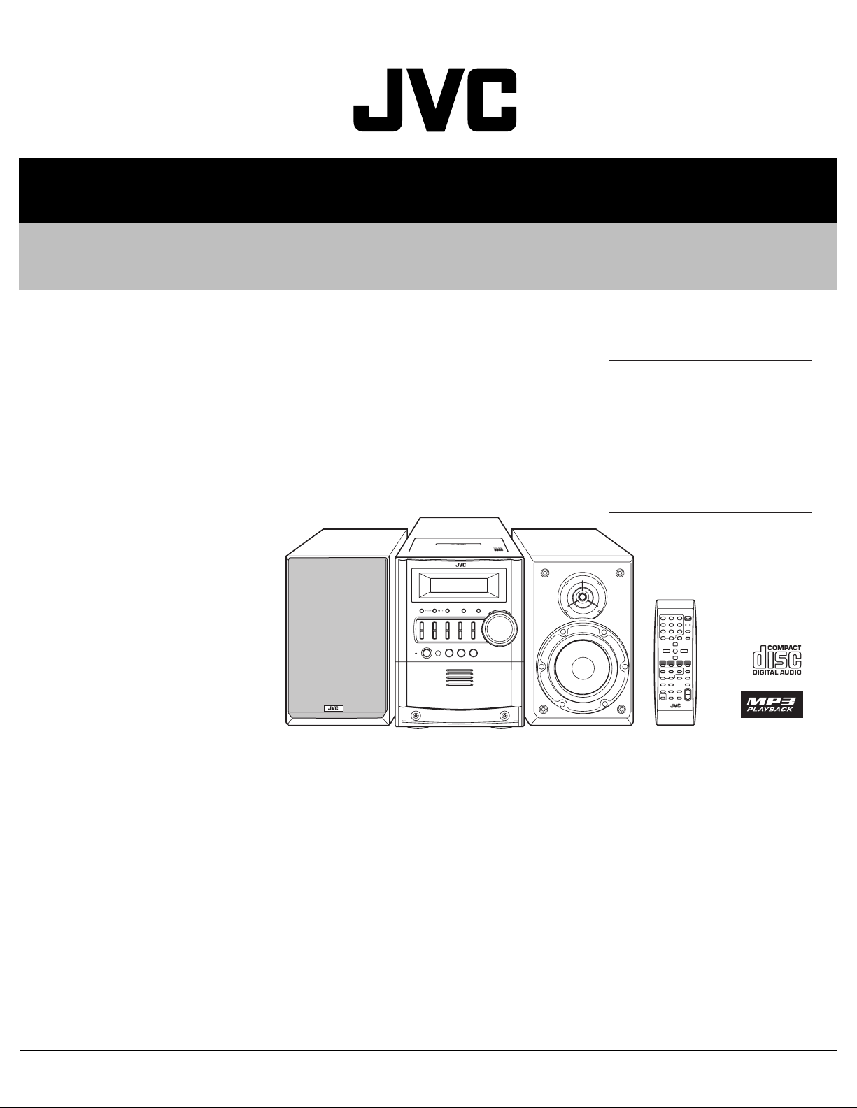
MICRO COMPONENT SYSTEM
MB43120058
UX-G5
Area suffix
A ------------------------ Australia
US ------------------------ Singapore
UP ----------------------------- Korea
UT ---------------------------- Taiwan
UW ----------- Brazil,Mexico,Peru
UY ------------------------ Argentina
UJ ---------------------- U.S.Military
CA-UXG5 SP-UXG5SP-UXG5
Lead free solder used in the board (material : Sn-Ag-Cu, melting point : 219 Centigrade)
TABLE OF CONTENTS
1 PRECAUTION. . . . . . . . . . . . . . . . . . . . . . . . . . . . . . . . . . . . . . . . . . . . . . . . . . . . . . . . . . . . . . . . . . . . . . . . . 1-3
2 SPECIFIC SERVICE INSTRUCTIONS . . . . . . . . . . . . . . . . . . . . . . . . . . . . . . . . . . . . . . . . . . . . . . . . . . . . . . 1-4
3 DISASSEMBLY . . . . . . . . . . . . . . . . . . . . . . . . . . . . . . . . . . . . . . . . . . . . . . . . . . . . . . . . . . . . . . . . . . . . . . . 1-5
4 ADJUSTMENT . . . . . . . . . . . . . . . . . . . . . . . . . . . . . . . . . . . . . . . . . . . . . . . . . . . . . . . . . . . . . . . . . . . . . . . 1-15
5 TROUBLESHOOTING . . . . . . . . . . . . . . . . . . . . . . . . . . . . . . . . . . . . . . . . . . . . . . . . . . . . . . . . . . . . . . . . . 1-18
COPYRIGHT © 2005 Victor Company of Japan, Limited
No.MB431
2005/8
Page 2

SPECIFICATION
Amplifier section Output Power 100 W (50 W+50 W) at 6 Ω (10% THD)
Speakers Impedance 6 Ω - 16 Ω
Audio Input AUX 400 mV/50 kΩ
Tuner section FM tuning range 87.50 MHz - 108.00 MHz
AM tuning range 531 kHz - 1 710 kHz (at 9 kHz)
530 kHz - 1 710 kHz (at 10 kHz)
CD player section Dynamic range 85 dB
Signal-to-noise ratio 85 dB
Wow and flutter Immeasurable
Cassette deck section Frequency response: Normal (type l) 60 Hz - 14 000 Hz
Wow and flutter 0.15% (WRMS)
General Power requirement AC 110 V - 127 V / 220 V - 240 V (adjustable with the voltage selector),
50 Hz/60 Hz
Power consumption 90 W (at operation)
0.8 W (on standby)
Dimensions (approx.) 175 mm × 232 mm × 412 mm (W/H/D)
Mass (approx.) 6.6 kg
Speakers Type 2-way Bass reflex
Speaker units Woofer 10 cm cone × 1
Tweeter 4 cm cone × 1
Impedance 6 Ω
Dimensions (approx.) 144 mm × 231 mm × 201 mm (W/H/D)
Mass (approx.) 2.0 kg each
Design and specifications are subject to change without notice.
1-2 (No.MB431)
Page 3
SECTION 1
PRECAUTION
1.1 Safety Precautions
(1) This design of this product contains special hardware and
many circuits and components specially for safety purposes. For continued protection, no changes should be made
to the original design unless authorized in writing by the
manufacturer. Replacement parts must be identical to
those used in the original circuits. Services should be performed by qualified personnel only.
(2) Alterations of the design or circuitry of the product should
not be made. Any design alterations of the product should
not be made. Any design alterations or additions will void
the manufacturers warranty and will further relieve the
manufacture of responsibility for personal injury or property
damage resulting therefrom.
(3) Many electrical and mechanical parts in the products have
special safety-related characteristics. These characteristics are often not evident from visual inspection nor can the
protection afforded by them necessarily be obtained by using replacement components rated for higher voltage, wattage, etc. Replacement parts which have these special
safety characteristics are identified in the Parts List of Service Manual. Electrical components having such features
are identified by shading on the schematics and by ( ) on
the Parts List in the Service Manual. The use of a substitute
replacement which does not have the same safety characteristics as the recommended replacement parts shown in
the Parts List of Service Manual may create shock, fire, or
other hazards.
(4) The leads in the products are routed and dressed with ties,
clamps, tubings, barriers and the like to be separated from
live parts, high temperature parts, moving parts and/or
sharp edges for the prevention of electric shock and fire
hazard. When service is required, the original lead routing
and dress should be observed, and it should be confirmed
that they have been returned to normal, after reassembling.
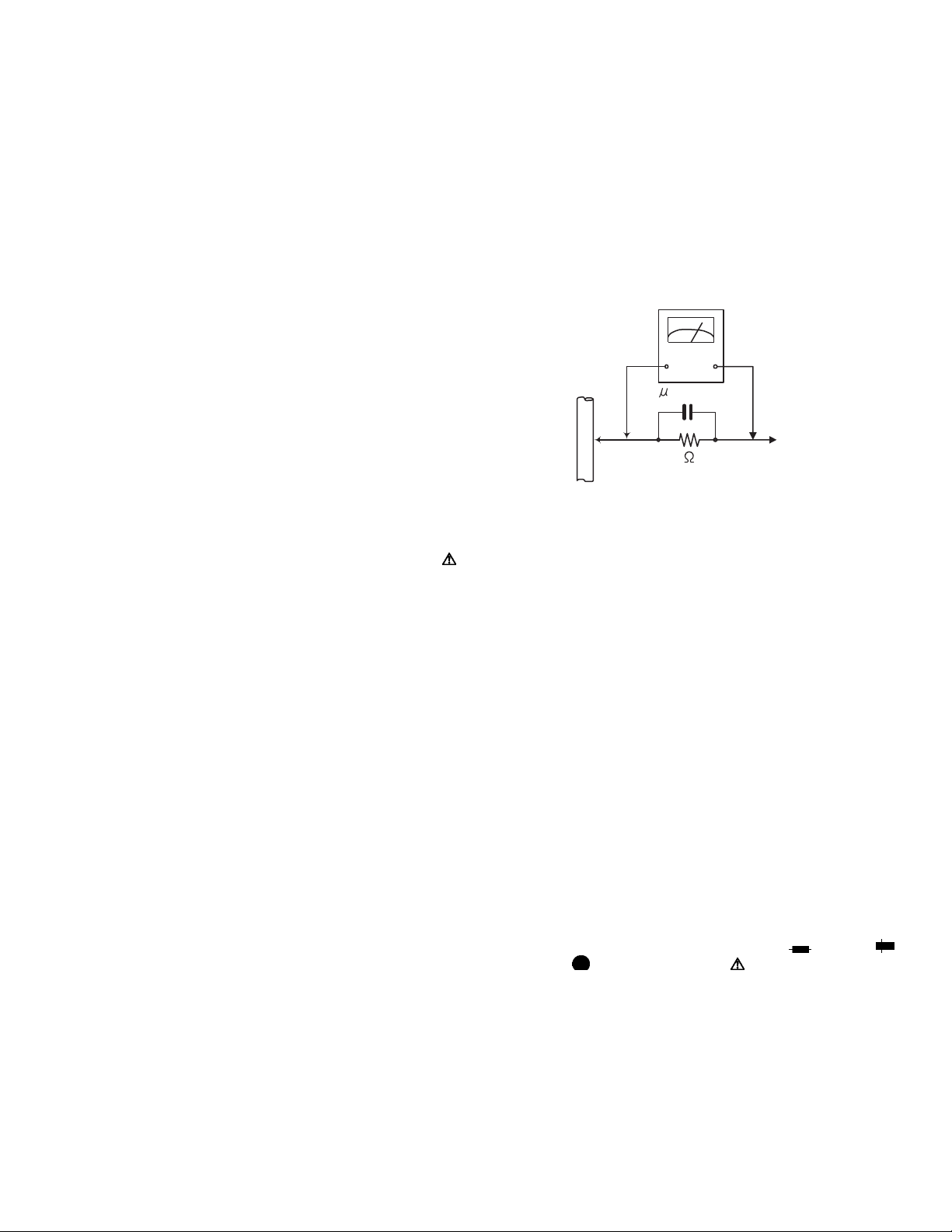
(5) Leakage shock hazard testing
After reassembling the product, always perform an isolation check on the exposed metal parts of the product (antenna terminals, knobs, metal cabinet, screw heads,
headphone jack, control shafts, etc.) to be sure the product
is safe to operate without danger of electrical shock.Do not
use a line isolation transformer during this check.
• Plug the AC line cord directly into the AC outlet. Using a
"Leakage Current Tester", measure the leakage current
from each exposed metal parts of the cabinet, particularly any exposed metal part having a return path to the
chassis, to a known good earth ground. Any leakage current must not exceed 0.5mA AC (r.m.s.).
• Alternate check method
Plug the AC line cord directly into the AC outlet. Use an
AC voltmeter having, 1,000Ω per volt or more sensitivity
in the following manner. Connect a 1,500Ω 10W resistor
paralleled by a 0.15µF AC-type capacitor between an ex-
posed metal part and a known good earth ground.
Measure the AC voltage across the resistor with the AC
voltmeter.
Move the resistor connection to each exposed metal
part, particularly any exposed metal part having a return
path to the chassis, and measure the AC voltage across
the resistor. Now, reverse the plug in the AC outlet and
repeat each measurement. Voltage measured any must
not exceed 0.75 V AC (r.m.s.). This corresponds to 0.5
mA AC (r.m.s.).
AC VOLTMETER
(Having 1000
ohms/volts,
or more sensitivity)
0.15 F AC TYPE
Place this
probe on
1500 10W
Good earth ground
1.2 Warning
(1) This equipment has been designed and manufactured to
meet international safety standards.
(2) It is the legal responsibility of the repairer to ensure that
these safety standards are maintained.
(3) Repairs must be made in accordance with the relevant
safety standards.
(4) It is essential that safety critical components are replaced
by approved parts.
(5) If mains voltage selector is provided, check setting for local
voltage.
1.3 Caution
Burrs formed during molding may be left over on some parts
of the chassis.
Therefore, pay attention to such burrs in the case of preforming repair of this system.
1.4 Critical parts for safety
In regard with component parts appearing on the silk-screen
printed side (parts side) of the PWB diagrams, the parts that are
printed over with black such as the resistor ( ), diode ( )
and ICP ( ) or identified by the " " mark nearby are critical
for safety. When replacing them, be sure to use the parts of the
same type and rating as specified by the manufacturer.
(This regulation dose not Except the J and C version)
each exposed
metal part.
(No.MB431)1-3
Page 4

SECTION 2
SPECIFIC SERVICE INSTRUCTIONS
This service manual does not describe SPECIFIC SERVICE INSTRUCTIONS.
1-4 (No.MB431)
Page 5
SECTION 3
DISASSEMBLY
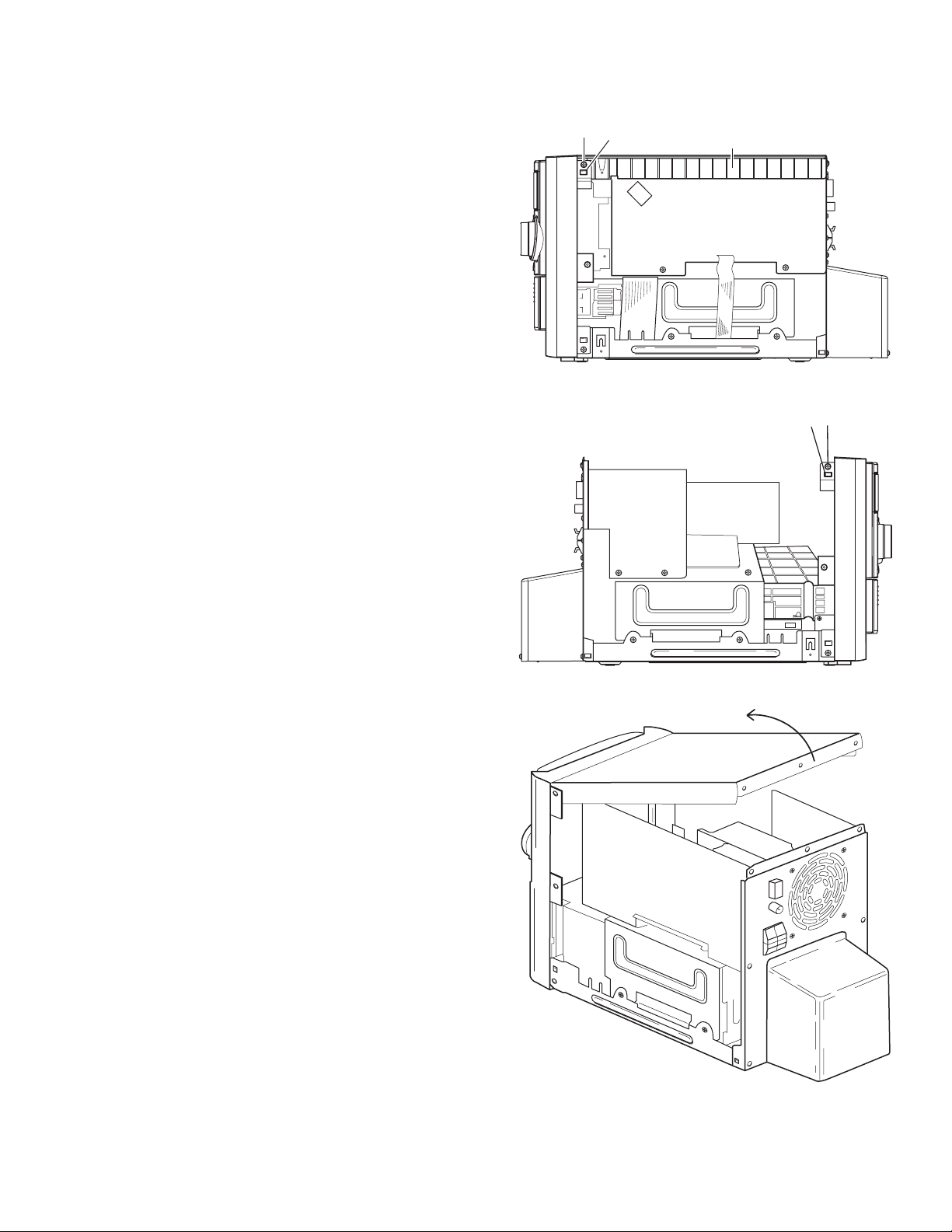
3.1 Disassembly of Right plate left plate Top cover
Replacement of the fuses and AMP TR .THMS RES. Transistor. 7808 IC.
3.1.1 Replacing the fuses
(See Fig.1)
• Prior to performing the following procedure, remover right
plate, left plate, top cover.
(1) Replace the fuses inside.
Caution:
Be sure to use fuses with the specified
3.1.2 Replacing the AMP TR
(See Fig.2)
• Prior to performing the following procedure, remove the right
plate, left plate, top cover.
(1) Remove the four screws A from the heat sink between
AMP TR four.
(2) Remove the solder fixing the AMP TR.
FUSE
Fig.1
B
3.1.3 Replacing the THMS RES
(See Fig.2)
• Prior to performing the following procedure, remove right plate,
left plate, top cover.
(1) Remove the one screw B from heat sink.
(2) Remove the solder fixing THMS RES.
3.1.4 Replacing the 7808 IC
(See Fig.3)
(1) Remove the two screws D from heat sink.
(2) Remove the solder fixing transistor.
THMS RES
Fig.2
D
A
(TR)
Fig.3
(No.MB431)1-5
Page 6
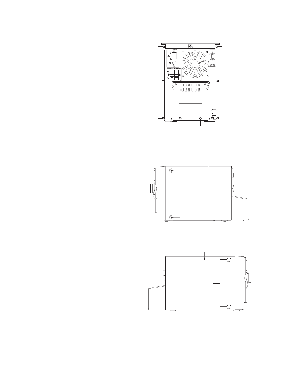
3.1.5 Removing the transformer cover
r
(See Fig.4)
(1) Remove the ten screws E from top cover.
(2) Take off transformer cover from rear plate.
E
3.1.6 Removing the Right plate
(See Fig.5)
(1) Remove the two screws F.
(2) Take off right plate from main body.
E
SPEAKERS IMPEDANCE:6 16
E
Transforme
cover
E
Fig.4
Right plate
F
3.1.7 Removing the Left plate
(See Fig.6)
(1) Remove the two screws G.
(2) Take off left plate from main body.
1-6 (No.MB431)
Fig.5
Left plate
G
Fig.6
Page 7
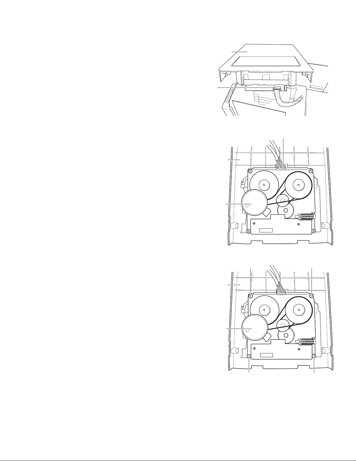
3.1.8 Removing the TOP COVER
(See Fig.7 to 9)
(1) Remove the two screws H1 (See Fig.7, 8).
(2) Disengage the claws H2 on both side of the front cabinet
(See Fig.7, 8).
(3) Rotate top cover and let's away from main body (See
Fig.9).
Caution:
When you rotate top cover, must to slow raise, Don't to destroy
the two claws of front cabinet.
H1
H2
Top cover
Fig.7
H2
H1
Fig.8
Fig.9
(No.MB431)1-7
Page 8
3.1.9 Removing the main board
(See Fig.10 to 13)
(1) Remove the two screws J1. (See Fig.10)
(2) Disconnect the FFC cable J2 from the connector CN661 on
main board. (See Fig.10)
(3) Disconnect the FFC cable J3 from the connector CN402
main board. (See Fig.11)
(4) Disconnect the FFC cable J4 from the connector CN681
main board. (See Fig.12)
(5) Remove main board from AMP board after disconnect the
connector J319
and CN601. (See Fig.13)
on
on
J1 J1
J2
Fig.10
J3
J5
Fig.11
J4
Fig.12
1-8 (No.MB431)
Fig.13
Page 9
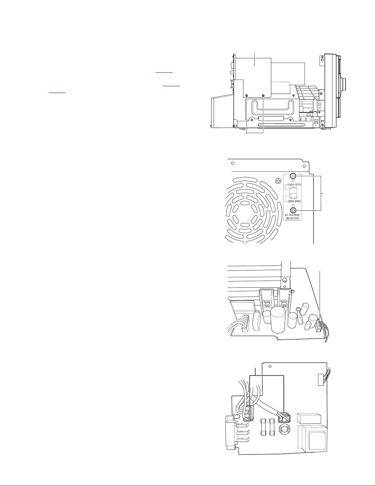
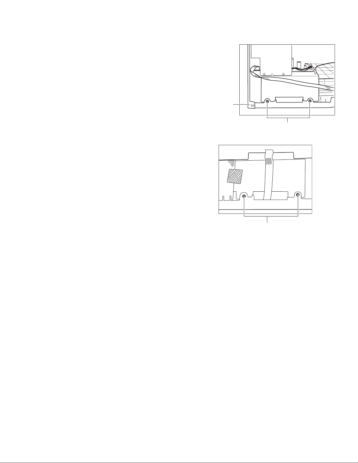
3.1.10 Removing the Power board
(See Fig.14 to 16)
(1) Remove the two screws K1 from CD MECH cover and
power board. (See Fig.14)
(2) Remove the two screws K1 from rear plate and power
board. (See Fig.14-1)
(3) Disconnect the wire K2 from the connector CN102
AMP board. (See Fig.15)
(4) Disconnect the two wire K3 from the connector CN901
. (See Fig.16)
CN902
on the
Power board
and
K1
Fig.14
k1
K3
Fig.14-1
K2
Fig.15
Fig.16
(No.MB431)1-9
Page 10
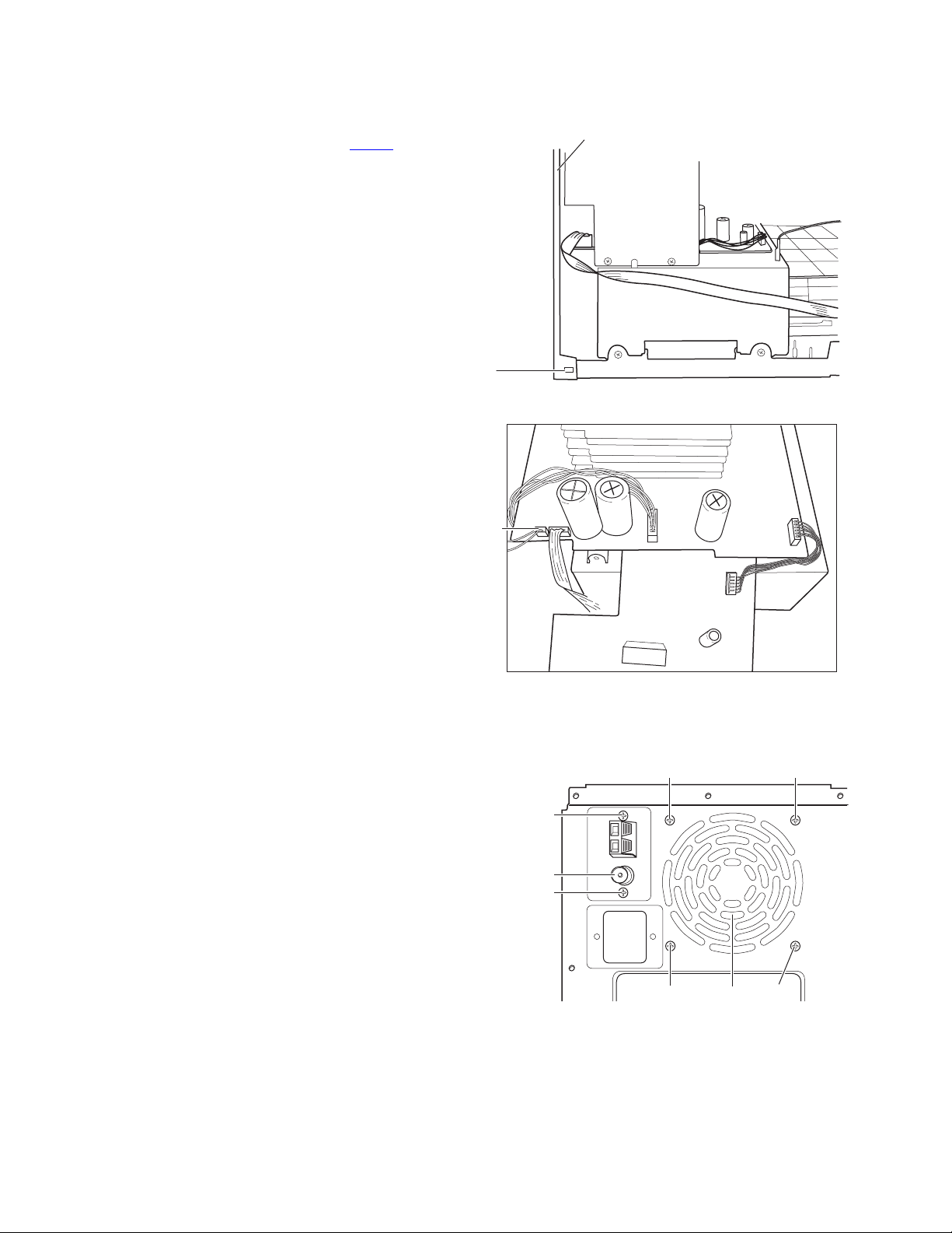
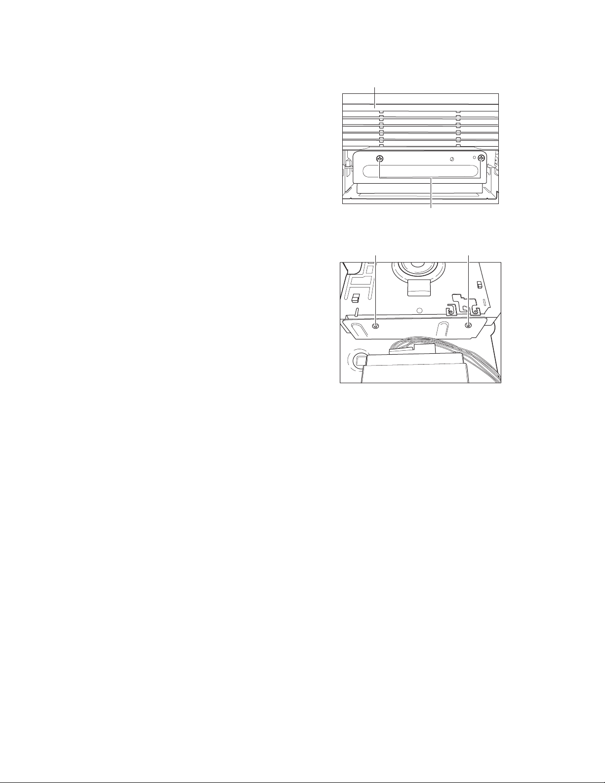
3.1.11 Removing the Rear plate assembly
(See Fig.17 to 18)
(1) Disengage the claws I1 on both sides of bottom plate. (See
Fig.17)
(2) Disconnect the wire I2 from the connector CN105 on the
AMP board. (See Fig.18)
Rear plate assembly
I1
Fig.17
3.1.12 Removing the fan
(See Fig.19)
(1) Removing the four screws M2.
3.1.13 Removing the Tuner pack
(See Fig.19)
(1) Removing the two screws M1.
I2
M1
Tuner pack
M1
Fig.18
M2
M2
1-10 (No.MB431)
M2 Fan
Fig.19
M2
Page 11
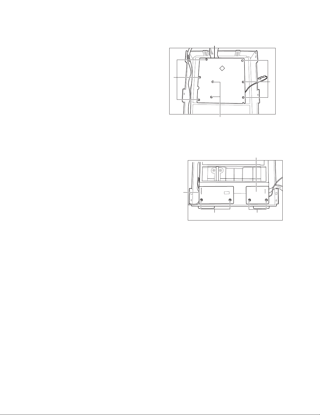
3.1.14 Removing the cassette machine from top cover
(See Fig.20 to 22)
(1) Disconnect the wire E1 from connector of the cassette ma-
chine. (See Fig.20)
(2) Disconnect the wire E2 from connector of the cassette ma-
chine. (See Fig.21)
(3) Remove the four screws E3 from top cover. (See Fig.22)
(4) Take out cassette machine.
TOP COVER
E1
Fig.20
E2
TOP COVER
CASSETTE
MECHA
TOP COVER
CASSETTE
MECHA
Fig.21
E3E3
Fig.22
E3E3
(No.MB431)1-11
Page 12
3.1.15 Removing the key board
A
(See Fig.23)
(1) Remove the eight screws P from the front cabinet and the
key board.
Key board
3.1.16 Removing the AUX board
(See Fig.24)
(1) Remove the two screws Q from the front cabinet and the
aux board.
3.1.17 Removing the phones board
(See Fig.24)
(1) Remove the two screws R from the front cabinet and the
phones board.
P
ux board
P
Fig.23
Q
Fig.24
P
Phones board
R
1-12 (No.MB431)
Page 13
3.1.18 Removing the CD MECH COVER
(See Fig.25, 26)
(1) Remove the four screws S.
CD Mech Cover
S
Fig.25
S
Fig.26
(No.MB431)1-13
Page 14
3.1.19 Removing the CD MECH Assembly
(See Fig.27, 28)
(1) Remove the two screws T from the CD MECH-F and CD
MECHANISM assembly. (See Fig.27)
(2) Remove the two screws T from the CD MECH-B and CD
MECHANISM assembly. (See Fig.28)
(3) Take out CD MECHANISM assembly from the CD MECH-
F between the CD MECH-B.
CD MECH Assembly
T
Fig.27
T T
Fig.28
1-14 (No.MB431)
Page 15

SECTION 4
ADJUSTMENT
4.1 Measuring instructions required for adjustment
• AM signal generator
• FM signal generator
• Inter medicate frequency sweep generator
• FM stereo signal generator
• Low-frequensy oscillator (osillation frequency 50 Hz - 20 kHz, 0 dB output with 600 Ω impedance)
• Attenuator (600 Ω impedance)
• Electoronic voltmeter
• Distortion meter
• Torque gauge (cassette for CTG-N)
• Wow & flutter meter
• Frequency counter meter
4.2 Test tape
• Playback tape
VT712 (tape speed, wow flutter)
VT724 (reference level)
VT703L (head azimuth)
VT738 (frequency responce)
• Recording tape
AC225 (type I)
• Power supply voltage
AC220V - 240V 50Hz
4.3 Measuring instruments
• Radio section
FM : 1 kHz, 22.5kHz deviation
FM stereo : 1 kHz, 67.5 kHz deviation, pilot signal 7.5 kHz
AM : 1 kHz, 30% modulation
Reference output : 0 dB (1 V) 4 Ω
Headphone output : -10 dB (0.1V) 32 Ω
4.4 Amplifier section
• Reference output : Speaker output 0 dB (1 V) / 4 Ω
Headphone output -10 dB (0.1 V) / 32 Ω
4.5 CD section
• Test disc : CTS-1000 (JVC)
TCD-731R (A-BEX)
TCD-712R (A-BEX)
TCD-785 (A-BEX)
(No.MB431)1-15
Page 16

4.6 Cassette amplifier section
Item Measuring condition Check and adjustment procedure Standard value Adjusting part
Head azimuth
adjustment
Test tape : VT703
Signal output terminal :
PHONES
(with 32 ohm load)
1.Plyback the test tape VT703.
2.Adjust the head azimuth adjusting screw
so that the phase difference between the
R and L channels is minimized at an
output level that is within +/- 2dB of the
maximum output level.
After this adjustment, lock the head
azimuth adjusting screw with screw
sealant to cover more than a half of the
screw head.
3.When the head azimuth is maladjusted,
correct it with the head azimuth adjusting
screw.
Output level :
within +/-2dB
of maximum
output level
Phase defference
L and R channels:
minimum
Head azimuth
adjusting screw
(to be used only
after head replacement)
Tape speed
and
wow/flutter
check and
adjustment
PB frequency
responce
check
Bias frequency
check
REC and PB
frequency
responce
adjustment
Test tape : VT712
Signal output terminal :
PHONES
(with 32 ohm load)
Test tape : VT738
Signal output terminal :
PHONES
(with 32 ohm load)
Test tape : normal
Signal output terminal :
Casssette R/P head
Test tape : AC225
Signal input : FM 22.5
dev, 60dBu with
emphasis
Signal output terminal :
PHONES
(with 32 ohm load)
1.Plyback the test tape VT712 by the end
of position.
2.Connect a frequency counter and check
that it reads between 2940 and 3090 Hz.
If not, adjust the frequenct with the motor
semifixed resistor.
3.Check that the wow / flutter is 0.38%
(unweighted).
Playback the test tape VT738 while confirming that deviation between the 1 kHz
signal and 8 kHz signal should be
0 (+3 to -6) dB.
Set the TUNER or CD function and with
TAPE to record. Check to see if the
frequency at the measuring point (R335 or
R336) is 60 kHz +/-1 kHz if not adjust T360
until the frequency counter indicates
60 kHz +/- 1 kHz.
At TUNER, set the BAND to the FM
position, and record the reference 1 kHz
signal and 8 kHz signal altemately
repeatedly. While playing back the
recorded signal differ from that of the 1 kHz
signal by within 0 (+3 to 6) dB.
2940 to 3090 Hz
within 0.38%
(unweighted)
deviation between
1 kHz and 8 kHz :
0 (+3 to -6) dB.
Level difference
between REC and
PB : within 0
(+3 to 6) dB
Tape speed :
motor semifixed
resistor
check only
L203
4.7 Tuner section
Item Measuring condition Check and adjustment procedure Standard value Adjusting part
AM IF
adjustment
AM tracking
adjustment
Tuner 114 kHz
filter the waves
adjustment
1-16 (No.MB431)
Signal input : Loop
antenna
Signal output : IC201
pin 18
Signal input : Loop
antenna
Signal output : PHONES
(with 32 ohm load)
Signal input : IC101
pin 19
Signal output : IC101
pin 18
1.Set the intermediate frequency sweep
generator to AM 450 kHz.
2.Adjust the T203 from maximum and
center output.
1.Set the TUNER at 522 kHz adjust T201
until the test pin of R245 voltage at
1.55 V +/- 0.1 V.
2.Set the TUNER at 1629 kHz, check the
pin of R245 voltage at 8.4 V +/- 6V.
3.Set the TUNER ang S/G at 612 kHz,
adjust T202 for maximum output.
4.Set the TUNER and S/G at 1404 kHz,
adjust T201 for maximum output.
5.Repwat the above step 3 and 4.
1.Set the unit in standby mode. Input 114
kHz signal to IC101 pin 19.
2.Adjust the T204 for output voltage
minimum.
T203
T201
R245
TC201
T204
Page 17

4.8 Location of adjusting parts
Cassette mechanism section
Main board assembly
(AM RF)
T202
Tape speed adj.
(AM IF)
T203
-
+
CASSETTE
MOTOR
TC201
R245
(AM VT)
(AM RF)
T201
(AM OSC)
T204
(114 kHz)
T360
(BIAS FREQUENCY)
(No.MB431)1-17
Page 18

SECTION 5
TROUBLESHOOTING
This service manual does not describe TROUBLESHOOTING.
1-18 (No.MB431)
Page 19

(No.MB431)1-19
Page 20

Victor Company of Japan, Limited
AV & MULTIMEDIA COMPANY AUDIO/VIDEO SYSTEMS CATEGORY 10-1,1chome,Ohwatari-machi,Maebashi-city,371-8543,Japan
(No.MB431)
Printed in Japan
VPT
Page 21

SCHEMATIC DIAGRAMS
MICRO COMPONENT SYSTEM
UX-G5
CD-ROM No.SML200508
CA-UXG5 SP-UXG5SP-UXG5
Area suffix
A ------------------------ Australia
US ------------------------ Singapore
UP ----------------------------- Korea
UT ---------------------------- Taiwan
UW ----------- Brazil,Mexico,Peru
UY ------------------------ Argentina
UJ ---------------------- U.S.Military
Lead free solder used in the board (material : Sn-Ag-Cu, melting point : 219 Centigrade)
Contents
Block diagram
Standard schematic diagrams
Printed circuit boards
COPYRIGHT 2005 Victor Company of Japan, Limited.
2-1
2-2
2-6 to 11
No.MB431SCH
2005/8
Page 22

In regard with component parts appearing on the silk-screen printed side (parts side) of the PWB diagrams, the
parts that are printed over with black such as the resistor ( ), diode ( ) and ICP ( ) or identified by the " "
mark nearby are critical for safety.
Page 23

Block diagram
PICKUP ASS'Y
TRA MECHA ASS'Y
LOADER ASS'Y
TRAY MOTOR
E F
A B C D
RF & SERVO
AMP
SIL9226
DRAM
BR93L56RF
CD CONTROL
MICON
MN101C61G
FWD,REV
DIGITAL SERVO &
AIGNAL PROCESSOR
S5L9279
TRP
FOP
TRVP
SPOUT
DRIVER
IP4001S
I/O
DIGITAL OUTPUT
ANALOG OUTPUT
DRAM FOR MP3
K4S161622H
TRACKING COIL
FOCUS COIL
SPINDLE MOTOR
FEED MOTOR
LCD DISPLAY
KEY CONTROL
TUNER MODULE
FM/AM
ST LED
9V
TUNER-L
GND
TUNER-R
CEI
DATA IN
CLK1
DATA OUT
D-GND
RDS CLK
RDS DATA
L/R
TAPE
AUX IN
47K IMPEDANCE
FAN
VOLTAGE SUPPLY
AC IN
BACKUP
PT
SUB-TRANS 1.5W
PREMARY FUSE
VOLTAGE SUPPLY
110/127
220/240
AC selector
DISPLAY O/P
SYSTEM MICON
MAIN PT
S3C825A
TU CONT.
CD L/R
TU L/R
TAPE L/R
FUNC IC
BD388IFV
VOLUME
FUNCTION SW
TAPE PRE-AMP
AUX L/R
BA455B
AHB PRO CONTROL
L/R CH
Tr SD1889&SB1340
50W X 2 AMP
+ / -24V
5V REGULATOR
6 OHM
HP OUT
32 OHM IMPEDANCE
2-1
Page 24

Standard schematic diagrams
Main section
2-2
Page 25

Amp section
!
Parts are safety assurance parts.
When replacing those parts make
sure to use the specified one.
2-3
Page 26

CD section
2-4
Page 27

FL & Primary section
Parts are safety assurance parts.
When replacing those parts make
sure to use the specified one.
2-5
Page 28

Printed circuit boards
Main board
Lead free solder used in the board (material : Sn-Ag-Cu, melting point : 219 Centigrade)
(forward side)
2-6
Page 29

Main board
Lead free solder used in the board (material : Sn-Ag-Cu, melting point : 219 Centigrade)
(reverse side)
2-7
Page 30

Amp board
Lead free solder used in the board (material : Sn-Ag-Cu, melting point : 219 Centigrade)
(forward side) (reverse side)
2-8
Page 31

CD board
Lead free solder used in the board (material : Sn-Ag-Cu, melting point : 219 Centigrade)
(forward side) (reverse side)
2-9
Page 32

Front board
Lead free solder used in the board (material : Sn-Ag-Cu, melting point : 219 Centigrade)
(forward side) (reverse side)
2-10
Page 33

Trans board
Lead free solder used in the board (material : Sn-Ag-Cu, melting point : 219 Centigrade)
2-11
Page 34

Victor Company of Japan, Limited
AV & MULTIMEDIA COMPANY AUDIO/VIDEO SYSTEMS CATEGORY 10-1,1chome,Ohwatari-machi,Maebashi-city,371-8543,Japan
(No.MB431SCH)
Printed in Japan
VPT
Page 35

PARTS LIST
[ UX-G5 ]
* All printed circuit boards and its assemblies are not available as service parts.
Area suffix
A ------------------------- Australia
US ---------------------- Singapore
UP ---------------------------- Korea
UT --------------------------- Taiwan
UW ---------- Brazil,Mexico,Peru
UY ----------------------- Argentina
UJ --------------------- U.S.Military
MB431
- Contents -
Exploded view of general assembly and parts list (Block No.M1)
CD mechanism assembly and parts list (Block No.MB)
Electrical parts list (Block No.01~06)
Packing materials and accessories parts list (Block No.M3)
3- 2
3- 5
3- 7
3-14
3-1
Page 36

Exploded view of general assembly and parts list
8
Block No.
M
M
1
M
14
20
20
24
25
23
Power trans.
board
16
19
16
18
17
1
9
15
13
8
7
A
23
21
F901
71
B
Front board
F902
72
38
23
28
37
28
23
23
2
2
2
2
2
2
47
2
23
B
2
3-2
54
57
53
55
56
23
62
63
10
6
5
11
11
13
11
12
2
4
3
64
65
Dusb board
2
68
2
Dhp
board
2
64
2
58
61
60
59
2
64
58
66
67
68
68
CD board
2
Page 37

31
30
A
23
42
28
34
29
41
35
43
44
45
45
45
44
44
45
70
44
44
28
28
38
23
28
23
39
36
28
28
33
27
32
Amp.
board
3
28
44
B
44
Main board
44
46
7
53
55
56
23
56
23
54
12
54
52
23
49
51
23
49
50
20
20
3-3
Page 38

General Assembly
Symbol No. Part No. Part Name Description Local
1 BI1080670302V1 FRONT CABINET NO USB
2 BIBT000418 SCREW 2.6 XL8(x23)
3 BI1081770101X1 SLIDE BLOCK
4 BI1080690201V1 CD DOOR
5 BI1080770101V1 BOTTOM LENS R
6 BI1080780101V1 BOTTOM LENS L
7 BI1080750101V1 TOP LENS R
8 BI1080800101V1 VOLUME KNOB ABS-T700 94HB
9 BI1080820101V1 KEY PANEL
10 BI202904010101 CD DOOR SPRING
11 BIKT000606B3 SCREW 3xL6(x4)
12 BI302197010101 RUBBER FOOT (x4)
13 BI302193010101 CD DOOR RUBBER (x2)
14 BI1080760101V1 TOP LENS L
15 BI1080720301V1 WINDOW LENS
16 BIKT000606 SCREW (x2)
17 BI1080810201V1 FUNCTION KEY
18 BI2702191V LCD LCD1 TCM-4217
19 CM04115 LED D352 BI680FSG505L
20 BIRT000608B1W SCREW 3xL8(x4)
21 BI1080840101V1 LCD HOLDER
23 BIBT000604S3 SCREW (x15)
24 BI2028960101X2 LEFT PLATE
25 BI3022090102X1 PC PLATE
27 BI1098410101V1 LOCK HLDR
28 BIRT000611B3 SCREW 3 X L8 B-TYPE(x13)
29 BI250101001000 CASSETTE MECH
30 BI1080680102V1 TOP COVER CASSETTE
31 BI1080710101V1 CASSETTE DOOR
32 BI202408010101 SPRING LOCKER
33 BI1098400101V1 CASS LOCK LEVER
34 BI300924010101 DAMPER
35 BI202905010101 CASSETTE SPRING
36 BI2029350101W1 HEATSINK BKT B
37 BI2029340101W1 HEATSINK BKT F
38 BI202903010201 HEATSINK
39 BI2029330101X2 HEAT RESISTOR BKT
41 BT2400241V DC FAN DC12V
42 BIZ25094901VV TUNER PACK
43 BI2028950202X2 REAR PLATE
44 BIRM000603S3 SCREW 3 X L6 S-TYPE(x12)
45 BIRT000617B3 SCREW 3 X L10 B-TYPE(x10)
46 BI1080790101V1 TRANS COVER
47 BI2029000101X2 CD MECH COVER
49 BIPMW001101S3 SCREW 4.0XL6 METAL(x4)
50 BI2028970101X2 RIGHT PLATE
51 BI211011136001 POWER TRANS
52 BI2028990101X2 CD MECH BKT
53 BI2028940101X2 BOTTOM PLATE
54 BIRT000603P3 SCREW (x4)
55 BI2028980101X2 CD MECH HOLDER
56 BIRT000604S3 SCREW RT 3X6(x6)
57 BI251051000300V 5CD CHANGER
58 BI301942010101 CUSHION RUBBER (x2)
59 BI1081030101V1 CD CHUCK
60 BI202930010101 CD MAGNET
61 BI2029060101X2 CD CHUCK PLATE
62 BI1080740101V1 LENS
63 BI1080730101V1 POWER LENS
64 BI300856010101 WASHER (x4)
65 BI301943010101 CUSHION RUBBER (x2)
66 BI251011003200V CD MECHANISM
67 BI1080830101V1 CD MECH HOLDER
68 BIBT000405S3 SCREW (x3)
70 BI1401661V POWER CORD A
70 BI1401471V POWER CORD UP
70 BI1401551V POWER CORD UT
70 BI1401741X POWER CORD UJ,US,UW
70 BI1401521V POWER CORD UY
71 BI402891 FUSE F901 1.6A 250V
72 BI402861X FUSE F902 800mA 250V
Block No. [M][1][M][M]
3-4
Page 39

CD mechanism assembly and parts list
Block No.
M
6
M
M
B
14
10
1
7
10
3
11
8
9
2
5
4
12
13
The parts without symbol number are not service.
3-5
Page 40

CD mechanism
Symbol No. Part No. Part Name Description Local
1 BIAJ7000601E CHASSIS
2 BIAJ6600601G GEAR COVER
3 BIAJ6600601D GEAR A
4 BIAJ6600601B GEAR B
5 BIAJ6600601F GEAR C
6 BIAJ7000601A SHAFT
7 BISOHAAN PICK UP
8 BIAJ3100601B SPINDLE MOTOR
9 BIAJ3100601A FEED MOTOR
10 BIAJ6000601D SCREW M2XL3(x4)
11 BI3409000174 LEAF SWITCH
12 BIAJ4100601E SUB PCB
13 BIAJ3700601A CONNECTOR
14 BIAJ7500601K TURN TABLE
Block No. [M][B][M][M]
3-6
Page 41

Electrical parts list
Main board
Block No. [0][1]
Symbol No.
IC401 S3C825A IC BI118131
IC402 PST3429UL IC BI117161
IC501 BA4558F IC BI103952
IC601 BD3881FV IC BI112721V
Q301 2SK2158 F.E.T BI2SK2158A015V1
Q302 2SK2158 F.E.T BI2SK2158A015V1
Q303 2SK2158 F.E.T BI2SK2158A015V1
Q304 DTA124EK DIGI TRANSISTOR BI2DTA124EKA008
Q306 DTC124EKA DIGI TRANSISTOR BI2DTC124EKA018
Q307 2SA1235F TRANSISTOR BI2SA1235FA012H
Q308 2SA1235F TRANSISTOR BI2SA1235FA012H
Q311 2SC3052 TRANSISTOR BI2SC3052FA013H
Q312 2SC5343 TRANSISTOR BI2SC5343GP0000
Q313 2SC5343 TRANSISTOR BI2SC5343GP0000
Q331 KTA1273Y TRANSISTOR BI2KTA1273YP000
Q332 DTC114TK DIGI TRANSISTOR BI2DTC114TKA011
Q333 KTA1273Y TRANSISTOR BI2KTA1273YP000
Q334 DTC114TK DIGI TRANSISTOR BI2DTC114TKA011
Q335 2SC5343 TRANSISTOR BI2SC5343GP0000
Q336 2SC3052 TRANSISTOR BI2SC3052FA013H
Q401 DTC114YK DIGI TRANSISTOR BI2DTC114YKA018
Q402 2SC3052 TRANSISTOR BI2SC3052FA013H
Q403 2SC3052 TRANSISTOR BI2SC3052FA013H
Q404 2SC3052 TRANSISTOR BI2SC3052FA013H
Q404 DTA124EK DIGI TRANSISTOR BI2DTA124EKA008
Q405 2SA1980 TRANSISTOR BI2SA1980GP0000
Q501 KTC3199GR TRANSISTOR BI2KTC3199GP000
Q502 KTC3199GR TRANSISTOR BI2KTC3199GP000
Q602 2SC3052 TRANSISTOR BI2SC3052FA013H
Q603 2SC3052 TRANSISTOR BI2SC3052FA013H
Q683 KTA1267GR TRANSISTOR BI2KTA1267GP00
Q684 2SC3052 TRANSISTOR BI2SC3052FA013H
D301 1SS133 FR DIODE BI31SS133M000V7
D331 1SS133 FR DIODE BI31SS133M000V7
D332 1SS133 FR DIODE BI31SS133M000V7
D401 1SS133 FR DIODE BI31SS133M000V7
D402 1SS133 FR DIODE BI31SS133M000V7
D403 1SS133 FR DIODE BI31SS133M000V7
D404 1SS133 FR DIODE BI31SS133M000V7
D405 1SS133 FR DIODE BI31SS133M000V7
D406 1SS133 FR DIODE BI31SS133M000V7
D407 1SS133 FR DIODE BI31SS133M000V7
D421 1SS133 FR DIODE BI31SS133M000V7
D423 1SS133 FR DIODE BI31SS133M000V7
D424 1SS133 FR DIODE BI31SS133M000V7
D501 1SS133 FR DIODE BI31SS133M000V7
D502 1SS133 FR DIODE BI31SS133M000V7
D601 ISS355 DIODE BI31SS355A0077
D602 ISS355 DIODE BI31SS355A0077
D603 1SS133 FR DIODE BI31SS133M000V7
C301 BICC472500KA04 C CAPACITOR 4700pF 50V
C302 BICC472500KA04 C CAPACITOR 4700pF 50V
C303 BICC221500JA04 C CAPACITOR 220pF 50V
C311 BICC102500KA04 C CAPACITOR 1000pF 50V
C312 BICC102500KA04 C CAPACITOR 1000pF 50V
C313 BICC561500JA04 C CAPACITOR 560P 50V
C314 BICM562101KP01 M CAPACITOR 5600pF 100V
C315 BICE227100MP01 E CAPACITOR 220uF 10V
C316 BICC103500KA04 C CAPACITOR 0.01uF 50V
C317 BICC272500KA04 C CAPACITOR 2700pF
C318 BICC272500KA04 C CAPACITOR 2700pF
C319 BICC272500KA04 C CAPACITOR 2700pF
C331 BICE476160MP01 E CAPACITOR 47uF 16V
C332 BICE476160MP01 E CAPACITOR 47uF 16V
C333 BICE476160MP01 E CAPACITOR 47uF 16V
C334 BICC104500KA04 C CAPACITOR 0.1uF 50V
C335 BICC104500KA04 C CAPACITOR 0.1uF 50V
C336 BICE227160MP01 E CAPACITOR 220uF 16V
C401 BICC104500ZA04 C CAPACITOR 0.1uF 50V
Part No. Part Name Description Local
Symbol No.
C402 BICE107160MP01 E CAPACITOR 100uF 16V
C403 BICC150500JA04 C CAPACITOR 15pF 50V
C404 BICC330500JA04 C CAPACITOR 33pF 50V
C405 BICC101500JA04 C CAPACITOR 100pF 50V
C406 BICC104500ZA04 C CAPACITOR 0.1uF 50V
C407 BICC104500ZA04 C CAPACITOR 0.1uF 50V
C408 BICE226160MP01 E CAPACITOR 22uF 16V
C409 BICC104500ZA04 C CAPACITOR 0.1uF 50V
C411 BICC220500JA04 C CAPACITOR 22pF 50V
C412 BICC220500JA04 C CAPACITOR 22pF 50V
C413 BICE477063MP01 E CAPACITOR 470uF 6.3V
C414 BICE477063MP01 E CAPACITOR 470uF 6.3V
C415 BICE107100MP01 E CAPACITOR 100uF 10V
C416 BICC222500KA04 C CAPACITOR 2200pF 50V
C417 BICC104500KA04 C CAPACITOR 0.1uF 50V
C418 BICC105100ZA04 C CAPACITOR 1uF 10V
C421 BICC104500ZA04 C CAPACITOR 0.1uF 50V
C422 BICC330500JA04 C CAPACITOR 33pF 50V
C423 BICC330500JA04 C CAPACITOR 33pF 50V
C424 BICC330500JA04 C CAPACITOR 33pF 50V
C425 BICC330500JA04 C CAPACITOR 33pF 50V
C426 BICC220500JA04 C CAPACITOR 22pF 50V
C501 BICE107160MP01 E CAPACITOR 100uF 16V
C502 BICE107160MP01 E CAPACITOR 100uF 16V
C503 BICC104500ZA04 C CAPACITOR 0.1uF 50V
C504 BICC104500ZA04 C CAPACITOR 0.1uF 50V
C505 BICM124101KP01 M CAPACITOR 0.12uF 100V
C506 BICM124101KP01 M CAPACITOR 0.12uF 100V
C507 BICE107160MP01 E CAPACITOR 100uF 16V
C508 BICE107160MP01 E CAPACITOR 100uF 16V
C509 BICE475500MP01 E CAPACITOR 4.7uF 50V
C510 BICE475500MP01 E CAPACITOR 4.7uF 50V
C511 BICE475500MP01 E CAPACITOR 4.7uF 50V
C601 BICC470500JA04 C CAPACITOR 47pF 50V
C602 BICC470500JA04 C CAPACITOR 47pF 50V
C603 BICE226160MP01 E CAPACITOR 22uF 16V
C604 BICE226160MP01 E CAPACITOR 22uF 16V
C605 BICC103500KA04 C CAPACITOR 0.01uF 50V
C606 BICC103500KA04 C CAPACITOR 0.01uF 50V
C607 BICC181500JA04 C CAPACITOR 180pF
C608 BICC181500JA04 C CAPACITOR 180pF
C609 BICC122500KA04 C CAPACITOR 1200pF 50V
C610 BICC122500KA04 C CAPACITOR 1200pF 50V
C611 BICE225500MP01 E CAPACITOR 2.2uF 50V
C612 BICE225500MP01 E CAPACITOR 2.2uF 50V
C625 BICC103500KA04 C CAPACITOR 0.01uF 50V
C626 BICC103500KA04 C CAPACITOR 0.01uF 50V
C627 BICC682500KA04 C CAPACITOR 6800pF 50V
C628 BICC682500KA04 C CAPACITOR 6800pF 50V
C631 BICC822500KA04 C CAPACITOR 8200pF 50V
C632 BICC822500KA04 C CAPACITOR 8200pF 50V
C633 BICC101500JA04 C CAPACITOR 100pF 50V
C634 BICC104500ZA04 C CAPACITOR 0.1uF 50V
C635 BICC104500ZA04 C CAPACITOR 0.1uF 50V
C636 BICE227100MP01 E CAPACITOR 220uF 10V
C637 BICE107100MP01 E CAPACITOR 100uF 10V
C641 BICM124101KP01 M CAPACITOR 0.12uF 100V
C642 BICM124101KP01 M CAPACITOR 0.12uF 100V
C643 BICE104500MP01 E CAPACITOR 0.1uF 50V
C644 BICE474500MP01 E CAPACITOR 0.47uF 50V
C645 BICC683160KA04 C CAPACITOR 0.068uF 16V
C646 BICC683160KA04 C CAPACITOR 0.068uF 16V
C647 BICE474500MP01 E CAPACITOR 0.47uF 50V
C648 BICE104500MP01 E CAPACITOR 0.1uF 50V
C649 BICC221500JA04 C CAPACITOR 220pF 50V
C650 BICC221500JA04 C CAPACITOR 220pF 50V
C661 BICC222500KA04 C CAPACITOR 2200pF 50V
C662 BICC222500KA04 C CAPACITOR 2200pF 50V
C663 BICC104500ZA04 C CAPACITOR 0.1uF 50V
C671 BICE225500MP01 E CAPACITOR 2.2uF 50V
C672 BICE225500MP01 E CAPACITOR 2.2uF 50V
C673 BICC222500KA04 C CAPACITOR 2200pF 50V
C674 BICC222500KA04 C CAPACITOR 2200pF 50V
C679 BICE227160MP11 E CAPACITOR 220uF 16V
C681 BICC102500KA04 C CAPACITOR 1000pF 50V
C682 BICC102500KA04 C CAPACITOR 1000pF 50V
Part No. Part Name Description Local
3-7
Page 42

Symbol No.
Part No. Part Name Description Local
Symbol No.
Part No. Part Name Description Local
C683 BICE476160MP01 E CAPACITOR 47uF 16V
C684 BICC101500JA04 C CAPACITOR 100pF 50V
C685 BICC101500JA04 C CAPACITOR 100pF 50V
C686 BICC101500JA04 C CAPACITOR 100pF 50V
C689 BICC101500JA04 C CAPACITOR 100pF 50V
C690 BICC101500JA04 C CAPACITOR 100pF 50V
Ω
Ω
Ω
Ω
Ω
Ω
Ω
Ω
Ω
Ω
Ω
Ω
Ω
Ω
Ω
Ω
Ω
Ω
Ω
Ω
Ω
Ω
Ω
Ω
Ω
Ω
Ω
Ω
Ω
Ω
Ω
Ω
Ω
Ω
Ω
Ω
Ω
Ω
1/10W
Ω
1/10W
Ω
1/8W
Ω
1/8W
1/10W
Ω
Ω
1/10W
Ω
Ω
1/10W
Ω
1/10W
Ω
1/10W
Ω
1/10W
Ω
1/10W
Ω
1/10W
Ω
1/10W
1/8W
Ω
1/10W
Ω
1/8W J C
Ω
1/10W
Ω
1/10W
Ω
1/10W
Ω
1/8W J C
1/8W J
Ω
1/10W
Ω
1/10W
1/10W
1/10W
Ω
1/10W
Ω
1/10W
Ω
1/10W
Ω
1/10W
1/10W
1/10W
1/10W
1/10W
1/10W
1/10W
1/10W
1/10W
1/10W
1/10W
1/10W
1/10W
1/8W
1/8W
1/8W
1/8W J
1/8W J
1/10W
Ω
1/10W
1/8W J
1/8W
1/8W J
1/8W
1/8W
1/8W
1/8W
R301 BIRC1530105A00 C RESISTOR 15K
R302 BIRC1530105A00 C RESISTOR 15K
R303 BIRC2220085M00 C RESISTOR 2.2K
R304 BIRC2220085M00 C RESISTOR 2.2K
R305 BIRC1050105A00 C RESISTOR 1M
R306 BIRC2720105A00 C RESISTOR 2.7K
R307 BIRC1030105A00 C RESISTOR 10KΩ 1/10W
R308 BIRC3920105A00 C RESISTOR 3.9K
R309 BIRC3930085M00 C RESISTOR 39K
R311 BIRC4720105A00 C RESISTOR 4.7KΩ 1/10W
R312 BIRC4720105A00 C RESISTOR 4.7K
R313 BIRC1030105A00 C RESISTOR 10K
R314 BIRC2220105A00 C RESISTOR 2.2K
R315 BIRC2200085N00 C RESISTOR 22
R317 BIRC0820045M00 C RESISTOR 8.2
R318 BIRC1830105A00 C RESISTOR 18KΩ 1/10W
R319 BIRC1830105A00 C RESISTOR 18K
R320 BIRC1530105A00 C RESISTOR 15K
R321 BIRC3320105A00 C RESISTOR 3.3K
R322 BIRC6820105A00 C RESISTOR 6.8K
R323 BIRC1010085N00 C RESISTOR 100
R331 BIRC6810085M00 C RESISTOR 680
R332 BIRC0220045M00 C RESISTOR 2.2
R333 BIRC1020105A00 C RESISTOR 1KΩ 1/10W
R334 BIRC2220105A00 C RESISTOR 2.2K
R335 BIRC4720085M00 C RESISTOR 4.7K
R336 BIRC5630105A00 C RESISTOR 56K
R337 BIRC4730105A00 C RESISTOR 47K
R338 BIRC5620105A00 C RESISTOR 5.6K
R339 BIRC4720085M00 C RESISTOR 4.7K
R401 BIRC1020085M00 C RESISTOR 1K
R402 BIRC0000105A00 C RESISTOR 0
R403 BIRC1530105A00 C RESISTOR 15KΩ 1/10W
R405 BIRC1030085N00 C RESISTOR 10K
R406 BIRC1020105A00 C RESISTOR 1KΩ 1/10W
R407 BIRC1020105A00 C RESISTOR 1K
R408 BIRC1030105A00 C RESISTOR 10K
R409 BIRC4710105A00 C RESISTOR 470
R410 BIRC1020105A00 C RESISTOR 1K
R411 BIRC1040105A00 C RESISTOR 100K
R412 BIRC0000105A00 C RESISTOR 0
R413 BIRC2220105A00 C RESISTOR 2.2KΩ 1/10W
R418 BIRC2230105A00 C RESISTOR 22K
R419 BIRC1030105A00 C RESISTOR 10K
R420 BIRC1030105A00 C RESISTOR 10K
R421 BIRC1010105A00 C RESISTOR 100
R422 BIRC1010105A00 C RESISTOR 100
R423 BIRC1010105A00 C RESISTOR 100
R424 BIRC1010105A00 C RESISTOR 100
R425 BIRC1010105A00 C RESISTOR 100
R426 BIRC1010105A00 C RESISTOR 100
R427 BIRC1010105A00 C RESISTOR 100
R428 BIRC1010105A00 C RESISTOR 100
R429 BIRC1010105A00 C RESISTOR 100
R430 BIRC1010105A00 C RESISTOR 100
R431 BIRC1010105A00 C RESISTOR 100
R432 BIRC1010105A00 C RESISTOR 100
R433 BIRC1010085N00 C RESISTOR 100
R434 BIRC1010085N00 C RESISTOR 100
R435 BIRC1010085N00 C RESISTOR 100
R436 BIRC1010085M00 C RESISTOR 100
R437 BIRC1010085M00 C RESISTOR 100
R438 BIRC1020105A00 C RESISTOR 1K
R439 BIRC4720105A00 C RESISTOR 4.7K
R440 BIRC1010085M00 C RESISTOR 100
R443 BIRC1010085N00 C RESISTOR 100
R444 BIRC1010085M00 C RESISTOR 100
R445 BIRC1010085N00 C RESISTOR 100
R446 BIRC1010085N00 C RESISTOR 100
R447 BIRC1010085N00 C RESISTOR 100
R448 BIRC1010085N00 C RESISTOR 100
R449 BIRC1010105A00 C RESISTOR 100Ω 1/10W
R451 BIRC1030105A00 C RESISTOR 10K
R452 BIRC2220105A00 C RESISTOR 2.2K
R454 BIRC1010085M00 C RESISTOR 100
R455 BIRC1010085M00 C RESISTOR 100
R456 BIRC1010085M00 C RESISTOR 100
R457 BIRC1010085M00 C RESISTOR 100
R458 BIRC1010085M00 C RESISTOR 100
R459 BIRC1010085M00 C RESISTOR 100
R460 BIRC1010085M00 C RESISTOR 100
R461 BIRC1010085M00 C RESISTOR 100
R462 BIRC1010085M00 C RESISTOR 100
R463 BIRC1010085M00 C RESISTOR 100
R464 BIRC1010085M00 C RESISTOR 100
R465 BIRC1010085M00 C RESISTOR 100
R466 BIRC1010085M00 C RESISTOR 100
R467 BIRC1010085M00 C RESISTOR 100
R469 BIRC1010105A00 C RESISTOR 100
R470 BIRC2230105A00 C RESISTOR 22K
R471 BIRC1010105A00 C RESISTOR 100
R472 BIRC1010105A00 C RESISTOR 100
R473 BIRC1010105A00 C RESISTOR 100
R474 BIRC1010105A00 C RESISTOR 100
R475 BIRC1010105A00 C RESISTOR 100
R477 BIRC1010105A00 C RESISTOR 100
R478 BIRC1010085M00 C RESISTOR 100
R479 BIRC1010085M00 C RESISTOR 100
R480 BIRC1010085N00 C RESISTOR 100
R485 BIRC1010085M00 C RESISTOR 100
R486 BIRC1010085M00 C RESISTOR 100
R487 BIRC1030085N00 C RESISTOR 10K
R488 BIRC1030085N00 C RESISTOR 10K
R501 BIRC1010085M00 C RESISTOR 100Ω 1/8W J
R502 BIRC1010085M00 C RESISTOR 100
R503 BIRC1040105A00 C RESISTOR 100K
R504 BIRC1040105A00 C RESISTOR 100K
R505 BIRC2220105A00 C RESISTOR 2.2K
R506 BIRC2220105A00 C RESISTOR 2.2K
R507 BIRC1220105A00 C RESISTOR 1.2K
R508 BIRC1220105A00 C RESISTOR 1.2K
R509 BIRC5620105A00 C RESISTOR 5.6K
R510 BIRC5620105A00 C RESISTOR 5.6K
R511 BIRC0000105A00 C RESISTOR 0
R512 BIRC0000105A00 C RESISTOR 0
R513 BIRC2220105A00 C RESISTOR 2.2KΩ 1/10W
R514 BIRC2220105A00 C RESISTOR 2.2K
R515 BIRC2220105A00 C RESISTOR 2.2K
R516 BIRC2220105A00 C RESISTOR 2.2K
R517 BIRC1040105A00 C RESISTOR 100K
R518 BIRC1040105A00 C RESISTOR 100K
R519 BIRC1030105A00 C RESISTOR 10K
R520 BIRC1030105A00 C RESISTOR 10K
R521 BIRC1030085M00 C RESISTOR 10K
R522 BIRC2220085M00 C RESISTOR 2.2K
R523 BIRC1520085M00 C RESISTOR 1.5K
R524 BIRC1520085M00 C RESISTOR 1.5K
R601 BIRC1810105A00 C RESISTOR 180Ω 1/10W
R602 BIRC1810105A00 C RESISTOR 180
R603 BIRC1220105A00 C RESISTOR 1.2K
R604 BIRC1220105A00 C RESISTOR 1.2K
R605 BIRC1530105A00 C RESISTOR 15K
R606 BIRC1530105A00 C RESISTOR 15K
R607 BIRC3940105A00 C RESISTOR 390K
R608 BIRC3940105A00 C RESISTOR 390K
R609 BIRC4710105A00 C RESISTOR 470
R610 BIRC4710085M00 C RESISTOR 470
R611 BIRC3930105A00 C RESISTOR 39KΩ 1/10W
R612 BIRC3930105A00 C RESISTOR 39K
R619 BIRC2220105A00 C RESISTOR 2.2K
R620 BIRC2220105A00 C RESISTOR 2.2K
R621 BIRC2220105A00 C RESISTOR 2.2K
R622 BIRC2220105A00 C RESISTOR 2.2K
R623 BIRC1530105A00 C RESISTOR 15K
R624 BIRC1530105A00 C RESISTOR 15K
R625 BIRC1020105A00 C RESISTOR 1K
R626 BIRC1020105A00 C RESISTOR 1K
R627 BIRC1020105A00 C RESISTOR 1K
R628 BIRC1020105A00 C RESISTOR 1K
Ω
Ω
Ω
Ω
Ω
Ω
Ω
Ω
Ω
Ω
Ω
Ω
Ω
Ω
Ω
Ω
Ω
Ω
Ω
Ω
Ω
Ω
Ω
Ω
Ω
Ω
Ω
Ω
Ω
Ω
Ω
Ω
Ω
Ω
Ω
Ω
Ω
Ω
Ω
Ω
Ω
Ω
Ω
Ω
Ω
Ω
Ω
Ω
Ω
Ω
Ω
Ω
Ω
Ω
Ω
Ω
Ω
Ω
Ω
Ω
Ω
Ω
Ω
Ω
Ω
Ω
Ω
Ω
Ω
Ω
1/10W
Ω
1/10W
Ω
1/10W
Ω
1/10W
1/10W
1/10W
1/8W J
1/8W J
1/8W J
1/8W J
1/8W J
1/8W J
1/8W J
1/8W J
1/8W J
1/8W J
1/8W J
1/8W J
1/8W J
1/8W J
1/10W
1/10W
1/10W
1/10W
1/10W
1/10W
1/10W
1/10W
1/8W J
1/8W J
1/8W
1/8W J
1/8W J
1/8W J
1/10W
1/10W
1/10W
1/10W
1/10W
1/10W
1/10W
1/10W
1/10W
1/10W
1/10W
1/10W
1/10W
1/10W
1/10W
1/8W J
1/8W
1/10W
1/10W
1/10W
1/10W
1/10W
1/10W
1/10W
1/10W
1/10W
1/10W
1/10W
1/10W
1/10W
1/10W
1/10W
3-8
Page 43

Symbol No.
Part No. Part Name Description Local
Symbol No.
Part No. Part Name Description Local
R629 BIRC1220105A00 C RESISTOR 1.2KΩ 1/10W
R630 BIRC1220105A00 C RESISTOR 1.2K
R631 BIRC5630105A00 C RESISTOR 56K
R632 BIRC5630105A00 C RESISTOR 56K
R633 BIRC1030105A00 C RESISTOR 10K
R635 BIRC4720105A00 C RESISTOR 4.7K
R636 BIRC4720085M00 C RESISTOR 4.7K
R637 BIRC2210045M00 C RESISTOR 220
R638 BIRC2210045M00 C RESISTOR 220
R641 BIRC1020105A00 C RESISTOR 1K
R642 BIRC1020085M00 C RESISTOR 1K
R643 BIRC2020105A00 C RESISTOR 2K
R644 BIRC2020105A00 C RESISTOR 2K
R645 BIRC6830105A00 C RESISTOR 68K
R646 BIRC6830105A00 C RESISTOR 68K
R661 BIRC1830105A00 C RESISTOR 18K
R662 BIRC1830105A00 C RESISTOR 18K
R663 BIRC1220105A00 C RESISTOR 1.2K
R664 BIRC1220105A00 C RESISTOR 1.2K
R671 BIRC8220105A00 C RESISTOR 8.2K
R672 BIRC8220105A00 C RESISTOR 8.2K
R673 BIRC1020105A00 C RESISTOR 1K
R674 BIRC1020105A00 C RESISTOR 1K
R681 BIRC5630085M00 C RESISTOR 56K
R682 BIRC5630085M00 C RESISTOR 56K
R683 BIRC1520105A00 C RESISTOR 1.5K
R684 BIRC1520105A00 C RESISTOR 1.5K
R688 BIRC4710105A00 C RESISTOR 470Ω 1/10W
R689 BIRC4700105A00 C RESISTOR 47
R690 BIRC1040105A00 C RESISTOR 100K
R691 BIRC3320105A00 C RESISTOR 3.3K
L311 BI603141V COIL OSC
L402 BI26100000KN00 FIXED INDUCTOR 10UH
L403 BI26100000KN00 FIXED INDUCTOR 10UH
L661 BI18A843556N00 FILTER BEAD 843556
L682 BI18A843556N00 FILTER BEAD 843556
CN301 BI12S700221V SOCKET 7P
CN302 BI12P70094V CONNECTOR WIRE 7P for CASS MECH
CN401 BI12S280004U SOCKET 28P
CN402 BI12S160033V SOCKET 16P
CN501 BI12S150029V CONNECTOR 15P
CN601 BI12S80059V CONNECTOR 8P
CN661 BI12S120052V SOCKET 12P
CN671 BI12S30039V CONNECTOR 3P
CN681 BI12SBI120047U SOCKET 12P
JR603 BIRC0000105A00 C RESISTOR 0
X401 BI29ZTA8.00P015 C RESONTOR 8MHz
X402 BI2101012 CRYSTAL 32.768KHz
XXXXX BI12P70096V CONNECTOR WIRE
XXXXX BI11B030B0V WIRE 30mm WIRE
ZD401 UZ3.9BSB Z DIODE BI3UZ3.9BSBM000
ZD601 UZ4.7BSA Z DIODE BI3UZ4.7BSAM000
ZD602 UZ4.7BSA Z DIODE BI3UZ4.7BSAM000
Ω
1/10W
Ω
1/10W
Ω
1/10W
Ω
1/10W
Ω
1/10W
Ω
1/8W J C
Ω
J C 1/4W
Ω
J C 1/4W
Ω
1/10W
Ω
1/8W J
Ω
1/10W
Ω
1/10W
Ω
1/10W
Ω
1/10W
Ω
1/10W
Ω
1/10W
Ω
1/10W
Ω
1/10W
Ω
1/10W
Ω
1/10W
Ω
1/10W
Ω
1/10W
Ω
Ω
Ω
Ω
Ω
1/10W
Ω
1/10W
Ω
1/10W
Ω
7P for MAIN CN301
to CASS MECH
Front board
Block No. [0][2]
Symbol No.
IC351 RPM7138-V4 IC BI115291
IC352 PT6524LQ IC BI118101
Q351 DTA114YK DIGI TRANSISTOR BI2DTA114YKA018
Q352 DTC114YK DIGI TRANSISTOR BI2DTC114YKA018
Q353 DTC114YK DIGI TRANSISTOR BI2DTC114YKA018
D351 SLR-342VCT31 LED BI28SLR342VP01
D358 1SS133 FR DIODE BI31SS133M000V7
D359 1SS133 FR DIODE BI31SS133M000V7
D360 1SS133 FR DIODE BI31SS133M000V7
D361 1SS133 FR DIODE BI31SS133M000V7
Part No. Part Name Description Local
D362 1SS133 FR DIODE BI31SS133M000V7
D363 1SS133 FR DIODE BI31SS133M000V7
D581 ISS355 DIODE BI31SS355A0077
D582 ISS355 DIODE BI31SS355A0077
D591 1SS133 FR DIODE BI31SS133M000V7
D592 1SS133 FR DIODE BI31SS133M000V7
C351 BICC103500KA04 C CAPACITOR 0.01uF 50V
C353 BICC102500KA04 C CAPACITOR 1000pF 50V
C354 BICE107100MP11 E CAPACITOR 100uF 10V
C355 BICE107100MP11 E CAPACITOR 100uF 10V
C356 BICC103500KA04 C CAPACITOR 0.01uF 50V
C357 BICC103500KA04 C CAPACITOR 0.01uF 50V
C358 BICC102500KA04 C CAPACITOR 1000pF 50V
C359 BICC103500KA04 C CAPACITOR 0.01uF 50V
C360 BICC103500KA04 C CAPACITOR 0.01uF 50V
C361 BICC103500KA04 C CAPACITOR 0.01uF 50V
C362 BICC103500KA04 C CAPACITOR 0.01uF 50V
C363 BICC103500KA04 C CAPACITOR 0.01uF 50V
C581 BICC102500KA04 C CAPACITOR 1000pF 50V
C582 BICC102500KA04 C CAPACITOR 1000pF 50V
C583 BICC102500KA04 C CAPACITOR 1000pF 50V
C584 BICC102500KA04 C CAPACITOR 1000pF 50V
C591 BICC102500KA04 C CAPACITOR 1000pF 50V
C592 BICC102500KA04 C CAPACITOR 1000pF 50V
C593 BICC220500JA04 C CAPACITOR 22pF 50V
C594 BICC104500ZA04 C CAPACITOR 0.1uF 50V
C595 BICC104500ZA04 C CAPACITOR 0.1uF 50V
Ω
R353 BIRC9110105A00 C RESISTOR 910
R354 BIRC1120105A00 C RESISTOR 1.1K
R355 BIRC1320105A00 C RESISTOR 1.3K
R356 BIRC1820105A00 C RESISTOR 1.8K
R357 BIRC2020105A00 C RESISTOR 2K
R358 BIRC3020105A00 C RESISTOR 3K
R359 BIRC3920105A00 C RESISTOR 3.9K
R360 BIRC6220105A00 C RESISTOR 6.2K
R361 BIRC1030105A00 C RESISTOR 10K
R363 BIRC9110105A00 C RESISTOR 910
R364 BIRC1120105A00 C RESISTOR 1.1K
R365 BIRC1320105A00 C RESISTOR 1.3K
R366 BIRC1820105A00 C RESISTOR 1.8K
R368 BIRC2210105A00 C RESISTOR 220
R370 BIRC2210105A00 C RESISTOR 220
R371 BIRC4710105A00 C RESISTOR 470
R372 BIRC1810105A00 C RESISTOR 180
R373 BIRC1810105A00 C RESISTOR 180
R374 BIRC1510105A00 C RESISTOR 150
R375 BIRC1510105A00 C RESISTOR 150
R376 BIRC1040105A00 C RESISTOR 100K
R377 BIRC4720105A00 C RESISTOR 4.7K
R378 BIRC4720105A00 C RESISTOR 4.7K
R379 BIRC4720105A00 C RESISTOR 4.7K
R380 BIRC4720105A00 C RESISTOR 4.7K
R381 BIRC1020105A00 C RESISTOR 1K
R382 BIRC1010105A00 C RESISTOR 100
R383 BIRC1010105A00 C RESISTOR 100
R384 BIRC1010105A00 C RESISTOR 100
R386 BIRC4730105A00 C RESISTOR 47K
R391 BIRC2020105A00 C RESISTOR 2K
R392 BIRC3020105A00 C RESISTOR 3K
R393 BIRC3920105A00 C RESISTOR 3.9K
R394 BIRC6220105A00 C RESISTOR 6.2K
R581 BIRC2230105A00 C RESISTOR 22K
R582 BIRC2230105A00 C RESISTOR 22K
R583 BIRC2720105A00 C RESISTOR 2.7K
R584 BIRC2720105A00 C RESISTOR 2.7K
R585 BIRC8220105A00 C RESISTOR 8.2K
R586 BIRC8220105A00 C RESISTOR 8.2K
R591 BIRC8200105A00 C RESISTOR 82
R592 BIRC8200105A00 C RESISTOR 82
R593 BIRC1010105A00 C RESISTOR 100
VR351 BI804691 RORARY SW RE012304PVB25F
L581 BI26BLM21BA00 COIL BLM21B272S
L591 BI26010000KM00 FIXED INDUCTOR 1uH
BN551 BI12P30250V CONNECTOR WIRE 3P for MAIN CN671
Ω
Ω
Ω
Ω
1/10W
Ω
1/10W
Ω
Ω
Ω
Ω
Ω
Ω
Ω
Ω
Ω
Ω
Ω
Ω
Ω
Ω
Ω
Ω
Ω
Ω
Ω
1/10W
Ω
Ω
Ω
Ω
Ω
1/10W
Ω
1/10W
Ω
Ω
Ω
Ω
Ω
Ω
Ω
Ω
Ω
1/10W
Ω
1/10W
Ω
1/10W
1/10W
1/10W
1/10W
1/10W
1/10W
1/10W
1/10W
1/10W
1/10W
1/10W
1/10W
1/10W
1/10W
1/10W
1/10W
1/10W
1/10W
Ω
1/10W
1/10W
1/10W
1/10W
1/10W
1/10W
1/10W
1/10W
1/10W
1/10W
1/10W
1/10W
1/10W
1/10W
1/10W
1/10W
1/10W
1/10W
3-9
Page 44

Symbol No.
BN591 BI12P402341 CONNECTOR WIRE 4P for AMP CN204
CN351 BI12S160034V SOCKET 16P
J364 1SS133 FR DIODE BI31SS133M000V7
JK552 BI23B0292 HEADPHONE JACK
JK591 BI23B0292 HEADPHONE JACK
S351 BI8SKRGAED0P0 TACT SWITCH SKRGAED010
S352 BI8SKRGAED0P0 TACT SWITCH SKRGAED010
S353 BI8SKRGAED0P0 TACT SWITCH SKRGAED010
S354 BI8SKRGAED0P0 TACT SWITCH SKRGAED010
S355 BI8SKRGAED0P0 TACT SWITCH SKRGAED010
S356 BI8SKRGAED0P0 TACT SWITCH SKRGAED010
S357 BI8SKRGAED0P0 TACT SWITCH SKRGAED010
S358 BI8SKRGAED0P0 TACT SWITCH SKRGAED010
S359 BI8SKRGAED0P0 TACT SWITCH SKRGAED010
S360 BI8SKRGAED0P0 TACT SWITCH SKRGAED010
S361 BI8SKRGAED0P0 TACT SWITCH SKRGAED010
S362 BI8SKRGAED0P0 TACT SWITCH SKRGAED010
S363 BI8SKRGAED0P0 TACT SWITCH SKRGAED010
S364 BI8SKRGAED0P0 TACT SWITCH SKRGAED010
S365 BI8SKRGAED0P0 TACT SWITCH SKRGAED010
S366 BI8SKRGAED0P0 TACT SWITCH SKRGAED010
S367 BI8SKRGAED0P0 TACT SWITCH SKRGAED010
S368 BI8SKRGAED0P0 TACT SWITCH SKRGAED010
S369 BI8SKRGAED0P0 TACT SWITCH SKRGAED010
XXXXX BI202814010101 HOLDER SENSOR
Part No. Part Name Description Local
Power board
Block No. [0][3]
Symbol No.
IC901 NJM78L05 IC BI101851
Q903 KTC3199GR TRANSISTOR BI2KTC3199GP000
D901 1N4001 DIODE BI31N40011
D902 1N4001 DIODE BI31N40011
D903 1N4001 DIODE BI31N40011
D904 1N4001 DIODE BI31N40011
D905 1N4001 DIODE BI31N40011
D906 1SS133 FR DIODE BI31SS133M000V7
D907 1SS133 FR DIODE BI31SS133M000V7
C903 BICH104500KM01 C CAPACITOR 0.1uF
C904 BICE477250MP01 E CAPACITOR 470uF 25V
C905 BICE227100MP01 E CAPACITOR 220uF 10V
C906 BICE476160MP01 E CAPACITOR 47uF 16V
C907 BICH472500KM01 C CAPACITOR 4700pF 50V
C908 BICE107100MP01 E CAPACITOR 100uF 10V
R902 BIRC5620085M00 C RESISTOR 5.6K
R903 BIRC3320085M00 C RESISTOR 3.3K
R905 BIRC3300085M00 C RESISTOR 33
R906 BIRC4720085M00 C RESISTOR 4.7K
R907 BIRC1220085M00 C RESISTOR 1.2K
L901 BI2601102 LINE FILTER
BN903 BI12P60170V CONNECTOR WIRE 6P for AMP CN102
CN901 BI12S200691V CONNECTOR 2P
CN902 BI12S40084V CONNECTOR WIRE
PT902 BI211011098001 POWER TRANS EI28
RY901 BI8RL00171V RELAY DC9V 250mW
SW901 BI805221X POWER SWITCHES SDKGA41301
Part No. Part Name Description Local
Ω
1/8W J
Ω
1/8W
Ω
1/8W
Ω
1/8W J C
Ω
1/8W
4P for POWER
TRANS
AMP board
Block No. [0][4]
Symbol No.
IC102 NJM79L09 IC BI118381
IC103 KIA7809API IC BI111971V
IC104 KIA7808AP IC BI110891
Q101 KTB1366Y TRANSISTOR BI2KTB1366Y8V
Q102 2SC3052 TRANSISTOR BI2SC3052FA013H
Q121 KTC3198GR TRANSISTOR BI2KTC3198GP000
Q131 2SC3052 TRANSISTOR BI2SC3052FA013H
Q132 KTA1273Y TRANSISTOR BI2KTA1273YP000
Q133 KTA1273Y TRANSISTOR BI2KTA1273YP000
Q134 2SC3052 TRANSISTOR BI2SC3052FA013H
Q151 2SC3052 TRANSISTOR BI2SC3052FA013H
Q153 2SC3052 TRANSISTOR BI2SC3052FA013H
Q154 2SC3052 TRANSISTOR BI2SC3052FA013H
Q155 2SC3052 TRANSISTOR BI2SC3052FA013H
Q157 2SC3052 TRANSISTOR BI2SC3052FA013H
Q171 2SC3052 TRANSISTOR BI2SC3052FA013H
Q172 2SC3052 TRANSISTOR BI2SC3052FA013H
Q201 DTC323TK DIGI TRANSISTOR BI2DTC323TKA011
Q202 DTC323TK DIGI TRANSISTOR BI2DTC323TKA011
Q203 DTC114TK DIGI TRANSISTOR BI2DTC114TKA011
Q204 DTA114YK DIGI TRANSISTOR BI2DTA114YKA018
Q221 2SA1235F TRANSISTOR BI2SA1235FA012H
Q222 2SA1235F TRANSISTOR BI2SA1235FA012H
Q223 2SA1235F TRANSISTOR BI2SA1235FA012H
Q224 2SA1235F TRANSISTOR BI2SA1235FA012H
Q225 2SC3052 TRANSISTOR BI2SC3052FA013H
Q226 2SC3052 TRANSISTOR BI2SC3052FA013H
Q228 2SC3052 TRANSISTOR BI2SC3052FA013H
Q231 2SC5343 TRANSISTOR BI2SC5343GP0000
Q232 2SC5343 TRANSISTOR BI2SC5343GP0000
Q233 2SC3052 TRANSISTOR BI2SC3052FA013H
Q234 2SC3052 TRANSISTOR BI2SC3052FA013H
Q235 2SC3052 TRANSISTOR BI2SC3052FA013H
Q236 2SC3052 TRANSISTOR BI2SC3052FA013H
Q237 2SD1889 TRANSISTOR BI22SD18897V
Q237 2SC3052 TRANSISTOR BI2SC3052FA013H
Q238 2SD1889 TRANSISTOR BI22SD18897V
Q239 2SB1340 TRANSISTOR BI22SB13407V
Q240 2SB1340 TRANSISTOR BI22SB13407V
Q241 2SA1235F TRANSISTOR BI2SA1235FA012H
Q242 2SA1235F TRANSISTOR BI2SA1235FA012H
Q243 KTC3198GR TRANSISTOR BI2KTC3198GP000
Q244 DTC114YK DIGI TRANSISTOR BI2DTC114YKA018
Q291 DTC323TK DIGI TRANSISTOR BI2DTC323TKA011
Q292 DTC323TK DIGI TRANSISTOR BI2DTC323TKA011
Q293 DTC114TK DIGI TRANSISTOR BI2DTC114TKA011
Q294 DTA114YK DIGI TRANSISTOR BI2DTA114YKA018
D101 1SS133 FR DIODE BI31SS133M000V7
D102 1SS133 FR DIODE BI31SS133M000V7
D103 1SS133 FR DIODE BI31SS133M000V7
D104 1SS133 FR DIODE BI31SS133M000V7
D105 1SS133 FR DIODE BI31SS133M000V7
D131 MC2838 DIODE BI3MC2838A002
D133 1SS133 FR DIODE BI31SS133M000V7
D151 BIRC0000105A00 C RESISTOR 0
D153 1SS133 FR DIODE BI31SS133M000V7
D154 1SS133 FR DIODE BI31SS133M000V7
D157 1SS133 FR DIODE BI31SS133M000V7
D171 RS603M SELEN RECTIFIER BI3RS603M1
D172 RS202 DIODE BI3RS2021
D173 1SS133 FR DIODE BI31SS133M000V7
D201 1SS133 FR DIODE BI31SS133M000V7
D221 1SS133 FR DIODE BI31SS133M000V7
D222 1SS133 FR DIODE BI31SS133M000V7
D223 ISS355 DIODE BI31SS355A0077
D224 ISS355 DIODE BI31SS355A0077
D227 1SS133 FR DIODE BI31SS133M000V7
D228 1SS133 FR DIODE BI31SS133M000V7
D231 1SS133 FR DIODE BI31SS133M000V7
D232 1SS133 FR DIODE BI31SS133M000V7
D233 1SS133 FR DIODE BI31SS133M000V7
D234 ISS355 DIODE BI31SS355A0077
Part No. Part Name Description Local
Ω
1/10W
3-10
Page 45

Symbol No.
Part No. Part Name Description Local
Symbol No.
Part No. Part Name Description Local
D235 ISS355 DIODE BI31SS355A0077
D236 ISS355 DIODE BI31SS355A0077
C101 BICM103101KP01 M CAPACITOR 0.01uF 100V
C102 BICM103101KP01 M CAPACITOR 0.01uF 100V
C103 BICE33850M6Y1 E CAPACITOR 3300uF 50V
C104 BICE33850M6Y1 E CAPACITOR 3300uF 50V
C105 BICE47825M6Y1 E CAPACITOR 4700uF 25V
C106 BICE108250MP01 E CAPACITOR 1000uF 25V
C107 BICC103500KA04 C CAPACITOR 0.01uF 50V
C108 BICC103500KA04 C CAPACITOR 0.01uF 50V
C109 BICE108160MP01 E CAPACITOR 1000uF 16V
C110 BICE477250MP01 E CAPACITOR 470uF 25V
C113 BICE108160MP01 E CAPACITOR 1000uF 16V
C114 BICC104500KA04 C CAPACITOR 0.1uF 50V
C115 BICE108160MP01 E CAPACITOR 1000uF 16V
C116 BICC104500KA04 C CAPACITOR 0.1uF 50V
C117 BICE107160MP01 E CAPACITOR 100uF 16V
C118 BICC104500KA04 C CAPACITOR 0.1uF 50V
C121 BICE227100MP01 E CAPACITOR 220uF 10V
C122 BICC104500KA04 C CAPACITOR 0.1uF 50V
C123 BICE227100MP01 E CAPACITOR 220uF 10V
C124 BICC104500KA04 C CAPACITOR 0.1uF 50V
C131 BICE105500MP11 E CAPACITOR 1uF 50V
C132 BICE106500MP11 E CAPACITOR 10uF 50V
C134 BICE227160MP11 E CAPACITOR 220uF 16V
C151 BICC222500KA04 C CAPACITOR 2200pF 50V
C153 BICE105500MP01 E CAPACITOR 1uF 50V
C154 BICE226160MP01 E CAPACITOR 22uF 16V
C157 BICE107160MP01 E CAPACITOR 100uF 16V
C171 BICC103500KA04 C CAPACITOR 0.01uF 50V
C172 BICC103500KA04 C CAPACITOR 0.01uF 50V
C173 BICM223101KP01 M CAPACITOR 0.022uF 100V
C174 BICE106250MP01 E CAPACITOR 10uF 25V
C175 BICC103500KA04 C CAPACITOR 0.01uF 50V
C176 BICC103500KA04 C CAPACITOR 0.01uF 50V
C177 BICC222500KA04 C CAPACITOR 2200pF 50V
C202 BICE476250MP01 E CAPACITOR 47uF 25V
C203 BICE105500MP01 E CAPACITOR 1uF 50V
C204 BICE105500MP01 E CAPACITOR 1uF 50V
C205 BICC272500KA04 C CAPACITOR 2700pF
C206 BICC272500KA04 C CAPACITOR 2700pF
C221 BICE476250MP01 E CAPACITOR 47uF 25V
C222 BICE476250MP01 E CAPACITOR 47uF 25V
C223 BICE476250MP01 E CAPACITOR 47uF 25V
C224 BICE476250MP01 E CAPACITOR 47uF 25V
C225 BICC101500JA04 C CAPACITOR 100pF 50V
C226 BICC101500JA04 C CAPACITOR 100pF 50V
C227 BICC102500KA04 C CAPACITOR 1000pF 50V
C228 BICC102500KA04 C CAPACITOR 1000pF 50V
C229 BICC101500JA04 C CAPACITOR 100pF 50V
C230 BICC101500JA04 C CAPACITOR 100pF 50V
C231 BICC101500JA04 C CAPACITOR 100pF 50V
C232 BICC101500JA04 C CAPACITOR 100pF 50V
C233 BICC104500KA04 C CAPACITOR 0.1uF 50V
C234 BICC104500KA04 C CAPACITOR 0.1uF 50V
C237 BICC104500KA04 C CAPACITOR 0.1uF 50V
C238 BICC104500KA04 C CAPACITOR 0.1uF 50V
C239 BICC104500KA04 C CAPACITOR 0.1uF 50V
C240 BICC104500KA04 C CAPACITOR 0.1uF 50V
C241 BICE106500MP01 E CAPACITOR 10uF 50V
C242 BICE105500MP01 E CAPACITOR 1uF 50V
C243 BICC153500KA04 C CAPACITOR 0.015uF 50V
C244 BICC153500KA04 C CAPACITOR 0.015uF 50V
C155 BICE475500MP01 E CAPACITOR 4.7uF 50V
R101 BIRF0220045N000 FUSE RESISTOR 2.2Ω 1/4W
R104 BIRC6820105A00 C RESISTOR 6.8K
R105 BIRC3320105A00 C RESISTOR 3.3K
R106 BIRC2210085N00 C RESISTOR 220
R107 BIRC2210105A00 C RESISTOR 220
R108 BIRC2210105A00 C RESISTOR 220
R109 BIRC2210105A00 C RESISTOR 220
R110 BIRC2210105A00 C RESISTOR 220
R111 BIRC1020105A00 C RESISTOR 1K
R121 BIRC2210105A00 C RESISTOR 220
R131 BIRC4730105A00 C RESISTOR 47K
R132 BIRC4730105A00 C RESISTOR 47K
Ω
Ω
Ω
1/8W
Ω
1/10W
Ω
1/10W
Ω
1/10W
Ω
1/10W
Ω
1/10W
Ω
1/10W
Ω
Ω
1/10W
1/10W
1/10W
1/10W
R134 BIRC2240105A00 C RESISTOR 220KΩ 1/10W
R135 BIRC4730105A00 C RESISTOR 47K
R136 BIRC5600105A00 C RESISTOR 56
R137 BIRC1030105A00 C RESISTOR 10K
R139 BIRC1030105A00 C RESISTOR 10K
R140 BIRC5600045M00 C RESISTOR 56
R141 BIRC1510045M00 C RESISTOR 150
R142 BIRC5620105A00 C RESISTOR 5.6K
R143 BIRC1030105A00 C RESISTOR 10K
R144 BIRC5620105A00 C RESISTOR 5.6K
R151 BIRC1830105A00 C RESISTOR 18K
R152 BIRC6840105A00 C RESISTOR 680K
R155 BIRC4700105A00 C RESISTOR 47
R156 BIRC1040105A00 C RESISTOR 100K
R157 BIRC1030105A00 C RESISTOR 10K
R158 BIRC3910105A00 C RESISTOR 390
R174 BIRC2230105A00 C RESISTOR 22K
R175 BIRC2230085M00 C RESISTOR 22K
R176 BIRC2220105A00 C RESISTOR 2.2K
R201 BIRC3920105A00 C RESISTOR 3.9K
R203 BIRC1020085M00 C RESISTOR 1K
R204 BIRC1020105A00 C RESISTOR 1K
R205 BIRC2220105A00 C RESISTOR 2.2K
R206 BIRC2220085M00 C RESISTOR 2.2K
R207 BIRC2730105A00 C RESISTOR 27K
R208 BIRC2730105A00 C RESISTOR 27K
R213 BIRC1210105A00 C RESISTOR 120
R214 BIRC1210105A00 C RESISTOR 120
R221 BIRC1030105A00 C RESISTOR 10K
R222 BIRC1030105A00 C RESISTOR 10K
R225 BIRC2220105A00 C RESISTOR 2.2K
R226 BIRC2220105A00 C RESISTOR 2.2K
R227 BIRC1020105A00 C RESISTOR 1K
R228 BIRC1020105A00 C RESISTOR 1K
R229 BIRC2220105A00 C RESISTOR 2.2K
R230 BIRC2220105A00 C RESISTOR 2.2K
R231 BIRC1220105A00 C RESISTOR 1.2K
R232 BIRC1220105A00 C RESISTOR 1.2K
R233 BIRC2230105A00 C RESISTOR 22K
R234 BIRC2230105A00 C RESISTOR 22K
R235 BIRC1020105A00 C RESISTOR 1K
R236 BIRC1020105A00 C RESISTOR 1K
R237 BIRC1010105A00 C RESISTOR 100
R238 BIRC1010105A00 C RESISTOR 100
R239 BIRC1010105A00 C RESISTOR 100
R240 BIRC1010105A00 C RESISTOR 100
R241 BIRC0000105A00 C RESISTOR 0
R242 BIRC0000105A00 C RESISTOR 0
R245 BIRC1530105A00 C RESISTOR 15K
R246 BIRC1530105A00 C RESISTOR 15K
R247 BIRC2220105A00 C RESISTOR 2.2K
R248 BIRC2220105A00 C RESISTOR 2.2K
R249 BIRC2220105A00 C RESISTOR 2.2K
R250 BIRC2220105A00 C RESISTOR 2.2K
R251 BIRC4700105A00 C RESISTOR 47
R252 BIRC4700105A00 C RESISTOR 47
R253 BIRC3310105A00 C RESISTOR 330
R254 BIRC3310105A00 C RESISTOR 330
R255 BIRM0022N25P01 M RESISTOR 0.22
R256 BIRM0022N25P01 M RESISTOR 0.22
R257 BIRM0022N25P01 M RESISTOR 0.22
R258 BIRM0022N25P01 M RESISTOR 0.22
R259 BIRC1020105A00 C RESISTOR 1K
R260 BIRC1020105A00 C RESISTOR 1K
R263 BIRC0000105A00 C RESISTOR 0
R264 BIRC0000105A00 C RESISTOR 0
R265 BIRC1530105A00 C RESISTOR 15K
R266 BIRC1530105A00 C RESISTOR 15K
R267 BIRC1020105A00 C RESISTOR 1K
R268 BIRC1020105A00 C RESISTOR 1K
R269 BIRC1040105A00 C RESISTOR 100K
R270 BIRC1040085M00 C RESISTOR 100K
R275 BIRC2200085M00 C RESISTOR 22
R276 BIRC2200085M00 C RESISTOR 22
R277 BIRC2200085M00 C RESISTOR 22
R278 BIRC2200085M00 C RESISTOR 22
R279 BIRC2200105A00 C RESISTOR 22
R280 BIRC2200105A00 C RESISTOR 22
Ω
Ω
Ω
Ω
Ω
Ω
Ω
Ω
Ω
Ω
Ω
Ω
Ω
Ω
Ω
Ω
Ω
Ω
1/10W
Ω
1/10W
Ω
Ω
Ω
Ω
Ω
Ω
Ω
1/10W
Ω
1/10W
Ω
Ω
Ω
Ω
Ω
Ω
Ω
Ω
Ω
1/10W
1/10W
Ω
1/10W
Ω
1/10W
1/4W
1/4W
Ω
1/10W
Ω
1/10W
Ω
1/10W
Ω
1/10W
Ω
1/10W
1/10W
Ω
1/10W
Ω
1/10W
1/10W
Ω
1/10W
Ω
1/8W
Ω
1/10W
Ω
1/10W
1/8W J
1/10W
Ω
1/10W
Ω
1/8W
Ω
1/10W
Ω
1/10W
1/10W
1/10W
Ω
1/10W
Ω
1/10W
Ω
1/10W
Ω
1/10W
1/10W
1/10W
Ω
1/10W
Ω
1/10W
Ω
1/10W
Ω
1/10W
Ω
1/10W
Ω
1/10W
1/10W
1/10W
1/10W
1/10W
1/10W
1/10W
Ω
1/10W
Ω
1/10W
Ω
1/10W
Ω
1/10W
Ω
1/10W
Ω
1/10W
1/10W
1/10W
1/10W
1/10W
Ω
2W M/F
Ω
2W M/F
Ω
2W M/F
Ω
2W M/F
1/10W
1/10W
Ω
1/10W
Ω
1/10W
1/10W
1/10W
Ω
1/10W
Ω
1/8W
1/8W
1/8W
1/8W
1/8W
1/10W
1/10W
3-11
Page 46

Symbol No.
Part No. Part Name Description Local
Symbol No.
Part No. Part Name Description Local
R281 BIRC2200105A00 C RESISTOR 22Ω 1/10W
R282 BIRC2200105A00 C RESISTOR 22
R283 BIRC1030105A00 C RESISTOR 10K
R284 BIRC1030105A00 C RESISTOR 10K
R285 BIRC4710105A00 C RESISTOR 470
R286 BIRC4740105A00 C RESISTOR 470K
R287 BIRC1000085M00 C RESISTOR 10
R289 BIRC2220105A00 C RESISTOR 2.2K
R290 BIRC1030105A00 C RESISTOR 10K
R291 BIRC6810025N00 C RESISTOR 680
R292 BIRC6810025N00 C RESISTOR 680
R293 BIRC1020105A00 C RESISTOR 1K
R294 BIRC1020105A00 C RESISTOR 1K
R295 BIRC2220105A00 C RESISTOR 2.2K
R296 BIRC2220105A00 C RESISTOR 2.2K
R297 BIRC3920105A00 C RESISTOR 3.9K
L101 BI18A843556N00 FILTER BEAD 843556
L201 BI2600702V CHOKE COIL 1uH
L202 BI2600702V CHOKE COIL 1uH
CN101 BI12S60119V CONNECTOR WIRE
CN102 BI12S600961 CONNECTOR 6P
CN105 BI12S20057V SOCKET 2P
CN157 BI12S200161V CONNECTOR 4P
CN201 BI12S150028V SOCKET 15P
CN202 BI12S80058V SOCKET 8P
CN204 BI12S40047V CONNECTOR 4P
JR101 BIRC0000085A00 C RESISTOR 0
JR102 BIRC0000085A00 C RESISTOR 0
JR103 BIRC0000105A00 C RESISTOR 0
P102 BI11A050M0Y BLACK WIRE 50mm UL1007
P103 BI11A050M0Y BLACK WIRE 50mm UL1007
RY201 BI8RL00191V RELAY
SP201 BI23F0741V SPK TERMINAL
XXXXX BT000604S3 SCREW
XXXXX BI12P20205V WIRE 2P L=60mm
XXXXX BIRT103THMSP01 THERMISTOR 10K
XXXXX BI202672010101 HEAT SINK for IC104
XXXXX BI202672010101 HEAT SINK for Q101
XXXXX BIRT000611B3 SCREW 3 X L8 B-TYPE(x9)
ZD101 UZ12BSC Z DIODE BI3UZ12BSCM000
ZD121 MTZJ3.3B Z DIODE BI3MTZJ33BM000
ZD157 UZ5.6BSB Z DIODE BI3UZ5.6BSBM000
Ω
1/10W
Ω
1/10W
Ω
1/10W
Ω
1/10W
Ω
1/10W
Ω
1/8W
Ω
1/10W
Ω
1/10W
Ω
1/2W
Ω
1/2W
Ω
1/10W
Ω
1/10W
Ω
1/10W
Ω
1/10W
Ω
1/10W
6P for POWER
TRANS
Ω
1/8W
Ω
1/8W
Ω
1/10W
DC12V ME-7C-0123H
HEATSINK AMPPCB-1
CD board
Block No. [0][5]
Symbol No.
IC701 S1L9226 IC BI116431
IC703 IP4001S IC BI118471
IC801 S5L9279 IC BI116401
IC802 K4S161622H-UC60 IC BI117401V
IC803 BH18FB1WG IC BI118171
IC871 MN101C61G IC BI118121
IC872 BR93L56RF IC BI118251
Q701 KTA1266GR TRANSISTOR BI2KTA1266GP00
Q703 KTA1273Y TRANSISTOR BI2KTA1273YP000
Q762 DTC114TK DIGI TRANSISTOR BI2DTC114TKA011
Q871 DTC114TK DIGI TRANSISTOR BI2DTC114TKA011
D762 1SS133 FR DIODE BI31SS133M000V7
C701 BICC104500ZA04 C CAPACITOR 0.1uF 50V
C702 BICC104500ZA04 C CAPACITOR 0.1uF 50V
C703 BICC102500JA04 C CAPACITOR 1000pF 50V
C704 BICE476160MP11 E CAPACITOR 47uF 16V
C705 BICC102500JA04 C CAPACITOR 1000pF 50V
C706 BICC102500JA04 C CAPACITOR 1000pF 50V
C707 BICC103250KA04 C CAPACITOR 0.01uF 25V
Part No. Part Name Description Local
C708 BICC473250KA04 C CAPACITOR 0.047uF 25V
C709 BICE227063MP11 E CAPACITOR 220uF 6.3V
C710 BICE107100MP11 E CAPACITOR 100uF 10V
C711 BICC040500CA04 C CAPACITOR 4pF 50V
C712 BICC100500DA04 C CAPACITOR 10pF 50V
C713 BICC682500KA04 C CAPACITOR 6800pF 50V
C714 BICC103250KA04 C CAPACITOR 0.01uF 25V
C715 BICE475500MP11 E CAPACITOR 4.7uF 50V
C716 BICC104250KA04 C CAPACITOR 0.1uF 25V
C717 BICC104250KA04 C CAPACITOR 0.1uF 25V
C718 BICC102500JA04 C CAPACITOR 1000pF 50V
C719 BICC104250KA04 C CAPACITOR 0.1uF 25V
C720 BICC333250KA04 C CAPACITOR 0.033uF 25V
C721 BICC474100KA04 C CAPACITOR 0.47uF 10V
C722 BICC474100KA04 C CAPACITOR 0.47uF 10V
C723 BICC332500KA04 C CAPACITOR 3300pF 50V
C724 BICC103250KA04 C CAPACITOR 0.01uF 25V
C725 BICC683160KA04 C CAPACITOR 0.068uF 16V
C726 BICE106100MP11 E CAPACITOR 10uF 10V
C727 BICC823160KA04 C CAPACITOR 0.082uF 16V
C728 BICC331500JA04 C CAPACITOR 330pF 50V
C729 BICC102500JA04 C CAPACITOR 1000pF 50V
C730 BICC222500KA04 C CAPACITOR 2200pF 50V
C731 BICC333250KA04 C CAPACITOR 0.033uF 25V
C732 BICC104250KA04 C CAPACITOR 0.1uF 25V
C733 BICC104250KA04 C CAPACITOR 0.1uF 25V
C734 BICC101500JA04 C CAPACITOR 100pF 50V
C735 BICC101500JA04 C CAPACITOR 100pF 50V
C736 BICC101500JA04 C CAPACITOR 100pF 50V
C737 BICC101500JA04 C CAPACITOR 100pF 50V
C738 BICC101500JA04 C CAPACITOR 100pF 50V
C739 BICC101500JA04 C CAPACITOR 100pF 50V
C740 BICC101500JA04 C CAPACITOR 100pF 50V
C741 BICC391500JA04 C CAPACITOR 390pF 50V
C742 BICC391500JA04 C CAPACITOR 390pF 50V
C743 BICC391500JA04 C CAPACITOR 390pF 50V
C744 BICC391500JA04 C CAPACITOR 390pF 50V
C755 BICC102500JA04 C CAPACITOR 1000pF 50V
C756 BICC102500JA04 C CAPACITOR 1000pF 50V
C761 BICE477100MP01 E CAPACITOR 470uF 10V
C762 BICC104500ZA04 C CAPACITOR 0.1uF 50V
C763 BICE107100MP11 E CAPACITOR 100uF 10V
C803 BICE107100MP11 E CAPACITOR 100uF 10V
C804 BICC104500ZA04 C CAPACITOR 0.1uF 50V
C805 BICC270500JA04 C CAPACITOR 27pF 50V
C806 BICC270500JA04 C CAPACITOR 27pF 50V
C807 BICC104500ZA04 C CAPACITOR 0.1uF 50V
C808 BICE107100MP11 E CAPACITOR 100uF 10V
C809 BICC104250KA04 C CAPACITOR 0.1uF 25V
C810 BICC122500KA04 C CAPACITOR 1200pF 50V
C811 BICC122500KA04 C CAPACITOR 1200pF 50V
C812 BICC122500KA04 C CAPACITOR 1200pF 50V
C813 BICC104500ZA04 C CAPACITOR 0.1uF 50V
C814 BICE107100MP11 E CAPACITOR 100uF 10V
C815 BICE107100MP11 E CAPACITOR 100uF 10V
C816 BICC104500ZA04 C CAPACITOR 0.1uF 50V
C817 BICC104500ZA04 C CAPACITOR 0.1uF 50V
C818 BICC104500ZA04 C CAPACITOR 0.1uF 50V
C819 BICC104500ZA04 C CAPACITOR 0.1uF 50V
C820 BICC104500ZA04 C CAPACITOR 0.1uF 50V
C821 BICC104500ZA04 C CAPACITOR 0.1uF 50V
C822 BICC104500ZA04 C CAPACITOR 0.1uF 50V
C823 BICC104500ZA04 C CAPACITOR 0.1uF 50V
C825 BICC103250KA04 C CAPACITOR 0.01uF 25V
C826 BICE106100MP11 E CAPACITOR 10uF 10V
C827 BICE106100MP11 E CAPACITOR 10uF 10V
C835 BICC100500DA04 C CAPACITOR 10pF 50V
C841 BICC102500KA04 C CAPACITOR 1000pF 50V
C842 BICC330500JA04 C CAPACITOR 33pF 50V
C843 BICC330500JA04 C CAPACITOR 33pF 50V
C844 BICC330500JA04 C CAPACITOR 33pF 50V
C871 BICC103250KA04 C CAPACITOR 0.01uF 25V
C872 BICC104500ZA04 C CAPACITOR 0.1uF 50V
C873 BICC150500JA04 C CAPACITOR 15pF 50V
C874 BICC101500JA04 C CAPACITOR 100pF 50V
C875 BICC330500JA04 C CAPACITOR 33pF 50V
C876 BICC470500JA04 C CAPACITOR 47pF 50V
C877 BICC470500JA04 C CAPACITOR 47pF 50V
3-12
Page 47

Symbol No.
Part No. Part Name Description Local
Symbol No.
Part No. Part Name Description Local
C878 BICC470500JA04 C CAPACITOR 47pF 50V
C880 BICC470500JA04 C CAPACITOR 47pF 50V
C881 BICC470500JA04 C CAPACITOR 47pF 50V
C882 BICC104250KA04 C CAPACITOR 0.1uF 25V
C883 BICC104500ZA04 C CAPACITOR 0.1uF 50V
Ω
R701 BIRC0820105A00 C RESISTOR 8.2
R702 BIRC1840105A00 C RESISTOR 180K
R703 BIRC3930105A00 C RESISTOR 39KΩ 1/10W
R704 BIRC3930105A00 C RESISTOR 39K
R705 BIRC3930105A00 C RESISTOR 39K
R706 BIRC3930105A00 C RESISTOR 39K
R707 BIRC1840105A00 C RESISTOR 180K
R708 BIRC4700105A00 C RESISTOR 47Ω 1/10W
R709 BIRC4720105A00 C RESISTOR 4.7K
R710 BIRC1010105A00 C RESISTOR 100
R711 BIRC5620105A00 C RESISTOR 5.6K
R714 BIRC1030105A00 C RESISTOR 10K
R715 BIRC1830105A00 C RESISTOR 18K
R716 BIRC2230105A00 C RESISTOR 22K
R717 BIRC1050105A00 C RESISTOR 1M
R718 BIRC1030105A00 C RESISTOR 10K
R719 BIRC5620105A00 C RESISTOR 5.6K
R720 BIRC1020105A00 C RESISTOR 1K
R721 BIRC1030105A00 C RESISTOR 10K
R722 BIRC1030105A00 C RESISTOR 10K
R723 BIRC8230105A00 C RESISTOR 82K
R724 BIRC8230105A00 C RESISTOR 82K
R725 BIRC1530105A00 C RESISTOR 15K
R726 BIRC4730105A00 C RESISTOR 47K
R727 BIRC1240105A00 C RESISTOR 120K
R728 BIRC2730105A00 C RESISTOR 27K
R729 BIRC1540105A00 C RESISTOR 150K
R730 BIRC1240105A00 C RESISTOR 120K
R731 BIRC1040105A00 C RESISTOR 100K
R732 BIRC4730105A00 C RESISTOR 47K
R746 BIRC1010085M00 C RESISTOR 100
R747 BIRC1010085M00 C RESISTOR 100
R756 BIRC1030105A00 C RESISTOR 10K
R757 BIRC1830085M00 C RESISTOR 18K
R763 BIRC1220105A00 C RESISTOR 1.2K
R764 BIRC1030105A00 C RESISTOR 10K
R765 BIRC4710105A00 C RESISTOR 470
R771 BIRC1020105A00 C RESISTOR 1K
R802 BIRC1020085N00 C RESISTOR 1K
R803 BIRC1020085N00 C RESISTOR 1K
R804 BIRC3310105A00 C RESISTOR 330
R805 BIRC1050105A00 C RESISTOR 1M
R806 BIRC1020085M00 C RESISTOR 1K
R807 BIRC3310105A00 C RESISTOR 330
R808 BIRC1010085M00 C RESISTOR 100
R809 BIRC1210085M00 C RESISTOR 120
R810 BIRC1210105A00 C RESISTOR 120
R811 BIRC1010105A00 C RESISTOR 100
R812 BIRC1230105A00 C RESISTOR 12K
R813 BIRC1230105A00 C RESISTOR 12K
R814 BIRC1010105A00 C RESISTOR 100
R836 BIRC1040105A00 C RESISTOR 100K
R837 BIRC1040105A00 C RESISTOR 100K
R841 BIRC1020085M00 C RESISTOR 1K
R842 BIRC1020085M00 C RESISTOR 1K
R843 BIRC1020085M00 C RESISTOR 1K
R844 BIRC1020085M00 C RESISTOR 1K
R845 BIRC1020085M00 C RESISTOR 1K
R846 BIRC1020085M00 C RESISTOR 1K
R847 BIRC1020085M00 C RESISTOR 1K
R848 BIRC1020085M00 C RESISTOR 1K
R849 BIRC1020085M00 C RESISTOR 1K
R850 BIRC1020085M00 C RESISTOR 1K
R851 BIRC1020085M00 C RESISTOR 1K
R852 BIRC1020085M00 C RESISTOR 1K
R853 BIRC1020085M00 C RESISTOR 1K
R854 BIRC1020085M00 C RESISTOR 1K
R871 BIRC1020105A00 C RESISTOR 1K
R876 BIRC1210085M00 C RESISTOR 120
R877 BIRC1210085M00 C RESISTOR 120
R878 BIRC1210085M00 C RESISTOR 120
R879 BIRC1210085M00 C RESISTOR 120
1/10W
Ω
Ω
1/10W
Ω
1/10W
Ω
1/10W
Ω
Ω
1/10W
Ω
1/10W
Ω
1/10W
Ω
1/10W
Ω
1/10W
Ω
1/10W
Ω
1/10W
Ω
1/10W
Ω
1/10W
Ω
1/10W
Ω
1/10W
Ω
1/10W
Ω
1/10W
Ω
1/10W
Ω
1/10W
Ω
1/10W
Ω
1/10W
Ω
1/10W
Ω
1/10W
Ω
1/10W
Ω
1/10W
Ω
1/10W
Ω
1/8W J
Ω
1/8W J
Ω
1/10W
Ω
1/8W J C
Ω
1/10W
Ω
1/10W
Ω
1/10W
Ω
1/10W
Ω
1/8W
Ω
1/8W
Ω
1/10W
Ω
1/10W
Ω
1/8W J
Ω
1/10W
Ω
1/8W J
Ω
1/8W
Ω
1/10W
Ω
1/10W
Ω
1/10W
Ω
1/10W
Ω
1/10W
Ω
1/10W
Ω
1/10W
Ω
1/8W J
Ω
1/8W J
Ω
1/8W J
Ω
1/8W J
Ω
1/8W J
Ω
1/8W J
Ω
1/8W J
Ω
1/8W J
Ω
1/8W J
Ω
1/8W J
Ω
1/8W J
Ω
1/8W J
Ω
1/8W J
Ω
1/8W J
Ω
1/10W
Ω
1/8W
Ω
1/8W
Ω
1/8W
Ω
1/8W
R880 BIRC1210085M00 C RESISTOR 120Ω 1/8W
R881 BIRC1210085M00 C RESISTOR 120
R882 BIRC1030105A00 C RESISTOR 10K
R883 BIRC1030105A00 C RESISTOR 10K
R884 BIRC1020085M00 C RESISTOR 1K
R885 BIRC1020085M00 C RESISTOR 1K
R886 BIRC1020105A00 C RESISTOR 1K
R887 BIRC1020105A00 C RESISTOR 1K
R888 BIRC1020105A00 C RESISTOR 1K
R889 BIRC1020105A00 C RESISTOR 1K
R890 BIRC1020085N00 C RESISTOR 1K
R891 BIRC1020105A00 C RESISTOR 1K
R892 BIRC1020105A00 C RESISTOR 1K
R893 BIRC1020105A00 C RESISTOR 1K
R894 BIRC1020105A00 C RESISTOR 1K
R895 BIRC1030105A00 C RESISTOR 10K
R896 BIRC1030105A00 C RESISTOR 10K
L710 BI26100000KM00 FIXED INDUCTOR 10UH
L761 BI18A843556N00 FILTER BEAD 843556
L801 BI26100000KN00 FIXED INDUCTOR 10UH
L802 BI26100000KN00 FIXED INDUCTOR 10UH
L803 BI26100000KM00 FIXED INDUCTOR 10UH
L804 BI26100000KM00 FIXED INDUCTOR 10UH
L805 BI26100000KM00 FIXED INDUCTOR 10UH
L806 BI26100000KN00 FIXED INDUCTOR 10UH
L808 BI18A843556N00 FILTER BEAD 843556
L809 BI18A916121A00 FERRITE BEAD 120
L822 BI18A843556N00 FILTER BEAD 843556
L871 BI26100000KM00 FIXED INDUCTOR 10UH
CN701 BI12S160043V SOCKET 16P
CN702 BI12P60170V CONNECTOR WIRE 6P for CD MECH
CN801 BI12S280005U SOCKET 28P
CN802 BI12SBI120038 SOCKET 12P
CN871 BI12S150027V SOCKET 15P
CN872 BI12S200161
CN873 BI12S30039 CONNECTOR 3P
JR701 BIRC0000105A00 C RESISTOR 0
JR702 BIRC0000105A00 C RESISTOR 0
JR704 BIRC0000105A00 C RESISTOR 0
JR706 BIRC0000105A00 C RESISTOR 0
JR707 BIRC0000105A00 C RESISTOR 0
JR708 BIRC0000105A00 C RESISTOR 0
JR801 BIRC0000105A00 C RESISTOR 0
JR802 BIRC0000105A00 C RESISTOR 0
JR803 BIRC0000085A00 C RESISTOR 0
JR804 BIRC0000085A00 C RESISTOR 0
JW801 BI18A843556N00 FILTER BEAD 843556
X801 BI2100796 CRYSTAL 16.9344MHz
X871 BI29ZTA8.00P015 C RESONTOR 8MHz
SOCKET
CONNECTOR
2P
Ω
Ω
Ω
Ω
Ω
Ω
Ω
Ω
Ω
Ω
Ω
Ω
Ω
Ω
Ω
Ω
Ω
Ω
Ω
Ω
Ω
Ω
1/8W
Ω
1/10W
Ω
1/10W
1/8W J
1/8W J
1/10W
1/10W
1/10W
1/10W
1/8W
1/10W
1/10W
1/10W
1/10W
Ω
1/10W
Ω
1/10W
Ω
Wiring
Block No. [0][6]
Symbol No.
XXXXX BI1206561Y FFC CABLE
XXXXX BI1206821Y FFC CABLE
XXXXX BI1207001Y FFC CABLE
XXXXX BI1206841Y FFC CABLE
XXXXX BI1206851Y FFC CABLE
Part No. Part Name Description Local
16P for CD CN701
to CD MECH
12P for MAIN
CN681 to TUNER
16P for MAIN
CN402 to KEY
CN351
28P for MAIN
CN401 to CD
CN801
12P for MAIN
CN661 to CD
CN802
3-13
Page 48

Packing materials and accessories parts list
No additional / supplemental order of WARRANTY CARDs are available.
Block No.
M
3
M
M
P6
P2
A1A2(A,UP version)
A3
P8
A7
P9
P4
P3
A4 A5
A6
P5
P10
P7
A8
3-14
P1
Page 49

Packing and Accessories
Symbol No. Part No. Part Name Description Local
A 1 BI440001578000W INST BOOK ENG LVT1349-010A A
A 1 BI440001567000W INST BOOK ENG LVT1349-003A UJ
A 1 BI440001565000W INST BOOK KOR LVT1349-007A UP
A 1 BI440001545000W INST BOOK ENG CHI(PEKIN) LVT1349-006A US
A 1 BI440001568000W INST BOOK CHI(TAIWAN) LVT1349-009A UT
A 1 BI440001564000W INST BOOK ENG SPA POR LVT1349-004A UW
A 1 BI440001566000W INST BOOK SPA LVT1349-005A UY
A 2 ------------ WARRANTY CARD BT-56012-1 A
A 2 ------------ WARRANTY CARD BT-56013-1 UP
A 3 BI23A0094V PLUG CONVERSION JT-0476
A 4 ------------ BATTERY (x2)
A 5 BIAN01281V AM LOOP ANT
A 6 BIAN01022V FM ANT WIRE
A 7 BI643UXG5080 REMOTE CONTROL
A 8 BI644UXG5238SV SPK BOX (x2)
P 1 BI430001856000W CARTON
P 2 BI470011031001W POLY BAG
P 3 BI470011057001W POLY BAG
P 4 BI450012012000 POLY FORM TOP
P 5 BI450012013000 POLY FORM BOTTOM
P 6 BI450012031000 POLY FORM FRONT
P 7 BI450012030000 POLY FORM REAR
P 8 BI4005355 POLY BAG
P 9 BI450032001000W PROTECT SHEET
P 10 BI470011067001W POLY BAG
Block No. [M][3][M][M]
3-15
 Loading...